CN103500790A - Flip high-voltage light-emitting diode (LED) chip structure and manufacturing method thereof - Google Patents
Flip high-voltage light-emitting diode (LED) chip structure and manufacturing method thereofDownload PDFInfo
- Publication number
- CN103500790A CN103500790ACN201310465534.7ACN201310465534ACN103500790ACN 103500790 ACN103500790 ACN 103500790ACN 201310465534 ACN201310465534 ACN 201310465534ACN 103500790 ACN103500790 ACN 103500790A
- Authority
- CN
- China
- Prior art keywords
- layer
- chip
- type contact
- wiring
- insulating barrier
- Prior art date
- Legal status (The legal status is an assumption and is not a legal conclusion. Google has not performed a legal analysis and makes no representation as to the accuracy of the status listed.)
- Granted
Links
- 238000004519manufacturing processMethods0.000titleclaimsabstractdescription25
- 238000000034methodMethods0.000claimsabstractdescription44
- 239000000758substrateSubstances0.000claimsabstractdescription31
- 229910002601GaNInorganic materials0.000claimsdescription56
- JMASRVWKEDWRBT-UHFFFAOYSA-NGallium nitrideChemical compound[Ga]#NJMASRVWKEDWRBT-UHFFFAOYSA-N0.000claimsdescription54
- 229910052581Si3N4Inorganic materials0.000claimsdescription20
- HQVNEWCFYHHQES-UHFFFAOYSA-Nsilicon nitrideChemical compoundN12[Si]34N5[Si]62N3[Si]51N64HQVNEWCFYHHQES-UHFFFAOYSA-N0.000claimsdescription20
- VYPSYNLAJGMNEJ-UHFFFAOYSA-NSilicium dioxideChemical compoundO=[Si]=OVYPSYNLAJGMNEJ-UHFFFAOYSA-N0.000claimsdescription14
- 238000005530etchingMethods0.000claimsdescription12
- 238000000151depositionMethods0.000claimsdescription9
- 230000015572biosynthetic processEffects0.000claimsdescription8
- 230000008020evaporationEffects0.000claimsdescription8
- 238000001704evaporationMethods0.000claimsdescription8
- 235000012239silicon dioxideNutrition0.000claimsdescription7
- 239000000377silicon dioxideSubstances0.000claimsdescription7
- 239000004642PolyimideSubstances0.000claimsdescription5
- XUIMIQQOPSSXEZ-UHFFFAOYSA-NSiliconChemical compound[Si]XUIMIQQOPSSXEZ-UHFFFAOYSA-N0.000claimsdescription5
- 229920001721polyimidePolymers0.000claimsdescription5
- 229910052710siliconInorganic materials0.000claimsdescription5
- 239000010703siliconSubstances0.000claimsdescription5
- 238000005507sprayingMethods0.000claimsdescription4
- 230000004888barrier functionEffects0.000claims32
- 230000008021depositionEffects0.000claims6
- PNEYBMLMFCGWSK-UHFFFAOYSA-Naluminium oxideInorganic materials[O-2].[O-2].[O-2].[Al+3].[Al+3]PNEYBMLMFCGWSK-UHFFFAOYSA-N0.000claims4
- 229910017083AlNInorganic materials0.000claims2
- PIGFYZPCRLYGLF-UHFFFAOYSA-NAluminum nitrideChemical group[Al]#NPIGFYZPCRLYGLF-UHFFFAOYSA-N0.000claims2
- 229910052593corundumInorganic materials0.000claims2
- 238000009413insulationMethods0.000claims2
- 229910001845yogo sapphireInorganic materials0.000claims2
- 238000000576coating methodMethods0.000claims1
- 230000017525heat dissipationEffects0.000abstractdescription7
- 230000000149penetrating effectEffects0.000abstractdescription4
- 238000010586diagramMethods0.000description12
- 238000000206photolithographyMethods0.000description12
- 229910052594sapphireInorganic materials0.000description8
- 239000010980sapphireSubstances0.000description8
- PXHVJJICTQNCMI-UHFFFAOYSA-NNickelChemical compound[Ni]PXHVJJICTQNCMI-UHFFFAOYSA-N0.000description7
- ATJFFYVFTNAWJD-UHFFFAOYSA-NTinChemical compound[Sn]ATJFFYVFTNAWJD-UHFFFAOYSA-N0.000description4
- 238000004806packaging method and processMethods0.000description4
- 230000000903blocking effectEffects0.000description3
- 239000011651chromiumSubstances0.000description3
- PMHQVHHXPFUNSP-UHFFFAOYSA-Mcopper(1+);methylsulfanylmethane;bromideChemical compoundBr[Cu].CSCPMHQVHHXPFUNSP-UHFFFAOYSA-M0.000description3
- 230000000694effectsEffects0.000description3
- 239000010931goldSubstances0.000description3
- 229910052759nickelInorganic materials0.000description3
- TWNQGVIAIRXVLR-UHFFFAOYSA-Noxo(oxoalumanyloxy)alumaneChemical compoundO=[Al]O[Al]=OTWNQGVIAIRXVLR-UHFFFAOYSA-N0.000description3
- 238000004544sputter depositionMethods0.000description3
- 238000003466weldingMethods0.000description3
- IJGRMHOSHXDMSA-UHFFFAOYSA-NAtomic nitrogenChemical compoundN#NIJGRMHOSHXDMSA-UHFFFAOYSA-N0.000description2
- VYZAMTAEIAYCRO-UHFFFAOYSA-NChromiumChemical compound[Cr]VYZAMTAEIAYCRO-UHFFFAOYSA-N0.000description2
- 229910052804chromiumInorganic materials0.000description2
- PCHJSUWPFVWCPO-UHFFFAOYSA-NgoldChemical compound[Au]PCHJSUWPFVWCPO-UHFFFAOYSA-N0.000description2
- 229910052737goldInorganic materials0.000description2
- 230000020169heat generationEffects0.000description2
- 238000009616inductively coupled plasmaMethods0.000description2
- 238000012858packaging processMethods0.000description2
- 239000004065semiconductorSubstances0.000description2
- DGAQECJNVWCQMB-PUAWFVPOSA-MIlexoside XXIXChemical compoundC[C@@H]1CC[C@@]2(CC[C@@]3(C(=CC[C@H]4[C@]3(CC[C@@H]5[C@@]4(CC[C@@H](C5(C)C)OS(=O)(=O)[O-])C)C)[C@@H]2[C@]1(C)O)C)C(=O)O[C@H]6[C@@H]([C@H]([C@@H]([C@H](O6)CO)O)O)O.[Na+]DGAQECJNVWCQMB-PUAWFVPOSA-M0.000description1
- 229910005544NiAgInorganic materials0.000description1
- GWEVSGVZZGPLCZ-UHFFFAOYSA-NTitan oxideChemical compoundO=[Ti]=OGWEVSGVZZGPLCZ-UHFFFAOYSA-N0.000description1
- 238000009825accumulationMethods0.000description1
- 238000005566electron beam evaporationMethods0.000description1
- 239000000463materialSubstances0.000description1
- 229910052751metalInorganic materials0.000description1
- 239000002184metalSubstances0.000description1
- 238000012986modificationMethods0.000description1
- 230000004048modificationEffects0.000description1
- MOFOBJHOKRNACT-UHFFFAOYSA-Nnickel silverChemical compound[Ni].[Ag]MOFOBJHOKRNACT-UHFFFAOYSA-N0.000description1
- 239000010956nickel silverSubstances0.000description1
- 229910052757nitrogenInorganic materials0.000description1
- 230000005693optoelectronicsEffects0.000description1
- 229910052709silverInorganic materials0.000description1
- 239000004332silverSubstances0.000description1
- 229910052708sodiumInorganic materials0.000description1
- 239000011734sodiumSubstances0.000description1
- WFKWXMTUELFFGS-UHFFFAOYSA-NtungstenChemical compound[W]WFKWXMTUELFFGS-UHFFFAOYSA-N0.000description1
- 229910052721tungstenInorganic materials0.000description1
- 239000010937tungstenSubstances0.000description1
- 238000009827uniform distributionMethods0.000description1
Images


Classifications
- H—ELECTRICITY
- H10—SEMICONDUCTOR DEVICES; ELECTRIC SOLID-STATE DEVICES NOT OTHERWISE PROVIDED FOR
- H10H—INORGANIC LIGHT-EMITTING SEMICONDUCTOR DEVICES HAVING POTENTIAL BARRIERS
- H10H20/00—Individual inorganic light-emitting semiconductor devices having potential barriers, e.g. light-emitting diodes [LED]
- H10H20/01—Manufacture or treatment
- H10H20/011—Manufacture or treatment of bodies, e.g. forming semiconductor layers
- H10H20/013—Manufacture or treatment of bodies, e.g. forming semiconductor layers having light-emitting regions comprising only Group III-V materials
- H10H20/0137—Manufacture or treatment of bodies, e.g. forming semiconductor layers having light-emitting regions comprising only Group III-V materials the light-emitting regions comprising nitride materials
- H—ELECTRICITY
- H10—SEMICONDUCTOR DEVICES; ELECTRIC SOLID-STATE DEVICES NOT OTHERWISE PROVIDED FOR
- H10H—INORGANIC LIGHT-EMITTING SEMICONDUCTOR DEVICES HAVING POTENTIAL BARRIERS
- H10H20/00—Individual inorganic light-emitting semiconductor devices having potential barriers, e.g. light-emitting diodes [LED]
- H10H20/80—Constructional details
- H10H20/85—Packages
- H10H20/857—Interconnections, e.g. lead-frames, bond wires or solder balls
Landscapes
- Led Devices (AREA)
Abstract
Translated fromChineseDescription
Translated fromChinese技术领域technical field
本发明涉及半导体光电芯片制造领域,尤其涉及一种倒装高压LED芯片的结构及其制造方法。The invention relates to the field of semiconductor optoelectronic chip manufacturing, in particular to a structure of a flip-chip high-voltage LED chip and a manufacturing method thereof.
背景技术Background technique
20世纪90年代末,在半导体器件照明时代的初期,居室照明主要是钨白炽灯,紧凑型荧光灯由于高效率正被积极推广。多数工作环境使用荧光灯,街道照明则以钠灯为主。然而,高亮度可见光发光二极管(LED)已经有很大的应用,以它为基础的固体照明正在迅猛发展,即将引起照明历史的又一次革命。尽管这种发展态势势如破竹,但是LED大芯片仍存在很多问题:At the end of the 1990s, in the early days of semiconductor device lighting, room lighting was mainly tungsten incandescent lamps, and compact fluorescent lamps were being actively promoted due to their high efficiency. Fluorescent lamps are used in most working environments, while sodium lamps dominate street lighting. However, high-brightness visible light-emitting diodes (LEDs) have been widely used, and solid-state lighting based on it is developing rapidly, which will soon cause another revolution in the history of lighting. Although this development trend is in full swing, there are still many problems in large LED chips:
第一,散热难的问题,商业化的LED大芯片大多生长的蓝宝石衬底上,然后将其固定在封装支架上,这样的LED大芯片主要通过传导散热,而蓝宝石衬底由于较厚,所以热量难于导出,热量聚集在芯片会影响芯片可靠性,增加光衰和减少芯片寿命。First, the problem of heat dissipation is difficult. Commercial large LED chips are mostly grown on sapphire substrates, and then fixed on the packaging bracket. Such large LED chips mainly dissipate heat through conduction, and the sapphire substrate is thicker, so Heat is difficult to dissipate, and heat accumulation in the chip will affect the reliability of the chip, increase light decay and reduce the life of the chip.
第二,光效低的问题,电极挡光和引线的制作会减少芯片的出光,且电流拥挤容易产生拥挤效应,这些都会降低芯片的光效。Second, the problem of low light efficiency, the electrode light blocking and the production of leads will reduce the light output of the chip, and the current crowding will easily produce a crowding effect, which will reduce the light efficiency of the chip.
第三,封装复杂的问题,单个LED芯片的电压为3V左右,而LED大芯片则需要变压或者将多个单个LED芯片封装成串联,这些都增加了封装和应用的难度,工艺难度加大,使整个芯片的可靠性变差。Third, the packaging is complicated. The voltage of a single LED chip is about 3V, while a large LED chip needs to be transformed or multiple single LED chips are packaged in series, which increases the difficulty of packaging and application, and increases the difficulty of the process. , making the reliability of the whole chip worse.
而大多的倒装芯片都是将一颗颗芯片上分散的n焊盘对准到已布好线的基板上实现其串联,形成倒装高压芯片,这样使倒装焊接对准工艺难度加大,成本高,良率低。因此需要一种新的倒装高压LED芯片的结构及其相应的制作方法,以解决上述问题。Most of the flip chips are to align the scattered n pads on the chips to the substrates that have been wired to realize their series connection to form a flip chip high voltage chip, which makes the flip chip alignment process more difficult. , high cost and low yield. Therefore, a new flip-chip high voltage LED chip structure and its corresponding manufacturing method are needed to solve the above problems.
发明内容Contents of the invention
本发明的目的在于提供一种倒装高压LED芯片的结构及其制造方法,能够改善高压LED芯片散热问题,以及提高光效和简化封装。The object of the present invention is to provide a flip-chip high-voltage LED chip structure and its manufacturing method, which can improve the heat dissipation of the high-voltage LED chip, improve light efficiency and simplify packaging.
为了解决上述问题,本发明提供的一种倒装高压LED芯片的结构的制造方法包括如下步骤:In order to solve the above problems, a method for manufacturing a structure of a flip-chip high-voltage LED chip provided by the present invention includes the following steps:
提供一衬底,在所述衬底表面上生长N型氮化镓层、在所述N型氮化镓层上生长发光层、在所述发光层上生长P型氮化镓层,以形成外延层,在所述外延层中刻蚀形成沟槽,所述沟槽露出衬底表面,使所述外延层形成彼此相互绝缘独立的第一至第n芯片,n为大于等于2的整数;providing a substrate, growing an N-type gallium nitride layer on the surface of the substrate, growing a light-emitting layer on the N-type gallium nitride layer, and growing a P-type gallium nitride layer on the light-emitting layer, to form The epitaxial layer is etched to form grooves in the epitaxial layer, the grooves expose the surface of the substrate, so that the epitaxial layers form first to nth chips that are mutually insulated and independent, and n is an integer greater than or equal to 2;
对每一所述芯片进行刻蚀,以在每一所述芯片表面形成均匀分布的贯穿P型氮化镓层、发光层、直到停留在N型氮化镓层表面上的小孔,在每一所述小孔内的N型氮化镓层表面上沉积一N型接触层,在每一所述芯片除所述小孔以外的P型氮化镓层表面上沉积一P型接触层;Each chip is etched to form uniform distribution on the surface of each chip through the P-type gallium nitride layer, the light-emitting layer, until staying on the surface of the N-type gallium nitride layer. An N-type contact layer is deposited on the surface of the N-type gallium nitride layer in the small hole, and a P-type contact layer is deposited on the surface of the P-type gallium nitride layer of each chip except the small hole;
在所述外延层和P型接触层的表面以及所述沟槽和小孔内沉积第一绝缘层;Depositing a first insulating layer on the surface of the epitaxial layer and the P-type contact layer and in the groove and the small hole;
在所述第一芯片上的部分第一绝缘层上以及与所述第一芯片的P型接触层连接的P型接触孔内沉积第一布线层,在所述第i芯片和第i+1芯片之间的部分第一绝缘层上以及与所述第i芯片上的N型接触层连接的N型接触孔内,以及与所述第i+1芯片上的P型接触层连接的P型接触孔内沉积第二布线层,i为大于等于1且小于n的整数,在所述第n芯片上的部分绝缘层上以及所述第n芯片上的N型接触层连接的N型接触孔内沉积第三布线层;Deposit a first wiring layer on a part of the first insulating layer on the first chip and in the P-type contact hole connected to the P-type contact layer of the first chip, and deposit the first wiring layer on the i-th chip and the i+1-th chip Part of the first insulating layer between the chips and the N-type contact hole connected to the N-type contact layer on the i-th chip, and the P-type contact hole connected to the P-type contact layer on the i+1-th chip. The second wiring layer is deposited in the contact hole, i is an integer greater than or equal to 1 and less than n, and the N-type contact hole connected to the part of the insulating layer on the n-th chip and the N-type contact layer on the n-th chip internally depositing a third wiring layer;
在所述第一布线层、第二布线层和第三布线层的表面上以及位于所述第一布线层、第二布线层和第三布线层彼此之间的第一绝缘层的表面上沉积第二绝缘层;Depositing on the surface of the first wiring layer, the second wiring layer and the third wiring layer and the surface of the first insulating layer between the first wiring layer, the second wiring layer and the third wiring layer second insulating layer;
在所述第二绝缘层表面分别刻蚀出直到与所述第一布线层互连的第一布线接触孔和直到与所述第三布线层互连的第三布线接触孔;以及respectively etching a first wiring contact hole until interconnected with the first wiring layer and a third wiring contact hole until interconnecting with the third wiring layer on the surface of the second insulating layer; and
制造相互绝缘的一P焊盘和一N焊盘,所述P焊盘覆盖在部分所述第二绝缘层的表面上及所述第一布线接触孔内,所述N焊盘覆盖在另一部分所述第二绝缘层的表面上及所述第三布线接触孔内,形成倒装高压LED。Manufacturing a P pad and an N pad that are insulated from each other, the P pad covers part of the surface of the second insulating layer and the first wiring contact hole, and the N pad covers another part A flip-chip high voltage LED is formed on the surface of the second insulating layer and in the contact hole of the third wiring.
进一步的,所述P焊盘和N焊盘对称分布且之间的间隔为50um-150um。Further, the P pads and N pads are distributed symmetrically with an interval of 50um-150um.
进一步的,n的取值范围是2-100。Further, the value range of n is 2-100.
进一步的,所述第一绝缘层为氮化铝第一绝缘层,二氧化硅第一绝缘层,氮化硅第一绝缘层,氮氧化硅第一绝缘层,三氧化二铝第一绝缘层、聚酰亚胺第一绝缘层或分布布拉格反射镜第一绝缘层中的一种。Further, the first insulating layer is the first insulating layer of aluminum nitride, the first insulating layer of silicon dioxide, the first insulating layer of silicon nitride, the first insulating layer of silicon oxynitride, and the first insulating layer of
进一步的,所述第二绝缘层为氮化铝第二绝缘层,二氧化硅第二绝缘层,氮化硅第二绝缘层,氮氧化硅第二绝缘层,三氧化二铝第二绝缘层或聚酰亚胺第二绝缘层中的一种。Further, the second insulating layer is a second insulating layer of aluminum nitride, a second insulating layer of silicon dioxide, a second insulating layer of silicon nitride, a second insulating layer of silicon oxynitride, and a second insulating layer of aluminum oxide or one of the polyimide second insulating layers.
进一步的,所述第一绝缘层和第二绝缘层采用溅射、蒸发或喷涂工艺形成。Further, the first insulating layer and the second insulating layer are formed by sputtering, evaporation or spraying.
本发明为了达到另一目的,还提供一种倒装高压LED芯片的结构,包括:In order to achieve another purpose, the present invention also provides a flip-chip high-voltage LED chip structure, including:
衬底,位于所述衬底表面上彼此互相绝缘独立的第一至第n芯片,n为大于等于2的整数,每一所述芯片包括位于衬底表面上的N型氮化镓层、位于所述N型氮化镓层上的发光层、以及位于所述发光层上的P型氮化镓层;The substrate, the first to nth chips that are mutually insulated and independent from each other on the surface of the substrate, n is an integer greater than or equal to 2, each of the chips includes an N-type gallium nitride layer on the surface of the substrate, located on a light-emitting layer on the N-type gallium nitride layer, and a P-type gallium nitride layer on the light-emitting layer;
每一所述芯片表面均匀分布的贯穿P型氮化镓层、发光层直到停留在N型氮化镓层表面上的小孔,位于每一所述小孔内的N型氮化镓层表面上的一N型接触层,位于每一所述芯片的P型氮化镓层表面上的一P型接触层;The surface of each chip is evenly distributed through the P-type gallium nitride layer, the light-emitting layer until the small holes that stay on the surface of the N-type gallium nitride layer, and the surface of the N-type gallium nitride layer located in each of the small holes An N-type contact layer on the top, a P-type contact layer on the surface of the P-type gallium nitride layer of each chip;
填充满各所述芯片之间和各所述小孔内以及覆盖在所述P型接触层和P型氮化镓层的表面上的第一绝缘层;Filling between each of the chips and in each of the small holes and covering the first insulating layer on the surface of the P-type contact layer and the P-type gallium nitride layer;
分别贯穿所述第一绝缘层、直到与所述N型接触层互连的N型接触孔和直到与所P型接触层互连的P型接触孔;Respectively penetrating through the first insulating layer until the N-type contact hole interconnected with the N-type contact layer and until the P-type contact hole interconnected with the P-type contact layer;
第一布线层,位于所述第一芯片上的部分第一绝缘层上且填充满与所述第一芯片上的P型接触层连接的P型接触孔;The first wiring layer is located on a part of the first insulating layer on the first chip and fills the P-type contact hole connected to the P-type contact layer on the first chip;
第二布线层,位于所述第i芯片和第i+1芯片之间的部分第一绝缘层上且填充满与所述第i芯片上的N型接触层连接的N型接触孔,以及填充满与所述第i+1芯片上的P型接触层连接的P型接触孔,i为大于等于1且小于n的整数;The second wiring layer is located on a part of the first insulating layer between the i-th chip and the i+1-th chip and fills the N-type contact hole connected to the N-type contact layer on the i-th chip, and fills Filling the P-type contact hole connected to the P-type contact layer on the i+1th chip, i is an integer greater than or equal to 1 and less than n;
第三布线层,位于所述第n芯片上的部分绝缘层上且填充满与所述第n芯片上的N型接触层连接的N型接触孔;The third wiring layer is located on a part of the insulating layer on the nth chip and fills the N-type contact hole connected to the N-type contact layer on the nth chip;
第二绝缘层,位于所述第一布线层、第二布线层和第三布线层的表面上及位于所述第一布线层、第二布线层和第三布线层彼此之间的第一绝缘层表面上;The second insulating layer, the first insulating layer located on the surface of the first wiring layer, the second wiring layer and the third wiring layer and between the first wiring layer, the second wiring layer and the third wiring layer layer surface;
分别贯穿所述第二绝缘层、直到与所述第一布线层互连的第一布线接触孔和直到与所述第三布线层互连的第三布线接触孔;以及respectively penetrating through the second insulating layer up to a first wiring contact hole interconnected with the first wiring layer and up to a third wiring contact hole interconnected with the third wiring layer; and
相互绝缘的P焊盘和N焊盘,所述P焊盘位于部分所述第二绝缘层的表面上且填充满所述第一布线接触孔,所述N焊盘位于另一部分所述绝缘层的表面上且填充满所述第三布线接触孔。P pads and N pads insulated from each other, the P pads are located on part of the surface of the second insulating layer and are filled with the first wiring contact holes, and the N pads are located on another part of the insulating layer on the surface and fill the third wiring contact hole.
由上述技术方案可知,与传统的LED大芯片相比,本发明提供的一种倒装高压LED芯片具有以下技术优点:It can be known from the above technical solution that, compared with the traditional large LED chip, a flip-chip high-voltage LED chip provided by the present invention has the following technical advantages:
不仅可以做成大芯片,由于两个焊盘对称分布、倒装接触面积大,且发光层离基板近,可以很容易的将热量导出,因此大芯片的散热速度快,散热效果非常好,电流密度小,发热少;此外,本发明的倒装高压LED芯片兼有高压芯片高电压低电流的优势,电路简单;另外,本发明的倒装高压LED芯片一方面不用客户打线,另一方面倒装焊对准容易,对电路板布置要求精度低,倒装焊接工艺简单,同时兼有倒装芯片避开了电极和引线挡光的问题,同样提高芯片的光效,且封装工艺简单。Not only can it be made into a large chip, because the two pads are symmetrically distributed, the flip-chip contact area is large, and the light-emitting layer is close to the substrate, the heat can be easily exported, so the heat dissipation speed of the large chip is fast, the heat dissipation effect is very good, and the current Small density and less heat generation; in addition, the flip-chip high-voltage LED chip of the present invention has the advantages of high voltage and low current of the high-voltage chip, and the circuit is simple; Flip-chip alignment is easy, the circuit board layout requires low precision, and the flip-chip welding process is simple. At the same time, flip-chip avoids the problem of electrodes and leads blocking light, also improves the light efficiency of the chip, and the packaging process is simple.
附图说明Description of drawings
图1是本发明一种倒装高压LED芯片的结构的制造方法的流程示意图;Fig. 1 is the schematic flow chart of the manufacturing method of the structure of a kind of flip-chip high voltage LED chip of the present invention;
图2a至图10a是本发明实施例一和实施例二中的倒装高压LED芯片的结构的制造方法的剖面结构示意图;2a to 10a are schematic cross-sectional structural views of the manufacturing method of the structure of the flip-chip high-voltage LED chip in
图2b至图10b是本发明实施例一的倒装高压LED芯片的结构的制造方法的俯视结构示意图;2b to 10b are schematic top view structural views of the manufacturing method of the structure of the flip-chip high-voltage LED chip according to
图2c至图10c是本发明实施例二的倒装高压LED芯片的结构的制造方法的俯视结构示意图。FIG. 2c to FIG. 10c are schematic top view structural views of the manufacturing method of the structure of the flip-chip high-voltage LED chip according to
具体实施方式Detailed ways
为使本发明的上述目的、特征和优点能够更加明显易懂,下面结合附图对本发明的具体实施方式做详细的说明。In order to make the above objects, features and advantages of the present invention more comprehensible, specific implementations of the present invention will be described in detail below in conjunction with the accompanying drawings.
在下面的描述中阐述了很多具体细节以便于充分理解本发明。但是本发明能够以很多不同于在此描述的其它方式来实施,本领域技术人员可以在不违背本发明内涵的情况下做类似推广,因此本发明不受下面公开的具体实施的限制。In the following description, numerous specific details are set forth in order to provide a thorough understanding of the present invention. However, the present invention can be implemented in many other ways different from those described here, and those skilled in the art can make similar extensions without violating the connotation of the present invention, so the present invention is not limited by the specific implementations disclosed below.
其次,本发明利用示意图进行详细描述,在详述本发明实施例时,为便于说明,表示器件结构的剖面图会不依一般比例作局部放大,而且所述示意图只是实例,其在此不应限制本发明保护的范围。此外,在实际制作中应包含长度、宽度及深度的三维空间尺寸。Secondly, the present invention is described in detail using schematic diagrams. When describing the embodiments of the present invention in detail, for the convenience of explanation, the cross-sectional view showing the device structure will not be partially enlarged according to the general scale, and the schematic diagram is only an example, and it should not be limited here. The protection scope of the present invention. In addition, the three-dimensional space dimensions of length, width and depth should be included in actual production.
实施例一Embodiment one
下面以图1所示的方法流程为例,结合附图2a至10a以及附图2b至10b,对一种倒装高压LED芯片的结构的制造方法进行详细描述。Taking the method flow shown in FIG. 1 as an example, and referring to FIGS. 2 a to 10 a and FIGS. 2 b to 10 b , a method for manufacturing a structure of a flip-chip high voltage LED chip will be described in detail.
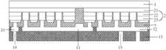
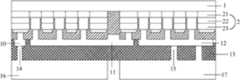
在步骤S1中,提供一衬底1,所述衬底可以是蓝宝石衬底,在所述蓝宝石衬底表面上生长外延层2,所述外延层2的生长过程依次为:在所述衬底表面上生长N型氮化镓层(N-GaN)21,在所述N型氮化镓层21上生长发光层22,在所述发光层22上生长P型氮化镓层(P-GaN)23,对所述外延层2采用感应耦合等离子(ICP)刻蚀方法,去除部分外延层,在所述外延层中形成沟槽3,所述沟槽露出蓝宝石衬底表面,使所述外延层刻蚀成n个彼此相互绝缘独立的芯片,每个芯片可以为正方形,则芯片大小可以是1mm×1mm,每个芯片也可以为长方形,如芯片大小可以是0.5mm×1mm,或芯片还可以是其他大小的芯片,所述n个芯片分别为第一芯片至第n芯片,n为大于等于2的整数,n的取值范围可以是2-100的整数,如图2a和2b所示,图2a所示的是步骤S1后的剖面结构示意图,图2b所示的是步骤S1后的俯视结构示意图。In step S1, a
在步骤S2中,通过光刻和刻蚀技术对每一所述芯片进行刻蚀,以在每一所述芯片表面形成均匀分布的多个小孔4,在本发明的最佳实施例中,每一所述芯片表面形成的小孔的数目为9个,每个所述小孔是直径D为45um的圆孔,所述小孔贯穿P型氮化镓层、发光层,直到停留在N型氮化镓层的表面上,如图3a和3b所示,图3a所示的是步骤S2中形成小孔的剖面结构示意图,图3b所示的是步骤S2中形成小孔的俯视结构示意图。In step S2, each of the chips is etched by photolithography and etching techniques to form a plurality of
然后,在每一所述芯片除所述小孔以外的P型氮化镓层的表面上,采用光刻和腐蚀技术依次沉积NiAg(镍银)金属层,以形成一P型接触层5,优选的,所述镍和银的厚度分别为


在步骤S3中,可以采用溅射、蒸发或喷涂工艺沉积氮化硅(SiN)第一绝缘层7,使所述氮化硅(SiN)第一绝缘层7覆盖在所述外延层和P型接触层的表面以及填充满所述芯片之间的沟槽3和各所述小孔4,优选的,所述氮化硅第一绝缘层的厚度为2um-2.5um,如图5a和5b所示,图5a所示的是步骤S3中形成第一绝缘层的剖面结构示意图,图5b所示的是步骤S3中形成第一绝缘层的俯视结构示意图。In step S3, a first insulating
在步骤S4中,采用光刻和刻蚀技术在所述氮化硅第一绝缘层表面打孔,分别在所述氮化硅第一绝缘层表面刻蚀出N型接触孔8和P型接触孔9,每个所述N型接触孔与一所述N型接触层6的表面连接,优选的,每个所述N型接触孔是直径为30um的圆孔,每个所述P型接触孔与一所述P型接触层5的表面连接,优选的,每个所述P型接触孔是直径为30um的圆孔,在每一所述芯片的P型接触层的表面上均存在P型接触孔,在本实施例中,每一所述芯片的P型接触层的表面上存在3个P型接触孔,具体布置如图6a和图6b所示。图6a所示的是在步骤S4中形成N型接触孔和P型接触孔的剖面结构示意图,图6b所示的是在步骤S4中形成N型接触孔和P型接触孔的俯视结构示意图。In step S4, holes are drilled on the surface of the first insulating layer of silicon nitride by photolithography and etching techniques, and N-type contact holes 8 and P-type contacts are respectively etched on the surface of the first insulating layer of silicon nitride.
在步骤S5中,采用光刻和蒸发技术同步形成第一布线层10、第二布线层11和第三布线层12,所述布线层形成的过程与步骤S2中的N型接触层的形成过程相同,具体参数工艺参见步骤S2,在此不再一一赘述。In step S5, the
其中,在所述第一芯片上的部分第一绝缘层上以及与所述第一芯片的P型接触层连接的P型接触孔内沉积所述第一布线层,也就是说,所述第一布线层通过P型接触孔和第一芯片的P型接触层5连接;Wherein, the first wiring layer is deposited on part of the first insulating layer on the first chip and in the P-type contact hole connected to the P-type contact layer of the first chip, that is to say, the first A wiring layer is connected to the P-
在所述第i芯片和第i+1芯片表面以及两者之间的部分第一绝缘层上以及与所述第i芯片上的N型接触层连接的N型接触孔内,以及与所述第i+1芯片上的P型接触层连接的P型接触孔内沉积所述第二布线层,i为大于等于1且小于n的整数,也就是说,所述第二布线层将所述第一芯片的N型接触层和第二芯片的P型接触层通过第一绝缘层中的N型接触孔和P型接触孔串联,同理,所述第二布线层将所述第二芯片的N型接触层又和第三芯片的P型接触层通过第一绝缘层中的N型接触孔和P型接触孔串联,直至第二布线层将第n-1芯片的N型接触层和第n芯片的P型接触层通过第一绝缘层中的N型接触孔和P型接触孔串联,每两个芯片串联的第二布线层是彼此相互独立的;On the surface of the i-th chip and the i+1-th chip and part of the first insulating layer between them and in the N-type contact hole connected to the N-type contact layer on the i-th chip, and with the The second wiring layer is deposited in the P-type contact hole connected to the P-type contact layer on the i+1 chip, i is an integer greater than or equal to 1 and less than n, that is, the second wiring layer connects the The N-type contact layer of the first chip and the P-type contact layer of the second chip are connected in series through the N-type contact hole and the P-type contact hole in the first insulating layer. Similarly, the second wiring layer connects the second chip The N-type contact layer of the third chip is connected in series with the P-type contact layer of the third chip through the N-type contact hole and the P-type contact hole in the first insulating layer, until the second wiring layer connects the N-type contact layer of the n-1th chip and the P-type contact layer. The P-type contact layer of the nth chip is connected in series through the N-type contact hole and the P-type contact hole in the first insulating layer, and the second wiring layer in which every two chips are connected in series is independent of each other;
在所述第n芯片上的部分第一绝缘层上以及与所述第n芯片上的N型接触层连接的N型接触孔内沉积所述第三布线层,也就是说,所述第三布线层通过N型接触孔和第n芯片的N型接触层连接,如图7a和7b所示,图7a所示的是在步骤S5中形成第一布线层、第二布线层和第三布线层的剖面结构示意图,图7b所示的是在步骤S5中形成第一布线层、第二布线层和第三布线层的俯视结构示意图。The third wiring layer is deposited on part of the first insulating layer on the nth chip and in the N-type contact hole connected to the N-type contact layer on the nth chip, that is to say, the third The wiring layer is connected to the N-type contact layer of the nth chip through the N-type contact hole, as shown in Figures 7a and 7b, and Figure 7a shows that the first wiring layer, the second wiring layer and the third wiring layer are formed in step S5 The schematic diagram of the cross-sectional structure of the layers, FIG. 7b is a schematic diagram of the top view of the first wiring layer, the second wiring layer and the third wiring layer formed in step S5.
在步骤S6中,在所述第一布线层10、第二布线层11和第三布线层12的表面上以及位于所述第一布线层10、第二布线层11和第三布线层12彼此之间的氮化硅第一绝缘层7的表面上,同样可以采用溅射、蒸发或喷涂工艺沉积氮化硅第二绝缘层13,优选的,所述氮化硅第二绝缘层的厚度为2um,如图8a和8b所示,图8a所示的是步骤S6中形成第二绝缘层的剖面结构示意图,图8b所示的是步骤S6中形成第二绝缘层的俯视结构示意图。In step S6, on the surfaces of the
在步骤S7中,采用光刻和刻蚀技术在所述氮化硅第二绝缘层13表面打孔,分别在所述氮化硅第二绝缘层表面刻蚀出第一布线接触孔14和第三布线接触孔15,每个所述第一布线接触孔均与所述第一芯片中的第一布线层的表面连接,优选的,每个所述第一布线接触孔是直径为50um的圆孔,每个所述第三布线接触孔均与所述第n芯片中的第三布线层的表面连接,优选的,每个所述第三布线接触孔是直径为50um的圆孔,本发明中存在至少一个第一布线接触孔和第三布线接触孔,在本实施例中,可以存在3个第一布线接触孔,第三布线接触孔可以为4个,具体布置如图9a和图9b所示,图9a所示的是在步骤S7中形成第一布线接触孔和第三布线接触孔的剖面结构示意图,图9b所示的是在步骤S7中形成第一布线接触孔和第三布线接触孔的俯视结构示意图。In step S7, holes are drilled on the surface of the second silicon
在步骤S8中,采用光刻和蒸发技术制造相互绝缘的一P焊盘16和一N焊盘17,按照本实施例的步骤S2中的过程形成如N型接触层的结构后,再在如N型接触层的结构表面上沉积一锡层形成所述焊盘,优选的,所述锡层的厚度为
实施例二Embodiment two
下面以图1所示的方法流程为例,结合附图2a至10a以及附图2c至10c,对一种倒装高压LED芯片的结构的制造方法进行详细描述。Taking the method flow shown in FIG. 1 as an example, a method for manufacturing a structure of a flip-chip high-voltage LED chip will be described in detail below in conjunction with FIGS. 2a to 10a and FIGS. 2c to 10c.
在步骤S1中,提供一衬底1,所述衬底可以是蓝宝石衬底,在所述蓝宝石衬底表面上生长外延层2,所述外延层2的生长过程依次为:在所述衬底表面上生长N型氮化镓层21,在所述N型氮化镓层21上生长发光层22,在所述发光层22上生长P型氮化镓层23,且使所述P型氮化镓层23的厚度比N型氮化镓层21的厚度薄,对所述外延层2采用ICP刻蚀方法,去除部分外延层,在所述外延层中形成沟槽3,所述沟槽露出蓝宝石衬底表面,使所述外延层刻蚀成n个彼此相互绝缘独立的芯片,每个芯片可以为正方形,则芯片大小可以是1mm×1mm,每个芯片也可以为长方形,如芯片大小可以是0.5mm×1mm,或芯片还可以是其他大小的芯片,所述n个芯片分别为第一芯片至第n芯片,n为大于等于2的整数,n的取值范围可以是2-100的整数,如图2a和2c所示,图2c所示的是步骤S1后的俯视结构示意图。In step S1, a
在步骤S2中,通过光刻和刻蚀技术对每一所述芯片进行刻蚀,以在每一所述芯片表面形成均匀分布的多个小孔4,每一所述芯片表面形成的小孔的数目可以为6个,在本发明的最佳实施例中,每一所述芯片表面形成的小孔的数目为9个,每个所述小孔是直径D为50um的圆孔,所述小孔贯穿P型氮化镓层、发光层,直到停留在N型氮化镓层的表面上,如图3a和3c所示,图3c所示的是步骤S2中形成小孔的俯视结构示意图。In step S2, each of the chips is etched by photolithography and etching techniques to form a plurality of
然后,在每一所述芯片除所述小孔以外的P型氮化镓层的表面上,采用光刻和腐蚀技术沉积一P型接触层5,所述P型接触层如采用氧化铟锡(ITO)透明导电膜形成,优选的,所述P型接触层的厚度为3000?,在每一所述小孔底部的N型氮化镓层表面上沉积一N型接触层6,所述N型接触层形成的过程参见实施例一的步骤S2中的N型接触层,在此不再一一赘述,形成图4a和4c,图4c所示的是步骤S2中形成N型接触层和P型接触层的俯视结构示意图。Then, a P-
在步骤S3中,在所述外延层和P型接触层的表面以及所述芯片之间的沟槽内和各所述小孔内沉积分布布拉格反射镜(DBR)第一绝缘层7,所述DBR第一绝缘层由二氧化硅(SiO2)和二氧化钛(TiO2)的若干周期叠加而形成,优选的,所述DBR第一绝缘层的厚度为2um-2.5um,如图5a和5c所示,图5c所示的是步骤S3中形成第一绝缘层的俯视结构示意图。In step S3, a distributed Bragg reflector (DBR) first insulating
在步骤S4中,采用光刻和刻蚀技术在所述DBR第一绝缘层表面打孔,分别在所述DBR第一绝缘层表面刻蚀出N型接触孔8和P型接触孔9,所述N型接触孔8和P型接触孔9分别形成的过程参见实施例一的步骤S4中的N型接触孔8和P型接触孔9,在此不再一一赘述,与实施例一的步骤S4中的区别在于:每个所述N型接触孔和P型接触孔的大小相同或不同,优选的,每个所述N型接触孔和P型接触孔是直径为35um的圆孔,具体布置如图6a和图6c所示,图6c所示的是在步骤S4中形成N型接触孔和P型接触孔的俯视结构示意图。In step S4, holes are drilled on the surface of the first insulating layer of the DBR using photolithography and etching techniques, and N-type contact holes 8 and P-type contact holes 9 are respectively etched on the surface of the first insulating layer of the DBR. For the process of forming the N-
在步骤S5中,采用光刻和蒸发技术同步形成第一布线层10、第二布线层11和第三布线层12,所述布线层形成的过程参见实施例一的步骤S5,具体参数工艺也请参见实施例一的步骤S5,在此不再一一赘述,形成图7a和7c,图7c所示的是在步骤S5中形成第一布线层、第二布线层和第三布线层的俯视结构示意图。In step S5, the
在步骤S6中,在所述第一布线层10、第二布线层11和第三布线层12的表面上以及位于所述第一布线层10、第二布线层11和第三布线层12彼此之间的DBR第一绝缘层7的表面上沉积氮化硅第二绝缘层13,优选的,所述氮化硅第二绝缘层的厚度为2um-2.5um,如图8a和8c所示,图8c所示的是步骤S6中形成第二绝缘层的俯视结构示意图。In step S6, on the surfaces of the
在步骤S7中,采用光刻和刻蚀技术在所述氮化硅第二绝缘层13表面打孔,分别在所述氮化硅第二绝缘层表面刻蚀出第一布线接触孔14和第三布线接触孔15,每个所述第一布线接触孔均与所述第一芯片中的第一布线层的表面连接,优选的,每个所述第一布线接触孔是直径为50um的圆孔,每个所述第三布线接触孔均与所述第n芯片中的第三布线层的表面连接,优选的,每个所述第三布线接触孔是直径为50um的圆孔,本发明中存在至少一个第一布线接触孔和第三布线接触孔,在本发明的最佳实施例中,存在3个第一布线接触孔,第三布线接触孔4个,具体布置如图9a和图9c所示,图9c所示的是在步骤S7中形成第一布线接触孔和第三布线接触孔的俯视结构示意图。In step S7, holes are drilled on the surface of the second silicon
在步骤S8中,采用光刻和蒸发技术制造相互绝缘的一P焊盘16和一N焊盘17,按照实施例一的步骤S2中的过程形成如N型接触层的结构后,再在如N型接触层的表面上沉积一锡层形成所述焊盘,优选的,所述锡层的厚度为
在实施例一和实施例二中,所述第一绝缘层和第二绝缘层使用的材料还可为氮化铝,二氧化硅,氮氧化硅,三氧化二铝或聚酰亚胺中的一种。In
通过实施例一和实施例二,本发明还可以提供一种倒装高压LED芯片,包括:Through
衬底,位于所述衬底表面上彼此互相绝缘独立的第一至第n芯片,n为大于等于2的整数,每一所述芯片包括位于衬底表面上的N型氮化镓层、位于所述N型氮化镓层上的发光层、以及位于所述发光层上的P型氮化镓层;每一所述芯片表面均匀分布的贯穿P型氮化镓层、发光层直到停留在N型氮化镓层表面上的小孔,位于每一所述小孔内的N型氮化镓层表面上的一N型接触层,位于每一所述芯片的P型氮化镓层表面上的一P型接触层;位于所述芯片之间及所述N型接触层和P型接触层之间的第一绝缘层;分别贯穿所述第一绝缘层、直到与所述N型接触层互连的N型接触孔和直到与所述P型接触层互连的P型接触孔;第一布线层,位于所述第一芯片上的部分第一绝缘层上且填充满与所述第一芯片上的P型接触层连接的P型接触孔;第二布线层,位于所述第i芯片和第i+1芯片之间的部分第一绝缘层上且填充满与所述第i芯片上的N型接触层连接的N型接触孔,以及填充满与所述第i+1芯片上的P型接触层连接的P型接触孔,i为大于等于1且小于n的整数;第三布线层,位于所述第n芯片上的部分绝缘层上且填充满与所述第n芯片上的N型接触层连接的N型接触孔;第二绝缘层,位于所述第一布线层、第二布线层和第三布线层的表面上及位于所述第一布线层、第二布线层和第三布线层彼此之间的第一绝缘层表面上;分别贯穿所述第二绝缘层、直到与所述第一布线层互连的第一布线接触孔和直到与所述第三布线层互连的第三布线接触孔;以及相互绝缘的P焊盘和N焊盘,所述P焊盘位于所述第二绝缘层的一半表面上且填充满所述第一布线接触孔,所述N焊盘位于所述绝缘层的另一半表面上且填充满所述第三布线接触孔。The substrate, the first to nth chips that are mutually insulated and independent from each other on the surface of the substrate, n is an integer greater than or equal to 2, each of the chips includes an N-type gallium nitride layer on the surface of the substrate, located on The light-emitting layer on the N-type gallium nitride layer, and the P-type gallium nitride layer on the light-emitting layer; the surface of each chip is evenly distributed through the P-type gallium nitride layer and the light-emitting layer until it stays on the Small holes on the surface of the N-type gallium nitride layer, an N-type contact layer on the surface of the N-type gallium nitride layer in each of the small holes, and an N-type contact layer on the surface of the P-type gallium nitride layer on each of the chips A P-type contact layer on the top; a first insulating layer located between the chips and between the N-type contact layer and the P-type contact layer; respectively penetrating through the first insulating layer until it contacts the N-type The N-type contact hole for layer interconnection and the P-type contact hole until it is interconnected with the P-type contact layer; the first wiring layer is located on a part of the first insulating layer on the first chip and is filled with the The P-type contact hole connected to the P-type contact layer on the first chip; the second wiring layer is located on a part of the first insulating layer between the i-th chip and the i+1-th chip and is filled with the i-th chip. The N-type contact hole connected to the N-type contact layer on the chip, and the P-type contact hole connected to the P-type contact layer on the i+1th chip, i is an integer greater than or equal to 1 and less than n; The third wiring layer is located on a part of the insulating layer on the nth chip and fills the N-type contact hole connected to the N-type contact layer on the nth chip; the second insulating layer is located on the first wiring layer , on the surface of the second wiring layer and the third wiring layer and on the surface of the first insulating layer between the first wiring layer, the second wiring layer and the third wiring layer; through the second insulating layer respectively , until the first wiring contact hole interconnected with the first wiring layer and until the third wiring contact hole interconnected with the third wiring layer; and a P pad and an N pad that are insulated from each other, the P The pad is located on a half surface of the second insulating layer and fills the first wiring contact hole, and the N pad is located on the other half surface of the insulating layer and fills the third wiring contact hole.
由实施例一和实施例二的制造方法获得的倒装高压LED芯片,不仅可以做成大芯片,由于两个焊盘对称分布、倒装接触面积大,且P型氮化镓层比N型氮化镓层薄,使发光层离基板近,可以很容易的将热量导出,因此本发明公开的倒装高压LED芯片的散热速度快,散热效果非常好,电流密度小,发热少;此外,本发明公开的倒装高压LED芯片兼有高压芯片高电压低电流的优势,电路简单;另外,本发明的倒装高压LED芯片一方面不用客户打线,另一方面倒装焊接对准容易,对电路板布置要求精度低,倒装焊接工艺简单,同时兼有倒装芯片避开了电极和引线挡光的问题,同样提高芯片的光效,且封装工艺简单。The flip-chip high-voltage LED chip obtained by the manufacturing methods of
本发明虽然以较佳实施例公开如上,但其并不是用来限定权利要求,任何本领域技术人员在不脱离本发明的精神和范围内,都可以做出可能的变动和修改,因此本发明的保护范围应当以本发明权利要求所界定的范围为准。Although the present invention is disclosed as above with preferred embodiments, it is not used to limit the claims. Any person skilled in the art can make possible changes and modifications without departing from the spirit and scope of the present invention. Therefore, the present invention The scope of protection should be based on the scope defined by the claims of the present invention.
Claims (7)
Priority Applications (1)
| Application Number | Priority Date | Filing Date | Title |
|---|---|---|---|
| CN201310465534.7ACN103500790B (en) | 2013-10-08 | 2013-10-08 | A kind of structure and manufacture method thereof of upside-down mounting high-voltage LED chip |
Applications Claiming Priority (1)
| Application Number | Priority Date | Filing Date | Title |
|---|---|---|---|
| CN201310465534.7ACN103500790B (en) | 2013-10-08 | 2013-10-08 | A kind of structure and manufacture method thereof of upside-down mounting high-voltage LED chip |
Publications (2)
| Publication Number | Publication Date |
|---|---|
| CN103500790Atrue CN103500790A (en) | 2014-01-08 |
| CN103500790B CN103500790B (en) | 2016-05-25 |
Family
ID=49865977
Family Applications (1)
| Application Number | Title | Priority Date | Filing Date |
|---|---|---|---|
| CN201310465534.7AActiveCN103500790B (en) | 2013-10-08 | 2013-10-08 | A kind of structure and manufacture method thereof of upside-down mounting high-voltage LED chip |
Country Status (1)
| Country | Link |
|---|---|
| CN (1) | CN103500790B (en) |
Cited By (21)
| Publication number | Priority date | Publication date | Assignee | Title |
|---|---|---|---|---|
| CN103956419A (en)* | 2014-04-28 | 2014-07-30 | 深圳大学 | LED chip and manufacturing method thereof |
| CN104103733A (en)* | 2014-06-18 | 2014-10-15 | 华灿光电(苏州)有限公司 | Inverted light emitting diode chip and fabrication method thereof |
| CN104134744A (en)* | 2014-08-08 | 2014-11-05 | 映瑞光电科技(上海)有限公司 | High-voltage flip LED chip easy to package and manufacturing method thereof |
| CN104269486A (en)* | 2014-09-15 | 2015-01-07 | 映瑞光电科技(上海)有限公司 | Flip LED chip and manufacturing method thereof |
| CN104409617A (en)* | 2014-11-28 | 2015-03-11 | 杭州士兰明芯科技有限公司 | Flip LED chip and manufacturing method thereof |
| CN104465974A (en)* | 2014-12-03 | 2015-03-25 | 佛山市国星半导体技术有限公司 | Light-emitting diode and manufacturing method thereof |
| CN104485343A (en)* | 2014-12-29 | 2015-04-01 | 杭州士兰微电子股份有限公司 | LED flip chip and manufacturing method thereof |
| CN104779339A (en)* | 2015-01-15 | 2015-07-15 | 大连德豪光电科技有限公司 | Inverted high-voltage LED chip and preparation method thereof |
| CN104993031A (en)* | 2015-06-12 | 2015-10-21 | 映瑞光电科技(上海)有限公司 | High-voltage inversion LED chip and manufacturing method thereof |
| CN105322066A (en)* | 2014-07-10 | 2016-02-10 | 晶元光电股份有限公司 | Photoelectric element and its manufacturing method |
| CN105449084A (en)* | 2015-12-22 | 2016-03-30 | 浙江师范大学 | Inversed high-voltage light emitting diode (LED) chip electrode and chip fabrication method |
| CN106159043A (en)* | 2015-04-01 | 2016-11-23 | 映瑞光电科技(上海)有限公司 | Flip LED chips and forming method thereof |
| CN106159056A (en)* | 2016-09-18 | 2016-11-23 | 佛山市国星半导体技术有限公司 | A kind of upside-down mounting high-voltage chip and preparation method thereof |
| CN106299095A (en)* | 2015-06-12 | 2017-01-04 | 映瑞光电科技(上海)有限公司 | A kind of high pressure flip LED chips and preparation method thereof |
| JP2017112166A (en)* | 2015-12-15 | 2017-06-22 | スタンレー電気株式会社 | Semiconductor light emitting element array and vehicle lamp |
| CN106935607A (en)* | 2015-12-31 | 2017-07-07 | 晶能光电(江西)有限公司 | A kind of upside-down mounting high voltage LED chip and preparation method thereof |
| CN107068825A (en)* | 2017-02-14 | 2017-08-18 | 盐城东紫光电科技有限公司 | A kind of high pressure flip LED chips structure and its manufacture method |
| CN108493306A (en)* | 2018-03-27 | 2018-09-04 | 北京大学 | A kind of preparation method of high voltage and high power GaN base LED array chip |
| US10529893B2 (en) | 2014-07-03 | 2020-01-07 | Epistar Corporation | Optoelectronic device and method for manufacturing the same |
| CN114256389A (en)* | 2021-12-13 | 2022-03-29 | 广东省科学院半导体研究所 | High-density micro LED array and manufacturing method and application thereof |
| CN114899287A (en)* | 2022-04-20 | 2022-08-12 | 厦门士兰明镓化合物半导体有限公司 | Light-emitting diode and method of making the same |
Families Citing this family (1)
| Publication number | Priority date | Publication date | Assignee | Title |
|---|---|---|---|---|
| TWI692115B (en)* | 2016-06-28 | 2020-04-21 | 晶元光電股份有限公司 | Light emitting element |
Citations (4)
| Publication number | Priority date | Publication date | Assignee | Title |
|---|---|---|---|---|
| US20050133797A1 (en)* | 2003-12-23 | 2005-06-23 | Samsung Electronics Co., Ltd. | Flip-chip light emitting diode and method of manufacturing the same |
| US20060261358A1 (en)* | 2005-05-03 | 2006-11-23 | Samsung Electro-Mechanics Co., Ltd. | Flip chip light emitting diode and method of manufacturing the same |
| CN102339913A (en)* | 2011-09-30 | 2012-02-01 | 映瑞光电科技(上海)有限公司 | High-voltage LED (Light Emitting Diode) device and manufacturing method thereof |
| CN203536473U (en)* | 2013-10-08 | 2014-04-09 | 杭州士兰明芯科技有限公司 | Flip chip structure of high-voltage LED chips |
- 2013
- 2013-10-08CNCN201310465534.7Apatent/CN103500790B/enactiveActive
Patent Citations (4)
| Publication number | Priority date | Publication date | Assignee | Title |
|---|---|---|---|---|
| US20050133797A1 (en)* | 2003-12-23 | 2005-06-23 | Samsung Electronics Co., Ltd. | Flip-chip light emitting diode and method of manufacturing the same |
| US20060261358A1 (en)* | 2005-05-03 | 2006-11-23 | Samsung Electro-Mechanics Co., Ltd. | Flip chip light emitting diode and method of manufacturing the same |
| CN102339913A (en)* | 2011-09-30 | 2012-02-01 | 映瑞光电科技(上海)有限公司 | High-voltage LED (Light Emitting Diode) device and manufacturing method thereof |
| CN203536473U (en)* | 2013-10-08 | 2014-04-09 | 杭州士兰明芯科技有限公司 | Flip chip structure of high-voltage LED chips |
Cited By (36)
| Publication number | Priority date | Publication date | Assignee | Title |
|---|---|---|---|---|
| CN103956419A (en)* | 2014-04-28 | 2014-07-30 | 深圳大学 | LED chip and manufacturing method thereof |
| CN103956419B (en)* | 2014-04-28 | 2018-01-16 | 深圳大学 | A kind of LED chip and preparation method thereof |
| CN104103733A (en)* | 2014-06-18 | 2014-10-15 | 华灿光电(苏州)有限公司 | Inverted light emitting diode chip and fabrication method thereof |
| US11908975B2 (en) | 2014-07-03 | 2024-02-20 | Epistar Corporation | Optoelectronic device and method for manufacturing the same |
| US11011679B2 (en) | 2014-07-03 | 2021-05-18 | Epistar Corporation | Optoelectronic device and method for manufacturing the same |
| US12218279B2 (en) | 2014-07-03 | 2025-02-04 | Epistar Corporation | Optoelectronic device and method for manufacturing the same |
| US10529893B2 (en) | 2014-07-03 | 2020-01-07 | Epistar Corporation | Optoelectronic device and method for manufacturing the same |
| CN105322066A (en)* | 2014-07-10 | 2016-02-10 | 晶元光电股份有限公司 | Photoelectric element and its manufacturing method |
| CN105322066B (en)* | 2014-07-10 | 2020-11-27 | 晶元光电股份有限公司 | Photoelectric element and method of manufacturing the same |
| CN104134744A (en)* | 2014-08-08 | 2014-11-05 | 映瑞光电科技(上海)有限公司 | High-voltage flip LED chip easy to package and manufacturing method thereof |
| CN104269486A (en)* | 2014-09-15 | 2015-01-07 | 映瑞光电科技(上海)有限公司 | Flip LED chip and manufacturing method thereof |
| CN104409617A (en)* | 2014-11-28 | 2015-03-11 | 杭州士兰明芯科技有限公司 | Flip LED chip and manufacturing method thereof |
| CN104409617B (en)* | 2014-11-28 | 2017-02-22 | 杭州士兰明芯科技有限公司 | Flip LED chip and manufacturing method thereof |
| CN104465974B (en)* | 2014-12-03 | 2017-08-04 | 佛山市国星半导体技术有限公司 | A light emitting diode and its manufacturing method |
| CN104465974A (en)* | 2014-12-03 | 2015-03-25 | 佛山市国星半导体技术有限公司 | Light-emitting diode and manufacturing method thereof |
| CN104485343B (en)* | 2014-12-29 | 2018-01-23 | 杭州士兰微电子股份有限公司 | Flip LED chips and preparation method thereof |
| CN104485343A (en)* | 2014-12-29 | 2015-04-01 | 杭州士兰微电子股份有限公司 | LED flip chip and manufacturing method thereof |
| CN104779339B (en)* | 2015-01-15 | 2017-08-25 | 大连德豪光电科技有限公司 | Upside-down mounting high voltage LED chip and preparation method thereof |
| CN104779339A (en)* | 2015-01-15 | 2015-07-15 | 大连德豪光电科技有限公司 | Inverted high-voltage LED chip and preparation method thereof |
| CN106159043B (en)* | 2015-04-01 | 2019-12-13 | 映瑞光电科技(上海)有限公司 | Flip LED chip and forming method thereof |
| CN106159043A (en)* | 2015-04-01 | 2016-11-23 | 映瑞光电科技(上海)有限公司 | Flip LED chips and forming method thereof |
| CN104993031B (en)* | 2015-06-12 | 2018-03-06 | 映瑞光电科技(上海)有限公司 | High pressure flip LED chips and its manufacture method |
| CN104993031A (en)* | 2015-06-12 | 2015-10-21 | 映瑞光电科技(上海)有限公司 | High-voltage inversion LED chip and manufacturing method thereof |
| CN106299095A (en)* | 2015-06-12 | 2017-01-04 | 映瑞光电科技(上海)有限公司 | A kind of high pressure flip LED chips and preparation method thereof |
| JP2017112166A (en)* | 2015-12-15 | 2017-06-22 | スタンレー電気株式会社 | Semiconductor light emitting element array and vehicle lamp |
| CN105449084B (en)* | 2015-12-22 | 2018-06-29 | 浙江师范大学 | A kind of upside-down mounting high voltage LED chip electrode and manufacturing method of chip |
| CN105449084A (en)* | 2015-12-22 | 2016-03-30 | 浙江师范大学 | Inversed high-voltage light emitting diode (LED) chip electrode and chip fabrication method |
| CN106935607A (en)* | 2015-12-31 | 2017-07-07 | 晶能光电(江西)有限公司 | A kind of upside-down mounting high voltage LED chip and preparation method thereof |
| CN106159056A (en)* | 2016-09-18 | 2016-11-23 | 佛山市国星半导体技术有限公司 | A kind of upside-down mounting high-voltage chip and preparation method thereof |
| CN107068825A (en)* | 2017-02-14 | 2017-08-18 | 盐城东紫光电科技有限公司 | A kind of high pressure flip LED chips structure and its manufacture method |
| CN108493306B (en)* | 2018-03-27 | 2020-09-08 | 北京大学 | A kind of preparation method of high voltage and high power GaN-based LED array chip |
| CN108493306A (en)* | 2018-03-27 | 2018-09-04 | 北京大学 | A kind of preparation method of high voltage and high power GaN base LED array chip |
| CN114256389A (en)* | 2021-12-13 | 2022-03-29 | 广东省科学院半导体研究所 | High-density micro LED array and manufacturing method and application thereof |
| CN114256389B (en)* | 2021-12-13 | 2024-05-17 | 广东省科学院半导体研究所 | A high-density micro LED array and its manufacturing method and application |
| CN114899287A (en)* | 2022-04-20 | 2022-08-12 | 厦门士兰明镓化合物半导体有限公司 | Light-emitting diode and method of making the same |
| CN114899287B (en)* | 2022-04-20 | 2025-08-12 | 厦门士兰明镓化合物半导体有限公司 | Light emitting diode and method of manufacturing the same |
Also Published As
| Publication number | Publication date |
|---|---|
| CN103500790B (en) | 2016-05-25 |
Similar Documents
| Publication | Publication Date | Title |
|---|---|---|
| CN103500790B (en) | A kind of structure and manufacture method thereof of upside-down mounting high-voltage LED chip | |
| CN101515621B (en) | Light emitting diode chip, manufacturing method and packaging method | |
| CN105552180B (en) | A kind of production method of novel high-pressure LED | |
| CN102270633B (en) | High-power flip-chip array LED chip and manufacturing method thereof | |
| CN104300056B (en) | A kind of preparation method of the flip LED chips of high reliability, LED component and LED chip | |
| CN101868866A (en) | Improved Light Emitting Diode Structure | |
| CN105789408A (en) | Method for manufacturing light-emitting diode packaging structure and light-emitting diode element | |
| CN104779339B (en) | Upside-down mounting high voltage LED chip and preparation method thereof | |
| CN104064634A (en) | A method for manufacturing a high-brightness GaN-based eutectic welding light-emitting diode | |
| CN105489721B (en) | A kind of LED flip chip containing reflecting layer and preparation method thereof | |
| CN110085620B (en) | Micro-array integrated LED chip and preparation method thereof | |
| CN103378244A (en) | Light emitting diode device and manufacturing method thereof | |
| CN105489742B (en) | A kind of LED flip chip and preparation method thereof | |
| CN102332521A (en) | Gallium nitride-based light-emitting diode with point-like distributed N electrodes and preparation method thereof | |
| CN106981550A (en) | A kind of easily encapsulation easy heat radiation upside-down mounting high voltage LED chip | |
| CN109326688B (en) | A double-metal layer annular interdigital electrode flip-chip LED chip and its manufacturing method | |
| CN105591002A (en) | LED flip chip with reflection layer and preparation method thereof | |
| CN106848006A (en) | Flip LED chips and preparation method thereof | |
| CN102386178B (en) | A kind of LED of high drive and manufacture method thereof | |
| JP2021527965A (en) | Semiconductor light emitting device | |
| CN105633238A (en) | Inverted LED (light emitting diode) chip and manufacturing method thereof | |
| CN109638125B (en) | A flip-chip LED chip and method of making the same | |
| CN203536473U (en) | Flip chip structure of high-voltage LED chips | |
| CN106848005B (en) | Flip-chip LED chip with improved brightness and preparation method thereof | |
| CN102522400A (en) | Anti-electrostatic-damage vertical light-emitting device and manufacturing method thereof |
Legal Events
| Date | Code | Title | Description |
|---|---|---|---|
| C06 | Publication | ||
| PB01 | Publication | ||
| C10 | Entry into substantive examination | ||
| SE01 | Entry into force of request for substantive examination | ||
| C14 | Grant of patent or utility model | ||
| GR01 | Patent grant | ||
| TR01 | Transfer of patent right | ||
| TR01 | Transfer of patent right | Effective date of registration:20241224 Address after:310018 No. 308, No. 10 Street (East) of Hangzhou Economic and Technological Development Zone, Zhejiang Province Patentee after:HANGZHOU SILAN INTEGRATED CIRCUIT Co.,Ltd. Country or region after:China Address before:No. 300, 10th Street, Baiyang Street, Hangzhou Economic and Technological Development Zone, Hangzhou City, Zhejiang Province 310018 Patentee before:HANGZHOU SILAN AZURE Co.,Ltd. Country or region before:China |