CN103500774A - Method for utilizing P-type silicon ball as boron source to prepare local back field - Google Patents
Method for utilizing P-type silicon ball as boron source to prepare local back fieldDownload PDFInfo
- Publication number
- CN103500774A CN103500774ACN201310426654.6ACN201310426654ACN103500774ACN 103500774 ACN103500774 ACN 103500774ACN 201310426654 ACN201310426654 ACN 201310426654ACN 103500774 ACN103500774 ACN 103500774A
- Authority
- CN
- China
- Prior art keywords
- silicon
- printing
- type silicon
- boron
- back field
- Prior art date
- Legal status (The legal status is an assumption and is not a legal conclusion. Google has not performed a legal analysis and makes no representation as to the accuracy of the status listed.)
- Granted
Links
Images
Classifications
- H—ELECTRICITY
- H10—SEMICONDUCTOR DEVICES; ELECTRIC SOLID-STATE DEVICES NOT OTHERWISE PROVIDED FOR
- H10F—INORGANIC SEMICONDUCTOR DEVICES SENSITIVE TO INFRARED RADIATION, LIGHT, ELECTROMAGNETIC RADIATION OF SHORTER WAVELENGTH OR CORPUSCULAR RADIATION
- H10F77/00—Constructional details of devices covered by this subclass
- H10F77/20—Electrodes
- H10F77/206—Electrodes for devices having potential barriers
- H10F77/211—Electrodes for devices having potential barriers for photovoltaic cells
- H10F77/219—Arrangements for electrodes of back-contact photovoltaic cells
- H—ELECTRICITY
- H10—SEMICONDUCTOR DEVICES; ELECTRIC SOLID-STATE DEVICES NOT OTHERWISE PROVIDED FOR
- H10F—INORGANIC SEMICONDUCTOR DEVICES SENSITIVE TO INFRARED RADIATION, LIGHT, ELECTROMAGNETIC RADIATION OF SHORTER WAVELENGTH OR CORPUSCULAR RADIATION
- H10F71/00—Manufacture or treatment of devices covered by this subclass
- Y—GENERAL TAGGING OF NEW TECHNOLOGICAL DEVELOPMENTS; GENERAL TAGGING OF CROSS-SECTIONAL TECHNOLOGIES SPANNING OVER SEVERAL SECTIONS OF THE IPC; TECHNICAL SUBJECTS COVERED BY FORMER USPC CROSS-REFERENCE ART COLLECTIONS [XRACs] AND DIGESTS
- Y02—TECHNOLOGIES OR APPLICATIONS FOR MITIGATION OR ADAPTATION AGAINST CLIMATE CHANGE
- Y02E—REDUCTION OF GREENHOUSE GAS [GHG] EMISSIONS, RELATED TO ENERGY GENERATION, TRANSMISSION OR DISTRIBUTION
- Y02E10/00—Energy generation through renewable energy sources
- Y02E10/50—Photovoltaic [PV] energy
- Y—GENERAL TAGGING OF NEW TECHNOLOGICAL DEVELOPMENTS; GENERAL TAGGING OF CROSS-SECTIONAL TECHNOLOGIES SPANNING OVER SEVERAL SECTIONS OF THE IPC; TECHNICAL SUBJECTS COVERED BY FORMER USPC CROSS-REFERENCE ART COLLECTIONS [XRACs] AND DIGESTS
- Y02—TECHNOLOGIES OR APPLICATIONS FOR MITIGATION OR ADAPTATION AGAINST CLIMATE CHANGE
- Y02P—CLIMATE CHANGE MITIGATION TECHNOLOGIES IN THE PRODUCTION OR PROCESSING OF GOODS
- Y02P70/00—Climate change mitigation technologies in the production process for final industrial or consumer products
- Y02P70/50—Manufacturing or production processes characterised by the final manufactured product
Landscapes
- Photovoltaic Devices (AREA)
Abstract
Translated fromChinese
Description
Translated fromChinesethe
技术领域technical field
本发明涉及一种太阳能电池制备工艺,具体涉及一种利用P型硅球作为硼源制备局部背场的工艺方法。The invention relates to a solar cell preparation process, in particular to a process method for preparing a local back field by using a P-type silicon sphere as a boron source.
the
背景技术Background technique
在当今的太阳能研究中热点问题中,背场对电池表面的钝化和吸杂作用的研究一直受到太阳能光伏科研人员的关注。研究主要集中在以下三个方面:(1)铝背场制备工艺方法以及热处理方法;(2)制备背场的材料;(3)在太阳电池中,铝背场的吸杂作用和钝化作用。本发明涉及一种制备背场的新材料。Among the hot issues in today's solar energy research, the research on the passivation and gettering effect of the back field on the battery surface has always been concerned by solar photovoltaic researchers. The research mainly focuses on the following three aspects: (1) the preparation process and heat treatment method of the aluminum back field; (2) the preparation of the back field material; (3) the gettering effect and passivation of the aluminum back field in the solar cell . The invention relates to a new material for preparing a back field.
全铝背场虽然已经大大降低了电池背表面载流子复合速率,但是由于电池基片越来越薄,铝背场的不均匀等问题,导致其已经不能满足制备高效太阳电池的要求。所以研究者开始研究制备局部铝背场,特别是运用硼背场和背面纯化层的方法,发现电池背表面的载流子复合速度得到了进一步降低。Although the all-aluminum back field has greatly reduced the carrier recombination rate on the back surface of the battery, it can no longer meet the requirements of preparing high-efficiency solar cells due to the thinner and thinner battery substrates and the unevenness of the aluminum back field. Therefore, researchers began to study the preparation of local aluminum back field, especially the method of using boron back field and back purification layer, and found that the carrier recombination speed on the back surface of the battery was further reduced.
为弥补全铝背场的不足,制备更高效的太阳能电池,局域背场工艺的出现成为必然, 由于硼在晶体硅中的最大饱和固溶度远大于铝, 跟常规局部铝背场相比,研究者发现硼背场对于提高太阳能电池少数载流子寿命以及硅基太阳能电池表面纯化作用方面效果更好。很多学者对局域硼背场的制备做了大量研究,例如赵建华博士(24.5% Effciency Silicon PERT Cells on MCZ Substrates and 24.7% Effciency PERL Cells on FZ Substrates,Prog. Photovolt: Res. Appl.1999)提出的PREL结构利用BBr3作为硼源进行背场局部掺杂,实现了24.7%的电池转化效率,是迄今为止报道的硅基太阳能电池最高的电池转化效率;德国的Sven Kluska(High-Efficiency Silicon Solar Cells With Boron Local Back Surface Fields Formed by Laser Chemical Processing,IEEE,2011)提出采用激光化学加工的方法实现局部硼背场的掺杂,实现电池效率20.9%;无锡尚德的Zhenjiao Wang, Peiyu Han(Advanced PERC and PERL production cells with 20.3%record efficiency for standard commercial p-type silicon wafers,Prog. Photovolt: Res. Appl. 2012)等提出采用局部硼扩散的方法能制备效率超过20%的Pluto cell电池也已经得到证实。In order to make up for the deficiency of the all-aluminum back field and prepare more efficient solar cells, the emergence of localized back field technology has become inevitable. Since the maximum saturated solid solubility of boron in crystalline silicon is much greater than that of aluminum, compared with the conventional localized aluminum back field , the researchers found that the boron back field is more effective in improving the minority carrier lifetime of solar cells and the surface purification of silicon-based solar cells. Many scholars have done a lot of research on the preparation of local boron back field, such as Dr. Zhao Jianhua (24.5% Effciency Silicon PERT Cells on MCZ Substrates and 24.7% Effciency PERL Cells on FZ Substrates, Prog. Photovolt: Res. Appl.1999) proposed The PREL structure uses BBr3 as a boron source for local doping of the back field, achieving a cell conversion efficiency of 24.7%, which is the highest cell conversion efficiency reported so far for silicon-based solar cells; Germany's Sven Kluska (High-Efficiency Silicon Solar Cells With Boron Local Back Surface Fields Formed by Laser Chemical Processing, IEEE, 2011) proposed to use laser chemical processing to achieve local boron back field doping, achieving a cell efficiency of 20.9%; Wuxi Suntech's Zhenjiao Wang, Peiyu Han (Advanced PERC and PERL production cells with 20.3% record efficiency for standard commercial p-type silicon wafers, Prog. Photovolt: Res. Appl. 2012) and others have proposed that Pluto cell batteries with an efficiency of more than 20% can be prepared by using local boron diffusion.
综上所述,目前报道的背场硼掺杂工艺主要采用:1)利用激光化学的方法;2)采用液态或气态硼源高温扩散;3)沉积掺硼氧化硅薄膜等方法。但是,由于以上工艺中硼的扩散均要在1000℃以上的高温下完成,激光化学方法的局部温度也极高,导致晶体内部结构发生变化,产生二次缺陷,对硅片质量影响较大,从而降低太阳能电池的性能;再次以上方法均面临着设备昂贵,工艺的生产成本过高,不能与现行的工艺兼容等问题,均导致背场硼掺杂工艺一直不适用于现代工业化生产。To sum up, the back-field boron doping process currently reported mainly adopts: 1) the method of using laser chemistry; 2) the high-temperature diffusion of liquid or gaseous boron source; 3) the deposition of boron-doped silicon oxide film and other methods. However, since the diffusion of boron in the above processes must be completed at a high temperature above 1000°C, the local temperature of the laser chemical method is also extremely high, resulting in changes in the internal structure of the crystal and secondary defects, which have a great impact on the quality of the silicon wafer. Thereby reducing the performance of the solar cell; again, the above methods all face problems such as expensive equipment, high production cost of the process, and incompatibility with the current process, which all lead to the back-field boron doping process that has not been suitable for modern industrial production.
the
发明内容Contents of the invention
本发明提供一种低成本,与现行工艺兼容的,可工业化生产,高生产率的采用P型硅球作为硼源制造局部背场的方法,克服现有技术中成本高、需要特殊的生产设备以及硼扩散带来的高温热损伤、进而解决约束太阳能电池性能提升的问题。主要是通过将P型硅球配制为印浆之后,印刷于背场而制得。具体的技术方案是:The present invention provides a low-cost, compatible with the current process, industrialized production, high productivity method using P-type silicon balls as boron source to manufacture local back field, which overcomes the high cost in the prior art, the need for special production equipment and The high-temperature thermal damage caused by boron diffusion can solve the problem that restricts the performance improvement of solar cells. It is mainly made by preparing P-type silicon balls as printing paste and printing them on the back field. The specific technical solutions are:
一种利用P型硅球作为硼源制备局部背场的方法,包括如下步骤:A method utilizing P-type silicon spheres as a boron source to prepare a local back field, comprising the steps of:
第1步、将硅片进行制绒、清洗、扩散、边缘刻蚀及去磷硅玻璃,得到前工艺硅片;Step 1: Carry out texturing, cleaning, diffusion, edge etching and dephosphorous silicon glass on the silicon wafer to obtain the silicon wafer of the previous process;
第2步、将P型硅球混合于印浆中,再印刷于第1步所得的前工艺硅片背面,烘干后再进行退火,得到带硼掺杂局部背场的硅片;Step 2: Mix P-type silicon balls in the printing paste, and then print on the back of the pre-process silicon wafer obtained in the first step, dry and then anneal to obtain a silicon wafer with boron-doped local back field;
第3步、在第2步所得的硼掺杂局部背场的硅片的背面沉积钝化膜;Step 3, depositing a passivation film on the back side of the boron-doped local back field silicon wafer obtained in step 2;
第4步、背面将银浆套印于烘干后的印浆表面,再进行烘干;Step 4, overprint the silver paste on the surface of the dried printing paste on the back, and then dry it;
第5步、对硅片进行烧结,使银浆和硅硼掺杂区域形成欧姆接触。Step 5, sintering the silicon wafer to form ohmic contact between the silver paste and the silicon-boron doped region.
本发明的技术方案中,第1步中所使用的硅片可以是太阳能电池使用的单晶硅片,也可以采用多晶硅片,采用常规的前处理工艺即可。In the technical solution of the present invention, the silicon wafer used in the first step may be a monocrystalline silicon wafer used in solar cells, or a polycrystalline silicon wafer, and a conventional pretreatment process may be used.
第2步的目的是使P型硅球作为硼源粘附于硅片背面,采用的是将P型硅球配于印浆中,再印刷于硅片的背面,可以采用常规的印刷方式将含有硅球的印浆印于背面上,比较优选的方式是通过丝网印刷或者喷墨打印的方法,该两种方法印刷的图案可调,技术较为成熟,印刷过程易于控制,而且通过丝网印刷或者喷墨打印时,形成的图案的厚度、尺寸都可以控制得较小,在退火、烧结的工序中,以较低的温度和较短的时间进行处理即可,这样可以降低硅片的热损伤,提高电池性能。印浆在背面的图案可以根据实际情况优化:若为点状时,点直径范围可以为70~250μm,点间距的范围可以为100~2000μm(本发明所称的点间距是指两点的中心之间的距离);若为线状阵列时,线宽范围可以是70~200μm,线间距可以是100~2000μm(本发明所称的线间距是指线宽的中心之间的距离)。采用印刷的方式可以简单、方便地控制硅球印浆的图案,而且采用的是常见设备,简便易行。另外,采用印刷的方式可以一次性地整体在硅片的背面上形成印刷图案,再进行整体烘干和退火等后序步骤,有利于节约加工时间。经退火后印浆和硅基片间形成良好的附着力。通过合理的控制退火温度和时间,避免硅基片由于1000℃以上高温或者激光热解的瞬时高温而产生热损伤,既降低了生产成本又获得了良好的硅片性能。在整个背场制备完毕后,背场串联电阻明显降低,导电性能增强,电流密度增加。The purpose of the second step is to make the P-type silicon balls adhere to the back of the silicon wafer as a boron source. The method is to mix the P-type silicon balls in the printing paste and then print them on the back of the silicon wafer. The ink paste containing silicon balls is printed on the back. The preferred method is screen printing or inkjet printing. The patterns printed by these two methods are adjustable, the technology is relatively mature, and the printing process is easy to control. When printing or inkjet printing, the thickness and size of the formed pattern can be controlled to be small. In the process of annealing and sintering, it can be processed at a lower temperature and a shorter time, which can reduce the silicon wafer. thermal damage and improve battery performance. The pattern on the back of the printing paste can be optimized according to the actual situation: if it is dot-shaped, the dot diameter range can be 70-250 μm, and the dot pitch range can be 100-2000 μm (the dot spacing referred to in the present invention refers to the center of two points. If it is a linear array, the line width range can be 70-200 μm, and the line spacing can be 100-2000 μm (the line spacing referred to in the present invention refers to the distance between the centers of the line width). The pattern of silicon ball printing paste can be controlled simply and conveniently by printing, and common equipment is used, which is simple and easy to operate. In addition, the printing method can be used to form a printed pattern on the back of the silicon wafer at one time, and then perform subsequent steps such as overall drying and annealing, which is beneficial to save processing time. After annealing, good adhesion is formed between the printing paste and the silicon substrate. By reasonably controlling the annealing temperature and time, thermal damage to the silicon substrate due to high temperature above 1000°C or instantaneous high temperature caused by laser pyrolysis is avoided, which not only reduces the production cost but also obtains good performance of the silicon wafer. After the entire back field is prepared, the series resistance of the back field is significantly reduced, the conductivity is enhanced, and the current density is increased.
硅墨和浆料选取相同成分组分简单,选用有机溶剂少,沸点低,易于配制,优点在于:首先后期烧结过程中不会引入杂质,其次对于浆料中的银颗粒与硅球实现充分共融,使银电极与硅片形成良好的欧姆接触和获得好的附着力也有有益作用。It is simple to select the same components for silicon ink and slurry, less organic solvents are used, and the boiling point is low, which is easy to prepare. It is also beneficial to make the silver electrode and the silicon wafer form a good ohmic contact and obtain good adhesion.
第2步中使用的P型硅球是指以P型硅为材质的硅球,可采用火焰合成、燃烧法、或基于溶液的溶胶—凝胶法、等离子反应合成等方法制备,但是采用脉冲放电的方法制备产率高,成本低,最易实现工业化生产。脉冲放电法制备P型硅球的工艺过程在汪炜、张伟、洪捐等的发明专利一种激波辅助超短脉冲放电的纳米粒子的制备方法及装置(专利公开号CN102744477A)以及洪捐、汪炜等的文章《重掺杂硅微球的脉冲放电法制备研究》(电加工与模具,2011.08)中均做了详细的阐述。P型硅球中硼的掺杂的浓度可以根据原材料硅锭或者硅棒的浓度来调整,硼原子浓度可在1×10¹⁷~1×10²¹ atoms/cm3之间进行选择。不同尺寸的P型硅球的制备可以通过采用不同的加工参数控制放电能量来实现,硅球的尺寸大小优选是0.05~3μm,尺寸成正态分布,集中度大于90%。The P-type silicon ball used in the second step refers to the silicon ball made of P-type silicon, which can be prepared by flame synthesis, combustion method, or solution-based sol-gel method, plasma reaction synthesis, etc., but pulsed The discharge method has high production yield and low cost, and is the easiest to realize industrialized production. The process of preparing P-type silicon spheres by pulse discharge method is in the invention patent of Wang Wei, Zhang Wei, Hong Jian, etc. A method and device for preparing nanoparticles with shock wave assisted ultrashort pulse discharge (patent publication number CN102744477A) and Hong Jian , Wang Wei, etc. in the article "Research on the Preparation of Heavily Doped Silicon Microspheres by Pulse Discharge Method" (Electrical Processing and Mold, 2011.08) have made detailed elaborations. The doping concentration of boron in the P-type silicon spheres can be adjusted according to the concentration of the raw material silicon ingots or rods, and the concentration of boron atoms can be selected from 1×10¹⁷ to 1×10²¹ atoms/cm3 . The preparation of P-type silicon spheres of different sizes can be realized by controlling the discharge energy by using different processing parameters. The size of the silicon spheres is preferably 0.05-3 μm, and the size is normally distributed, and the concentration is greater than 90%.
对于第2步中的印刷方法,若采用丝网印刷的方法,不需要额外添加特殊的专用设备,采用常规的设备即可完成。如采用喷墨打印方法也仅需增加一台打印设备。当采用丝网印刷时,浆料中的P型硅球的粒径优选是100nm~3μm。优选地,浆料包括有按质量百分比计的如下组分:掺硼硅球5%~20%、溶剂50%~80%、表面活性剂1~10%、添加剂10%~35%,浆料的粘度一般在60~220Pa·s(Brookfield HBT 10rpm 25℃),浆料印刷后的厚度范围是1~12μm;当采用喷墨打印时,硅墨中的P型硅球的粒径优选是50nm~500nm。优选地,硅墨包括有按质量百分比计的如下组分:P型硅球2%~10%、溶剂80%~95%、表面活性剂0.5~10%、添加剂1%~10%,硅墨的粘度范围一般在2~30Pa·s(Brookfield HBT 10rpm 25℃),硅墨打印后厚度优选为0.5~5μm。上述的表面活性剂可以采用卵磷脂、脂肪酸甘油酯、脂肪酸山梨坦、烷基酚聚氧乙烯醚、高碳脂肪醇聚氧乙烯醚、脂肪酸聚氧乙烯酯、脂肪酸甲酯乙氧基化物、聚氧乙烯嵌段共聚物、甘油季戊四醇、失水山梨醇、蔗糖脂肪酸酯、烷基醇酰胺、聚丙烯酰胺中的一种或几种的混合物,经试验证明聚氧乙烯嵌段共聚物为最优;溶剂可以采用去离子水或者有机溶剂,有机溶剂可以是乙醇、二氯甲烷、苯中的一种或几种的混合物;添加剂主要是增稠剂,可以是聚乙烯吡咯烷酮或聚乙二醇中的任一种。For the printing method in the second step, if the method of screen printing is adopted, no additional special special equipment is needed, and conventional equipment can be used to complete it. If the inkjet printing method is adopted, only one printing device needs to be added. When screen printing is used, the particle size of the P-type silicon spheres in the slurry is preferably 100 nm to 3 μm. Preferably, the slurry includes the following components by mass percentage: 5% to 20% of borosilicate balls, 50% to 80% of solvent, 1 to 10% of surfactant, and 10% to 35% of additives. The viscosity is generally 60-220Pa s (Brookfield HBT 10rpm 25°C), and the thickness range after printing the slurry is 1-12μm; when inkjet printing is used, the particle size of the P-type silicon balls in the silicon ink is preferably 50nm ~500nm. Preferably, the silicon ink includes the following components by mass percentage: P-type silicon balls 2% to 10%, solvent 80% to 95%, surfactant 0.5% to 10%, additives 1% to 10%, silicon ink The viscosity range of the silicone ink is generally 2-30Pa·s (Brookfield HBT 10rpm 25°C), and the thickness after printing with silicon ink is preferably 0.5-5μm. Above-mentioned surfactant can adopt lecithin, fatty acid glyceride, fatty acid sorbitan, alkylphenol polyoxyethylene ether, high carbon fatty alcohol polyoxyethylene ether, fatty acid polyoxyethylene ester, fatty acid methyl ester ethoxylate, polyoxyethylene Oxyethylene block copolymer, glycerol pentaerythritol, sorbitan, sucrose fatty acid ester, alkanolamide, polyacrylamide or a mixture of several, it has been proved that polyoxyethylene block copolymer is the most Excellent; the solvent can be deionized water or an organic solvent, and the organic solvent can be one or a mixture of ethanol, methylene chloride, and benzene; the additive is mainly a thickener, which can be polyvinylpyrrolidone or polyethylene glycol any of the.
对于第2步中的印浆烘干过程在快速烧结炉或者链式炉中完成,温度为200℃~350℃,干燥时间为1~10min。退火过程在高温炉中完成,退火温度为400℃~900℃,峰值保温时间5~30min,退火温度和P型硅球尺寸有关,硅球尺寸越小退火所需的温度越低,时间越短,而在相同温度及时间下退火,硅球尺寸越小硼扩散越充分。对于第2步中通过退火过程,可以使印浆和硅片间形成良好的结合力,并使得P型硅球中硼向与硅片接触的部分进行局部扩散,形成局部硼背场。The printing paste drying process in the second step is completed in a rapid sintering furnace or a chain furnace, the temperature is 200°C-350°C, and the drying time is 1-10min. The annealing process is completed in a high-temperature furnace. The annealing temperature is 400°C-900°C, and the peak holding time is 5-30min. The annealing temperature is related to the size of the P-type silicon spheres. The smaller the size of the silicon spheres, the lower the annealing temperature and the shorter the time. , and annealed at the same temperature and time, the smaller the silicon ball size, the more sufficient the boron diffusion. For the annealing process in the second step, a good bonding force can be formed between the printing paste and the silicon wafer, and the boron in the P-type silicon ball can be locally diffused to the part in contact with the silicon wafer to form a local boron back field.
上述的第3步中,钝化膜是非晶硅薄膜,包括碳化硅薄膜、氧化硅薄膜、SiO2/SiNx叠层薄膜、SiNx薄膜、Al2O3/SiNx叠层薄膜、Al2O3薄膜,背面钝化膜厚度可以为20~200nm。钝化膜的覆盖区域可以是背面的整体区域,将烘干后的印浆覆盖,也可以是覆盖部分区域,不将烘干后的印浆覆盖。但是为了使加工方便,降低加工难度,可以是以将钝化膜将烘干的印浆覆盖,在后续的套印银浆、烧结的过程后,银浆是可以穿透钝化膜与掺硼区域形成欧姆接触。In the third step above, the passivation film is an amorphous silicon film, including silicon carbide film, silicon oxide film, SiO2 /SiNx laminated film, SiNx film, Al2 O3 /SiNx laminated film, Al2 O3 thin film, the thickness of the back passivation film can be 20-200nm. The coverage area of the passivation film can be the whole area of the back, which will cover the dried printing paste, or can cover a part of the area, which will not cover the dried printing paste. However, in order to facilitate processing and reduce processing difficulty, it is possible to cover the dried printing paste with a passivation film. After the subsequent process of overprinting silver paste and sintering, the silver paste can penetrate the passivation film and the boron-doped area. form an ohmic contact.
上述的第4步中,所述的套印是指印上的背面银浆不会超过硅球印浆所占的面积,背银的点直径范围可以为60~110μm,线宽范围可以是50~100μm,间距和印浆间距相同;使用的银浆可以是目前电池生产厂家普遍使用的产品,国外银浆品牌主要有杜邦、贺利氏、福禄等,国内银浆品牌主要有常州亿晶、宁波晶鑫、广州儒鑫科技、苏州固锝等,以上厂家的银浆均能应用于本发明。前表面和背面银浆的烘干过程在快速烧结炉或者链式炉中完成,温度为180℃~300℃,干燥时间为10~60s。In the above step 4, the overprinting means that the printed back silver paste will not exceed the area occupied by the silicon ball printing paste, the dot diameter of the back silver can range from 60 to 110 μm, and the line width can range from 50 to 100 μm , the spacing is the same as that of the printing paste; the silver paste used can be the product commonly used by battery manufacturers at present. The foreign silver paste brands mainly include Dupont, Heraeus, Flux, etc. The domestic silver paste brands mainly include Changzhou Yijing and Ningbo Silver pastes from Jingxin, Guangzhou Ruxin Technology, Suzhou Good Technetium, etc., can all be used in the present invention. The drying process of the silver paste on the front surface and the back surface is completed in a rapid sintering furnace or a chain furnace, the temperature is 180°C-300°C, and the drying time is 10-60s.
上述的第5步中,烧结工艺最好是采用快速烧结,高温烧结时银浆料中的玻璃相部分溶解银颗粒,同时可扩散穿透减反射膜,浆料中的银颗粒与硅球实现充分共融,使银电极与硅片形成良好的欧姆接触和极好的附着力,保障光生电流的传递。烧结步骤的优选参数是:温度为700~850℃,峰值温度保温时间1~10s,在这个工艺参数下,可以保证银浆和硅硼掺杂区域形成良好的欧姆接触。In the fifth step above, the sintering process is preferably rapid sintering. During high-temperature sintering, the glass phase in the silver paste partially dissolves the silver particles, and at the same time can diffuse and penetrate the anti-reflection film. The silver particles in the paste and the silicon balls realize Fully blended, so that the silver electrode and the silicon wafer form a good ohmic contact and excellent adhesion, and ensure the transmission of the photo-generated current. The preferred parameters of the sintering step are: the temperature is 700-850°C, and the peak temperature holding time is 1-10s. Under these process parameters, good ohmic contact between the silver paste and the silicon-boron doped region can be ensured.
the
有益效果Beneficial effect
1、 传统的硼扩散工艺通常采用液态或气态硼源,在1000℃以上高温下进行扩散获得硼掺杂层,但该方法工艺对电池性能有不利影响,且难度大,成本高。本方法以P型硅球作为硼源,可以在900℃以下形成局部硼掺杂,且步骤简单,低成本,与现行工艺兼容的,可工业化生产。1. The traditional boron diffusion process usually uses a liquid or gaseous boron source, and diffuses at a high temperature above 1000°C to obtain a boron-doped layer. However, this method has an adverse effect on battery performance, and it is difficult and costly. The method uses P-type silicon balls as a boron source, can form local boron doping below 900 DEG C, has simple steps, low cost, is compatible with the current process, and can be industrialized.
2、 采用硅浆料印刷时,丝网印刷机是生产线上的普通设备,不需要制造专门设备用于制备局部背场,只需增加印刷及退火工序便可实现,生产非常方便,降低了电池生产成本,明显提高了电池的性能。而如果采用硅墨也只需增加一台喷墨打印机即可。2. When printing with silicon paste, the screen printing machine is an ordinary equipment on the production line. It does not need to manufacture special equipment for the preparation of partial back field. It can be realized only by adding printing and annealing processes. The production is very convenient and reduces the battery life. production costs, significantly improving the performance of the battery. And if you use silicon ink, you only need to add an inkjet printer.
3、 该生产过程中由于以P型硅锭或硅棒为原料,硅球本身已经自掺杂硼,而不是在印浆中再另外添加硼源,故不需要复杂的工艺以及昂贵的设备就能实现硼背场的局部掺杂,对于提高太阳能电池少数载流子寿命,降低了电池的表面复合效率,降低接触电阻等均产生有益效果,最终提高了电池的光电转化效率。3. In the production process, since P-type silicon ingots or silicon rods are used as raw materials, the silicon balls themselves have been self-doped with boron, instead of adding boron sources in the printing paste, so complex processes and expensive equipment are not required. The local doping of the boron back field can be realized, which has beneficial effects on improving the minority carrier life of the solar cell, reducing the surface recombination efficiency of the cell, reducing the contact resistance, etc., and finally improving the photoelectric conversion efficiency of the cell.
the
附图说明Description of drawings
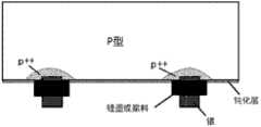
图1是利用P型硅球作为硼源制备局部背场的方法制备的局部背场的示意图。Fig. 1 is a schematic diagram of a local back field prepared by using a P-type silicon sphere as a boron source to prepare a local back field.
the
具体实施方式Detailed ways
以下举例具体实施例对本发明进行说明。需要指出的是,以下实施例只用于对本发明作进一步说明,不代表本发明的保护范围,其他人根据本发明的提示进行的非本质的修改和调整,仍属于本发明的保护范围。The following specific examples are given to illustrate the present invention. It should be pointed out that the following examples are only used to further illustrate the present invention, and do not represent the protection scope of the present invention. Non-essential modifications and adjustments made by others according to the hints of the present invention still belong to the protection scope of the present invention.
the
实施例1Example 1
本实施例提供一种利用P型硅球作为硼源制备局部背场的方法,当采用硅浆料作为原料,运用丝网印刷机印刷图形,具体步骤如下:This embodiment provides a method of using P-type silicon balls as a boron source to prepare a local back field. When using silicon paste as a raw material, a screen printing machine is used to print graphics. The specific steps are as follows:
1) 选用电阻率在0.5~6Ω·cm的轻掺杂的P型单晶硅片,将其置于制绒槽中,在比重为15%的氢氧化钠溶液中,在温度为75~80℃的条件下,进行表面组织化形成绒面结构;1) Choose a lightly doped P-type single crystal silicon wafer with a resistivity of 0.5-6Ω·cm, place it in a texturing tank, and place it in a sodium hydroxide solution with a specific gravity of 15% at a temperature of 75-80 Under the condition of ℃, the surface texture is formed to form a suede structure;
2) 对硅片表面进行化学溶液清洗,溶液为氢氟酸和盐酸的混合溶液,清洗时间为2Min,温度为20~25℃;2) Clean the surface of the silicon wafer with a chemical solution, the solution is a mixed solution of hydrofluoric acid and hydrochloric acid, the cleaning time is 2Min, and the temperature is 20-25°C;
3) 清洗后,将硅片置于扩散炉中,在830~850℃的条件下进行扩散,扩散后方阻70~85Ω/□左右,时间在10~15Min左右;3) After cleaning, place the silicon wafer in a diffusion furnace and carry out diffusion at 830-850°C. After diffusion, the resistance is about 70-85Ω/□, and the time is about 10-15Min;
4) 将上述扩散后的硅片置于湿法刻蚀机中,去除背结和磷硅玻璃;4) Place the diffused silicon wafer in a wet etching machine to remove the back junction and phosphosilicate glass;
5) 在硅片的背面印刷掺硼硅浆料,印刷图案为线状阵列时,线宽120μm,线间距1500μm,印刷厚度为6μm;5) Print borosilicate paste on the back of the silicon wafer. When the printed pattern is a linear array, the line width is 120 μm, the line spacing is 1500 μm, and the printing thickness is 6 μm;
6) 印刷浆料后,进行烘干,烘干温度为300℃,时间2 min;6) After printing the paste, dry it at 300°C for 2 minutes;
7) 退火处理,800℃,峰值保温10 Min,得到带硼掺杂的局部背场;7) Annealing treatment, 800 ° C, peak holding time 10 Min, to obtain a local back field with boron doping;
8) 背面沉积钝化膜;8) Deposit passivation film on the back;
9) 前表面沉积钝化及减反膜;9) Deposit passivation and anti-reflection film on the front surface;
10)背面电极印刷:印刷背电极用于组件焊接;10) Back electrode printing: printed back electrodes are used for component welding;
11)背面银浆印刷:印刷银浆套印在硅浆料印刷的位置,银浆将打开钝化膜形成接触,背银的线宽是100μm;再将银浆烘干,其步骤是:在快速烧结炉或者链式炉中完成,温度为200℃,干燥时间为30s;11) Silver paste printing on the back side: overprint the silver paste on the position where the silicon paste is printed, the silver paste will open the passivation film to form contact, and the line width of the back silver is 100 μm; then dry the silver paste, the steps are: Finish in a sintering furnace or a chain furnace, the temperature is 200°C, and the drying time is 30s;
12)正面电极印刷;12) Front electrode printing;
13)高温快速烧结:将印刷完的硅片置于烧结炉中烧结,烧结温度为780~800℃,峰值温度保温时间3 s,经烧结后正面银电极穿过SiNx减反膜形成欧姆接触。13) High-temperature rapid sintering: place the printed silicon wafer in a sintering furnace for sintering, the sintering temperature is 780-800°C, and the peak temperature holding time is 3 s. After sintering, the front silver electrode passes through the SiNx anti-reflection film to form an ohmic contact.
对制备得到的硅片进行性能测试,P型硅球作为硼源形成的局部背场使得表面复合速率降至125cm/s或更小,少子寿命100μs,背场串联电阻Rs为0.65Ω·cm2,开路电压Voc为650mV,电流密度Jsc为38.1±0.1mA/ cm2,填充因子FF为78.5±0.5%。The performance test of the prepared silicon wafer shows that the local back field formed by P-type silicon balls as a boron source reduces the surface recombination rate to 125cm/s or less, the minority carrier lifetime is 100μs, and the back field series resistance Rs is 0.65Ω·cm2 , the open circuit voltage Voc is 650mV, the current density Jsc is 38.1±0.1mA/cm2 , and the fill factor FF is 78.5±0.5%.
本实施例中,采用的P型硅球作为硼源的参数是:硼掺杂量1.06×10²⁰atoms/cm3,硅球粒径范围是0.5~1.5μm,尺寸集中在0.8μm,集中度大于90%,硅球的制备方法是通过脉冲放电方法制备得到的,脉冲放电的工艺参数是:开路电压120V;峰值电流10A;脉宽50μs;占空比1:2。In this example, the parameters of the P-type silicon spheres used as the boron source are: the doping amount of boron is 1.06×10²⁰ atoms/cm3 , the particle size range of the silicon spheres is 0.5-1.5 μm, the size is concentrated at 0.8 μm, and the concentration More than 90%, the preparation method of silicon balls is obtained by pulse discharge method, and the process parameters of pulse discharge are: open circuit voltage 120V; peak current 10A; pulse width 50μs; duty ratio 1:2.
浆料的质量百分比配方是P型硅球12%,乙醇64.5%,表面活性剂Pluronic F-127 3.5%,聚乙烯吡咯烷酮20%。The mass percent formula of the slurry is 12% of P-type silicon spheres, 64.5% of ethanol, 3.5% of surfactant Pluronic F-127, and 20% of polyvinylpyrrolidone.
本实施例中所述银浆均为量产的产品,本工艺没有引入新设备,在800℃下形成背场局部硼掺杂,降低了表面复合速率,提高了电池的光电转化效率。The silver pastes described in this example are all mass-produced products. No new equipment is introduced in this process. Partial boron doping in the back field is formed at 800° C., which reduces the surface recombination rate and improves the photoelectric conversion efficiency of the battery.
the
实施例2Example 2
本实施例提供一种利用P型硅球作为硼源制备局部背场的方法,当采用硅浆料作为原料,运用丝网印刷机印刷图形,具体步骤如下:This embodiment provides a method of using P-type silicon balls as a boron source to prepare a local back field. When using silicon paste as a raw material, a screen printing machine is used to print graphics. The specific steps are as follows:
1) 选用电阻率在0.5~6Ω·cm的轻掺杂的P型单晶硅片,将其置于制绒槽中,在比重为15%的氢氧化钠溶液中,在温度为75~80℃的条件下,进行表面组织化形成绒面结构;1) Choose a lightly doped P-type single crystal silicon wafer with a resistivity of 0.5-6Ω·cm, place it in a texturing tank, and place it in a sodium hydroxide solution with a specific gravity of 15% at a temperature of 75-80 Under the condition of ℃, the surface texture is formed to form a suede structure;
2) 对硅片表面进行化学溶液清洗,溶液为氢氟酸和盐酸的混合溶液,清洗时间为2Min,温度为20~25℃;2) Clean the surface of the silicon wafer with a chemical solution, the solution is a mixed solution of hydrofluoric acid and hydrochloric acid, the cleaning time is 2Min, and the temperature is 20-25°C;
3) 清洗后,将硅片置于扩散炉中,在830~850℃的条件下进行扩散,扩散后方阻70~85Ω/□左右,时间在10~15Min左右;3) After cleaning, place the silicon wafer in a diffusion furnace and carry out diffusion at 830-850°C. After diffusion, the resistance is about 70-85Ω/□, and the time is about 10-15Min;
4) 将上述扩散后的硅片置于湿法刻蚀机中,去除背结和磷硅玻璃;4) Place the diffused silicon wafer in a wet etching machine to remove the back junction and phosphosilicate glass;
5) 在硅片的背面印刷掺硼硅浆料,印刷图案为点状阵列,点直径70μm,中心间距100μm,印刷厚度为1μm;5) Print borosilicate paste on the back of the silicon wafer, the printing pattern is a dot array, the dot diameter is 70 μm, the center distance is 100 μm, and the printing thickness is 1 μm;
6) 印刷浆料后,进行烘干,烘干温度为200℃,时间10Min;6) After printing the paste, dry it at 200°C for 10 minutes;
7) 退火处理,750℃,峰值保温15 Min:得到带硼掺杂的局部背场;7) Annealing treatment, 750 ° C, peak holding time 15 Min: to obtain a local back field with boron doping;
8) 背面沉积钝化膜;8) Deposit passivation film on the back;
9) 前表面沉积钝化及减反膜;9) Deposit passivation and anti-reflection film on the front surface;
10)背面电极印刷:印刷背电极用于组件焊接;10) Back electrode printing: printed back electrodes are used for component welding;
11)背面银浆印刷:印刷银浆套印在硅浆料印刷的位置,银浆将打开钝化膜形成接触,背银的点直径是60μm;再将银浆烘干,其步骤是:在快速烧结炉或者链式炉中完成,温度为180℃,干燥时间为60s;11) Silver paste printing on the back side: printing silver paste is overprinted on the position where the silicon paste is printed, the silver paste will open the passivation film to form contact, and the dot diameter of the back silver is 60 μm; then dry the silver paste, the steps are: Finish in a sintering furnace or a chain furnace, the temperature is 180°C, and the drying time is 60s;
12)正面电极印刷;12) Front electrode printing;
13)高温快速烧结:将印刷完的硅片置于烧结炉中烧结,烧结温度为750~780℃,峰值温度保温时间10 s,经烧结后正面银电极穿过SiNx减反膜形成欧姆接触。13) High-temperature rapid sintering: place the printed silicon wafer in a sintering furnace for sintering, the sintering temperature is 750-780°C, and the peak temperature holding time is 10 s. After sintering, the front silver electrode passes through the SiNx anti-reflection film to form an ohmic contact.
对制备得到的硅片进行性能测试,P型硅球作为硼源形成的局部背场使得表面复合速率降至75cm/s或更小,少子寿命500μs,背场串联电阻Rs为0.6Ω·cm2,开路电压Voc为660mV,电流密度Jsc为37.8±0.1mA/ cm2,填充因子FF为78.3±0.5%。The performance test of the prepared silicon wafer shows that the local back field formed by the P-type silicon ball as a boron source reduces the surface recombination rate to 75cm/s or less, the minority carrier lifetime is 500μs, and the back field series resistance Rs is 0.6Ω·cm2 , the open circuit voltage Voc is 660mV, the current density Jsc is 37.8±0.1mA/cm2 , and the fill factor FF is 78.3±0.5%.
本实施例中,采用的P型硅球作为硼源的参数是:硼掺杂量5.65×10¹⁹atoms/cm3,硅球粒径范围是0.1~0.5μm,尺寸集中在0.2μm,集中度大于90%,硅球的制备方法是通过脉冲放电方法制备得到的,脉冲放电的工艺参数是:开路电压100V;峰值电流5A;脉宽20μs;占空比1:1。In this example, the parameters of the P-type silicon spheres used as the boron source are: the doping amount of boron is 5.65×10¹⁹ atoms/cm3 , the particle size range of silicon spheres is 0.1-0.5 μm, the size is concentrated at 0.2 μm, and the concentration More than 90%, the preparation method of silicon spheres is obtained by pulse discharge method. The process parameters of pulse discharge are: open circuit voltage 100V; peak current 5A; pulse width 20μs; duty ratio 1:1.
浆料的质量百分比配方是P型硅球5%,去离子水50%,司盘(80)10%,聚乙烯吡咯烷酮35%。The mass percentage formula of the slurry is 5% of P-type silicon balls, 50% of deionized water, 10% of Span (80), and 35% of polyvinylpyrrolidone.
本实施例中所述银浆均为量产的产品,本工艺没有引入新设备,在750℃下形成背场局部硼掺杂,提高了少子寿命,降低了表面复合速率,提高了电池的光电转化效率。The silver pastes described in this example are all mass-produced products. This process does not introduce new equipment, and local boron doping in the back field is formed at 750°C, which improves the minority carrier lifetime, reduces the surface recombination rate, and improves the photoelectricity of the battery. Conversion efficiency.
the
实施例3Example 3
本实施例提供一种利用P型硅球作为硼源制备局部背场的方法,当采用硅浆料作为原料,运用丝网印刷机印刷图形,具体步骤如下:This embodiment provides a method of using P-type silicon balls as a boron source to prepare a local back field. When using silicon paste as a raw material, a screen printing machine is used to print graphics. The specific steps are as follows:
1) 选用电阻率在1~3Ω·cm的P型多晶硅片,将其置于制绒槽中,在氢氟酸-硝酸(1:6)混合溶液中,在温度为6~10℃,时间110~130S的条件下,进行表面组织化形成绒面结构;1) Select a P-type polysilicon wafer with a resistivity of 1-3Ω·cm, place it in a texturing tank, and place it in a mixed solution of hydrofluoric acid-nitric acid (1:6) at a temperature of 6-10°C for a period of time Under the condition of 110-130S, the surface texture is formed to form a suede structure;
2) 对硅片表面进行化学溶液清洗,溶液分别为2.4%氢氧化钾和5~10%盐酸的混合溶液,清洗时间共为5Min,温度为20~25℃;2) Clean the surface of the silicon wafer with a chemical solution, the solution is a mixed solution of 2.4% potassium hydroxide and 5-10% hydrochloric acid, the cleaning time is 5Min, and the temperature is 20-25°C;
3) 清洗后,将硅片置于扩散炉中,在830~850℃的条件下进行扩散,扩散后方阻70~85Ω/□左右,时间在10~15Min左右;3) After cleaning, place the silicon wafer in a diffusion furnace and carry out diffusion at 830-850°C. After diffusion, the resistance is about 70-85Ω/□, and the time is about 10-15Min;
4) 将上述扩散后的硅片置于湿法刻蚀机中,去除背结和磷硅玻璃;4) Place the diffused silicon wafer in a wet etching machine to remove the back junction and phosphosilicate glass;
5) 在硅片的背面印刷掺硼硅浆料,印刷图案为线状阵列,线宽120μm,线间距2000μm,印刷厚度为12μm;5) Print borosilicate paste on the back of the silicon wafer, the printing pattern is a linear array, the line width is 120 μm, the line spacing is 2000 μm, and the printing thickness is 12 μm;
6) 印刷浆料后,进行烘干,烘干温度为300℃,时间2Min;6) After printing the paste, dry it at 300°C for 2 minutes;
7) 退火处理,850℃,峰值保温20 Min:得到带硼掺杂的局部背场;7) Annealing treatment, 850 ° C, peak holding time 20 Min: to obtain a local back field with boron doping;
8) 背面沉积钝化膜;8) Deposit passivation film on the back;
9) 前表面沉积钝化及减反膜;9) Deposit passivation and anti-reflection film on the front surface;
10)背面电极印刷:印刷背电极用于组件焊接;10) Back electrode printing: printed back electrodes are used for component welding;
11)背面银浆印刷:印刷银浆套印在硅浆料印刷的位置,银浆将打开钝化膜形成接触,背银的线宽是110 μm;再将银浆烘干,其步骤是:在快速烧结炉或者链式炉中完成,温度为200℃,干燥时间为40s;11) Silver paste printing on the back side: Print the silver paste overprinted on the position where the silicon paste is printed, the silver paste will open the passivation film to form contact, the line width of the back silver is 110 μm; then dry the silver paste, the steps are: Complete in a rapid sintering furnace or a chain furnace, the temperature is 200°C, and the drying time is 40s;
12)正面电极印刷;12) Front electrode printing;
13)高温快速烧结:将印刷完的硅片置于烧结炉中烧结,烧结温度为810~830℃,峰值温度保温时间3 s,经烧结后正面银电极穿过SiNx减反膜形成欧姆接触。13) High-temperature rapid sintering: place the printed silicon wafer in a sintering furnace for sintering, the sintering temperature is 810-830°C, and the peak temperature holding time is 3 s. After sintering, the front silver electrode passes through the SiNx anti-reflection film to form an ohmic contact.
对制备得到的硅片进行性能测试,P型硅球作为硼源形成的局部背场使得表面复合速率降至155cm/s或更小,少子寿命150μs,背场串联电阻Rs为0.68Ω·cm2,开路电压Voc为625mV,电流密度Jsc为38.2±0.1mA/ cm2,填充因子FF为77.9±0.5%。The performance test of the prepared silicon wafer shows that the local back field formed by the P-type silicon ball as a boron source reduces the surface recombination rate to 155cm/s or less, the minority carrier lifetime is 150μs, and the back field series resistance Rs is 0.68Ω·cm2 , the open circuit voltage Voc is 625mV, the current density Jsc is 38.2±0.1mA/cm2 , and the fill factor FF is 77.9±0.5%.
本实施例中,采用的P型硅球作为硼源的参数是:硼掺杂量4.63×10¹⁹atoms/cm3,硅球粒径范围是0.5~2μm,尺寸集中在1μm,集中度大于90%,硅球的制备方法是通过脉冲放电方法制备得到的,脉冲放电的工艺参数是:开路电压150V;峰值电流10A;脉宽30μs;占空比2:1。In this example, the parameters of the P-type silicon spheres used as the boron source are: the doping amount of boron is 4.63×10¹⁹ atoms/cm3 , the particle size range of the silicon spheres is 0.5-2 μm, the size is concentrated at 1 μm, and the concentration is greater than 90. %, the preparation method of silicon balls is obtained by pulse discharge method, and the process parameters of pulse discharge are: open circuit voltage 150V; peak current 10A; pulse width 30μs; duty ratio 2:1.
浆料的质量百分比配方是P型硅球20%,乙醇69%,AEO-9含量1%,聚乙二醇10%。The mass percentage formula of the slurry is 20% of P-type silicon spheres, 69% of ethanol, 1% of AEO-9 content, and 10% of polyethylene glycol.
本实施例中所述银浆均为量产的产品,本工艺没有引入新设备,在850℃下形成背场局部硼掺杂,降低了表面复合速率,提高了电池的光电转化效率。The silver pastes described in this example are all mass-produced products. This process does not introduce new equipment, and local boron doping in the back field is formed at 850° C., which reduces the surface recombination rate and improves the photoelectric conversion efficiency of the battery.
the
实施例4Example 4
本实施例提供一种利用P型硅球作为硼源制备局部背场的方法,当采用硅浆料作为原料,运用丝网印刷机印刷图形,具体步骤如下:This embodiment provides a method of using P-type silicon balls as a boron source to prepare a local back field. When using silicon paste as a raw material, a screen printing machine is used to print graphics. The specific steps are as follows:
1) 选用电阻率在1~3Ω·cm的P型多晶硅片,将其置于制绒槽中,在氢氟酸-硝酸(1:6)混合溶液中,在温度为6~10℃,时间110~130S的条件下,进行表面组织化形成绒面结构;1) Select a P-type polysilicon wafer with a resistivity of 1-3Ω·cm, place it in a texturing tank, and place it in a mixed solution of hydrofluoric acid-nitric acid (1:6) at a temperature of 6-10°C for a period of time Under the condition of 110-130S, the surface texture is formed to form a suede structure;
2) 对硅片表面进行化学溶液清洗,溶液分别为2.4%氢氧化钾和5~10%盐酸的混合溶液,清洗时间共为5Min,温度为20~25℃;2) Clean the surface of the silicon wafer with a chemical solution, the solution is a mixed solution of 2.4% potassium hydroxide and 5-10% hydrochloric acid, the cleaning time is 5Min, and the temperature is 20-25°C;
3) 清洗后,将硅片置于扩散炉中,在830~850℃的条件下进行扩散,扩散后方阻70~85Ω/□左右,时间在10~15Min左右;3) After cleaning, place the silicon wafer in a diffusion furnace and carry out diffusion at 830-850°C. After diffusion, the resistance is about 70-85Ω/□, and the time is about 10-15Min;
4) 将上述扩散后的硅片置于湿法刻蚀机中,去除背结和磷硅玻璃;4) Place the diffused silicon wafer in a wet etching machine to remove the back junction and phosphosilicate glass;
5) 在硅片的背面印刷掺硼硅浆料,印刷图案为点状阵列,点直径150μm,中心间距1200μm,印刷厚度为10μm;5) Print borosilicate paste on the back of the silicon wafer, the printing pattern is a dot array, the dot diameter is 150 μm, the center distance is 1200 μm, and the printing thickness is 10 μm;
6) 印刷浆料后,进行烘干,烘干温度为300℃,时间2Min;6) After printing the paste, dry it at 300°C for 2 minutes;
7) 退火处理,900℃,峰值保温20 Min:得到带硼掺杂的局部背场;7) Annealing treatment, 900 ° C, peak holding time 20 Min: get a local back field with boron doping;
8) 背面沉积钝化膜;8) Deposit passivation film on the back;
9) 前表面沉积钝化及减反膜;9) Deposit passivation and anti-reflection film on the front surface;
10)背面电极印刷:印刷背电极用于组件焊接;10) Back electrode printing: printed back electrodes are used for component welding;
11)背面银浆印刷:印刷银浆套印在硅浆料印刷的位置,银浆将打开钝化膜形成接触,背银的点直径是100 μm;再将银浆烘干,其步骤是:在快速烧结炉或者链式炉中完成,温度为300℃,干燥时间为10s;11) Silver paste printing on the back side: Print the silver paste overprinted on the position where the silicon paste is printed, the silver paste will open the passivation film to form contact, the dot diameter of the back silver is 100 μm; then dry the silver paste, the steps are: Complete in a rapid sintering furnace or a chain furnace, the temperature is 300°C, and the drying time is 10s;
12)正面电极印刷;12) Front electrode printing;
13)高温快速烧结:将印刷完的硅片置于烧结炉中烧结,烧结温度为820~850℃,峰值温度保温时间1 s,经烧结后正面银电极穿过SiNx减反膜形成欧姆接触。13) High-temperature rapid sintering: place the printed silicon wafer in a sintering furnace for sintering, the sintering temperature is 820-850°C, and the peak temperature holding time is 1 s. After sintering, the front silver electrode passes through the SiNx anti-reflection film to form an ohmic contact.
对制备得到的硅片进行性能测试,P型硅球作为硼源形成的局部背场使得表面复合速率降至220cm/s或更小,少子寿命100μs,背场串联电阻Rs为0.77Ω·cm2,开路电压Voc为610mV,电流密度Jsc为37.0±0.1mA/ cm2,填充因子FF为77.2±0.5%。The performance test of the prepared silicon wafer shows that the local back field formed by P-type silicon spheres as a boron source reduces the surface recombination rate to 220cm/s or less, the minority carrier lifetime is 100μs, and the back field series resistance Rs is 0.77Ω·cm2 , the open circuit voltage Voc is 610mV, the current density Jsc is 37.0±0.1mA/cm2 , and the fill factor FF is 77.2±0.5%.
本实施例中,采用的P型硅球作为硼源的参数是:硼掺杂量5.65×10¹⁹atoms/cm3,硅球粒径范围是0.8~3μm,尺寸集中在1.5μm,集中度大于90%,硅球的制备方法是通过脉冲放电方法制备得到的,脉冲放电的工艺参数是:开路电压150V;峰值电流15A;脉宽50μs;占空比2:1。In this example, the parameters of the P-type silicon spheres used as the boron source are: the doping amount of boron is 5.65×10¹⁹ atoms/cm3 , the particle size range of the silicon spheres is 0.8-3 μm, the size is concentrated at 1.5 μm, and the concentration is greater than 90%, the preparation method of silicon balls is obtained by pulse discharge method, and the process parameters of pulse discharge are: open circuit voltage 150V; peak current 15A; pulse width 50μs; duty ratio 2:1.
浆料的质量百分比配方是P型硅球5.5%,苯80%,TX-10 2%,聚乙烯吡咯烷酮12.5%。The mass percent formula of the slurry is 5.5% of P-type silicon balls, 80% of benzene, 2% of TX-10, and 12.5% of polyvinylpyrrolidone.
本实施例中所述银浆均为量产的产品,本工艺没有引入新设备,在900℃下形成背场局部硼掺杂,降低了表面复合速率,提高了电池的光电转化效率。The silver pastes described in this example are all mass-produced products. No new equipment is introduced in this process, and local boron doping in the back field is formed at 900° C., which reduces the surface recombination rate and improves the photoelectric conversion efficiency of the battery.
the
实施例5Example 5
本实施例提供一种利用P型硅球作为硼源制备局部背场的方法,采用硅墨作为原料,运用喷墨打印机打印图形,具体步骤如下:This embodiment provides a method for preparing a local back field using P-type silicon spheres as a boron source, using silicon ink as a raw material, and using an inkjet printer to print graphics. The specific steps are as follows:
1) 选用电阻率在0.5~6Ω·cm的轻掺杂的P型单晶硅片,将其置于制绒槽中,在比重为15%的氢氧化钠溶液中,在温度为80~85℃的条件下,进行表面组织化形成绒面结构;1) Select a lightly doped P-type single crystal silicon wafer with a resistivity of 0.5-6Ω·cm, place it in a texturing tank, and place it in a sodium hydroxide solution with a specific gravity of 15% at a temperature of 80-85 Under the condition of ℃, the surface texture is formed to form a suede structure;
2) 对硅片表面进行化学溶液清洗,溶液为氢氟酸和盐酸的混合溶液,清洗时间为2Min,温度为20~25℃;2) Clean the surface of the silicon wafer with a chemical solution, the solution is a mixed solution of hydrofluoric acid and hydrochloric acid, the cleaning time is 2Min, and the temperature is 20-25°C;
3) 清洗后,将硅片置于扩散炉中,在830~850℃的条件下进行扩散,扩散后方阻70~85Ω/□左右,时间在10~15Min左右;3) After cleaning, place the silicon wafer in a diffusion furnace and carry out diffusion at 830-850°C. After diffusion, the resistance is about 70-85Ω/□, and the time is about 10-15Min;
4) 将上述扩散后的硅片置于湿法刻蚀机中,去除背结和磷硅玻璃;4) Place the diffused silicon wafer in a wet etching machine to remove the back junction and phosphosilicate glass;
5) 在硅片的背面喷墨打印硅墨,打印图案为线状阵列时,线宽200μm,线间距1500μm,打印厚度为0.5μm;5) Silicon ink is inkjet printed on the back of the silicon wafer. When the printed pattern is a linear array, the line width is 200 μm, the line spacing is 1500 μm, and the printing thickness is 0.5 μm;
6) 打印硅墨后,进行烘干,烘干温度为280℃,时间4 min;6) After printing the silicon ink, dry it at 280°C for 4 minutes;
7) 退火处理,780℃,峰值保温时间约15 min:得到带硼掺杂的局部背场;7) Annealing treatment, 780 ° C, peak holding time of about 15 min: to obtain a local back field with boron doping;
8) 背面沉积钝化膜;8) Deposit passivation film on the back;
9) 前表面沉积钝化及减反膜;9) Deposit passivation and anti-reflection film on the front surface;
10)背面电极印刷:印刷背电极用于组件焊接;10) Back electrode printing: printed back electrodes are used for component welding;
11)背面银浆印刷:印刷银浆套印在硅浆料印刷的位置,银浆将打开钝化膜形成接触,背银线宽范围可以是80μm,间距和印浆间距相同,将银浆烘干,温度为200℃,干燥时间为30s;11) Silver paste printing on the back side: the printing silver paste is overprinted at the position where the silicon paste is printed, the silver paste will open the passivation film to form contact, the back silver line width can be 80μm, the spacing is the same as the printing paste spacing, and the silver paste is dried , the temperature is 200°C, and the drying time is 30s;
12)正面电极印刷;12) Front electrode printing;
13)高温快速烧结:将印刷完的硅片置于烧结炉中烧结,烧结温度为780~800℃,峰值温度保温时间5s,经烧结后正面银电极穿过SiNx减反膜形成欧姆接触。13) High-temperature rapid sintering: place the printed silicon wafer in a sintering furnace for sintering, the sintering temperature is 780-800°C, and the peak temperature holding time is 5s. After sintering, the front silver electrode passes through the SiNx anti-reflection film to form an ohmic contact.
对制备得到的硅片进行性能测试,P型硅球作为硼源形成的局部背场使得表面复合速率降至60cm/s或更小,少子寿命1000μs,背场串联电阻Rs为0.58Ω·cm2,开路电压Voc为658mV,电流密度Jsc为38.4±0.1mA/ cm2,填充因子FF为78.9±0.6%。The performance test of the prepared silicon wafer shows that the local back field formed by P-type silicon spheres as a boron source reduces the surface recombination rate to 60cm/s or less, the minority carrier lifetime is 1000μs, and the back field series resistance Rs is 0.58Ω·cm2 , the open circuit voltage Voc is 658mV, the current density Jsc is 38.4±0.1mA/cm2 , and the fill factor FF is 78.9±0.6%.
本实施例中,采用的P型硅球作为硼源的参数是:硼掺杂量1.06×10²⁰atoms/cm3,硅球粒径范围是50nm~250nm,尺寸集中在80nm,集中度大于90%,硅球的制备方法是通过脉冲放电方法制备得到的,脉冲放电的工艺参数是:开路电压120V;峰值电流5A;脉宽20μs ;占空比1:2。In this embodiment, the parameters of the P-type silicon spheres used as the boron source are: the boron doping amount is 1.06×10²⁰ atoms/cm3 , the particle size range of the silicon spheres is 50nm to 250nm, the size is concentrated at 80nm, and the concentration is greater than 90. %, the preparation method of silicon balls is prepared by pulse discharge method, and the process parameters of pulse discharge are: open circuit voltage 120V; peak current 5A; pulse width 20μs; duty ratio 1:2.
硅墨的质量百分比配方是P型硅球5%,去离子水88%,Pluronic F-127 3.5%,聚乙二醇3.5%。The mass percentage formula of silicon ink is P-type silicon ball 5%, deionized water 88%, Pluronic F-127 3.5%, polyethylene glycol 3.5%.
本实施例中所述银浆均为量产的产品,仅添加一台喷墨打印机,在780℃下形成背场局部硼掺杂,提高了少子寿命,降低了表面复合速率,提高了电池的光电转化效率。相对于实施例中的线性阵列,优化过的点阵可以获得更好的背面钝化效果。The silver pastes described in this example are all mass-produced products. Only one inkjet printer is added to form local boron doping in the back field at 780°C, which improves the minority carrier lifetime, reduces the surface recombination rate, and improves the battery life. Photoelectric conversion efficiency. Compared with the linear array in the embodiment, the optimized dot matrix can obtain a better rear passivation effect.
the
实施例6Example 6
本实施例提供一种利用P型硅球作为硼源制备局部背场的方法,采用硅墨作为原料,运用喷墨打印机打印图形,具体步骤如下:This embodiment provides a method for preparing a local back field using P-type silicon spheres as a boron source, using silicon ink as a raw material, and using an inkjet printer to print graphics. The specific steps are as follows:
1) 选用电阻率在0.5~6Ω·cm的轻掺杂的P型单晶硅片,将其置于制绒槽中,在比重为15%的氢氧化钠溶液中,在温度为80~85℃的条件下,进行表面组织化形成绒面结构;1) Select a lightly doped P-type single crystal silicon wafer with a resistivity of 0.5-6Ω·cm, place it in a texturing tank, and place it in a sodium hydroxide solution with a specific gravity of 15% at a temperature of 80-85 Under the condition of ℃, the surface texture is formed to form a suede structure;
2) 对硅片表面进行化学溶液清洗,溶液为氢氟酸和盐酸的混合溶液,清洗时间为2Min,温度为20~25℃;2) Clean the surface of the silicon wafer with a chemical solution, the solution is a mixed solution of hydrofluoric acid and hydrochloric acid, the cleaning time is 2Min, and the temperature is 20-25°C;
3) 清洗后,将硅片置于扩散炉中,在830~850℃的条件下进行扩散,扩散后方阻70~85Ω/□左右,时间在10~15Min左右;3) After cleaning, place the silicon wafer in a diffusion furnace and carry out diffusion at 830-850°C. After diffusion, the resistance is about 70-85Ω/□, and the time is about 10-15Min;
4) 将上述扩散后的硅片置于湿法刻蚀机中,去除背结和磷硅玻璃;4) Place the diffused silicon wafer in a wet etching machine to remove the back junction and phosphosilicate glass;
5) 在硅片的背面喷墨打印硅墨,打印图案为点状阵列,点直径250μm,中心间距2000μm,打印厚度为5μm;5) Inkjet printing silicon ink on the back of the silicon wafer, the printing pattern is a dot array, the dot diameter is 250 μm, the center distance is 2000 μm, and the printing thickness is 5 μm;
6) 打印硅墨后,进行烘干,烘干温度为350℃,时间1 min;6) After printing the silicon ink, dry it at 350°C for 1 min;
7) 退火处理,850℃,峰值保温时间约5 min:得到带硼掺杂的局部背场;7) Annealing treatment, 850°C, peak holding time about 5 minutes: get a local back field with boron doping;
8) 背面沉积钝化膜;8) Deposit passivation film on the back;
9) 前表面沉积钝化及减反膜;9) Deposit passivation and anti-reflection film on the front surface;
10)背面电极印刷:印刷背电极用于组件焊接;10) Back electrode printing: printed back electrodes are used for component welding;
11)背面银浆印刷:印刷银浆套印在硅浆料印刷的位置,背银的点直径为110μm,间距和印浆间距相同,将银浆烘干,烘干工艺是:温度为300℃,干燥时间为10s,银浆将打开钝化膜形成接触;11) Silver paste printing on the back side: the printing silver paste is overprinted at the position where the silicon paste is printed, the dot diameter of the back silver is 110 μm, and the spacing is the same as that of the printing paste, and the silver paste is dried. The drying process is: the temperature is 300 ° C, The drying time is 10s, and the silver paste will open the passivation film to form contact;
12)正面电极印刷;12) Front electrode printing;
13)高温快速烧结:将印刷完的硅片置于烧结炉中烧结,烧结温度为840~850℃,峰值温度保温时间是1 s,经烧结后正面银电极穿过SiNx减反膜形成欧姆接触。13) High-temperature rapid sintering: place the printed silicon wafer in a sintering furnace for sintering, the sintering temperature is 840-850°C, and the peak temperature holding time is 1 s. After sintering, the front silver electrode passes through the SiNx anti-reflection film to form an ohmic contact .
对制备得到的硅片进行性能测试,P型硅球作为硼源形成的局部背场使得表面复合速率降至65cm/s或更小,少子寿命500μs,背场串联电阻Rs为0.7Ω·cm2,开路电压Voc为630mV,电流密度Jsc为38.1±0.1mA/ cm2,填充因子FF为78.1±0.6%。The performance test of the prepared silicon wafer shows that the local back field formed by the P-type silicon ball as a boron source reduces the surface recombination rate to 65cm/s or less, the minority carrier lifetime is 500μs, and the back field series resistance Rs is 0.7Ω·cm2 , the open circuit voltage Voc is 630mV, the current density Jsc is 38.1±0.1mA/cm2 , and the fill factor FF is 78.1±0.6%.
本实施例中,采用的P型硅球作为硼源的参数是:硼掺杂量1.06×10²⁰atoms/cm3,硅球粒径范围是200nm~500nm,尺寸集中在350nm,集中度大于90%,硅球的制备方法是通过脉冲放电方法制备得到的,脉冲放电的工艺参数是:开路电压120V;峰值电流10A;脉宽50μs ;占空比2:1。In this example, the parameters of the P-type silicon spheres used as the boron source are: the doping amount of boron is 1.06×10²⁰ atoms/cm3 , the particle size range of the silicon spheres is 200nm to 500nm, the size is concentrated at 350nm, and the concentration is greater than 90. %, the preparation method of silicon balls is prepared by pulse discharge method, and the process parameters of pulse discharge are: open circuit voltage 120V; peak current 10A; pulse width 50μs; duty ratio 2:1.
硅墨的质量百分比配方是掺硼硅球2%,二氯甲烷80%,TX-10 10%,聚乙烯吡咯烷酮8%。The mass percentage formula of silicon ink is borosilicate ball 2%, methylene chloride 80%, TX-10 10%, polyvinylpyrrolidone 8%.
本实施例中所述银浆均为量产的产品,仅添加一台喷墨打印机,在850℃下形成背场局部硼掺杂,提高了少子寿命,降低了表面复合速率,提高了电池的光电转化效率。相对于实施例中的线性阵列,优化过的点阵可以获得更好的背面钝化效果。The silver pastes described in this example are all mass-produced products. Only one inkjet printer is added to form local boron doping in the back field at 850°C, which improves the minority carrier lifetime, reduces the surface recombination rate, and improves the battery life. Photoelectric conversion efficiency. Compared with the linear array in the embodiment, the optimized dot matrix can obtain a better rear passivation effect.
the
实施例7Example 7
本实施例提供一种利用P型硅球作为硼源制备局部背场的方法,采用硅墨作为原料,运用喷墨打印机打印图形,具体步骤如下:This embodiment provides a method for preparing a local back field using P-type silicon spheres as a boron source, using silicon ink as a raw material, and using an inkjet printer to print graphics. The specific steps are as follows:
1) 选用电阻率在1~3Ω·cm的P型多晶硅片,将其置于制绒槽中,在氢氟酸-硝酸(1:6)混合溶液中,在温度为6~10℃,时间110~130S的条件下,进行表面组织化形成绒面结构;1) Select a P-type polysilicon wafer with a resistivity of 1-3Ω·cm, place it in a texturing tank, and place it in a mixed solution of hydrofluoric acid-nitric acid (1:6) at a temperature of 6-10°C for a period of time Under the condition of 110-130S, the surface texture is formed to form a suede structure;
2) 对硅片表面进行化学溶液清洗,溶液分别为2.4%氢氧化钾和5~10%盐酸的混合溶液,清洗时间共为5Min,温度为20~25℃;2) Clean the surface of the silicon wafer with a chemical solution, the solution is a mixed solution of 2.4% potassium hydroxide and 5-10% hydrochloric acid, the cleaning time is 5Min, and the temperature is 20-25°C;
3) 清洗后,将硅片置于扩散炉中,在830~850℃的条件下进行扩散,扩散后方阻70~85Ω/□左右,时间在10~15Min左右;3) After cleaning, place the silicon wafer in a diffusion furnace and carry out diffusion at 830-850°C. After diffusion, the resistance is about 70-85Ω/□, and the time is about 10-15Min;
4) 将上述扩散后的硅片置于湿法刻蚀机中,去除背结和磷硅玻璃;4) Place the diffused silicon wafer in a wet etching machine to remove the back junction and phosphosilicate glass;
5) 在硅片的背面喷墨打印硅墨,打印图案为线状阵列时,线宽70μm,线间距1500μm,打印厚度为2μm;5) Silicon ink is inkjet printed on the back of the silicon wafer. When the printed pattern is a linear array, the line width is 70 μm, the line spacing is 1500 μm, and the printing thickness is 2 μm;
6) 打印硅墨后,进行烘干,烘干温度为200℃,时间8 min;6) After printing the silicon ink, dry it at 200°C for 8 minutes;
7) 退火处理,800℃,峰值保温时间约30 min:得到带硼掺杂的局部背场;7) Annealing treatment, 800°C, peak holding time about 30 minutes: get a local back field with boron doping;
8) 背面沉积钝化膜;8) Deposit passivation film on the back;
9) 前表面沉积钝化及减反膜;9) Deposit passivation and anti-reflection film on the front surface;
10)背面电极印刷:印刷背电极用于组件焊接;10) Back electrode printing: printed back electrodes are used for component welding;
11)背面银浆印刷:印刷银浆套印在硅浆料印刷的位置,背银的线宽是50μm,间距和印浆间距相同,银浆烘干的工艺是:烘干温度180℃,烘干时间60s,银浆将打开钝化膜形成接触;11) Silver paste printing on the back side: the printing silver paste is overprinted at the position where the silicon paste is printed, the line width of the back silver is 50 μm, and the spacing is the same as that of the printing paste. The drying process of the silver paste is: drying temperature 180°C, drying Time 60s, the silver paste will open the passivation film to form contact;
12)正面电极印刷;12) Front electrode printing;
13)高温快速烧结:将印刷完的硅片置于烧结炉中烧结,烧结温度为780~800℃,峰值温度保温时间是3 s,经烧结后正面银电极穿过SiNx减反膜形成欧姆接触。13) High-temperature rapid sintering: place the printed silicon wafer in a sintering furnace for sintering, the sintering temperature is 780-800°C, and the peak temperature holding time is 3 s. After sintering, the front silver electrode passes through the SiNx anti-reflection film to form an ohmic contact .
对制备得到的硅片进行性能测试,P型硅球作为硼源形成的局部背场使得表面复合速率降至120cm/s或更小,少子寿命100μs,背场串联电阻Rs为0.72Ω·cm2,开路电压Voc为620mV,电流密度Jsc为37.8±0.1mA/ cm2,填充因子FF为77.5±0.6%。The performance test of the prepared silicon wafer shows that the local back field formed by P-type silicon spheres as a boron source reduces the surface recombination rate to 120cm/s or less, the minority carrier lifetime is 100μs, and the back field series resistance Rs is 0.72Ω·cm2 , the open circuit voltage Voc is 620mV, the current density Jsc is 37.8±0.1mA/cm2 , and the fill factor FF is 77.5±0.6%.
本实施例中,采用的P型硅球作为硼源的参数是:硼掺杂量2.01×10¹⁹atoms/cm3,硅球粒径范围是100nm~400nm,尺寸集中在250nm,集中度大于90%,硅球的制备方法是通过脉冲放电方法制备得到的,脉冲放电的工艺参数是:开路电压150V;峰值电流10A;脉宽30μs ;占空比1:1。In this example, the parameters of the P-type silicon spheres used as the boron source are: the boron doping amount is 2.01×10¹⁹ atoms/cm3 , the particle size range of the silicon spheres is 100nm to 400nm, the size is concentrated at 250nm, and the concentration is greater than 90. %, the preparation method of silicon balls is prepared by pulse discharge method, and the process parameters of pulse discharge are: open circuit voltage 150V; peak current 10A; pulse width 30μs; duty ratio 1:1.
硅墨的质量百分比配方是P型硅球10%,去离子水88.5%,Pluronic F-127 0.5%,聚乙二醇1%。The mass percentage formula of silicon ink is P-type silicon ball 10%, deionized water 88.5%, Pluronic F-127 0.5%, polyethylene glycol 1%.
本实施例中所述银浆均为量产的产品,仅添加一台喷墨打印机,在800℃下形成背场局部硼掺杂,提高了少子寿命,降低了表面复合速率,提高了电池的光电转化效率。相对于实施例中的线性阵列,优化过的点阵可以获得更好的背面钝化效果。The silver pastes described in this example are all mass-produced products. Only one inkjet printer is added to form local boron doping in the back field at 800°C, which improves the minority carrier lifetime, reduces the surface recombination rate, and improves the battery life. Photoelectric conversion efficiency. Compared with the linear array in the embodiment, the optimized dot matrix can obtain a better rear passivation effect.
the
实施例8Example 8
本实施例提供一种利用P型硅球作为硼源制备局部背场的方法,采用硅墨作为原料,运用喷墨打印机打印图形,具体步骤如下:This embodiment provides a method for preparing a local back field using P-type silicon spheres as a boron source, using silicon ink as a raw material, and using an inkjet printer to print graphics. The specific steps are as follows:
1) 选用电阻率在1~3Ω·cm的P型多晶硅片,将其置于制绒槽中,在氢氟酸-硝酸(1:6)混合溶液中,在温度为6~10℃,时间110~130S的条件下,进行表面组织化形成绒面结构;1) Select a P-type polysilicon wafer with a resistivity of 1-3Ω·cm, place it in a texturing tank, and place it in a mixed solution of hydrofluoric acid-nitric acid (1:6) at a temperature of 6-10°C for a period of time Under the condition of 110-130S, the surface texture is formed to form a suede structure;
2) 对硅片表面进行化学溶液清洗,溶液分别为2.4%氢氧化钾和5~10%盐酸的混合溶液,清洗时间共为5Min,温度为20~25℃;2) Clean the surface of the silicon wafer with a chemical solution, the solution is a mixed solution of 2.4% potassium hydroxide and 5-10% hydrochloric acid, the cleaning time is 5Min, and the temperature is 20-25°C;
3) 清洗后,将硅片置于扩散炉中,在830~850℃的条件下进行扩散,扩散后方阻70~85Ω/□左右,时间在10~15Min左右;3) After cleaning, place the silicon wafer in a diffusion furnace and carry out diffusion at 830-850°C. After diffusion, the resistance is about 70-85Ω/□, and the time is about 10-15Min;
4) 将上述扩散后的硅片置于湿法刻蚀机中,去除背结和磷硅玻璃;4) Place the diffused silicon wafer in a wet etching machine to remove the back junction and phosphosilicate glass;
5) 在硅片的背面喷墨打印硅墨,打印图案为点状阵列,点直径120μm,中心间距1200μm,打印厚度为3μm;5) Inkjet printing silicon ink on the back of the silicon wafer, the printing pattern is a dot array, the dot diameter is 120 μm, the center distance is 1200 μm, and the printing thickness is 3 μm;
6) 打印硅墨后,进行烘干,烘干温度为280℃,时间1 min;6) After printing the silicon ink, dry it at 280°C for 1 min;
7) 退火处理,750℃,峰值保温时间约15 min,得到带硼掺杂的局部背场;7) Annealing treatment, 750°C, peak holding time of about 15 minutes, to obtain a local back field with boron doping;
8) 背面沉积钝化膜;8) Deposit passivation film on the back;
9) 前表面沉积钝化及减反膜;9) Deposit passivation and anti-reflection film on the front surface;
10)背面电极印刷:印刷背电极用于组件焊接;10) Back electrode printing: printed back electrodes are used for component welding;
11)背面银浆印刷:印刷银浆套印在硅浆料印刷的位置,银浆将打开钝化膜形成接触;11) Silver paste printing on the back: Printing silver paste is overprinted at the position where the silicon paste is printed, and the silver paste will open the passivation film to form contact;
12)正面电极印刷;12) Front electrode printing;
13)高温快速烧结:将印刷完的硅片置于烧结炉中烧结,烧结温度为750~780℃,峰值温度保温时间8s,经烧结后正面银电极穿过SiNx减反膜形成欧姆接触。13) High-temperature rapid sintering: place the printed silicon wafer in a sintering furnace for sintering, the sintering temperature is 750-780°C, and the peak temperature holding time is 8s. After sintering, the front silver electrode passes through the SiNx anti-reflection film to form an ohmic contact.
对制备得到的硅片进行性能测试,P型硅球作为硼源形成的局部背场使得表面复合速率降至250cm/s或更小,少子寿命100μs,背场串联电阻Rs为0.78Ω·cm2,开路电压Voc为602mV,电流密度Jsc为37.1±0.1mA/ cm2,填充因子FF为76.9±0.6%。The performance test of the prepared silicon wafer shows that the local back field formed by the P-type silicon ball as a boron source reduces the surface recombination rate to 250cm/s or less, the minority carrier lifetime is 100μs, and the back field series resistance Rs is 0.78Ω·cm2 , the open circuit voltage Voc is 602mV, the current density Jsc is 37.1±0.1mA/cm2 , and the fill factor FF is 76.9±0.6%.
本实施例中,采用的P型硅球作为硼源的参数是:硼掺杂量5.65×10¹⁹atoms/cm3,硅球粒径范围是50nm~350nm,尺寸集中在150nm,集中度大于90%,硅球的制备方法是通过脉冲放电方法制备得到的,脉冲放电的工艺参数是:开路电压100V;峰值电流12A;脉宽25 μs ;占空比1:2。In this example, the parameters of the P-type silicon spheres used as the boron source are: the boron doping amount is 5.65×10¹⁹ atoms/cm3 , the particle size range of the silicon spheres is 50nm to 350nm, the size is concentrated at 150nm, and the concentration is greater than 90. %, the preparation method of silicon balls is obtained by pulse discharge method, and the process parameters of pulse discharge are: open circuit voltage 100V; peak current 12A; pulse width 25 μs; duty ratio 1:2.
硅墨的质量百分比配方是P型硅球2.5%,司盘(80)1 %,二氯甲烷95%,聚乙烯吡咯烷酮1.5%。The mass percentage formula of silicon ink is 2.5% of P-type silicon balls, 1% of Span (80), 95% of dichloromethane, and 1.5% of polyvinylpyrrolidone.
本实施例中所述银浆均为量产的产品,仅添加一台喷墨打印机,在750℃下形成背场局部硼掺杂,提高了少子寿命,降低了表面复合速率,提高了电池的光电转化效率。相对于实施例中的线性阵列,优化过的点阵可以获得更好的背面钝化效果。The silver pastes described in this example are all mass-produced products. Only one inkjet printer is added to form local boron doping in the back field at 750°C, which improves the minority carrier lifetime, reduces the surface recombination rate, and improves the battery life. Photoelectric conversion efficiency. Compared with the linear array in the embodiment, the optimized dot matrix can obtain a better rear passivation effect.
Claims (10)
Translated fromChinesePriority Applications (1)
| Application Number | Priority Date | Filing Date | Title |
|---|---|---|---|
| CN201310426654.6ACN103500774B (en) | 2013-09-18 | 2013-09-18 | A kind of method utilizing P-type silicon ball to prepare local back surface field as boron source |
Applications Claiming Priority (1)
| Application Number | Priority Date | Filing Date | Title |
|---|---|---|---|
| CN201310426654.6ACN103500774B (en) | 2013-09-18 | 2013-09-18 | A kind of method utilizing P-type silicon ball to prepare local back surface field as boron source |
Publications (2)
| Publication Number | Publication Date |
|---|---|
| CN103500774Atrue CN103500774A (en) | 2014-01-08 |
| CN103500774B CN103500774B (en) | 2016-08-17 |
Family
ID=49865961
Family Applications (1)
| Application Number | Title | Priority Date | Filing Date |
|---|---|---|---|
| CN201310426654.6AExpired - Fee RelatedCN103500774B (en) | 2013-09-18 | 2013-09-18 | A kind of method utilizing P-type silicon ball to prepare local back surface field as boron source |
Country Status (1)
| Country | Link |
|---|---|
| CN (1) | CN103500774B (en) |
Cited By (8)
| Publication number | Priority date | Publication date | Assignee | Title |
|---|---|---|---|---|
| CN104671828A (en)* | 2015-01-26 | 2015-06-03 | 南京沃闻光电科技有限公司 | Preparation method of nano-silicon-coated microhard abrasive particles for tribochemical method silicon coating system for dental zirconia ceramic |
| CN105017848A (en)* | 2014-04-27 | 2015-11-04 | 巨力新能源股份有限公司 | Silicon ink, preparing method of silicon ink and method for preparing crystalline silicon battery emitting electrode |
| CN106356413A (en)* | 2016-09-06 | 2017-01-25 | 浙江晶科能源有限公司 | Thin crystalline silicon cell and preparation method thereof |
| CN106676636A (en)* | 2017-01-10 | 2017-05-17 | 何秀英 | A chemical auxiliary agent for textured corrosion of silicon crystal surface |
| CN110265512A (en)* | 2019-05-31 | 2019-09-20 | 苏州腾晖光伏技术有限公司 | A kind of doping method of rear surface of solar cell local doping |
| CN110896117A (en)* | 2018-09-10 | 2020-03-20 | 浙江清华柔性电子技术研究院 | Crystalline silicon solar cell diffusion layer and preparation method thereof |
| CN114823968A (en)* | 2022-03-11 | 2022-07-29 | 浙江爱旭太阳能科技有限公司 | Preparation method of P-type back contact solar cell, cell structure, assembly and power generation system |
| CN116496646A (en)* | 2022-01-18 | 2023-07-28 | 苏州大学 | A kind of superhydrophobic photothermal coating, its preparation method and application |
Citations (3)
| Publication number | Priority date | Publication date | Assignee | Title |
|---|---|---|---|---|
| US20080241987A1 (en)* | 2004-05-11 | 2008-10-02 | Georgia Tech Research Corporation | Method for fabricating a silicon solar cell structure having silicon nitride layers |
| CN101853899A (en)* | 2010-03-31 | 2010-10-06 | 晶澳(扬州)太阳能光伏工程有限公司 | Method for preparing solar cell by using local area back field |
| CN102544195A (en)* | 2010-12-30 | 2012-07-04 | 上海凯世通半导体有限公司 | Solar cell and manufacturing method thereof |
- 2013
- 2013-09-18CNCN201310426654.6Apatent/CN103500774B/ennot_activeExpired - Fee Related
Patent Citations (3)
| Publication number | Priority date | Publication date | Assignee | Title |
|---|---|---|---|---|
| US20080241987A1 (en)* | 2004-05-11 | 2008-10-02 | Georgia Tech Research Corporation | Method for fabricating a silicon solar cell structure having silicon nitride layers |
| CN101853899A (en)* | 2010-03-31 | 2010-10-06 | 晶澳(扬州)太阳能光伏工程有限公司 | Method for preparing solar cell by using local area back field |
| CN102544195A (en)* | 2010-12-30 | 2012-07-04 | 上海凯世通半导体有限公司 | Solar cell and manufacturing method thereof |
Non-Patent Citations (2)
| Title |
|---|
| HOMER ANTONIADIS: "Silicon ink high efficiency solar cells", 《34TH IEEE PHOTOVOLTAIC SPECIALIST CONFERENCE》, 7 June 2009 (2009-06-07), pages 1 - 2* |
| 洪捐,汪炜等: "重掺杂硅微球的脉冲放电法制备研究", 《电加工与模具》, no. 4, 20 August 2011 (2011-08-20), pages 19 - 21* |
Cited By (10)
| Publication number | Priority date | Publication date | Assignee | Title |
|---|---|---|---|---|
| CN105017848A (en)* | 2014-04-27 | 2015-11-04 | 巨力新能源股份有限公司 | Silicon ink, preparing method of silicon ink and method for preparing crystalline silicon battery emitting electrode |
| CN104671828A (en)* | 2015-01-26 | 2015-06-03 | 南京沃闻光电科技有限公司 | Preparation method of nano-silicon-coated microhard abrasive particles for tribochemical method silicon coating system for dental zirconia ceramic |
| CN104671828B (en)* | 2015-01-26 | 2016-08-24 | 南京沃闻光电科技有限公司 | A kind of dental zirconium oxide ceramic friction chemical method silicon coating system nano-silicon is coated with the preparation method of micro-hard abrasive |
| CN106356413A (en)* | 2016-09-06 | 2017-01-25 | 浙江晶科能源有限公司 | Thin crystalline silicon cell and preparation method thereof |
| CN106676636A (en)* | 2017-01-10 | 2017-05-17 | 何秀英 | A chemical auxiliary agent for textured corrosion of silicon crystal surface |
| CN110896117A (en)* | 2018-09-10 | 2020-03-20 | 浙江清华柔性电子技术研究院 | Crystalline silicon solar cell diffusion layer and preparation method thereof |
| CN110896117B (en)* | 2018-09-10 | 2023-01-17 | 浙江清华柔性电子技术研究院 | Diffusion layer of crystalline silicon solar cell and preparation method thereof |
| CN110265512A (en)* | 2019-05-31 | 2019-09-20 | 苏州腾晖光伏技术有限公司 | A kind of doping method of rear surface of solar cell local doping |
| CN116496646A (en)* | 2022-01-18 | 2023-07-28 | 苏州大学 | A kind of superhydrophobic photothermal coating, its preparation method and application |
| CN114823968A (en)* | 2022-03-11 | 2022-07-29 | 浙江爱旭太阳能科技有限公司 | Preparation method of P-type back contact solar cell, cell structure, assembly and power generation system |
Also Published As
| Publication number | Publication date |
|---|---|
| CN103500774B (en) | 2016-08-17 |
Similar Documents
| Publication | Publication Date | Title |
|---|---|---|
| CN103500774B (en) | A kind of method utilizing P-type silicon ball to prepare local back surface field as boron source | |
| CN109244194B (en) | A preparation method of low-cost p-type all-back-electrode crystalline silicon solar cell | |
| CN103996743B (en) | Aluminium paste burns the preparation method of the back of the body annealing point contact solar cell of partial thin film | |
| CN115498057B (en) | Combined passivation back contact solar cell and preparation method thereof based on laser diffusion | |
| CN105185858B (en) | Back contact solar battery based on P-type silicon substrate and preparation method thereof | |
| CN110265497B (en) | A selective emitter n-type crystalline silicon solar cell and preparation method thereof | |
| CN201112399Y (en) | Solar cell with concentrated boron and phosphorus diffusion structure | |
| CN101937940B (en) | Technology for manufacturing selective emitter junction solar cell by printed phosphorous source one-step diffusion method | |
| CN101533874A (en) | Method for preparing selective emitter crystalline silicon solar cell | |
| CN110010721A (en) | SE-based alkali polishing high-efficiency PERC battery process | |
| CN103618023B (en) | A kind of high square resistance diffusion technology | |
| CN101937944A (en) | Preparation method of double-sided passivated crystalline silicon solar cell | |
| CN204834653U (en) | Back of body contact solar cell based on P type silicon substrate | |
| CN109802008B (en) | Manufacturing method of efficient low-cost N-type back-junction PERT double-sided battery | |
| CN112002771B (en) | P-type gallium-doped PERC cell with gallium-doped back field and preparation method thereof | |
| CN107068777A (en) | A kind of local Al-BSF solar cell and preparation method thereof | |
| CN106057951A (en) | Double-sided solar cell based on P type silicon substrate and preparation method thereof | |
| CN111816714A (en) | A kind of laser boron doped back passivation solar cell and preparation method thereof | |
| CN117594684A (en) | Double-sided hybrid solar cell and preparation method thereof | |
| CN112117334A (en) | Preparation method of selective emitter and preparation method of solar cell | |
| CN102157585B (en) | Method for manufacturing uniform shallow emitter solar cell | |
| CN109755330B (en) | Prediffusion sheet for passivating contact structure, preparation method and application thereof | |
| CN113130702B (en) | Back contact type solar cell and preparation method thereof | |
| CN101872812A (en) | Preparation method of aluminum back electric field for amorphous silicon/monocrystalline silicon heterojunction solar cells | |
| CN103594532B (en) | A kind of preparation method of N-type crystalline silicon solar cell |
Legal Events
| Date | Code | Title | Description |
|---|---|---|---|
| C06 | Publication | ||
| PB01 | Publication | ||
| C10 | Entry into substantive examination | ||
| SE01 | Entry into force of request for substantive examination | ||
| C14 | Grant of patent or utility model | ||
| GR01 | Patent grant | ||
| CF01 | Termination of patent right due to non-payment of annual fee | ||
| CF01 | Termination of patent right due to non-payment of annual fee | Granted publication date:20160817 Termination date:20190918 |