CN103499855A - Photonic crystal optical fiber coupler and manufacturing method thereof - Google Patents
Photonic crystal optical fiber coupler and manufacturing method thereofDownload PDFInfo
- Publication number
- CN103499855A CN103499855ACN201310482796.4ACN201310482796ACN103499855ACN 103499855 ACN103499855 ACN 103499855ACN 201310482796 ACN201310482796 ACN 201310482796ACN 103499855 ACN103499855 ACN 103499855A
- Authority
- CN
- China
- Prior art keywords
- photonic crystal
- fiber
- crystal fiber
- optical fiber
- optical
- Prior art date
- Legal status (The legal status is an assumption and is not a legal conclusion. Google has not performed a legal analysis and makes no representation as to the accuracy of the status listed.)
- Granted
Links
Images


Landscapes
- Optical Fibers, Optical Fiber Cores, And Optical Fiber Bundles (AREA)
Abstract
Translated fromChinese
Description
Translated fromChinese技术领域technical field
本发明属于光子晶体光纤应用领域,涉及一种光子晶体光纤耦合器及其制备方法。The invention belongs to the application field of photonic crystal fiber, and relates to a photonic crystal fiber coupler and a preparation method thereof.
背景技术Background technique
光子晶体光纤(PCF)是在纯石英光纤中沿轴向周期性均匀排列着波长量级的空气孔从而构成微结构包层,属二维光子晶体。由于光子晶体光纤具有无截止单模传输、大模场面积、高非线性、可控色散等优越的光学特性,基于光子晶体光纤的理论分析、实验研究以及器件研制等,已经成为当前光学领域最炙手可热的研究课题。Photonic crystal fiber (PCF) is a two-dimensional photonic crystal in which air holes on the order of wavelength are periodically and evenly arranged along the axial direction in a pure silica fiber to form a microstructure cladding. Due to the superior optical characteristics of photonic crystal fibers such as unlimited single-mode transmission, large mode field area, high nonlinearity, and controllable dispersion, theoretical analysis, experimental research, and device development based on photonic crystal fibers have become the most advanced in the field of optics. Hot research topic.
光子晶体光纤耦合器(PCFC)是光子晶体光纤应用中的重要器件,目前PCFC按制作技术可以分为三类:熔锥型光子晶体光纤耦合器、侧面打磨型光子晶体光纤耦合器、双芯或多芯光子晶体光纤耦合器。熔融拉锥法是将几根光子晶体光纤进行火焰加热或激光加热拉锥,但会使光子晶体光纤的空气孔塌缩,破坏其波导结构,从而产生较大的损耗。2002年Byeong Ha Lee在OPTICS LETTERS杂志的“Photonic crystal fiber coupler”2002,V.27,NO.10,812-814文章公开了熔融拉锥法制作PCFC,但其插入损耗高达20dB;其后关于熔融拉锥法制作PCFC报道中,耦合器插入损耗也在10dB以上。多芯光子晶体光纤依靠双芯光子晶体光纤的双芯之间存在的功率转换实现耦合,虽然有多样而可控的耦合特性,但这类实验都是通过激光直接射入、成像设备直接检测输出,大大限制了其应用范围。目前常用的PCFC制作技术是侧面打磨型光子晶体光纤耦合器。2004年OPTICS LETTERS杂志,Hokyung Kim等人题为“Tunable photonic crystal fiber coupler based on aside-polishing technique”2004,V.29,NO.11,1194-1196的文章公开了一种利用光子晶体光纤侧边打磨的方法制作光子晶体光纤耦合器,并通过调整抛磨面的匹配角度实现分光比调节,其插入损耗大于3dB。该方法执行简单,但结构灵活性差;同时为保证足够强的耦合现象,光子晶体光纤的抛磨深度必须足够大,这就改变了光纤抛磨区内光束的等效折射率,引起较大的辐射模损耗,此外耦合器中耦合比对波长的敏感也影响PCF的带宽平坦性。2009年OPTICS LETTERS刊登了Joo Beom Eom题为“2×2photonic crystal fiber splitter based on silica-based planar lightwave circuits”2009,V.34,NO.23,3737-3739的文章,公开了一种通过平面光波导(PLC)分束器实现光子晶体光纤分束耦合的方法,但是由于采用了平面光波导分束器,光子晶体光纤与波导连接点非常多,接续损耗大,极大影响了光子晶体光纤耦合器的耦合效率。Photonic crystal fiber coupler (PCFC) is an important device in the application of photonic crystal fiber. At present, PCFC can be divided into three categories according to the production technology: fused taper photonic crystal fiber coupler, side polished photonic crystal fiber coupler, double core or Multi-core photonic crystal fiber coupler. The fusion tapering method is to heat several photonic crystal fibers by flame or laser heating tapering, but it will cause the air holes of the photonic crystal fibers to collapse and destroy the waveguide structure, resulting in a large loss. In 2002, Byeong Ha Lee's article "Photonic crystal fiber coupler" 2002, V.27, NO.10, 812-814 in OPTICS LETTERS magazine disclosed that PCFC was made by melting tapered method, but its insertion loss was as high as 20dB; In the report of PCFC produced by the tapered method, the insertion loss of the coupler is also above 10dB. Multi-core photonic crystal fiber relies on the power conversion between the two cores of the double-core photonic crystal fiber to achieve coupling. Although there are various and controllable coupling characteristics, such experiments are directly injected by laser and directly detected by imaging equipment. , greatly limiting its scope of application. At present, the commonly used PCFC manufacturing technology is side grinding photonic crystal fiber coupler. In OPTICS LETTERS magazine in 2004, the article entitled "Tunable photonic crystal fiber coupler based on aside-polishing technique" by Hokyung Kim et al. 2004, V.29, NO.11, 1194-1196 discloses a method using photonic crystal fiber side The photonic crystal fiber coupler is made by polishing, and the splitting ratio is adjusted by adjusting the matching angle of the polishing surface, and the insertion loss is greater than 3dB. This method is simple to implement, but the structural flexibility is poor; at the same time, in order to ensure a strong enough coupling phenomenon, the polishing depth of the photonic crystal fiber must be large enough, which changes the equivalent refractive index of the beam in the fiber polishing area, causing a large Radiation mode loss, and the sensitivity of the coupling ratio to wavelength in the coupler also affect the bandwidth flatness of the PCF. In 2009, OPTICS LETTERS published an article titled "2×2photonic crystal fiber splitter based on silica-based planar lightwave circuits" by Joo Beom Eom in 2009, V.34, NO.23, 3737-3739, disclosing an The waveguide (PLC) beam splitter realizes the photonic crystal fiber beam splitting coupling method, but due to the use of the planar optical waveguide beam splitter, there are many connection points between the photonic crystal fiber and the waveguide, and the connection loss is large, which greatly affects the photonic crystal fiber coupling. The coupling efficiency of the device.
为克服上述侧面打磨型光子晶体光纤耦合器存在的问题,本发明提供了一种分支光波导结构的全光子晶体光纤耦合器设计方案。本发明的光子晶体光纤耦合器以分波阵面的形式实现分光:光束传播至光纤分支点时波阵面被平缓分割为两部分并进入各自的分支光纤,分开的两束光具有相同的相位,振幅则与分支处各光纤纤芯所占的面积以及倾斜角度相关。该方案打破了常规光子晶体光纤耦合原理,有效的避免了因光子晶体光纤结构破坏引入的泄露模损耗,具有良好实用价值。In order to overcome the problems of the above-mentioned side-polished photonic crystal fiber coupler, the present invention provides a design scheme of an all-photonic crystal fiber coupler with a branched optical waveguide structure. The photonic crystal fiber coupler of the present invention realizes light splitting in the form of a wavefront: when the light beam propagates to the branch point of the fiber, the wavefront is gently divided into two parts and enters the respective branch fibers, and the two separated beams have the same phase , and the amplitude is related to the area occupied by each fiber core at the branch and the inclination angle. This scheme breaks the conventional photonic crystal fiber coupling principle, effectively avoids the leakage mode loss caused by the structure damage of the photonic crystal fiber, and has good practical value.
发明内容Contents of the invention
本发明提供了一种新的光子晶体光纤耦合器及其制作方法。根据本发明产生的光子晶体光纤耦合器具有结构简单、组装灵活、损耗低等优点,具有分光比与波长无关等耦合特性。The invention provides a new photonic crystal fiber coupler and a manufacturing method thereof. The photonic crystal fiber coupler produced according to the invention has the advantages of simple structure, flexible assembly, low loss, etc., and has coupling characteristics such as light splitting ratio independent of wavelength.
本发明采用的技术方案为:一种光子晶体光纤耦合器,包括一个Y分支光子晶体光纤与一个单根光纤,或者两个Y分支光子晶体光纤,将两根相同光子晶体光纤侧边抛磨掉一半并贴合抛磨面,形成Y分支结构光子晶体光纤,Y分支光子晶体光纤的顶点端面与单根光子晶体光纤的端面相同,将Y分支光子晶体光纤顶点与单根光纤或另一个Y分支光子晶体光纤顶点熔接或对接,形成光子晶体光纤耦合器。The technical solution adopted in the present invention is: a photonic crystal fiber coupler, including a Y-branched photonic crystal fiber and a single fiber, or two Y-branched photonic crystal fibers, and the sides of the two same photonic crystal fibers are polished off Half and fit the polished surface to form a Y-branch photonic crystal fiber. The apex end face of the Y-branch photonic crystal fiber is the same as the end face of a single photonic crystal fiber. The apex of the Y-branch photonic crystal fiber is connected to a single fiber or another Y branch The photonic crystal fiber apex is fused or butted to form a photonic crystal fiber coupler.
根据本发明的光子晶体光纤耦合器,其中,所述的光子晶体光纤为实芯光子晶体光纤或空芯光子晶体光纤,包括保偏和非保偏光子晶体光纤。According to the photonic crystal fiber coupler of the present invention, the photonic crystal fiber is a solid-core photonic crystal fiber or a hollow-core photonic crystal fiber, including polarization-maintaining and non-polarization-maintaining photonic crystal fibers.
根据本发明的光子晶体光纤耦合器,其中,将Y分支光子晶体光纤顶点与单根光纤连接可获得1×2光子晶体光纤耦合器;将Y分支光子晶体光纤与另一个Y分支光子晶体光纤顶点连接可获得2×2光子晶体光纤耦合器。熔接/对接过程中,在耦合器一侧打光,并在另一侧的两根光子晶体光纤端口用光功率计监测光功率,以达到最低接续损耗。According to the photonic crystal fiber coupler of the present invention, a 1×2 photonic crystal fiber coupler can be obtained by connecting the apex of the Y branch photonic crystal fiber to a single optical fiber; connecting the apex of the Y branch photonic crystal fiber to another Y branch photonic crystal fiber Connections are available with 2×2 photonic crystal fiber couplers. During the fusion splicing/docking process, light is applied on one side of the coupler, and the optical power is monitored with an optical power meter at the two photonic crystal fiber ports on the other side to achieve the lowest splicing loss.
根据本发明的光子晶体光纤耦合器,其中,Y分支光子晶体光纤的导光和分束特性与常规Y分支波导类似。光束从Y分支光子晶体光纤顶点输入时,光束在平坦段纤芯内传播与单根光纤相同,进入过渡段纤芯时纤芯缓慢展宽,满足场的连续性条件,不会激发起高阶模,仅是基模的宽度随着波导的变宽而不断变宽并按相应分光比进入两个分支光纤,两束光相位相同,光强比近似等于分支点的光纤纤芯面积比,理想情况下其插入损耗只有分支纤芯交叉的张角产生的辐射模损耗。According to the photonic crystal fiber coupler of the present invention, the light guiding and beam splitting characteristics of the Y-branch photonic crystal fiber are similar to those of conventional Y-branch waveguides. When the light beam is input from the apex of the Y-branch photonic crystal fiber, the propagation of the beam in the core of the flat section is the same as that of a single fiber. The width of the fundamental mode becomes wider with the widening of the waveguide and enters the two branch fibers according to the corresponding splitting ratio. The two beams of light have the same phase, and the light intensity ratio is approximately equal to the fiber core area ratio of the branch point. The insertion loss is only the radiation mode loss caused by the opening angle at which the branch cores cross.
根据本发明的光子晶体光纤耦合器,其中,两根光子晶体光纤贴合后光纤分支张角小于2°,以减小分支散射损耗。研磨区过渡段的长度决定光纤张角,二者关系近似为:According to the photonic crystal fiber coupler of the present invention, after the two photonic crystal fibers are bonded, the fiber branch opening angle is less than 2°, so as to reduce the branch scattering loss. The length of the transition section of the grinding zone determines the opening angle of the fiber, and the relationship between the two is approximately:
其中,α为光纤张角,d为纤芯直径,D为包层直径。Among them, α is the opening angle of the fiber, d is the core diameter, and D is the cladding diameter.
根据本发明的光子晶体光纤耦合器,其中,若抛磨后的两根光纤贴合后不做切割处理,则其本身就是一个2×2光子晶体光纤耦合器。According to the photonic crystal fiber coupler of the present invention, if the two optical fibers after polishing are bonded and not cut, then the photonic crystal fiber coupler itself is a 2×2 photonic crystal fiber coupler.
本发明另外提供一种光子晶体光纤耦合器的制备方法,其中,所述的Y分支光子晶体光纤由两根侧面抛磨后的光子晶体光纤贴合形成,其制备过程为:The present invention also provides a method for preparing a photonic crystal fiber coupler, wherein the Y-branch photonic crystal fiber is formed by laminating two side-polished photonic crystal fibers, and the preparation process is as follows:
1)研磨前对研磨方向进行定位,使两根光子晶体光纤的研磨方向相同,保偏光子晶体光纤的研磨方向选择须不影响贴合后光纤的保偏结构;1) Position the grinding direction before grinding so that the grinding direction of the two photonic crystal fibers is the same, and the selection of the grinding direction of the polarization-maintaining photonic crystal fiber must not affect the polarization-maintaining structure of the bonded fiber;
2)分别研磨光子晶体光纤,研磨深度为包层直径的一半,可根据分光比要求改变研磨区过渡段的弯曲半径,并对研磨面做抛光处理;2) Grinding the photonic crystal fiber separately, the grinding depth is half of the cladding diameter, the bending radius of the transition section of the grinding area can be changed according to the requirements of the splitting ratio, and the grinding surface is polished;
3)采用光胶工艺将两个光子晶体光纤的抛光面对准、贴合,在研磨区平坦段切割光纤,使切断处光纤具有与单根光子晶体光纤相同的端面结构,得到Y分支光子晶体光纤。3) Align and bond the polished surfaces of the two photonic crystal fibers using the optical glue process, and cut the optical fiber at the flat section of the grinding area, so that the cut fiber has the same end surface structure as a single photonic crystal fiber, and obtain the Y-branch photonic crystal optical fiber.
根据本发明的光子晶体光纤耦合器的制备方法,其中,研磨、抛光处理光子晶体光纤时,为避免堵塞空气孔,对光纤端面空气孔施加气压保持空气孔清洁。According to the preparation method of the photonic crystal fiber coupler of the present invention, when grinding and polishing the photonic crystal fiber, in order to avoid blocking the air hole, air pressure is applied to the air hole on the end face of the fiber to keep the air hole clean.
根据本发明的光子晶体光纤耦合器的制备方法,其中,耦合器分光比可通过Y分支光子晶体光纤分光比来设置。Y分支光子晶体光纤的分光比可通过改变两个光纤抛磨区过渡段长度来设定分光比,当两抛磨面的过渡段长度相同时,理想贴合情况下分光比为50:50;另外,贴合两光纤抛磨面时,通过调节抛磨面间的轴向位移或错位可以调节输出分光比,该过程可通过在Y分支光纤顶点处打光同时在两个分支的输出端记录光功率来监测实现。According to the preparation method of the photonic crystal fiber coupler of the present invention, the splitting ratio of the coupler can be set by the splitting ratio of the Y branch photonic crystal fiber. The splitting ratio of the Y-branch photonic crystal fiber can be set by changing the length of the transition section of the two optical fiber polishing areas. When the length of the transition section of the two polishing surfaces is the same, the splitting ratio is 50:50 under ideal fit; In addition, when the two optical fiber polishing surfaces are attached, the output splitting ratio can be adjusted by adjusting the axial displacement or misalignment between the polishing surfaces. This process can be recorded at the output ends of the two branches at the same time by lighting the apex of the Y branch fiber optical power to monitor implementation.
本发明一种光子晶体光纤耦合器的优点在于:The advantage of a kind of photonic crystal fiber coupler of the present invention is:
1、结构简单、灵活,通过对光子晶体光纤研磨、贴合、切割、熔接/对接,即可获得光子晶体光纤耦合器;通过Y分支光子晶体光纤的不同连接可实现1×2和2×2光子晶体光纤耦合器。1. The structure is simple and flexible. The photonic crystal fiber coupler can be obtained by grinding, laminating, cutting, welding/butting the photonic crystal fiber; 1×2 and 2×2 can be realized through different connections of the Y branch photonic crystal fiber Photonic crystal fiber coupler.
2、插入损耗低,除光纤接续引入的损耗外,耦合过程中只有辐射模引入损耗。2. Low insertion loss, in addition to the loss introduced by the fiber connection, only the loss introduced by the radiation mode in the coupling process.
3、本发明具有良好的分束耦合功能,依靠Y分支纤芯的渐变实现平稳分光,分光比对波长敏感性大大降低。3. The present invention has a good beam splitting and coupling function, realizes stable light splitting by relying on the gradual change of the Y branch fiber core, and greatly reduces the sensitivity of the splitting ratio to wavelength.
4、本发明对光子晶体光纤的种类、结构没有严格限制,应用范围广。4. The present invention has no strict restrictions on the type and structure of the photonic crystal fiber, and has a wide range of applications.
本发明一种光子晶体光纤耦合器提供了一种新的光子晶体光纤耦合器的制备方案,具有新的耦合性质和较低的插入损耗,在光通信和光传感等领域有广泛的应用前景。The photonic crystal fiber coupler of the invention provides a new preparation scheme of the photonic crystal fiber coupler, has new coupling properties and lower insertion loss, and has wide application prospects in the fields of optical communication and optical sensing.
附图说明Description of drawings
图1为光子晶体光纤抛磨前的端面及研磨深度示意图;Fig. 1 is a schematic diagram of the end face and the grinding depth of the photonic crystal optical fiber before polishing;
图1(a)为光子晶体光纤抛磨面贴合后的端面示意图;Figure 1(a) is a schematic diagram of the end face of the photonic crystal fiber after the polishing surface is bonded;
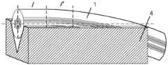
图2为应用本发明的光子晶体光纤及抛磨示意图;Fig. 2 is the photonic crystal fiber of the present invention and a schematic diagram of polishing;
图3(a)为应用本发明的两根光子晶体光纤的抛磨面贴合示意图;Fig. 3 (a) is the bonding schematic diagram of the polishing surface of two photonic crystal fibers of the present invention;
图3(b)为抛光面贴合后形成的Y型光纤示意图;Figure 3(b) is a schematic diagram of a Y-shaped optical fiber formed after bonding the polished surfaces;
图4为应用本发明制作的1×2光子晶体光纤耦合器示意图;4 is a schematic diagram of a 1 × 2 photonic crystal fiber coupler made by applying the present invention;
图5为应用本发明制作的2×2光子晶体光纤耦合器示意图;5 is a schematic diagram of a 2×2 photonic crystal fiber coupler made by applying the present invention;
图6(a)为应用本发明的空芯光子晶体光纤抛磨前的端面及研磨深度示意图;Figure 6 (a) is a schematic diagram of the end face and the grinding depth of the hollow-core photonic crystal fiber before being polished;
图6(b)为应用本发明的空芯光子晶体光纤抛磨面贴合后的端面示意图;Fig. 6 (b) is the schematic diagram of the end face of the hollow-core photonic crystal optical fiber after the polishing surface is bonded according to the present invention;
图7(a)为应用本发明的一种保偏光子晶体光纤抛磨前的端面及研磨深度示意图;Fig. 7 (a) is a schematic diagram of the end face and the grinding depth of a polarization-maintaining photonic crystal fiber before polishing;
图7(b)为应用本发明的保偏光子晶体光纤抛磨面贴合后的端面示意图;Figure 7(b) is a schematic view of the end face of the polarization-maintaining photonic crystal optical fiber after the polishing surface is bonded according to the present invention;
图8为不经过切割光纤直接产生的2×2光子晶体光纤耦合器示意图。Fig. 8 is a schematic diagram of a 2×2 photonic crystal fiber coupler directly generated without cutting the fiber.
附图符号说明:Explanation of reference symbols:
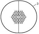
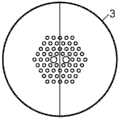
1、1′:光子晶体光纤,2、2′:光子晶体光纤抛磨面,3:Y分支光子晶体光纤顶点及端面,4、4′:抛磨基块,5、5′:Y分支光子晶体光纤,6:与Y分支光子晶体光纤连接的单根光纤,7:光纤连接区。1, 1': photonic crystal fiber, 2, 2': polished surface of photonic crystal fiber, 3: apex and end face of Y branch photonic crystal fiber, 4, 4': polished base block, 5, 5': Y branch photon Crystal fiber, 6: single fiber connected with Y branch photonic crystal fiber, 7: fiber connection area.
具体实施方式Detailed ways
为更清楚地说明本发明,下面将结合附图和实例对本发明做进一步的详细说明。In order to illustrate the present invention more clearly, the present invention will be further described in detail below in conjunction with the accompanying drawings and examples.
本发明提供了一种新型光子晶体光纤耦合器设计方法。其关键是Y分支光子晶体光纤5的制作,首先,分别研磨两根相同的光子晶体光纤1、1′,研磨至光纤中心处并对研磨面抛光;然后将两光子晶体光纤的抛光面2、2′采用光胶工艺贴合;对贴合后的光纤切端面处理得到端面平整的Y分支光子晶体光纤5。取Y分支光子晶体光纤顶点3与单根光子晶体光纤6或与另一个Y分支光子晶体光纤5′顶点进行熔接(对接),可分别得到分光比为50/50的1×2光子晶体光纤耦合器和2×2光子晶体光纤耦合器。The invention provides a novel photonic crystal fiber coupler design method. Its key is the making of Y branch photonic crystal fiber 5, at first, grind two identical
以Thorlabs公司的ESM-12-01无截止单模光子晶体光纤为实施例进行说明。首先对光纤研磨方向进行定位。将光子晶体光纤在研磨基块上舒展放置,即光纤不发生扭转。用显微镜观测其端面放置方向是否符合预定要求并进行相应微调,直到满足所需的研磨方向。定位后将光纤固定并开始打磨,可以采用光纤固定凹槽一端为水平方向的研磨基块或者基块组合来保证平坦段的切割精度。光子晶体光纤的研磨面结构参照图2所示,研磨面分为平坦段和过渡段,根据一般经验过渡段长度l′至少大于4cm。过渡段长度则关系到贴合后光纤的张角,并进一步影响耦合器插入损耗,研磨区过渡段的长度影响光纤张角,二者关系近似为:The ESM-12-01 uncut single-mode photonic crystal fiber of Thorlabs is taken as an example for illustration. Firstly, locate the fiber polishing direction. The photonic crystal fiber is stretched on the grinding base block, that is, the fiber does not twist. Use a microscope to observe whether the placement direction of the end face meets the predetermined requirements and make corresponding fine-tuning until the required grinding direction is met. After positioning, fix the optical fiber and start grinding. You can use a grinding base block or a combination of base blocks with one end of the fiber fixing groove in the horizontal direction to ensure the cutting accuracy of the flat section. The structure of the polished surface of the photonic crystal fiber is shown in Figure 2. The polished surface is divided into a flat section and a transition section. According to general experience, the length l' of the transition section is at least greater than 4cm. The length of the transition section is related to the opening angle of the fiber after bonding, and further affects the insertion loss of the coupler. The length of the transition section in the grinding area affects the opening angle of the fiber. The relationship between the two is approximately:
其中,l′为光子晶体光纤光纤研磨区过渡段的长度,d为纤芯直径,α为光纤张角,D为包层直径。光束从Y分支光子晶体光纤顶点输入时,光束在平坦段纤芯内传播与单根光纤相同,进入过渡段纤芯时纤芯缓慢展宽,满足场的连续性条件,不会激发高阶模,仅是基模的宽度随着波导的变宽而不断变宽并按相应分光比进入两个分支光纤,理想情况下其插入损耗只有分支纤芯交叉的张角产生的辐射模损耗。光纤张角越大则耦合器插入损耗越大,一般光纤张角α<2°,这就要求光纤研磨机有较大的研磨范围并且过渡段光纤的弯曲半径足够大。Among them, l' is the length of the transition section of the optical fiber polishing zone of the photonic crystal fiber, d is the core diameter, α is the opening angle of the fiber, and D is the cladding diameter. When the light beam is input from the apex of the Y-branch photonic crystal fiber, the propagation of the light beam in the core of the flat section is the same as that of a single fiber. The width of the fundamental mode increases with the width of the waveguide and enters the two branch fibers according to the corresponding splitting ratio. Ideally, the insertion loss is only the radiation mode loss caused by the crossing angle of the branch cores. The larger the opening angle of the fiber is, the greater the insertion loss of the coupler is. Generally, the opening angle of the fiber is α<2°, which requires that the fiber polishing machine has a larger grinding range and the bending radius of the fiber in the transition section is large enough.
ESM-12-01型光子晶体光纤纤芯直径约为10μm,光纤研磨机的精度高于0.2μm,可以保证将光子晶体光纤研磨至中心即研磨掉一半的精度要求。研磨结束后,对研磨面进行抛光处理,以便进行下一步的光纤贴合;为保证光胶质量,抛光面光洁度高于4级。除此之外,光子晶体光纤研磨和抛光过程会有光纤碎屑或者研磨颗粒等堵塞侧面已经被打磨开的空气孔,会极大影响导光性能。抛磨光子晶体光纤时,为避免堵塞空气孔,对光纤端面空气孔施加气压保持空气孔清洁,抛磨完成时采用超声波清洗抛磨产生中的碎屑。The core diameter of ESM-12-01 photonic crystal fiber is about 10 μm, and the precision of the optical fiber polishing machine is higher than 0.2 μm, which can guarantee the accuracy requirement of grinding the photonic crystal fiber to the center, that is, grinding half of it. After the grinding is finished, the grinding surface is polished for the next step of fiber bonding; in order to ensure the quality of the optical glue, the finish of the polished surface is higher than
采用光胶法对抛光后的光子晶体光纤贴合。对抛光面用蘸有酒精和乙醚的混合液光胶擦布擦拭抛光面,再用干布擦拭抛光面、吸去表面附着的灰尘等,将两个抛光面对准并轻轻按压实现光胶。将得到的Y型光纤贴合处用光纤切割刀切端面,并与另外一根光纤或者另一个Y型光子晶体光纤顶点熔接/对接,便可得到相应分光比的1×2光子晶体光纤耦合器和2×2光子晶体光纤耦合器。光纤接续过程中可以在耦合器一端光纤中打光,在另一侧的两根光子晶体光纤端口监测光功率,来确定是否达到最低接续损耗。The polished photonic crystal fiber is bonded by photoglue method. For the polishing surface, wipe the polishing surface with a mixed liquid light glue cloth dipped in alcohol and ether, and then wipe the polishing surface with a dry cloth to absorb the dust attached to the surface, align the two polishing surfaces and press gently to achieve the light glue . Use a fiber cutter to cut the end face of the obtained Y-shaped optical fiber, and weld/butt it with another optical fiber or another Y-shaped photonic crystal fiber to obtain a 1×2 photonic crystal fiber coupler with a corresponding splitting ratio and 2×2 photonic crystal fiber couplers. During the process of optical fiber splicing, light can be illuminated in the optical fiber at one end of the coupler, and the optical power can be monitored at the two photonic crystal optical fiber ports on the other side to determine whether the minimum splicing loss is reached.
同样,对于空芯光子晶体光纤上述制备也是适用的,研磨前和贴合后的端面如图6所示。由于空芯光子晶体光纤结构更加复杂,所以在抛磨过程中要尤其小心防止光纤崩断;另外,空芯光子晶体光纤的熔接损耗相对其他光纤较大,实际应用中接续方式可依情况选择熔接或端面对接。Similarly, the above preparation is also applicable to the hollow-core photonic crystal fiber, and the end faces before grinding and after bonding are shown in FIG. 6 . Since the structure of the hollow-core photonic crystal fiber is more complex, special care must be taken to prevent the fiber from breaking during the polishing process; in addition, the splicing loss of the hollow-core photonic crystal fiber is larger than that of other fibers, and the splicing method in practical applications can be selected according to the situation. or end-to-end.
这种工艺也适用于保偏光子晶体光纤耦合器的制作。当对保偏光子晶体光纤进行上述操作时,对光纤研磨方向的定位须使贴合后的光纤保偏结构不受到影响。图7所示为一种保偏光子晶体光纤研磨及贴合过程的示意图。在垂直于保偏光子晶体光纤快轴的方向上打磨掉光纤的一个大空气孔,将抛磨后的两个光纤贴合,其端面保偏结构与原保偏光子晶体光纤相同。This process is also applicable to the fabrication of polarization-maintaining photonic crystal fiber couplers. When performing the above operations on the polarization-maintaining photonic crystal fiber, the orientation of the fiber polishing direction must be such that the polarization-maintaining structure of the bonded fiber is not affected. FIG. 7 is a schematic diagram of a polarization-maintaining photonic crystal fiber polishing and bonding process. A large air hole in the fiber is polished in a direction perpendicular to the fast axis of the polarization-maintaining photonic crystal fiber, and the two polished fibers are bonded together, and the polarization-maintaining structure of the end face is the same as that of the original polarization-maintaining photonic crystal fiber.
在上述制备过程中,若采用常规研磨基块,光子晶体光纤抛磨区是常规的过渡段-平坦段-过渡段分布,当两个抛磨面贴合后,其本身就是一个2×2光子晶体光纤耦合器,如图8所示。In the above preparation process, if the conventional polishing base is used, the photonic crystal fiber polishing area is a conventional transition section-flat section-transition section distribution. When the two polishing surfaces are bonded together, it itself is a 2×2 photon Crystal fiber coupler, as shown in Figure 8.
Y分支光子晶体光纤的分光比可通过改变两个光纤抛磨区过渡段长度来设定分光比,当两抛磨面的过渡段长度相同时,理想贴合情况下分光比为50:50;另外,贴合两光纤抛磨面时,通过调节抛磨面间的轴向位移或错位也可以调节输出分光比,该过程可通过在Y分支光纤顶点处打光同时在两个分支的输出端记录光功率来监测实现。从这一点上看,通过调节研磨区弯曲半径和抛磨面的轴向对准位置可以实现其他分光比的光子晶体光纤耦合器的制作。The splitting ratio of the Y-branch photonic crystal fiber can be set by changing the length of the transition section of the two optical fiber polishing areas. When the length of the transition section of the two polishing surfaces is the same, the splitting ratio is 50:50 under ideal fit; In addition, when the two optical fiber polishing surfaces are attached, the output splitting ratio can also be adjusted by adjusting the axial displacement or misalignment between the polishing surfaces. Record optical power to monitor implementation. From this point of view, by adjusting the bending radius of the grinding area and the axial alignment position of the polishing surface, the fabrication of photonic crystal fiber couplers with other splitting ratios can be realized.
尽管上面对本发明说明性的具体实施方式进行了描述,以便于本技术领的技术人员理解本发明,但应该清楚,本发明不限于具体实施方式的范围,实施方式中的参数及附图仅是说明实施方式的示意图,并非对本发明形成限制。对本技术领域的普通技术人员来讲,只要各种变化在所附的权利要求限定和确定的本发明的精神和范围内,这些变化是显而易见的,一切利用本发明构思的发明创造均在保护之列。本发明未详细阐述的技术内容属于本领域技术人员的公知技术。Although the illustrative specific implementation of the present invention has been described above, so that those skilled in the art can understand the present invention, it should be clear that the present invention is not limited to the scope of the specific implementation, and the parameters and accompanying drawings in the implementation are only The schematic diagrams illustrate the embodiments, but do not limit the present invention. For those of ordinary skill in the art, as long as various changes are within the spirit and scope of the present invention defined and determined by the appended claims, these changes are obvious, and all inventions and creations utilizing the concept of the present invention are protected. List. The technical content not elaborated in the present invention belongs to the well-known technology of those skilled in the art.
Claims (9)
Priority Applications (1)
| Application Number | Priority Date | Filing Date | Title |
|---|---|---|---|
| CN201310482796.4ACN103499855B (en) | 2013-10-15 | 2013-10-15 | Photonic crystal optical fiber coupler and manufacturing method thereof |
Applications Claiming Priority (1)
| Application Number | Priority Date | Filing Date | Title |
|---|---|---|---|
| CN201310482796.4ACN103499855B (en) | 2013-10-15 | 2013-10-15 | Photonic crystal optical fiber coupler and manufacturing method thereof |
Publications (2)
| Publication Number | Publication Date |
|---|---|
| CN103499855Atrue CN103499855A (en) | 2014-01-08 |
| CN103499855B CN103499855B (en) | 2015-06-10 |
Family
ID=49865078
Family Applications (1)
| Application Number | Title | Priority Date | Filing Date |
|---|---|---|---|
| CN201310482796.4AExpired - Fee RelatedCN103499855B (en) | 2013-10-15 | 2013-10-15 | Photonic crystal optical fiber coupler and manufacturing method thereof |
Country Status (1)
| Country | Link |
|---|---|
| CN (1) | CN103499855B (en) |
Cited By (7)
| Publication number | Priority date | Publication date | Assignee | Title |
|---|---|---|---|---|
| CN107632345A (en)* | 2017-08-23 | 2018-01-26 | 中北大学 | Optical fiber macrobend coupled structure and its processing method based on uv-curable glue |
| CN108152889A (en)* | 2018-03-19 | 2018-06-12 | 江苏斯德雷特通光光纤有限公司 | It is a kind of to be used to make the device and method that high-precision low loss fiber Y divides device |
| CN108549128A (en)* | 2018-05-15 | 2018-09-18 | 复旦大学 | Hollow antiresonance photonic crystal optical fiber coupler and its application |
| WO2018205762A1 (en)* | 2017-05-12 | 2018-11-15 | 深圳市太赫兹科技创新研究院 | Terahertz beam splitter |
| CN110906919A (en)* | 2019-11-01 | 2020-03-24 | 北京航天时代光电科技有限公司 | High-performance hybrid optical fiber resonant cavity suitable for working in variable temperature environment |
| CN111897047A (en)* | 2020-06-19 | 2020-11-06 | 中国船舶重工集团公司第七0七研究所 | All-photonic crystal fiber polarizer based on fused biconical taper and manufacturing method thereof |
| CN115437065A (en)* | 2022-09-14 | 2022-12-06 | 深圳朗光科技有限公司 | Preparation method of optical fiber coupler and optical fiber coupler |
Citations (3)
| Publication number | Priority date | Publication date | Assignee | Title |
|---|---|---|---|---|
| JPH02242204A (en)* | 1989-03-16 | 1990-09-26 | Fujitsu Ltd | Optical fiber coupler |
| JP2012027402A (en)* | 2010-07-27 | 2012-02-09 | Nippon Telegr & Teleph Corp <Ntt> | Method for manufacturing directional coupler using optical fiber |
| CN103076653A (en)* | 2013-01-11 | 2013-05-01 | 暨南大学 | Production method of photonic crystal fiber coupler |
- 2013
- 2013-10-15CNCN201310482796.4Apatent/CN103499855B/ennot_activeExpired - Fee Related
Patent Citations (3)
| Publication number | Priority date | Publication date | Assignee | Title |
|---|---|---|---|---|
| JPH02242204A (en)* | 1989-03-16 | 1990-09-26 | Fujitsu Ltd | Optical fiber coupler |
| JP2012027402A (en)* | 2010-07-27 | 2012-02-09 | Nippon Telegr & Teleph Corp <Ntt> | Method for manufacturing directional coupler using optical fiber |
| CN103076653A (en)* | 2013-01-11 | 2013-05-01 | 暨南大学 | Production method of photonic crystal fiber coupler |
Non-Patent Citations (1)
| Title |
|---|
| 林锦海,等: "光纤耦合器的理论、设计及进展", 《物理学进展》* |
Cited By (10)
| Publication number | Priority date | Publication date | Assignee | Title |
|---|---|---|---|---|
| WO2018205762A1 (en)* | 2017-05-12 | 2018-11-15 | 深圳市太赫兹科技创新研究院 | Terahertz beam splitter |
| CN107632345A (en)* | 2017-08-23 | 2018-01-26 | 中北大学 | Optical fiber macrobend coupled structure and its processing method based on uv-curable glue |
| CN107632345B (en)* | 2017-08-23 | 2020-09-04 | 中北大学 | Optical fiber macrobend coupling structure based on UV curing adhesive and its processing method |
| CN108152889A (en)* | 2018-03-19 | 2018-06-12 | 江苏斯德雷特通光光纤有限公司 | It is a kind of to be used to make the device and method that high-precision low loss fiber Y divides device |
| CN108152889B (en)* | 2018-03-19 | 2023-07-14 | 江苏斯德雷特光纤科技有限公司 | Device and method for manufacturing high-precision low-loss optical fiber Y-splitter |
| CN108549128A (en)* | 2018-05-15 | 2018-09-18 | 复旦大学 | Hollow antiresonance photonic crystal optical fiber coupler and its application |
| CN110906919A (en)* | 2019-11-01 | 2020-03-24 | 北京航天时代光电科技有限公司 | High-performance hybrid optical fiber resonant cavity suitable for working in variable temperature environment |
| CN111897047A (en)* | 2020-06-19 | 2020-11-06 | 中国船舶重工集团公司第七0七研究所 | All-photonic crystal fiber polarizer based on fused biconical taper and manufacturing method thereof |
| CN111897047B (en)* | 2020-06-19 | 2022-07-26 | 中国船舶重工集团公司第七0七研究所 | All-photonic crystal fiber polarizer based on fused biconical taper and manufacturing method thereof |
| CN115437065A (en)* | 2022-09-14 | 2022-12-06 | 深圳朗光科技有限公司 | Preparation method of optical fiber coupler and optical fiber coupler |
Also Published As
| Publication number | Publication date |
|---|---|
| CN103499855B (en) | 2015-06-10 |
Similar Documents
| Publication | Publication Date | Title |
|---|---|---|
| CN103499855B (en) | Photonic crystal optical fiber coupler and manufacturing method thereof | |
| CN103728696B (en) | A kind of 1 �� N fiber coupler | |
| US4083625A (en) | Optical fiber junction device | |
| JP5307558B2 (en) | Multi-core photonic bandgap fiber with inter-core coupling | |
| CA1272896A (en) | Fiber-lens optical coupler | |
| CN101852894B (en) | Coupling method for suspended-core optical fibers | |
| CN102169209A (en) | Method for low loss welding and end face treatment of photonic crystal optical fiber | |
| CN111061011A (en) | Improved single-mode fiber and multi-core fiber coupler and preparation method thereof | |
| CN111830633A (en) | A coaxial dual waveguide fiber fan-in connector | |
| CN110542949B (en) | Optical fiber manufacturing method and heating device for silicon optical waveguide connection and coupling | |
| CN115407456B (en) | A double-layer polarization-independent grating coupler | |
| JP4129903B2 (en) | Method for manufacturing fused mode division directional coupler | |
| CN115805359B (en) | Laser processing system and processing method thereof | |
| US20210181422A1 (en) | Whispering gallery mode resonator and manufacturing method thereof | |
| CN106291821A (en) | A kind of hollow-core photonic crystal fiber bonder | |
| CN103698841B (en) | A kind of microstructure fiber device | |
| CN115576054A (en) | Mode spot converter based on integration of graded-index waveguide and two-dimensional inverted tapered waveguide | |
| CN203480073U (en) | Fiber combiner | |
| JP4417286B2 (en) | Holey fiber and fiber optic modules | |
| CN105785523B (en) | A kind of pump signal coupler and its process | |
| TWI279601B (en) | Making method of laser-polished fiber devices | |
| CN211348701U (en) | Polarization maintaining optical fiber array with high coupling rate | |
| JP7400152B2 (en) | Optical fiber connection body and connection structure between the optical fiber connection body and optical device | |
| JP5858838B2 (en) | Optical device manufacturing method | |
| CN110286442B (en) | An optical fiber coupler with adjustable coupling ratio |
Legal Events
| Date | Code | Title | Description |
|---|---|---|---|
| C06 | Publication | ||
| PB01 | Publication | ||
| C10 | Entry into substantive examination | ||
| SE01 | Entry into force of request for substantive examination | ||
| C14 | Grant of patent or utility model | ||
| GR01 | Patent grant | ||
| CF01 | Termination of patent right due to non-payment of annual fee | Granted publication date:20150610 |