CN103493378A - Data processing system - Google Patents
Data processing systemDownload PDFInfo
- Publication number
- CN103493378A CN103493378ACN201280019587.XACN201280019587ACN103493378ACN 103493378 ACN103493378 ACN 103493378ACN 201280019587 ACN201280019587 ACN 201280019587ACN 103493378 ACN103493378 ACN 103493378A
- Authority
- CN
- China
- Prior art keywords
- range
- data
- circuit
- voltage
- amplifier
- Prior art date
- Legal status (The legal status is an assumption and is not a legal conclusion. Google has not performed a legal analysis and makes no representation as to the accuracy of the status listed.)
- Granted
Links
Images


Classifications
- H—ELECTRICITY
- H03—ELECTRONIC CIRCUITRY
- H03M—CODING; DECODING; CODE CONVERSION IN GENERAL
- H03M1/00—Analogue/digital conversion; Digital/analogue conversion
- H03M1/12—Analogue/digital converters
- H03M1/18—Automatic control for modifying the range of signals the converter can handle, e.g. gain ranging
- H03M1/181—Automatic control for modifying the range of signals the converter can handle, e.g. gain ranging in feedback mode, i.e. by determining the range to be selected from one or more previous digital output values
- H03M1/183—Automatic control for modifying the range of signals the converter can handle, e.g. gain ranging in feedback mode, i.e. by determining the range to be selected from one or more previous digital output values the feedback signal controlling the gain of an amplifier or attenuator preceding the analogue/digital converter
- H—ELECTRICITY
- H03—ELECTRONIC CIRCUITRY
- H03M—CODING; DECODING; CODE CONVERSION IN GENERAL
- H03M1/00—Analogue/digital conversion; Digital/analogue conversion
- H03M1/12—Analogue/digital converters
- H03M1/124—Sampling or signal conditioning arrangements specially adapted for A/D converters
- H—ELECTRICITY
- H03—ELECTRONIC CIRCUITRY
- H03M—CODING; DECODING; CODE CONVERSION IN GENERAL
- H03M1/00—Analogue/digital conversion; Digital/analogue conversion
- H03M1/12—Analogue/digital converters
- H03M1/18—Automatic control for modifying the range of signals the converter can handle, e.g. gain ranging
- H03M1/181—Automatic control for modifying the range of signals the converter can handle, e.g. gain ranging in feedback mode, i.e. by determining the range to be selected from one or more previous digital output values
- H03M1/182—Automatic control for modifying the range of signals the converter can handle, e.g. gain ranging in feedback mode, i.e. by determining the range to be selected from one or more previous digital output values the feedback signal controlling the reference levels of the analogue/digital converter
- H—ELECTRICITY
- H03—ELECTRONIC CIRCUITRY
- H03M—CODING; DECODING; CODE CONVERSION IN GENERAL
- H03M1/00—Analogue/digital conversion; Digital/analogue conversion
- H03M1/12—Analogue/digital converters
- H03M1/20—Increasing resolution using an n bit system to obtain n + m bits
Landscapes
- Engineering & Computer Science (AREA)
- Theoretical Computer Science (AREA)
- Analogue/Digital Conversion (AREA)
Abstract
Description
Translated fromChinese技术领域technical field
本发明涉及具有AD(Analog to Digital)转换功能的数据处理系统,尤其涉及用于得到比AD转换电路的位精度更高的位精度(分辨率)的技术。The present invention relates to a data processing system having an AD (Analog to Digital) conversion function, and in particular to a technique for obtaining higher bit precision (resolution) than that of an AD conversion circuit.
背景技术Background technique
在专利文献1中记载有如下技术:施加振幅与AD转换电路的最小分辨率大致相等的斜坡电压,进行多次AD转换动作,并通过具有比AD转换电路的位数更大位数的运算电路将各数字输出平均化,由此实现高精度AD转换。
在专利文献2中,通过差动放大器获取输入模拟信号和与转换量程相应的基准信号的差分,通过AD转换电路将其转换成数字信号,并通过接收该数字信号的控制装置根据与该差分相应的数字信号来控制基准信号且根据数字信号和转换量程来生成输出数字信号。与实际的AD转换电路的分辨率相比能够得到数倍转换量程的分辨率,并通过转换量程的设定方式得到需要的分辨率。In
现有技术文献prior art literature
专利文献patent documents
专利文献1:日本特开平5-14201号公报Patent Document 1: Japanese Patent Application Laid-Open No. 5-14201
专利文献2:日本特开平6-334523号公报Patent Document 2: Japanese Patent Application Laid-Open No. 6-334523
发明内容Contents of the invention
本发明人就在AD转换电路的转换量程的整个区域内提高其分辨率进行了研究。在专利文献1中难以实现该目的。在专利文献2中,在AD转换电路中将转换量程的基准信号与被测定用的输入信号的差分放大,由此提高转换位精度,但考虑到为了根据被测定信号对转换量程进行最适切换,必须对AD转换结果是否脱离转换量程进行判断来进行基准信号的切换,从而导致针对转换量程的切换的跟踪性较差,另外,也没有研究切换转换量程时的转换量程间的转换数据的连续性,而且,也没有明示差动放大电路的放大率与被放大的分辨率的关系,从而认为还需要进行各种其他研究。The inventors of the present invention conducted research on improving the resolution of an AD conversion circuit over the entire range of its conversion range. In
本发明的目的在于提供一种数据处理系统,能够在AD转换电路的转换量程的整个区域内提高其分辨率,并且对转换量程的切换的跟踪性良好,且其转换误差小。An object of the present invention is to provide a data processing system capable of improving the resolution of an AD conversion circuit over the entire range of the conversion range, having good followability to switching of the conversion range, and having a small conversion error.
本发明的上述目的以及其他目的和新型特征可以根据本说明书的记载和添加的附图得以明确。The above object and other objects and novel features of the present invention will be clarified from the description of this specification and the attached drawings.
简单说明本申请所公开的发明中具有代表性方案的概要,如下所述。Outlines of representative aspects among the inventions disclosed in the present application will be briefly described as follows.
即,相对于AD转换电路的分辨率得到将位精度扩展n(n为正整数)位的AD转换结果的数据处理系统,将AD转换电路的输入量程分割成m(2n≤m)部分,运算使各分割量程的连接点的电压在相邻的分割量程中彼此相同的数字偏移,对被测定模拟信号判断基于AD转换电路而得到的AD转换结果属于哪一分割量程,将使判断出的分割量程的范围成为AD转换电路的输入量程的电压范围的放大器偏移提供给可编程增益放大器而放大,将放大后的信号在AD转换电路中进行转换,对其转换结果进行低位侧的n位扩展并对扩展后的值进行基于上述可编程增益放大器的实测增益的除法运算,使其结果与对应的分割量程的数字偏移相加而得到将位精度扩展n位的AD转换结果。That is, with respect to the resolution of the AD conversion circuit, the data processing system that obtains the AD conversion result of expanding the bit precision by n (n is a positive integer) bits divides the input range of the AD conversion circuit into m (2n ≤ m) parts, Calculate the digital offset that makes the voltage of the connection point of each divided range the same in adjacent divided ranges, and judge which divided range the AD conversion result obtained based on the AD conversion circuit belongs to for the analog signal to be measured. The range of the divided range becomes the voltage range of the input range of the AD conversion circuit. The amplifier offset is provided to the programmable gain amplifier for amplification, and the amplified signal is converted in the AD conversion circuit, and the conversion result is converted to the low side n Bit extension and division operation based on the measured gain of the programmable gain amplifier for the extended value, adding the result to the digital offset of the corresponding divided range to obtain an AD conversion result with bit precision extended by n bits.
发明效果Invention effect
简单说明根据本申请所公开的发明中具有代表性的方案而得到的效果,如下所述。Effects obtained by typical aspects of the inventions disclosed in this application will be briefly described as follows.
即,能够在AD转换电路的转换量程的整个区域内提高其分辨率,并且对转换量程的切换的跟踪性良好且能够减小其转换误差。That is, the resolution of the AD conversion circuit can be improved over the entire range of the conversion range, and the switching error of the conversion range can be reduced with good followability.
附图说明Description of drawings
图1是例示本发明的第1实施方式的数据处理系统的框图。FIG. 1 is a block diagram illustrating a data processing system according to a first embodiment of the present invention.
图2是整体地例示本实施方式的AD转换原理的动作说明图。FIG. 2 is an operation explanatory diagram generally illustrating the principle of AD conversion in this embodiment.
图3是表示放大器偏移的设定例的说明图。FIG. 3 is an explanatory diagram showing a setting example of an amplifier offset.
图4是着眼于分割量程的区间2而示出本实施方式的上述AD转换原理的说明图。FIG. 4 is an explanatory diagram showing the above-mentioned AD conversion principle of the present embodiment focusing on the
图5是着眼于分割量程的区间3而示出本实施方式的上述AD转换原理的说明图。FIG. 5 is an explanatory diagram showing the above-mentioned AD conversion principle of the present embodiment focusing on the section 3 of the divided range.
图6是同样地着眼于分割量程的区间3而示出本实施方式的上述AD转换原理并且示出在可编程增益放大器保持放大动作的直线性的电压范围内使区间交错的情况的说明图。FIG. 6 is an explanatory diagram showing the above-mentioned AD conversion principle of the present embodiment focusing on the section 3 of the divided range, and showing a case where the sections are interleaved in the voltage range in which the programmable gain amplifier maintains the linearity of the amplification operation.
图7是同样地着眼于分割量程的区间2而示出本实施方式的上述AD转换原理并且示出在可编程增益放大器保持放大动作的直线性的电压范围内使区间交错的情况的说明图。FIG. 7 is an explanatory diagram showing the above-mentioned AD conversion principle of the present embodiment focusing on the
图8是整体地例示基于本实施方式的AD转换原理而进行的转换处理程序的流程图。FIG. 8 is a flowchart generally illustrating a conversion processing program based on the AD conversion principle of this embodiment.
图9是例示数字偏移数据DFS2的生成处理的流程图。FIG. 9 is a flowchart illustrating generation processing of digital offset data DFS2.
图10是例示已知的数字偏移数据DFS2的高位侧数字偏移数据DFS3的生成处理的流程图。FIG. 10 is a flowchart illustrating a generation process of the upper-order side digital offset data DFS3 of the known digital offset data DFS2.
图11是例示已知的数字偏移数据DFS2的低位侧数字偏移数据DFS1的生成处理的流程图。FIG. 11 is a flowchart illustrating generation processing of the lower-order-side digital offset data DFS1 of the known digital offset data DFS2.
图12是例示输入区间的判断处理RT3及上述AD转换处理RT4的详细情况的流程图。FIG. 12 is a flowchart illustrating details of the input section determination process RT3 and the AD conversion process RT4 described above.
图13是例示增益修正及数字偏移相加处理RT5的详细情况的流程图。FIG. 13 is a flowchart illustrating details of the gain correction and digital offset addition process RT5.
图14是例示本实施方式的AD转换动作的时序图。FIG. 14 is a timing chart illustrating an AD conversion operation in this embodiment.
图15是例示本发明的第2实施方式的数据处理系统的框图。FIG. 15 is a block diagram illustrating a data processing system according to a second embodiment of the present invention.
图16是例示被测定模拟信号的采样保持动作的动作说明图。FIG. 16 is an operation explanatory diagram illustrating an example of a sample-and-hold operation of an analog signal to be measured.
图17是例示使采样保持电路201保持的信息通过PGA102而在ADC113中进行AD转换的动作的动作说明图。FIG. 17 is an operation explanatory diagram illustrating an operation of performing AD conversion in the
图18是例示增益修正及数字偏移相加处理RT5中的动作的动作说明图。FIG. 18 is an operation explanatory diagram illustrating an operation in the gain correction and digital offset addition processing RT5.
图19是例示在被测定模拟信号的中央值接近AD转换电路的输入量程的中央值时将上述AD转换电路的输入量程的分割数设定成偶数而进行AD转换处理的情况的动作说明图。19 is an operation explanatory diagram exemplifying a case where AD conversion processing is performed by setting the number of divisions of the input range of the AD conversion circuit to an even number when the median value of the analog signal to be measured is close to the median value of the input range of the AD conversion circuit.
图20是以在被测定模拟信号的中央值接近AD转换电路的输入量程的中央值时将上述AD转换电路的输入量程的分割数设定成奇数例如分割成五部分而进行AD转换处理的方式进行控制时的第3实施方式的说明图。FIG. 20 is a method in which the number of divisions of the input range of the AD conversion circuit is set to an odd number, for example, divided into five parts to perform AD conversion processing when the median value of the analog signal to be measured is close to the median value of the input range of the AD conversion circuit. An explanatory diagram of the third embodiment at the time of control.
图21是例示第4实施方式的数据处理系统的框图。FIG. 21 is a block diagram illustrating a data processing system according to a fourth embodiment.
图22是例示DA转换电路集成为一个的情况下的针对PGA的增益校正的概要的说明图。FIG. 22 is an explanatory diagram illustrating an overview of gain correction for the PGA when DA conversion circuits are integrated into one.
图23是例示图22的处理RT10和RT11的详细情况的动作说明图。FIG. 23 is an operation explanatory diagram illustrating details of processes RT10 and RT11 in FIG. 22 .
图24是例示处理RT12的详细情况的动作说明图。FIG. 24 is an operation explanatory diagram illustrating details of the processing RT12.
图25是例示处理RT13及RT14的详细情况的动作说明图。FIG. 25 is an operation explanatory diagram illustrating details of processing RT13 and RT14.
图26是例示处理RT15的详细情况的动作说明图。FIG. 26 is an operation explanatory diagram illustrating details of the processing RT15.
图27是例示计算区间3的数字偏移时的流程中的A及B部分的详细情况的动作说明图。FIG. 27 is an operation explanatory diagram illustrating the details of parts A and B in the flow for calculating the digital offset of section 3. FIG.
图28是例示计算区间3的数字偏移时的流程中的C部分的详细情况的动作说明图。FIG. 28 is an operation explanatory diagram illustrating the details of part C in the flow for calculating the digital offset of section 3. FIG.
具体实施方式Detailed ways
1.实施方式的概要1. Outline of Embodiment
首先,对本申请所公开的发明中具有代表性的实施方式说明概要。在对代表性的实施方式进行的概要说明中,标以括号而参照的附图中的附图标记只不过是例示其包含在标以括号的构成要素的概念中。First, an outline of typical embodiments among the inventions disclosed in this application will be described. In the summary description of the typical embodiments, the reference numerals in the drawings referred to in parentheses are merely examples of the concepts included in the components in parentheses.
〔1〕<按ADC的分割输入量程进行输入的放大、AD转换、位扩展>[1] <Input amplification, AD conversion, and bit expansion according to the divided input range of the ADC>
本发明的代表性实施方式的数据处理系统100、200、300为得到对AD转换电路的分辨率进行了n(n为正整数)位扩展的AD转换结果的系统,具有AD转换电路113、可编程增益放大器102、以及控制电路110、110A、110B。上述控制电路将上述AD转换电路的输入量程分割成m(2n≤m)部分,准备使各分割量程的连接点的电压在相邻的分割量程中彼此相同的数字偏移,对被测定模拟信号判断基于上述AD转换电路而得到的AD转换结果属于哪一分割量程,将使判断出的分割量程的电压范围成为上述AD转换电路的输入量程的电压范围的放大器偏移和增益的指定提供给上述可编程增益放大器而放大,将放大后的信号在上述AD转换电路中进行转换,对该转换结果进行n位扩展和基于上述可编程增益放大器的实测增益的值的除法运算,并和与此对应的分割量程的数字偏移相加而得到将位精度扩展n位的AD转换结果。The
由此,根据对AD转换电路的输入量程的分割数m,能够在满足2n≤m的关系的范围内最终得到将位精度扩展n位的AD转换结果。此时,由于将用于使判断出的分割量程的范围成为AD转换电路的输入量程的电压范围的放大器偏移和增益的指定提供给可编程增益放大器而进行放大,所以可编程增益放大器以增益2n或在其附近进行放大。此时,按AD转换电路的分割输入量程进行输入的放大、AD转换、以及n位扩展,由此能够对可编程增益放大器的增益误差进行修正。而且,提供分割量程的最小值的数字偏移和在其低位相邻的分割量程的最大值相同。因此,能够在AD转换电路的转换量程的整个区域内相对于高分辨率的AD转换结果实现转换误差小的高转换精度。而且,即使在选择转换量程时也不通过可编程增益放大器进行放大而只要在AD转换电路中进行一次AD转换来判断即可,因此,在切换转换量程时也能够得到良好的跟踪性。Accordingly, according to the division number m of the input range to the AD conversion circuit, it is possible to finally obtain an AD conversion result in which the bit precision is extended by n bits within a range satisfying the relationship of 2n ≤ m. At this time, since the designation of amplifier offset and gain for making the range of the determined divided range to be the voltage range of the input range of the AD conversion circuit is provided to the programmable gain amplifier for amplification, the programmable gain amplifier uses the
〔2〕<增益误差的获取>[2] <Acquisition of gain error>
在项1的数据处理系统中,从上述控制电路提供给上述可编程增益放大器的增益为目的增益2n,基于上述控制电路而进行的n位扩展是对AD转换结果的低位进行的0扩展。In the data processing system of
由此,能够容易地使可编程增益放大器的增益误差抵消。Thus, it is possible to easily cancel the gain error of the programmable gain amplifier.
〔3〕<实测增益的获取>[3] <Acquisition of measured gain>
在项2的数据处理系统中,上述控制电路对上述可编程增益放大器设定上述2n来作为目的增益,根据将基于设定后的可编程增益放大器而得到的模拟信号的放大输出在AD转换电路中转换后的数字值、与此时向可编程增益放大器供给的模拟信号的生成用的数字值之差而获取相对于目的增益的实测增益。In the data processing system of
由此,能够容易地获取用于使基于可编程增益放大器的放大误差抵消的可编程增益放大器的实测增益。Thereby, the measured gain of the programmable gain amplifier for canceling the amplification error by a programmable gain amplifier can be acquired easily.
〔4〕<使相邻的分割量程的边界部分交错>〔4〕<Staggering the boundaries of adjacent divided ranges>
在项1的数据处理系统中,上述控制电路以使相邻的分割量程的边界部分交错的方式设定上述放大器偏移。In the data processing system according to
由此,能够避免使用对按照可编程增益放大器的放大特性而难以保证线性度的最小及最大输入附近的输入的放大功能,在该方面能够有助于降低AD转换误差。Accordingly, it is possible to avoid using an amplification function for inputs near the minimum and maximum inputs where it is difficult to ensure linearity due to the amplification characteristics of the programmable gain amplifier, and this can contribute to reducing AD conversion errors.
〔5〕<所属的分割量程的判断>〔5〕<Judgement of the division range to which it belongs>
在项1的数据处理系统中,上述控制电路根据对上述AD转换电路的各分割量程的边界电压的输入电压的AD转换数据来判断被测定电压所属的输入量程。In the data processing system of
由此,能够容易地判断出被测定信号所属的分割量程。Accordingly, it is possible to easily determine the divided range to which the signal to be measured belongs.
〔6〕<采样保持>[6] <Sample and hold>
在项1的数据处理系统中,还具有输入被测定模拟信号的采样保持电路201,上述控制电路110A、110B使用被上述采样保持电路采样的相同的被测定模拟信号而进行分割量程的判断、和使判断出的分割量程的电压范围成为上述AD转换电路的输入量程的电压范围的AD转换。In the data processing system of
由此,由于能够对相同的被测定模拟信号进行分割量程的判断和利用了该判断结果的上述AD转换,所以能够将发生误用不同的分割量程而进行AD转换的事态防患于未然。As a result, determination of the divided range and AD conversion using the result of the determination can be performed on the same analog signal to be measured. Therefore, it is possible to prevent a situation in which AD conversion is performed by erroneously using a different divided range.
〔7〕<使输入量程的分割数为奇数>[7] <Make the number of divisions of the input range an odd number>
在项1的数据处理系统中,上述控制电路在被测定模拟信号的中央值接近AD转换电路的输入量程的中央值时将上述AD转换电路的输入量程的分割数设定成奇数而进行AD转换用的上述处理。In the data processing system of
由此,能够抑制被测定模拟信号的中央值处于分割量程的边界附近。若其处于分割量程的边界附近,则必须在每当被测定模拟信号越过该中央值而变化时进行改变分割量程的处理,AD转换处理效率降低。Accordingly, it is possible to suppress the median value of the analog signal to be measured from being near the boundary of the divided range. If it is near the boundary of the divided range, it is necessary to perform processing for changing the divided range every time the analog signal to be measured changes beyond the central value, and the AD conversion processing efficiency decreases.
〔8〕<使放大器偏移生成用和放大器输入信号生成用的DAC分体化>[8] <Separate the DAC for amplifier offset generation and amplifier input signal generation>
在项1的数据处理系统中,分别具有向上述可编程增益放大器输出上述放大器偏移的DA转换电路115、和选择性地向上述可编程增益放大器输出设定用模拟信号的DA转换电路114。The data processing system of
由此,由于能够并行地进行放大器偏移的设定和设定用模拟信号的生成,所以有助于提高获取数字偏移时的处理效率。As a result, setting of the amplifier offset and generation of the setting analog signal can be performed in parallel, which contributes to improvement in processing efficiency when acquiring the digital offset.
〔9〕<使放大器偏移生成用和放大器输入信号生成用的DAC共用化>[9] <Common use of DAC for amplifier offset generation and amplifier input signal generation>
在项1的数据处理系统中,具有:选择性地取代上述被测定模拟信号而对设定用模拟信号进行采样保持并将其输出到上述可编程增益放大器的采样保持电路201;兼用于放大器偏移的生成和设定用模拟信号的生成的DA转换电路(图21的114);和对将在上述DA转换电路中生成的放大器偏移向上述可编程增益放大器输出的路径或将在上述DA转换电路中生成的设定用模拟信号向上述采样保持电路供给的路径进行选择的选择电路220。In the data processing system of
由此,必须串行地进行放大器偏移的设定和设定用模拟信号的生成,但由于DA转换电路的兼用而能够有助于缩小电路规模。Therefore, setting of the amplifier offset and generation of an analog signal for setting must be performed serially, but the dual function of the DA conversion circuit can contribute to reduction in circuit scale.
〔10〕<按ADC的分割输入量程进行输入的放大、AD转换、位扩展、由实测增益进行除法运算>〔10〕<Input amplification, AD conversion, bit expansion, division by measured gain>
本发明的其他实施方式的数据处理系统100、200、300具有AD转换电路113、可编程增益放大器102、以及控制电路110、110A、110B。上述控制电路判断被测定模拟信号属于将上述AD转换电路的输入量程分割成m(正整数)部分后的哪一分割量程,对上述可编程增益放大器设定用于将判断出的分割量程的电压范围放大至上述AD转换电路的输入量程的电压范围的放大器偏移和目的增益2n(n为正整数,2n≤m),将基于设定后的可编程增益放大器而得到的上述被测定模拟信号的放大信号在上述AD转换电路中进行转换,对转换后的数据进行n位的位扩展并对扩展后的数据进行基于上述可编程增益放大器的实测增益的除法运算,并使除法运算结果和与该分割量程对应的分割量程的数字偏移数据相加,从而获取将位精度扩展n位的AD转换结果。
由此,根据对AD转换电路的输入量程的分割数m,能够在满足2n≤m的关系的范围内最终得到将位精度扩展n位的AD转换结果。此时,由于将用于使判断出的分割量程的范围成为AD转换电路的输入量程的电压范围的放大器偏移和增益的指定提供给可编程增益放大器而进行放大,所以可编程增益放大器以增益2n或其附近进行放大。此时,按AD转换电路的分割输入量程进行输入的放大、AD转换、n位扩展、以及基于可编程增益放大器的实测增益的除法运算,由此能够对可编程增益放大器的增益误差进行修正。因此,能够在AD转换电路的转换量程的整个区域内使可编程增益放大器的增益误差抵消且得到将位精度扩展n位的AD转换结果。而且,即使在选择转换量程时也不通过可编程增益放大器进行放大而只要在AD转换电路中进行一次AD转换来判断即可,因此,在切换转换量程时也能够得到良好的跟踪性。Accordingly, according to the division number m of the input range to the AD conversion circuit, it is possible to finally obtain an AD conversion result in which the bit precision is extended by n bits within a range satisfying the relationship of 2n ≤ m. At this time, since the designation of amplifier offset and gain for making the range of the determined divided range to be the voltage range of the input range of the AD conversion circuit is provided to the programmable gain amplifier for amplification, the programmable gain amplifier uses the
〔11〕<作为基准的区间的数字偏移数据的生成>[11] <Creation of digital offset data for a reference section>
项10的数据处理系统具有第1DA转换电路114及第2DA转换电路115,上述控制电路进行第1处理至第5处理的控制。第1处理为如下处理,在上述第1DA转换电路中生成特定的上述分割量程的任意电压,将其在上述AD转换电路中进行转换而得到第1数据。第2处理为如下处理,在上述第1数据的低位侧根据该分割量程进行n位的位扩展而得到第2数据。第3处理为如下处理,在上述第1DA转换电路中生成上述特定的分割量程的任意电压,并且在上述第2DA转换电路中生成用于将该分割量程的电压范围放大至上述AD转换电路的输入量程的电压范围的放大器偏移,通过设定有所生成的放大器偏移和目的增益2n的上述可编程增益放大器将在上述第1DA转换电路中生成的任意电压放大,并将放大后的信号在上述AD转换电路中进行转换而得到第3数据。第4处理为如下处理,将上述第3数据在低位侧扩展n位并使扩展后的数据由上述实测增益进行除法运算而得到第4数据。第5处理为如下处理,从上述第2数据减去第4数据而得到该特定的分割量程的数字偏移数据。The data processing system of
由此,在特定的上述分割量程的电压范围内,将对通过可编程增益放大器而放大的输入量程的电压范围进行AD转换后的结果扩展n位并由上述实测增益进行除法运算后的值和上述数字偏移数据相加,所得到的值与不经由可编程增益放大器而直接进行AD转换后的值实质一致。Thus, within the specified voltage range of the above-mentioned divided range, the result obtained by AD-converting the voltage range of the input range amplified by the programmable gain amplifier by n bits and divided by the above-mentioned actual measurement gain and The above-mentioned digital offset data is added, and the obtained value is substantially consistent with the value obtained by directly performing AD conversion without going through the programmable gain amplifier.
〔12〕<数字偏移数据已知区间的高位侧数字偏移数据的生成>[12] <Generation of high-order-side digital offset data in the digital offset data known section>
在项11的数据处理系统中,在生成上述特定的分割量程的数字偏移数据后,在生成该分割量程的高位侧的分割量程的数字偏移数据时,上述控制电路进行第6处理至第9处理。第6处理为如下处理,在上述第1DA转换电路中生成上述特定的分割量程的最大电压,并且在上述第2DA转换电路中生成用于将该分割量程的电压范围放大至上述AD转换电路的输入量程的电压范围的放大器偏移,通过设定有所生成的放大器偏移和目的增益2n的上述可编程增益放大器将在上述第1DA转换电路中生成的最大电压放大,并将放大后的信号在上述AD转换电路中进行转换而得到第6数据。第7处理为如下处理,将上述第6数据在低位侧扩展n位并使扩展后的数据由上述实测增益进行除法运算,使该结果与上述特定的分割量程的数字偏移数据相加而得到第7数据。第8处理为如下处理,在上述第1DA转换电路中生成上述高位侧的分割量程的最小电压,并且在上述第2DA转换电路中生成用于将该分割量程的电压范围放大至上述AD转换电路的输入量程的电压范围的放大器偏移,通过设定有所生成的放大器偏移和目的增益2n的上述可编程增益放大器将在上述第1DA转换电路中生成的最小电压放大,并将放大后的信号在上述AD转换电路中进行转换而得到第8数据。第9处理为如下处理,将上述第8数据在低位侧扩展n位并使扩展后的数据由上述实测增益进行除法运算,从上述第7数据减去该结果而得到上述高位侧分割量程的数字偏移数据。In the data processing system of item 11, after generating the digital offset data of the above-mentioned specific divided range, when generating the digital offset data of the divided range on the upper side of the divided range, the control circuit performs the sixth processing to the first processing. 9 processing. The sixth process is a process of generating the maximum voltage of the specified divided range in the first DA conversion circuit, and generating an input for amplifying the voltage range of the divided range to the AD conversion circuit in the second DA conversion circuit. The amplifier offset of the voltage range of the measurement range, the maximum voltage generated in the above-mentioned first DA conversion circuit is amplified by setting the generated amplifier offset and the above-mentioned programmable gain amplifier of the target gain2n , and the amplified signal Conversion is carried out in the above-mentioned AD conversion circuit to obtain sixth data. The seventh process is the process of extending the sixth data by n bits on the lower order side, dividing the expanded data by the actual measurement gain, and adding the result to the digital offset data of the specified divided range. 7th data. The eighth process is a process of generating, in the first DA conversion circuit, the minimum voltage of the high-order-side divided range, and generating, in the second DA conversion circuit, a voltage range for amplifying the divided range to the AD conversion circuit. The amplifier offset of the voltage range of the input range, the minimum voltage generated in the above-mentioned first DA conversion circuit is amplified by setting the generated amplifier offset and the above-mentioned programmable gain amplifier of the target gain2n , and the amplified The signal is converted in the AD conversion circuit to obtain eighth data. The ninth process is the process of extending the above-mentioned eighth data by n bits on the low-order side, dividing the expanded data by the above-mentioned actual measurement gain, and subtracting the result from the above-mentioned seventh data to obtain the number of the above-mentioned high-order side divided range. Offset data.
由此,由于使用已知的数字偏移数据进行运算从而使求出已知的数字偏移数据的特定分割量程和与其相邻的高位侧分割量程的连接点的电压在双方的分割量程中一致,所以能够保证特定分割量程和与其相邻的高位侧分割量程的连续性。而且在该分割量程的电压范围内,将对通过可编程增益放大器而放大的输入量程的电压范围进行AD转换后的结果扩展n位并由上述实测增益进行除法运算后的值和上述数字偏移数据相加,所得到的值与不经由可编程增益放大器而直接进行AD转换后的值实质一致。尤其是,由于对在各个分割量程进行AD转换后的值进行n位的位扩展和对该结果由实测增益进行除法运算,所以能够排除可编程增益放大器的增益误差的影响,从而能够高精度地保证其连续性。Thus, since known digital offset data is used for calculation, the voltage at the connection point between the specific divided range for which the known digital offset data is obtained and the adjacent high-order side divided range is consistent in both divided ranges , so the continuity of a specific split range and its adjacent high-order side split range can be guaranteed. In addition, within the voltage range of the divided range, the result of AD conversion of the voltage range of the input range amplified by the programmable gain amplifier is extended by n bits, and the value obtained by dividing by the above-mentioned measured gain and the above-mentioned digital offset The data are added, and the obtained value is substantially the same as the value directly subjected to AD conversion without going through the programmable gain amplifier. In particular, since the value after AD conversion in each divided range is extended by n bits and the result is divided by the measured gain, the influence of the gain error of the programmable gain amplifier can be eliminated, thereby enabling high-precision ensure its continuity.
〔13〕<数字偏移数据已知区间的低位侧数字偏移数据的生成>[13] <Generation of digital offset data on the low-order side of the known digital offset data section>
在项11的数据处理系统中,在生成上述特定的分割量程的数字偏移数据后,在生成该分割量程的低位侧的分割量程的数字偏移数据时,上述控制电路进行第10处理至第13处理。第10处理为如下处理,在上述第1DA转换电路中生成上述特定的分割量程的最小电压,并且在上述第2DA转换电路中生成用于将该分割量程的电压范围放大至上述AD转换电路的输入量程的电压范围的放大器偏移,通过设定有所生成的放大器偏移和目的增益2n的上述可编程增益放大器将在上述第1DA转换电路中生成的最小电压放大,并将放大后的信号在上述AD转换电路中进行转换而得到第10数据。第11处理为如下处理,将上述第10数据在低位侧扩展n位并使扩展后的数据由上述实测增益进行除法运算,使该结果与特定的分割量程的数字偏移数据相加而得到第11数据。第12处理为如下处理,在上述第1DA转换电路中生成上述低位侧的分割量程的最大电压,并且在上述第2DA转换电路中生成用于将该分割量程的电压范围放大至上述AD转换电路的输入量程的电压范围的放大器偏移,通过设定有所生成的放大器偏移和目的增益2n的上述可编程增益放大器将在上述第1DA转换电路中生成的最大电压放大,并将放大后的信号在上述AD转换电路中进行转换而得到第12数据。第13处理为如下处理,将上述第12数据在低位侧扩展n位并使扩展后的数据由上述实测增益进行除法运算,从上述第11数据减去该结果而得到上述低位侧分割量程的数字偏移数据。In the data processing system of item 11, after generating the digital offset data of the specific divided range, when generating the digital offset data of the divided range on the lower side of the divided range, the control circuit performs the tenth process to the first step. 13 processing. The tenth process is a process of generating the minimum voltage of the specified divided range in the first DA conversion circuit, and generating an input for amplifying the voltage range of the divided range to the AD conversion circuit in the second DA conversion circuit. The amplifier offset of the voltage range of the measuring range, the minimum voltage generated in the above-mentioned first DA conversion circuit is amplified by setting the generated amplifier offset and the above-mentioned programmable gain amplifier of the target gain2n , and the amplified signal Conversion is performed in the AD conversion circuit described above to obtain the tenth data. The eleventh processing is the processing of extending the above-mentioned tenth data by n bits on the low-order side, dividing the extended data by the above-mentioned actual measurement gain, and adding the result to the digital offset data of a specific divided range to obtain the first 11 data. The twelfth process is a process of generating, in the first DA conversion circuit, the maximum voltage of the low-order side divided range, and generating, in the second DA conversion circuit, a voltage for amplifying the voltage range of the divided range to the AD conversion circuit. The amplifier offset of the voltage range of the input range, the maximum voltage generated in the above-mentioned first DA conversion circuit is amplified by setting the generated amplifier offset and the above-mentioned programmable gain amplifier of the target gain2n , and the amplified The signal is converted in the AD conversion circuit to obtain twelfth data. The thirteenth process is the process of extending the above-mentioned twelfth data by n bits on the low-order side, dividing the extended data by the above-mentioned actual measurement gain, and subtracting the result from the above-mentioned eleventh data to obtain the number of the above-mentioned low-order side divided range. Offset data.
由此,由于使用已知的基准数字偏移数据进行运算从而使求出已知的数字偏移数据的特定分割量程和与其相邻的低位侧分割量程的连接点的电压在双方的分割量程内一致,所以能够保证特定分割量程和与其相邻的低位侧分割量程的连续性。而且在该分割量程的电压范围内,将对通过可编程增益放大器而放大的输入量程的电压范围进行AD转换后的结果扩展n位并由上述实测增益进行除法运算后的值和上述数字偏移数据相加,所得到的值与不经由可编程增益放大器而直接进行AD转换后的值实质一致。尤其是,由于对在各个分割量程进行AD转换后的值进行n位的位扩展和对该结果由实测增益进行除法运算,所以能够排除可编程增益放大器的增益误差的影响,从而能够高精度地保证其连续性。As a result, since known reference digital offset data is used for calculation, the voltage at the connection point between the specific divided range for which the known digital offset data is obtained and its adjacent low-order divided range is within the divided ranges of both Consistent, so the continuity of a specific split range and its adjacent lower side split range can be guaranteed. In addition, within the voltage range of the divided range, the result of AD conversion of the voltage range of the input range amplified by the programmable gain amplifier is extended by n bits, and the value obtained by dividing by the above-mentioned measured gain and the above-mentioned digital offset The data are added, and the obtained value is substantially the same as the value directly subjected to AD conversion without going through the programmable gain amplifier. In particular, since the value after AD conversion in each divided range is extended by n bits and the result is divided by the measured gain, the influence of the gain error of the programmable gain amplifier can be eliminated, thereby enabling high-precision ensure its continuity.
〔14〕<使相邻的分割量程的边界部分交错>[14] <Staggering the borders of adjacent divided ranges>
在项10的数据处理系统中,上述控制电路以使相邻的分割量程的边界部分交错的方式设定上述放大器偏移。In the data processing system according to
由此,能够避免使用对根据可编程增益放大器的放大特性而难以保证线性度的最小及最大输入附近的输入的放大功能,在该方面能够有助于降低AD转换误差。Accordingly, it is possible to avoid using an amplification function for inputs near the minimum and maximum inputs where linearity is difficult to ensure due to the amplification characteristics of the programmable gain amplifier, and this can contribute to reducing AD conversion errors.
〔15〕<采样保持>[15] <Sample and hold>
在项10的数据处理系统中,还具有输入被测定模拟信号的采样保持电路201,上述控制电路110A、110B使用被上述采样保持电路采样的相同的被测定模拟信号来进行分割量程的判断、和使判断出的分割量程的电压范围成为上述AD转换电路的输入量程的电压范围的AD转换。In the data processing system of
由此,由于能够对相同的被测定模拟信号进行分割量程的判断和使判断出的分割量程的电压范围成为上述AD转换电路的输入量程的电压范围的AD转换,所以能够将发生误用不同的分割量程而进行AD转换的事态防患于未然。As a result, since the same analog signal to be measured can be judged for the divided range and AD-converted to make the voltage range of the determined divided range into the voltage range of the input range of the AD conversion circuit, it is possible to prevent misuse of different signals. The situation where AD conversion is performed by dividing the range is prevented.
〔16〕<使输入量程的分割数为奇数>[16] <Make the number of divisions of the input range an odd number>
在项10的数据处理系统中,上述控制电路在被测定模拟信号的中央值接近AD转换电路的输入量程的中央值时将上述AD转换电路的输入量程的分割数设定成奇数而进行AD转换用的上述处理。In the data processing system of
由此,能够抑制被测定模拟信号的中央值处于分割量程的边界附近。若其处于分割量程的边界附近,则必须在每当被测定模拟信号越过该中央值而变化时进行改变分割量程的处理,AD转换处理效率降低。Accordingly, it is possible to suppress the median value of the analog signal to be measured from being near the boundary of the divided range. If it is near the boundary of the divided range, it is necessary to perform processing for changing the divided range every time the analog signal to be measured changes beyond the central value, and the AD conversion processing efficiency decreases.
〔17〕<使放大器偏移生成用和放大器输入信号生成用的DAC分体化>[17] <Separate the DAC for amplifier offset generation and amplifier input signal generation>
在项10的数据处理系统中,分别具有向上述可编程增益放大器输出上述放大器偏移的DA转换电路115、和选择性地向上述可编程增益放大器输出设定用模拟信号的DA转换电路114。The data processing system of
由此,由于能够并行地进行放大器偏移的设定和设定用模拟信号的生成,所以能够有助于提高获取数字偏移时的处理效率。Accordingly, since setting of the amplifier offset and generation of the setting analog signal can be performed in parallel, it is possible to contribute to an improvement in processing efficiency when acquiring a digital offset.
〔18〕<使放大器偏移生成用和放大器输入信号生成用的DAC共用化>[18] <Sharing the DAC for amplifier offset generation and amplifier input signal generation>
在项10的数据处理系统中,具有:选择性地取代上述被测定模拟信号而对设定用模拟信号进行采样保持并将其输出到上述可编程增益放大器的采样保持电路201;兼用于放大器偏移的生成和设定用模拟信号的生成的DA转换电路(图21的114);和对将在上述DA转换电路中生成的放大器偏移向上述可编程增益放大器输出的路径或将在上述DA转换电路中生成的设定用模拟信号向上述采样保持电路供给的路径进行选择的选择电路。In the data processing system of
由此,必须串行地进行放大器偏移的设定和设定用模拟信号的生成,但由于DA转换电路的兼用而能够有助于缩小电路规模。Therefore, setting of the amplifier offset and generation of an analog signal for setting must be performed serially, but the dual function of the DA conversion circuit can contribute to reduction in circuit scale.
〔19〕<按ADC的分割输入量程进行输入的放大、AD转换、位扩展、由实测增益进行除法运算>〔19〕<Input amplification, AD conversion, bit expansion, and division by measured gain according to the divided input range of ADC>
本发明的另一其他实施方式的数据处理系统100、200、300具有:AD转换电路113、可编程增益放大器102、DA转换电路114、115、和控制电路110、110A、110B,该控制电路进行上述可编程增益放大器的增益校正处理、数字偏移数据的生成处理、对被测定模拟信号的输入区间的判断处理、以及使对被测定模拟信号判断出的区间成为上述AD转换电路的输入量程的电压范围的扩展AD转换处理。上述输入区间的判断处理为如下处理:判断基于上述AD转换电路对被测定模拟信号的转换结果属于将该AD转换电路的输入量程的电压范围分割成m(正整数)部分后的哪一分割量程。上述扩展AD转换处理对上述可编程增益放大器设定将判断出的分割量程的电压范围放大至上述AD转换电路的输入量程的电压范围的放大器偏移和目的增益2n(n为正整数,2n≤m),将基于设定后的可编程增益放大器而得到的上述被测定模拟信号的放大信号在上述AD转换电路中进行转换,对转换后的数字数据进行n位的位扩展并对扩展后的数据进行基于可编程增益放大器的实测增益的除法运算,使除法运算后的数据和与上述判断出的分割量程的最小值相应的数字偏移数据相加,从而得到将位精度扩展n位的AD转换结果。The
由此,根据对AD转换电路的输入量程的分割数m,能够在满足2n≤m的关系的范围内最终得到将位精度扩展n位的AD转换结果。此时,由于将用于使判断出的分割量程的范围成为AD转换电路的输入量程的电压范围的放大器偏移和增益的指定提供给可编程增益放大器而进行放大,所以可编程增益放大器以增益2n或其附近进行放大。此时,按AD转换电路的分割输入量程进行输入的放大、AD转换、n位扩展、以及基于可编程增益放大器的实测增益的除法运算,由此能够对可编程增益放大器的增益误差进行修正。而且,提供分割量程的最小值的数字偏移和在其低位相邻的分割量程的最大值相同。因此,能够在AD转换电路的转换量程的整个区域内相对于高分辨率的AD转换结果实现转换误差小的高转换精度。而且,即使在选择转换量程时也不通过可编程增益放大器进行放大而只要在AD转换电路中进行一次AD转换来判断即可,因此,在切换转换量程时也能够得到良好的跟踪性。Accordingly, according to the division number m of the input range to the AD conversion circuit, it is possible to finally obtain an AD conversion result in which the bit precision is extended by n bits within a range satisfying the relationship of 2n ≤ m. At this time, since the designation of amplifier offset and gain for making the range of the determined divided range to be the voltage range of the input range of the AD conversion circuit is provided to the programmable gain amplifier for amplification, the programmable gain amplifier uses the
〔20〕<作为基准的区间的数字偏移数据的生成>[20] <Creation of digital offset data for a reference section>
项19的数据处理系统作为上述DA转换电路而具有第1DA转换电路114及第2DA转换电路115。上述数字偏移数据的生成处理包含第1处理至第5处理。第1处理为如下处理,在上述第1DA转换电路中生成特定的上述分割量程的任意电压,将其在上述AD转换电路中进行转换而得到第1数据。第2处理为如下处理,在上述第1数据的低位侧进行n位的位扩展而得到第2数据。第3处理为如下处理,在上述第1DA转换电路中生成上述特定的分割量程的任意电压,并且在上述第2DA转换电路中生成用于将该分割量程的电压范围放大至上述AD转换电路的输入量程的电压范围的放大器偏移,通过设定有所生成的放大器偏移和目的增益2n的上述可编程增益放大器将在上述第1DA转换电路中生成的任意电压放大,并将放大后的信号在上述AD转换电路中进行转换而得到第3数据。第4处理为如下处理,将上述第3数据在低位侧扩展n位并使扩展后的数据由上述实测增益进行除法运算而得到第4数据。第5处理为如下处理,从上述第2数据减去第4数据而得到该特定的分割量程的数字偏移数据。The data processing system of Item 19 includes a first
由此,在特定的上述分割量程的电压范围内,将对通过可编程增益放大器而放大的输入量程的电压范围进行AD转换后的结果扩展n位并由上述实测增益进行除法运算后的值和上述数字偏移数据相加,所得到的值与不经由可编程增益放大器而直接进行AD转换后的值实质一致。Thus, within the specified voltage range of the above-mentioned divided range, the result obtained by AD-converting the voltage range of the input range amplified by the programmable gain amplifier by n bits and divided by the above-mentioned actual measurement gain and The above-mentioned digital offset data is added, and the obtained value is substantially consistent with the value obtained by directly performing AD conversion without going through the programmable gain amplifier.
〔21〕<数字偏移数据已知区间的高位侧数字偏移数据的生成>[21] <Generation of high-order-side digital offset data in known digital offset data interval>
在项20的数据处理系统中,为了在生成上述特定的分割量程的数字偏移数据后生成该分割量程的高位侧的分割量程的数字偏移数据,上述数字偏移数据的生成处理包含第6处理至第9处理。第6处理为如下处理,在上述第1DA转换电路中生成上述特定的分割量程的最大电压,并且在上述第2DA转换电路中生成用于将该分割量程的电压范围放大至上述AD转换电路的输入量程的电压范围的放大器偏移,通过设定有所生成的放大器偏移和目的增益2n的上述可编程增益放大器将在上述第1DA转换电路中生成的最大电压放大,并将放大后的信号在上述AD转换电路中进行转换而得到第6数据。第7处理为如下处理,将上述第6数据在低位侧扩展n位并使扩展后的数据由上述实测增益进行除法运算,使该结果与上述基准数字偏移数据相加而得到第7数据。第8处理为如下处理,在上述第1DA转换电路中生成上述高位侧的分割量程的最小电压,并且在上述第2DA转换电路中生成用于将该分割量程的电压范围放大至上述AD转换电路的输入量程的电压范围的放大器偏移,通过设定有所生成的放大器偏移和目的增益2n的上述可编程增益放大器将在上述第1DA转换电路中生成的最小电压放大,并将放大后的信号在上述AD转换电路中进行转换而得到第8数据。第9处理为如下处理,将上述第8数据在低位侧扩展n位并使扩展后的数据由上述实测增益进行除法运算,从上述第7数据减去该结果而得到上述高位侧分割量程的数字偏移数据。In the data processing system of
由此,由于使用已知的数字偏移数据进行运算从而使求出已知的数字偏移数据的特定分割量程和与其相邻的高位侧分割量程的连接点的电压在双方的分割量程中一致,所以能够保证特定分割量程和与其相邻的高位侧分割量程的连续性。而且在该分割量程的电压范围内,将对通过可编程增益放大器而放大的输入量程的电压范围进行AD转换后的结果扩展n位并由上述实测增益进行除法运算后的值和上述数字偏移数据相加,所得到的值与不经由可编程增益放大器而直接进行AD转换后的值实质一致。尤其是,由于对在各个分割量程进行AD转换后的值进行n位的位扩展和对该结果由实测增益进行除法运算,所以能够从数字偏移数据排除可编程增益放大器的增益误差的影响,从而能够高精度地保证其连续性。Thus, since known digital offset data is used for calculation, the voltage at the connection point between the specific divided range for which the known digital offset data is obtained and the adjacent high-order side divided range is consistent in both divided ranges , so the continuity of a specific split range and its adjacent high-order side split range can be guaranteed. In addition, within the voltage range of the divided range, the result of AD conversion of the voltage range of the input range amplified by the programmable gain amplifier is extended by n bits, and the value obtained by dividing by the above-mentioned measured gain and the above-mentioned digital offset The data are added, and the obtained value is substantially the same as the value directly subjected to AD conversion without going through the programmable gain amplifier. In particular, since n-bit bit extension is performed on the value after AD conversion in each divided range and the result is divided by the actual measurement gain, the influence of the gain error of the programmable gain amplifier can be excluded from the digital offset data, Thereby, the continuity thereof can be guaranteed with high precision.
〔22〕<数字偏移数据已知区间的低位侧数字偏移数据的生成>[22] <Generation of digital offset data on the lower side of the known range of digital offset data>
在项20的数据处理系统中,为了在生成上述特定的分割量程的数字偏移数据后生成该分割量程的低位侧的分割量程的数字偏移数据,上述数字偏移数据的生成处理包含第10处理至第13处理。第10处理为如下处理,在上述第1DA转换电路中生成上述特定的分割量程的最小电压,并且在上述第2DA转换电路中生成用于将该分割量程的电压范围放大至上述AD转换电路的输入量程的电压范围的放大器偏移,通过设定有所生成的放大器偏移和目的增益2n的上述可编程增益放大器将在上述第1DA转换电路中生成的最小电压放大,并将放大后的信号在上述AD转换电路中进行转换而得到第10数据。第11处理为如下处理,将上述第10数据在低位侧扩展n位并使扩展后的数据由上述实测增益进行除法运算,使该结果与上述基准数字偏移数据相加而得到第11数据。第12处理为如下处理,在上述第1DA转换电路中生成上述低位侧的分割量程的最大电压,并且在上述第2DA转换电路中生成用于将该分割量程的电压范围放大至上述AD转换电路的输入量程的电压范围的放大器偏移,通过设定有所生成的放大器偏移和目的增益2n的上述可编程增益放大器将在上述第1DA转换电路中生成的最大电压放大,并将放大后的信号在上述AD转换电路中进行转换而得到第12数据。第13处理为如下处理,将上述第12数据在低位侧扩展n位并使扩展后的数据由上述实测增益进行除法运算,从上述第11数据减去该结果而得到上述低位侧分割量程的数字偏移数据。In the data processing system of
由此,由于使用已知的基准数字偏移数据进行运算从而使求出已知的数字偏移数据的特定分割量程和与其相邻的低位侧分割量程的连接点的电压在双方的分割量程内一致,所以能够保证特定分割量程和与其相邻的低位侧分割量程的连续性。而且在该分割量程的电压范围内,将对通过可编程增益放大器而放大的输入量程的电压范围进行AD转换后的结果扩展n位并由上述实测增益进行除法运算后的值和上述数字偏移数据相加,所得到的值与不经由可编程增益放大器而直接进行AD转换后的值实质一致。尤其是,由于对在各个分割量程进行AD转换后的值进行n位的位扩展和对该结果由实测增益进行除法运算,所以能够从数字偏移数据排除可编程增益放大器的增益误差的影响,从而能够高精度地保证其连续性。As a result, since known reference digital offset data is used for calculation, the voltage at the connection point between the specific divided range for which the known digital offset data is obtained and its adjacent low-order divided range is within the divided ranges of both Consistent, so the continuity of a specific split range and its adjacent lower side split range can be guaranteed. In addition, within the voltage range of the divided range, the result of AD conversion of the voltage range of the input range amplified by the programmable gain amplifier is extended by n bits, and the value obtained by dividing by the above-mentioned measured gain and the above-mentioned digital offset The data are added, and the obtained value is substantially the same as the value directly subjected to AD conversion without going through the programmable gain amplifier. In particular, since n-bit bit extension is performed on the value after AD conversion in each divided range and the result is divided by the actual measurement gain, the influence of the gain error of the programmable gain amplifier can be excluded from the digital offset data, Thereby, the continuity thereof can be guaranteed with high precision.
〔23〕<使相邻的分割量程的边界部分交错>[23] <Staggering the borders of adjacent divided ranges>
在项19的数据处理系统中的上述扩展AD转换处理中,在对上述可编程增益放大器设定将判断出的分割量程的电压范围放大至上述AD转换电路的输入量程的电压范围的放大器偏移时,以使相邻的分割量程的边界部分交错的方式设定上述放大器偏移。In the above-mentioned extended AD conversion processing in the data processing system of Item 19, an amplifier offset that amplifies the voltage range of the determined divided range to the voltage range of the input range of the above-mentioned AD conversion circuit is set in the programmable gain amplifier , the amplifier offset is set so that the boundaries of adjacent divided ranges alternate.
由此,能够避免使用对根据可编程增益放大器的放大特性而难以保证线性度的最小及最大输入附近的输入的放大功能,在该方面能够有助于降低AD转换误差。Accordingly, it is possible to avoid using an amplification function for inputs near the minimum and maximum inputs where linearity is difficult to ensure due to the amplification characteristics of the programmable gain amplifier, and this can contribute to reducing AD conversion errors.
〔24〕<实测增益的获取>[24] <Acquisition of measured gain>
在项19的数据处理系统中,上述增益校正处理包含如下处理:根据将从上述第1DA转换电路输出的模拟信号通过上述可编程增益放大器放大并在上述AD转换电路中进行转换而得到的数据、和在不将上述模拟信号通过上述可编程增益放大器放大的情况下在上述AD转换电路中进行转换而得到的数据,运算并得到上述放大电路的增益。In the data processing system of Item 19, the gain correction processing includes processing based on data obtained by amplifying the analog signal output from the first DA conversion circuit by the programmable gain amplifier and converting it in the AD conversion circuit, calculating and obtaining the gain of the amplifying circuit with the data obtained by converting the analog signal in the AD conversion circuit without amplifying the analog signal through the programmable gain amplifier.
由此,能够容易地得到用于使基于可编程增益放大器的放大误差抵消的实测增益。Thereby, it is possible to easily obtain the measured gain for canceling the amplification error by the programmable gain amplifier.
〔25〕<所属的分割量程的判断>〔25〕<Judgement of the division range to which it belongs>
在项19的数据处理系统中,上述区间判断处理包含如下处理:根据对AD转换电路的各分割量程的边界电压的输入电压的AD转换数据来判断被测定电压所属的输入量程。In the data processing system of item 19, the section determination process includes a process of determining the input range to which the voltage to be measured belongs based on AD conversion data of the input voltage of the boundary voltage to each divided range of the AD conversion circuit.
由此,能够容易地判断出被测定信号所属的分割量程。Accordingly, it is possible to easily determine the divided range to which the signal to be measured belongs.
2.实施方式的详细情况2. Details of implementation
进一步详细说明实施方式。Embodiments will be described in further detail.
《实施方式1》"
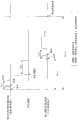
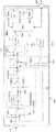
图1例示出本发明的第1实施方式的数据处理系统。虽没有特别限制,但该图所示的数据处理系统100构成为通过互补型MOS集成电路制造技术等而形成在单晶硅等的一个半导体衬底上的片上系统(System on a Chip)的半导体器件。数据处理系统100具有作为代表而示出的微型计算机(MCU)101、可编程增益放大器(PGA)102、以及选择器(SW1)103。虽然没有特别图示,但毫无疑问也可以集成有存储器和加速器等其他电路。FIG. 1 shows an example of a data processing system according to a first embodiment of the present invention. Although not particularly limited, the
虽没有特别限制,但微型计算机101具有:作为控制电路而执行程序的中央处理装置(CPU)110;能够电重写地存储程序和数据的闪存器等非易失性存储器(FLASH)111;在CPU110的工作区域等中利用的RAM112;将模拟信号转换成数字信号的AD转换电路(ADC)113;将数字信号转换成模拟信号的第1DA转换电路(DAC1)114;将数字信号转换成模拟信号的第2DA转换电路(DAC2)115;数字输入输出口116;模拟输入口117;计时器和串行接口等其他周边电路模块(PRPH)118;以及选择器(SW2)119。Although not particularly limited, the
CPU110通过信号120而进行针对可编程增益放大器102的增益的设定。第2DA转换电路115对从CPU110供给的放大器偏移数据进行DA转换而向可编程增益放大器102供给放大器偏移121。第2DA转换电路115对从CPU110供给的数据进行DA转换并将其输出。选择器103对从模拟输入口117供给的作为AD转换对象的被测定模拟信号123或从第1DA转换电路114输出的信号122进行选择并供给到可编程增益放大器102。选择器119对选择器103的输出或可编程增益放大器102的输出进行选择并供给到AD转换电路113。CPU110参考在AD转换电路113中进行转换而得到的数据。通过CPU110进行上述选择器103、119的开关控制。
图1主要着眼于相对于AD转换电路113的分辨率得到将其位精度扩展的AD转换结果的功能的结构。尤其能够根据CPU110的程序控制在AD转换电路113的输入量程的整个区域内提高其分辨率而得到AD转换结果。以下,详细说明其AD转换功能。FIG. 1 mainly focuses on the structure of the function of obtaining an AD conversion result whose bit precision is expanded with respect to the resolution of the
首先,说明本实施方式的AD转换的原理。First, the principle of AD conversion in this embodiment will be described.
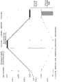
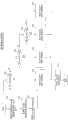
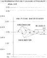
图2整体地例示出本实施方式的AD转换的原理。在此,使AD转换电路113的分辨率为10位。将转换精度扩展2位,与此相应地,将AD转换电路113的输入量程(为便于说明,使AD转换电路113的输入量程的电压范围为0.5V~4.5V)分割成四部分,按分割而成的各个电压范围即分割量程的区间(0.5V~1.5V,1.5V~2.5V,2.5V~3.5V,3.5V~4.5V)预先准备各分割量程的12位的数字偏移(DFS1、DFS2、DFS3、DFS4)。在对被测定模拟信号的AD转换动作中,在可编程增益放大器102中设定用于将被测定模拟信号所属的分割量程的区间的电压放大为AD转换电路113的输入量程的电压范围的放大器偏移和目的增益4(=22),从而将该被测定模拟信号放大至4倍。放大后的信号在AD转换电路113中转换成10位的数据,针对转换而成的10位的数据在低位侧进行2位的位扩展,例如进行2位的0扩展,对位扩展后的数据除以可编程增益放大器102的实测增益,由此,获得使该可编程增益放大器102的增益误差抵消后的该分割量程中的12位的AD转换数据。通过使该AD转换数据与对应的分割量程的12位的数字偏移(DFS1、DFS2、DFS3、DFS4)相加,能够得到位精度扩展至12位的AD转换数据。如上所述,通过对在被测定信号所属的分割量程得到的10位的AD转换数据进行2位的位扩展和由实测增益进行除法运算,能够使可编程增益放大器102的增益误差抵消,另外,各分割量程的数字偏移所确定的电压与低位侧的分割量程的最大电压一致,能够保证分割量程的各区间中的AD转换结果的连续性。以下,详细说明上述内容。FIG. 2 exemplifies the principle of AD conversion in this embodiment as a whole. Here, the resolution of the
首先,关于对可编程增益放大器102的放大器偏移的设定,如图3所例示,着眼于对整个量程分割成四部分后的区间2,当使电压Vx为区间2的最小电压时,若在使输入电压Va=Vx时、Vo=0V,并将从Vo=Va(R1+R2)/R1-VbR2/R1的关系式得到的电压Vb作为放大器偏移,则区间2的输入电压以该区间的电压范围成为AD转换电路113的输入量程的电压范围的方式放大。First, regarding the setting of the amplifier offset of the
例如图4及图5着眼于分割量程的区间而示出本实施方式的AD转换的原理。即,图4例示出,通过可编程增益放大器102将分割量程的区间2(在本例中为了便于说明,使AD转换电路113的输入量程的电压范围为0V~5V,不与图2的说明一致)的被测定模拟信号放大至4倍,将放大后的信号在AD转换电路113中转换成10位的数据,进行针对该数据的2位的0扩展和针对扩展后的数据由实测增益进行的除法运算,并使该结果与数字偏移DFS2相加,从而获取位精度扩展后的12位的AD转换数据时的原理。图5例示出,将分割量程的区间3(在本例中为了便于说明,使AD转换电路113的输入量程的电压范围为0V~5V,不与图2的说明一致)的被测定模拟信号放大至4倍后进行AD转换,进行针对AD转换后的10位的数据的低位侧2位的0扩展和针对扩展后的数据由实测增益进行的除法运算,并使该结果与数字偏移DFS3相加,从而获取位精度扩展后的12位的AD转换数据时的原理。For example, FIG. 4 and FIG. 5 show the principle of AD conversion in this embodiment focusing on the intervals of the divided ranges. That is, FIG. 4 illustrates that the
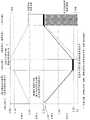
图6及图7同样地着眼于分割量程的区间而示出本实施方式的AD转换的原理,但在此特别示出在可编程增益放大器102保持放大动作的直线性的电压范围内使区间交错的情况,并与图2一致。作为可编程增益放大器102的一般特性,存在无法在最小输入电压及最大输入电压附近良好地保证放大动作的直线性的情况,为了避免增益误差增大而在相邻部分使区间交错。例如作为输入量程的10%而确保交错区间的电压范围分别为0.5V。例如在图6的区间3的例子中,只要以使2.5V~3.5V的区间3的输入电压范围成为0.5V~4.5V的量程的方式确定放大器偏移即可。区间3的数字偏移只要以使区间2的最大电压与区间3的最小电压一致的方式确定即可,其详细情况将在后说明。在图7的区间2的例子中,只要以使1.5V~2.5V的区间2的输入电压范围成为AD转换电路的输入量程的电压范围0.5V~4.5V的方式确定放大器偏移即可。区间2的数字偏移只要以使区间1的最大电压与区间2的最小电压一致的方式确定即可,其详细情况将在后说明。FIG. 6 and FIG. 7 similarly show the principle of AD conversion in this embodiment by focusing on the intervals of the divided ranges, but here, in particular, it is shown that the intervals are interleaved in the voltage range where the linearity of the amplification operation of the
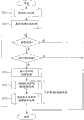
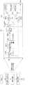
图8整体示出遵循上述原理的本实施方式的AD转换处理程序。该AD转换处理预先进行可编程增益放大器的增益校正处理(RT1)及数字偏移的计算处理(RT2),然后,只要不被指示中止执行本实施方式的AD转换处理且存在AD转换的指示,则基于被测定模拟信号进行输入区间的判断处理(RT3)、通过AD转换电路对被测定模拟信号进行AD转换处理(RT4)、以及针对AD转换处理(RT4)的结果进行增益修正及数字偏移相加处理(RT5)。AD转换处理(RT4)和增益修正及数字偏移相加处理(RT5)构成使针对被测定模拟信号判断出的区间成为AD转换电路113的输入量程的电压范围而进行AD转换的扩展AD转换处理。FIG. 8 generally shows the AD conversion processing procedure of the present embodiment based on the above principle. In this AD conversion process, the gain correction process (RT1) of the programmable gain amplifier and the calculation process (RT2) of the digital offset are performed in advance, and thereafter, as long as there is no instruction to suspend the execution of the AD conversion process of this embodiment and there is an AD conversion instruction, Then, based on the measured analog signal, the judgment process of the input interval is performed (RT3), the AD conversion process (RT4) is performed on the measured analog signal through the AD conversion circuit, and the gain correction and digital offset are performed on the result of the AD conversion process (RT4) Addition processing (RT5). The AD conversion processing (RT4) and the gain correction and digital offset addition processing (RT5) constitute extended AD conversion processing in which AD conversion is performed for the section determined for the analog signal to be measured to be within the voltage range of the input range of the
上述增益校正处理(RT1)根据将设定有目的增益(2n,例如n=2而为4倍)的可编程增益放大器102的输出在AD转换电路113中进行转换后的数字值与此时向可编程增益放大器102供给的用于生成模拟信号的数字值的差分,进行获取相对于目的增益的实测增益的处理。即,根据将从上述第1DA转换电路114输出的模拟信号通过上述可编程增益放大器102放大并在上述AD转换电路113中进行转换而得到的数据、和在不将上述模拟信号通过上述可编程增益放大器113放大的情况下在上述AD转换电路113中进行转换而得到的数据,运算并获取可编程增益放大器的增益。实测增益用于扩展AD转换处理中的增益修正。The above-mentioned gain correction process (RT1) is based on the digital value converted in the
上述输入区间的判断处理(RT3)为如下处理:判断基于上述AD转换电路113的对被测定模拟信号的转换结果是否属于将该AD转换电路113的输入量程分割成m(正整数)部分后的某一分割量程。例如,该判断处理(RT3)为根据与AD转换电路113的各分割量程的边界电压相应的电压的AD转换数据来判断被测定电压所属的输入量程的处理。The judgment processing (RT3) of the above-mentioned input interval is the following processing: judging whether the conversion result of the measured analog signal based on the above-mentioned
上述AD转换处理(RT4)为如下处理:与将判断出的分割量程的电压范围放大至上述AD转换电路的输入量程的电压范围的放大器偏移一起,作为目的增益而对上述可编程增益放大器102设定2n(在此n=2),并通过上述AD转换电路113对基于设定后的可编程增益放大器102而得到的上述被测定模拟信号的放大信号进行AD转换。The AD conversion process (RT4) is a process in which the
上述增益修正及数字偏移相加处理(RT5)为如下处理:在通过AD转换处理RT4而转换得到的10位数字数据的低位侧进行2位的0扩展,使扩展后的12位的数据由实测增益(相对于该目的增益2n的实测的增益)进行除法运算,并使除法运算得到的12位的数据和与对应的分割量程的最小电压相应的数字偏移数据相加,从而获取扩展有12位的转换精度的AD转换结果。The above-mentioned gain correction and digital offset addition processing (RT5) is the following processing: 2-bit 0-extension is performed on the low-order side of the 10-bit digital data converted by the AD conversion processing RT4, so that the extended 12-bit data is represented by The measured gain (relative to the measured gain of the target gain 2n ) is divided, and the 12-bit data obtained by the division is added to the digital offset data corresponding to the minimum voltage of the corresponding divided range to obtain the expansion AD conversion result with 12-bit conversion precision.
数字偏移生成处理(RT2)大致为图9所例示的作为基准的区间的数字偏移数据的生成处理、图10所例示的作为基准的区间的高位侧数字偏移数据的生成处理、以及图11所例示的作为基准的区间的低位侧数字偏移数据的生成处理。The digital offset generation process (RT2) is roughly the generation process of the digital offset data of the reference interval illustrated in FIG. 9, the generation process of the high-order side digital offset data of the reference interval illustrated in FIG. The generation process of the lower-order-side digital offset data of the reference section exemplified in 11.
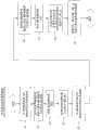
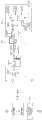
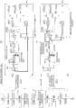
在图9所例示的数字偏移数据DFS2的生成处理中,首先,进行第1处理,即在上述第1DA转换电路114中生成特定的上述分割量程的任意电压(例如区间2的电压2.1V)(S1),将其经由选择器103、119的端子a、d提供给上述AD转换电路113而获取AD转换后的第1数据(S2)。由此,得到作为数字偏移数据DFS2的基础的10位的数据。CPU110进行第2处理,即读取该第1数据M2(S3),在所读取的第1数据M2的低位侧进行2位的0扩展而获取12位的第2数据M2-eb(S4)。然后,进行第3处理,即在上述第2DA转换电路115中生成将该分割量程的电压范围(1.5V~2.5V)放大至上述AD转换电路的输入量程(0.5V~4.5V)的电压范围的放大器偏移(S5),通过具有所生成的放大器偏移和处于目的增益附近的实测增益的上述可编程增益放大器102将在上述第1DA转换电路114中生成的上述任意电压放大,将放大后的信号在上述AD转换电路113中进行转换(S6),通过CPU110读取转换得到的第3数据A2(S7)。CPU110进行第4处理(S8),即在上述第3数据A2的低位侧进行2位的0扩展,由上述实测增益进行除法运算而获取第4数据A2-eb-g。最后,进行第5处理(S9),即从上述第2数据M2-eb减去第4数据A2-eb-g而获取该特定的分割量程的基准数字偏移数据DFS2(第5数据)。In the generation process of the digital offset data DFS2 illustrated in FIG. 9 , first, the first process is performed, that is, the first
根据图9的处理,数字偏移数据DFS2与不经由可编程增益放大器102而在AD转换电路113的输入量程的电压范围内将上述任意电压进行AD转换后的值实质一致。而且,在作为基准的区间的电压范围内,将对通过可编程增益放大器而放大的输入量程的电压范围进行AD转换后的结果扩展n位并由上述实测增益进行除法运算后的值和数字偏移数据DFS2相加,所得到的值与不经由可编程增益放大器而直接进行AD转换后的值实质一致。According to the processing of FIG. 9 , the digital offset data DFS2 substantially matches the value obtained by AD-converting the above-mentioned arbitrary voltage within the voltage range of the input range of the
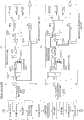
在图10所例示的位于区间2的高位侧的区间3的数字偏移数据DFS3的生成处理中,在生成上述数字偏移数据DFS2后,首先,进行第6处理,即在上述第1DA转换电路114中生成上述特定的分割量程的区间2的最大电压2.5V(S10),并且在上述第2DA转换电路115中生成将该分割量程(区间2)的电压范围(1.5V~2.5V)放大至上述AD转换电路113的输入量程的电压范围(0V~5V)的放大器偏移(S11),通过设定有所生成的放大器偏移和目的增益的上述可编程增益放大器102将在上述第1DA转换电路114中生成的区间2的最大电压2.5V放大,并将放大后的信号在上述AD转换电路113中进行转换(S12)而得到第6数据A2max(S13)。CPU110进行第7处理,即在第6数据A2max的低位侧进行2位的0扩展而生成临时的12位的数据(A2max-eb)(S14),使该数据A2max-eb由上述实测增益进行除法运算而生成数据A2max-eb-g(S15),并使该数据A2max-eb-g与上述数字偏移数据DFS2相加而获取作为12位的AD转换数据的第7数据A2max-12b(S16)。In the generation process of the digital offset data DFS3 of the interval 3 located on the higher side of the
然后,CPU110进行第8处理,即在上述第2DA转换电路115中生成将上述高位侧分割量程(区间3)的电压范围(2.5V~3.5V)放大至上述AD转换电路的输入量程的放大器偏移(S17),在上述AD转换电路113中对作为区间3的最小电压2.5V而放大后的信号进行转换(S18),从而获取第8数据A3min(S19)。最后,进行第9处理,即在第8数据A3min的低位侧进行2位的0扩展,由上述实测增益进行除法运算而生成数据A3min-eb-g(S20),从上述第7数据A2max-12b减去生成的数据A3min-eb-g而获取上述高位侧分割量程(区间3)的数字偏移数据DFS3(第9数据)(S21)。Then, the
由此,能够确保区间2的AD转换数据与区间3的AD转换数据的连续性。即,通过上述处理,由于使用已知的数字偏移数据DFS2进行运算从而使求出已知的数字偏移数据DFS2的特定分割量程(区间2)和与其相邻的高位侧分割量程(区间3)的连接点的电压(2.5V)在双方的分割量程内一致,所以能够保证特定分割量程(区间2)和与其相邻的高位侧分割量程(区间3)的连续性。换言之,在高位侧分割量程的电压范围内,将对通过可编程增益放大器而放大的输入量程的电压范围进行AD转换后的结果扩展n位并由上述实测增益进行除法运算后的值与上述数字偏移数据DFS3相加,所得到的值与不经由可编程增益放大器而直接进行AD转换后的值实质一致。尤其是,由于对在各个分割量程进行AD转换后的值进行n位的位扩展和针对该结果由实测增益进行的除法运算,所以能够排除可编程增益放大器102的增益误差的影响,从而能够高精度地保证其连续性。Thereby, the continuity of the AD converted data of the
此外,数字偏移数据DFS4只要根据已知的数字偏移数据DFS3通过与图10相同的处理求出即可,因此省略其详细说明。In addition, the digital offset data DFS4 has only to be obtained from the known digital offset data DFS3 by the same process as that of FIG. 10 , and thus a detailed description thereof will be omitted.
在图11所例示的已知的数字偏移数据DFS2的低位侧数字偏移数据DFS1的生成处理中,在生成上述数字偏移数据DFS2后,首先,进行第10处理,即在上述第1DA转换电路114中生成上述特定的分割量程(区间2)的最小电压(1.5V)(S22),并且在上述第2DA转换电路115中生成将该分割量程(区间2)的电压范围(1.5V~2.5V)放大至上述AD转换电路113的输入量程(0V~5V)的放大器偏移(S23),通过设定有所生成的放大器偏移和目的增益的上述可编程增益放大器102将在上述第1DA转换电路114中生成的最小电压2.5V放大,并将放大后的信号在上述AD转换电路113中进行转换(S24)而得到第10数据A2min(S25)。CPU110进行第11处理,即生成在第10数据A2min的低位侧进行2位的0扩展而得到的临时的12位的数据A2min-eb(S26),并且使该数据A2min-eb由上述实测增益进行除法运算而生成数据A2min-eb-g(S27),使该数据A2min-eb-g与上述数字偏移数据DFS2相加而得到作为12位的AD转换数据的第11数据(A2min-12b)(S28)。In the generation process of the lower-order side digital offset data DFS1 of the known digital offset data DFS2 shown in FIG. The
然后,CPU110进行第12处理,即在上述第1DA转换电路114中生成上述低位侧的分割量程(区间1)的最大电压(1.5V),并且在上述第2DA转换电路115中生成将该分割量程的电压范围(0.5V~1.5V)放大至上述AD转换电路113的输入量程(0V~5V)的放大器偏移(S29),通过设定有所生成的放大器偏移和目的增益的上述可编程增益放大器102将在上述第1DA转换电路114中生成的最大电压(1.5V)放大,并将放大后的信号在上述AD转换电路113中进行转换(S30)而得到第12数据A1max(S31)。最后,CPU110进行第13处理,即在上述第12数据A1max的低位侧进行2位的0扩展,由上述实测增益进行除法运算而生成数据A1max-eb-g(S32),从上述第11数据A2min-12b减去生成的数据A1max-eb-g而得到上述低位侧分割量程(区间1)的数字偏移数据DFS1(S33)。Then, the
由此,能够确保区间2的AD转换数据与区间1的AD转换数据的连续性。即,通过上述处理,由于使用已知的数字偏移数据DFS2进行运算从而使求出已知的数字偏移数据DFS2的特定分割量程(区间2)和与其相邻的低位侧分割量程(区间1)的连接点的电压(1.5V)在双方的分割量程内一致,所以能够确保特定分割量程(区间2)和与其相邻的低位侧分割量程(区间1)的连续性。换言之,在低位侧分割量程的电压范围内,将对通过可编程增益放大器而放大的输入量程的电压范围AD转换后的结果扩展n位并由上述实测增益进行除法运算后的值与上述数字偏移数据DFS1相加,所得到的值与不经由可编程增益放大器而直接进行AD转换后的值实质一致。尤其是,由于对在各个分割量程内进行AD转换后的值进行n位的位扩展和针对该结果由实测增益进行的除法运算,所以能够排除可编程增益放大器的增益误差的影响,从而能够高精度地保证其连续性。Thereby, the continuity of the AD converted data of the
图12例示出上述输入区间的判断处理(RT3)及上述AD转换处理(RT4)的详细情况。使选择器103选择输入端子b,使选择器119选择输入端子d(S40),在AD转换电路113中对被测定模拟信号进行AD转换(S41、S42)。CPU110读取该AD转换结果(S43),并判断该AD转换结果是否大于区间3与区间4的边界值(S44),若大于,则对放大器偏移用的DA转换寄存器设定区间4的放大器偏移数据(S45),并等待第1DA转换电路114的转换动作的稳定(S46)。当该AD转换结果小于区间3与区间4的边界值时,判断该AD转换结果是否大于区间2与区间3的边界值(S47),若大于,则对放大器偏移用的DA转换寄存器设定区间3的放大器偏移数据(S48),并等待第1DA转换电路114的转换动作的稳定(S49)。同样地,当该AD转换结果小于区间2与区间3的边界值时,判断该AD转换结果是否大于区间1与区间2的边界值(S50),若大于,则对放大器偏移用的DA转换寄存器设定区间2的放大器偏移数据(S51),并等待第1DA转换电路114的转换动作的稳定(S52)。同样地,当该AD转换结果小于区间1与区间2的边界值时,对放大器偏移用的DA转换寄存器设定区间1的放大器偏移数据(S53),并等待第1DA转换电路114的转换动作的稳定(S54)。在经过各自的稳定等待时间(例如3μs)后,使选择器119的输入与PGA102的输出连接(S55)。由此,与将判断出的分割量程的电压范围放大至上述AD转换电路113的输入量程的放大器偏移一起,作为目的增益而对上述可编程增益放大器102设定2n(在此增益为4),并通过上述AD转换电路113对基于设定后的可编程增益放大器102而得到的上述被测定模拟信号的放大信号进行转换处理。FIG. 12 exemplifies the details of the determination process ( RT3 ) of the input section and the AD conversion process ( RT4 ). The
图13例示出上述增益修正及数字偏移相加处理(RT5)的详细情况。CPU110对通过上述AD转换处理(RT4)在AD转换电路113中转换得到的数字数据,在其低位侧进行n位(在此为2位)的0扩展而生成12位的数据AE1(S60),并且对该数据AE1除以实测增益(S61),保持运算结果的数据(V1)并参照基于上述输入区间的判断处理(RT3)而得到的判断结果(S62)。若基于上述输入区间的判断处理(RT3)而得到的判断结果为区间4,则CPU110使运算结果数据V1与区间4的数字偏移相加(S63、S64),若基于上述输入区间的判断处理(RT3)而得到的判断结果为区间3,则CPU110使运算结果数据V1与区间3的数字偏移相加(S65、S66),若基于上述输入区间的判断处理(RT3)而得到的判断结果为区间2,则CPU110使运算结果数据V1与区间2的数字偏移相加(S67、S68),若基于上述输入区间的判断处理(RT3)而得到的判断结果为区间1,则CPU110使运算结果数据V1与区间1的数字偏移相加(S69),相加结果的数据保持为扩展至12位的AD转换结果(S70)。FIG. 13 exemplifies details of the above-mentioned gain correction and digital offset addition processing (RT5). The
图14例示出通过本实施方式的AD功能而进行的AD转换动作的时序图。如图所示,用于通过AD转换电路113而进行AD转换的被测定模拟信号的采样和AD转换动作按照上述输入区间判断用的动作(监控AD转换)、和扩展AD转换用的输入测定动作(正式AD转换)的顺序进行。在监控AD转换后,使用该结果进行分割区间的判断(OPR1),在正式AD转换后,进行位扩展、增益修正、以及数字偏移的附加等操作(OPR2)。例如在一次采样和转换中耗费2μs,能够在总计30μs中得到基于本实施方式的AD转换的扩展至12位的AD转换结果,因此,能够比普通的ΔΣAD转换器更高速地进行处理。FIG. 14 illustrates a timing chart of an AD conversion operation performed by the AD function of this embodiment. As shown in the figure, the sampling and AD conversion operations of the analog signal to be measured for AD conversion by the
根据以上说明的第1实施方式,能够根据对AD转换电路113的输入量程的分割数m而在满足2n≤m的关系的范围内最终得到n位的位扩展后的AD转换结果。此时,通过与从第2DA转换电路115向可编程增益放大器102提供使判断出的分割量程的范围成为AD转换电路113的整个量程的放大器偏移并进行放大的情况的一致性,可编程增益放大器102以增益2n或在其附近进行放大。由此,能够在AD转换电路113的转换量程的整个区域内提高其分辨率。即使在选择转换量程时,也不通过可编程增益放大器102进行放大而只要在AD转换电路113中进行一次AD转换来判断即可,因此,针对转换量程的切换也能够得到良好的跟踪性。而且,在各个分割量程的数字偏移中,由于分割量程的连接点的值在双方的分割量程中为同一值,所以能够在AD转换电路113的转换量程的整个区域内相对于高分辨率的AD转换结果减小转换误差。另外,由于对将分割量程的输入在AD转换电路113的输入量程的电压范围内进行AD转换而得到的数字数据进行位扩展,并使扩展后的数据由实测增益进行除法运算,所以能够排除可编程增益放大器的增益误差的影响。According to the first embodiment described above, an n-bit bit-extended AD conversion result can be finally obtained within the range satisfying the relationship of 2n ≤ m according to the division number m of the input range to the
《实施方式2》"
在实施方式2中,说明通过与实施方式1不同的方法而求出各个分割量程的数字偏移的处理。在此虽然没有特别图示,但能够是,例如,由于作为特定基准的区间的数字偏移与特定区间的最小电压实质一致,所以将特定区间的最小电压在AD转换电路113中进行AD转换,并使在低位侧进行2位的0扩展后的12位的数据成为作为基准的区间的数字偏移。例如从DAC1输出2.5V且在不通过PGA102进行放大的情况下通过ADC113进行AD转换,对转换结果数据进行下述2位的位扩展,从而使其成为作为基准的区间的数字偏移。In
由于上述特定区间的高位侧区间的数字偏移与上述特定区间的最大电压实质一致,所以能够将特定区间的最小电压在AD转换电路113中进行AD转换,在低位侧进行2位的0扩展并由实测增益进行除法运算,使该除法运算结果与已知的作为基准的区间的数字偏移数据相加,由此将所得到的12位的扩展AD转换结果作为其数字偏移。此外,能够根据该高位侧区间的已知的数字偏移通过相同的处理得到该高位侧区间的更高位侧区间的数字偏移。Since the digital offset of the high-order side interval of the above-mentioned specific interval is substantially consistent with the maximum voltage of the above-mentioned specific interval, the minimum voltage of the specific interval can be AD-converted in the
由于上述特定区间的低位侧区间的数字偏移与上述特定区间的最小电压的差分实质一致,所以能够将特定区间的最小电压在AD转换电路113中进行AD转换,在低位侧进行2位的0扩展并由实测增益进行除法运算,将该除法运算结果与已知的作为基准的区间的数字偏移数据的差分作为该数字偏移。此外,能够根据该低位侧区间的已知的数字偏移通过相同的处理得到该低位侧区间的更低位侧区间的数字偏移。Since the digital offset of the low-order side interval of the above-mentioned specific interval is substantially consistent with the difference of the minimum voltage of the above-mentioned specific interval, the minimum voltage of the specific interval can be AD-converted in the
根据实施方式2的处理,能够有助于提高获取数字偏移的处理效率。According to the processing of
《实施方式3》"Implementation Mode 3"
图15例示出本发明的第2实施方式的数据处理系统。该图所示的数据处理系统200与图1的数据处理系统100相比不同点在于:增加了采样保持电路201,采用了进行与其相应的控制的CPU110A。即,具有输入被测定模拟信号123的采样保持电路201,CPU110A使用被上述采样保持电路201采样的相同的被测定模拟信号123来进行分割量程的判断和利用了该判断结果的上述扩展AD转换用的处理。采样保持电路201具有采样开关(SMP1)211、采样电容(SC1)212、输出缓冲器(BUF)213及输出选择开关(SW3)214而构成。关于其他结构,对与图1相同的构成要素标注相同附图标记并省略其详细说明。FIG. 15 shows an example of a data processing system according to a second embodiment of the present invention. The
图16例示出被测定模拟信号的采样保持动作。在采样电容212中存储需要的电荷信号后,闭合采样开关211。Fig. 16 shows an example of the sample-and-hold operation of the analog signal to be measured. After the required charge signal is stored in the
图17例示出使保持于采样保持电路201的信息通过PGA102而在ADC113中进行AD转换的动作。使用通过该监控动作而得到的AD转换数据进行在图8中说明的输入区间的判断处理(RT3)及被测定电压AD转换处理(RT4)。FIG. 17 exemplifies the operation of performing AD conversion in the
图18例示出增益修正及数字偏移相加处理(RT5)中的动作。在该动作中只要从采样电容212接收被测定信号即可,不需要重新从外部输入被测定模拟信号。FIG. 18 shows an example of operations in the gain correction and digital offset addition processing ( RT5 ). In this operation, it is only necessary to receive the signal to be measured from the
根据第2实施方式,由于能够对相同的被测定模拟信号进行分割量程的判断和利用了该判断结果的上述AD转换,所以能够将发生误用不同的分割量程而进行AD转换的事态防患于未然。According to the second embodiment, since the determination of the divided range and the above-mentioned AD conversion using the judgment result can be performed on the same analog signal to be measured, it is possible to prevent the situation where AD conversion is performed by mistakenly using a different divided range. Not yet.
《实施方式4》"Implementation Mode 4"
在上述实施方式的说明中使输入量程的分割数m为4而进行了说明。即,当使基于本实施方式的AD而得到的AD转换结果的扩展位数n=2时,分割数为2n=22。理论上,分割数m能够在满足2n≤m的关系的范围内任意确定。In the description of the above embodiment, the number m of divisions of the input range has been described as four. That is, when the number of extension bits of the AD conversion result obtained by AD in this embodiment is n=2, the number of divisions is 2n =22 . Theoretically, the division number m can be determined arbitrarily within a range satisfying the relationship of 2n ≤ m.
此时,为了对在周期信号中作为代表的动态信号最大限度地利用AD转换电路的性能(分辨率),通常认为使动态信号的中点为AD转换电路的输入电压范围的二分之一不失为上策。在如上述实施方式所说明那样将输入量程分割的AD转换方式的情况下,当使分割数为偶数时,AD转换电路的输入电压范围的二分之一处成为相邻的分割量程的边界。在该方面,由于采用偶数或奇数的某一种来作为分割数m,所以在本实施方式的AD转换中产生处理效率的差。在第3实施方式中就该方面进行说明。At this time, in order to maximize the performance (resolution) of the AD conversion circuit for the dynamic signal represented by the periodic signal, it is generally considered that the midpoint of the dynamic signal is half of the input voltage range of the AD conversion circuit. Best policy. In the case of the AD conversion method in which the input range is divided as described in the above embodiment, when the number of divisions is an even number, half of the input voltage range of the AD conversion circuit becomes a boundary between adjacent divided ranges. In this regard, since either an even number or an odd number is used as the division number m, a difference in processing efficiency occurs in the AD conversion of the present embodiment. This point will be described in the third embodiment.
图19例示出在被测定模拟信号的中央值接近AD转换电路113的输入量程的中央值时将上述AD转换电路113的输入量程的分割数设定成偶数而进行本实施方式的AD转换处理的情况。通过图19得以明确,周期信号的中央值的电压2.5V成为区间2与区间3的边界电压。该情况下,在上述的实施方式的AD转换动作中,一个周期信号的值属于相邻的不同区间2、区间3双方,其结果为,必须根据被测定模拟信号的值来频繁地进行放大器偏移的切换,由此ADC113的稳定等待时间延长,基于本实施方式的AD的转换处理效率降低。FIG. 19 shows an example in which the AD conversion process of this embodiment is performed by setting the number of divisions of the input range of the
为了避免该情况,如图20所例示那样,CPU110(110A)只要以在被测定模拟信号的中央值接近AD转换电路113的输入量程的中央值时将上述AD转换电路113的输入量程的分割数设定成奇数例如分割成五部分而进行本实施方式的AD转换处理的方式进行控制即可。由此,能够抑制被测定模拟信号123的中央值处于分割量程的边界附近。因此,容易将被测定模拟信号的变化范围收纳于一个区间,不需要每当被测定模拟信号越过该中央值而变化时进行改变分割量程的处理,能够提高扩展上述位精度的AD转换处理的效率。In order to avoid this situation, as illustrated in FIG. 20 , the CPU 110 (110A) simply divides the input range of the
尤其在图20的例子中,各分割量程的电压范围与上述实施方式1同样地为1V,相对于扩展位数n=2使可编程增益放大器102的目的增益保持为22,基于AD转换器113的输入量程扩展为例如从0.1V至4.9V。总之,只要在输入量程的两端部分考虑与AD转换电路113的能力相应的富余即可。In particular, in the example of FIG. 20 , the voltage range of each divided range is 1 V as in the above-mentioned first embodiment, and the target gain of the
《实施方式5》"
图21例示出第4实施方式的数据处理系统。该图所示的数据处理系统300与图1的数据处理系统100相比不同点在于:增加了采样保持电路201,并且DA转换电路集成为一个DA转换电路(DAC1)114,DA转换电路114的输出能够经由选择器220而选择性地供给到PGA102或选择器103,采用进行与此相应的控制的CPU110B。即,设有:选择性地取代上述被测定模拟信号123而对设定用模拟信号122进行采样保持并将其输出到上述可编程增益放大器102的采样保持电路201;兼用于放大器偏移的生成和设定用模拟信号的生成的DA转换电路(DAC1)114;和选择器220,其选择将在上述DA转换电路114中生成的放大器偏移121向上述可编程增益放大器102输出的路径或将在上述DA转换电路中生成的设定用模拟信号122向上述采样保持电路201供给的路径。CPU110B通过上述放大器偏移121的生成和设定用模拟信号122的生成而分开使用DA转换电路114来进行选择器220的选择控制。采样保持电路201具有采样开关(SMP1)211、采样电容(SC1)212、输出缓冲器(BUF)213及输出选择开关(SW3)214而构成。关于其他结构,对与图1相同的构成要素标注相同附图标记并省略其详细说明。FIG. 21 illustrates an example of a data processing system according to a fourth embodiment. The difference between the
如第1及第2实施方式所说明那样在分别具有向可编程增益放大器102输出放大器偏移121的DA转换电路115、和选择性地取代上述被测定模拟信号而将设定用模拟信号122向上述可编程增益放大器102输出的DA转换电路114的情况下,由于能够并行地进行放大器偏移的设定和设定用模拟信号的生成,所以能够有助于提高获取数字偏移时的处理效率。另一方面,如第4实施方式所述,在采用兼用于放大器偏移的生成和设定用模拟信号的生成的DA转换电路114的情况下,必须串行地进行放大器偏移的设定和设定用模拟信号的生成,但通过DA转换电路的兼用能够有助于缩小电路规模。As described in the first and second embodiments, each has a
通过将DA转换电路集成为一个,对PGA102的增益校正只要例如如图22的概要所示那样按顺序进行处理RT10至RT16即可。即,在图22所例示的实测增益获取处理中,使选择器103的端子为a,使选择器220为g,通过DA转换电路114输出模拟电压x1,使内置于采样保持电路201的开关211(SMP1)接通,使开关214(SW3)断开,在电容212(SC1)中保存电压x1(RT10)。在保存电压x1后,使开关211断开,使开关214接通,将选择器220设定为f,通过DA转换电路114输出任意电压O(例如0V)来作为PGA102的放大器偏移。By integrating the DA conversion circuit into one, the gain correction of the
使选择器119的端子为d,通过AD转换电路113在没有PGA102的路径上对保存于电容212的电压x1进行AD转换,得到AD转换结果y1(RT11)。然后使选择器119的端子为c,通过AD转换电路113在PGA102中将保存于电容212的电压x1放大,进行AD转换而得到AD转换结果Y1(RT12)。The terminal of the
同样地通过DA转换电路114输出模拟电压x2,在采样保持电路201中保存电压x2(RT13),在保存电压x2后,使开关211断开,使开关214接通,将选择器220设定为f,通过DA转换电路114输出上述放大器偏移电压O。Similarly, the analog voltage x2 is output through the
通过AD转换电路113在没有PGA102的路径上对存储于电容212的电压x2进行AD转换而获取AD转换结果y2(RT14),然后通过AD转换器113对PGA102所放大的电压x2进行AD转换而得到结果Y2(TR15)。The
最后CPU110B根据G=(Y2-Y1)/(y2-y1)对PGA102的实测增益G进行运算而获取实测增益(RT16)。像这样,针对不同的两个电压根据没有PGA102的路径上的AD转换结果和由PGA102放大的电压的AD转换结果的比率计算出实测增益G。Finally,
此外,在上述内容中使x1<x2而进行处理。另外,x1及x2的电压能够在通过PGA102而放大后的电压不超过AD转换电路的输入量程的范围内任意选择。In addition, in the above-mentioned content, x1<x2 is satisfied and processing is performed. In addition, the voltages of x1 and x2 can be arbitrarily selected within a range in which the voltage amplified by the
图23例示出处理RT10和RT11的详细情况。图24例示出处理RT12的详细情况。图25例示出处理RT13和RT14的详细情况。图26例示出处理RT15的详细情况。图27例示出计算区间3的数字偏移时的流程图中的A及B部分的详细情况,图28例示出计算区间3的数字偏移时的流程图中的C部分的详细情况。关于其他区间的数字偏移的计算流程省略了图示,但只要通过参照图27及图28的处理而生成即可。Fig. 23 exemplifies the details of processing RT10 and RT11. Fig. 24 exemplifies the details of processing RT12. Fig. 25 exemplifies the details of processing RT13 and RT14. Fig. 26 exemplifies the details of processing RT15. FIG. 27 exemplifies the details of parts A and B of the flowchart for calculating the digital offset of section 3, and FIG. 28 shows the details of section C of the flowchart for calculating the digital offset of section 3. The calculation flow of the digital offset in other sections is omitted from the illustration, but it only needs to be generated by the process referring to FIG. 27 and FIG. 28 .
以上根据实施方式具体说明了本发明人所完成的发明,但本发明不限定于此,毫无疑问在不脱离其要旨的范围内能够进行各种变更。As mentioned above, although the invention made by this inventor was concretely demonstrated based on embodiment, this invention is not limited to this, It cannot be overemphasized that various changes are possible in the range which does not deviate from the summary.
例如,通过微型计算机这样的控制部而进行的位扩展和由实测增益进行除法运算的处理不仅可以通过固定小数点运算而进行,也可以通过浮动小数点运算而进行。在数字偏移的生成处理等中进行用于扩展位精度的位扩展处理和由实测增益进行除法运算的顺序基本在进行位扩展后进行除法运算,在运算法则方面优选的情况需要按该顺序进行,但根据运算方法若不为该情况也可以相反。AD转换电路的位精度、扩展位数、区间的分割数不限定于上述实施方式,能够适当变更。另外,数据处理系统不限定于单芯片的半导体器件,也能够由多芯片构成。例如也能够使微型计算机(MCU)101、101A、101B由单芯片构成,并使其他电路由外置部件构成。For example, the processing of bit extension and division by an actual measurement gain performed by a control unit such as a microcomputer may be performed not only by fixed decimal point calculation but also by floating decimal point calculation. In the digital offset generation process, etc., the order of performing bit extension processing for extending the bit accuracy and dividing by the measured gain is basically performed after performing bit extension. When the algorithm is preferable, it is necessary to perform this order. , but it can also be reversed if it is not the case according to the calculation method. The bit precision of the AD conversion circuit, the number of extension bits, and the number of section divisions are not limited to the above-described embodiments, and can be changed as appropriate. In addition, the data processing system is not limited to a single-chip semiconductor device, and may be composed of multiple chips. For example, it is also possible to configure the microcomputers (MCU) 101 , 101A, and 101B by a single chip, and configure other circuits by external components.
上述各个实施方式也能够相互组合而构成。The above-mentioned respective embodiments can also be configured in combination with each other.
工业实用性Industrial Applicability
本发明涉及具有AD转换功能的数据处理系统,尤其能够在用于得到比AD转换电路的位精度更高的位精度的技术中广泛适用。The present invention relates to a data processing system having an AD conversion function, and is particularly widely applicable to techniques for obtaining bit precision higher than that of an AD conversion circuit.
附图标记说明Explanation of reference signs
100 数据处理系统100 data processing system
101 微型计算机(MCU)101 Microcomputer (MCU)
102 可编程增益放大器(PGA)102 Programmable Gain Amplifier (PGA)
103 选择器(SW1)103 Selector (SW1)
110 中央处理装置(CPU)110 Central processing unit (CPU)
111 非易失性存储器(FLASH)111 Non-volatile memory (FLASH)
112 RAM112 RAM
113 AD转换电路(ADC)113 AD conversion circuit (ADC)
114 第1DA转换电路(DAC1)114 The first DA conversion circuit (DAC1)
115 第2DA转换电路(DAC2)115 The second DA conversion circuit (DAC2)
116 数字输入输出口116 digital input and output ports
117 模拟输入口117 Analog input port
118 周边电路模块(PRPH)118 Peripheral circuit module (PRPH)
119 选择器(SW2)119 Selector (SW2)
200 数据处理系统200 data processing system
201 采样保持电路201 sample and hold circuit
110A CPU110A CPU
101A 微型计算机101A Microcomputer
300 数据处理系统300 data processing system
110B CPU110B CPU
101B 微型计算机101B microcomputer
Claims (25)
Applications Claiming Priority (3)
| Application Number | Priority Date | Filing Date | Title |
|---|---|---|---|
| JP2011-095819 | 2011-04-22 | ||
| JP2011095819 | 2011-04-22 | ||
| PCT/JP2012/059758WO2012144375A1 (en) | 2011-04-22 | 2012-04-10 | Data processing system |
Publications (2)
| Publication Number | Publication Date |
|---|---|
| CN103493378Atrue CN103493378A (en) | 2014-01-01 |
| CN103493378B CN103493378B (en) | 2016-10-12 |
Family
ID=47041487
Family Applications (1)
| Application Number | Title | Priority Date | Filing Date |
|---|---|---|---|
| CN201280019587.XAActiveCN103493378B (en) | 2011-04-22 | 2012-04-10 | Data handling system |
Country Status (4)
| Country | Link |
|---|---|
| US (3) | US8860593B2 (en) |
| JP (1) | JP5657783B2 (en) |
| CN (1) | CN103493378B (en) |
| WO (1) | WO2012144375A1 (en) |
Cited By (6)
| Publication number | Priority date | Publication date | Assignee | Title |
|---|---|---|---|---|
| CN107976647A (en)* | 2018-01-24 | 2018-05-01 | 镇江市计量实验工厂 | A kind of high-voltage high resistance calibrating instrument intelligence calibrating installation |
| CN108736851A (en)* | 2017-04-19 | 2018-11-02 | 中芯国际集成电路制造(上海)有限公司 | A kind of programmable gain amplifier and electronic device |
| CN109124637A (en)* | 2017-06-27 | 2019-01-04 | 瑞萨电子株式会社 | Height measuring device, health care facility and pivot gate |
| CN111193510A (en)* | 2018-11-14 | 2020-05-22 | 华为技术有限公司 | Data conversion device, system and method |
| CN112234991A (en)* | 2020-09-18 | 2021-01-15 | 芯创智(北京)微电子有限公司 | High-precision incremental analog-to-digital converter and conversion method thereof |
| CN113659987A (en)* | 2021-08-20 | 2021-11-16 | 合肥御微半导体技术有限公司 | Signal processing device and method thereof |
Families Citing this family (17)
| Publication number | Priority date | Publication date | Assignee | Title |
|---|---|---|---|---|
| WO2012144375A1 (en)* | 2011-04-22 | 2012-10-26 | ルネサスエレクトロニクス株式会社 | Data processing system |
| EP2936687A1 (en)* | 2012-12-18 | 2015-10-28 | Apator Miitors ApS | Utility meter controlling the conversion range of an adc |
| US10056924B2 (en) | 2013-08-19 | 2018-08-21 | Analog Devices, Inc. | High output power digital-to-analog converter system |
| US8970418B1 (en)* | 2013-08-19 | 2015-03-03 | Analog Devices, Inc. | High output power digital-to-analog converter system |
| CN103995226B (en)* | 2013-12-27 | 2017-01-04 | 杭州长川科技股份有限公司 | For the method improving analog integrated circuit test system precision |
| US9706269B2 (en)* | 2015-07-24 | 2017-07-11 | Hong Kong Applied Science and Technology Research Institute Company, Limited | Self-powered and battery-assisted CMOS wireless bio-sensing IC platform |
| JP6486237B2 (en)* | 2015-08-06 | 2019-03-20 | アズビル株式会社 | AD converter |
| US10079989B2 (en) | 2015-12-15 | 2018-09-18 | Ricoh Company, Ltd. | Image capturing device |
| US10098684B2 (en)* | 2016-04-06 | 2018-10-16 | Biosense Webster (Israel) Ltd. | Uncalibrated thermocouple system |
| US9774343B1 (en)* | 2016-07-13 | 2017-09-26 | The Boeing Company | Method and apparatus for improving the resolution of digitally sampled analog data |
| US10224945B2 (en)* | 2017-04-21 | 2019-03-05 | Aerobits Sp. z o.o. | Method for real time processing of fast analogue signals and a system for application thereof |
| KR102180180B1 (en)* | 2019-07-19 | 2020-11-18 | 엘지전자 주식회사 | Resolution control apparatus and resolution control method |
| KR102217903B1 (en)* | 2019-11-19 | 2021-02-19 | 엘아이지넥스원 주식회사 | Apparatus and Method for Signal Measuring using Signal Measuring Circuit |
| DE102020102647B4 (en) | 2020-02-03 | 2024-12-24 | Hanon Systems | Arrangement and method for generating an amplification signal for measuring amplifiers |
| CN112994636B (en)* | 2021-02-04 | 2024-03-29 | 珠海市丰润自动化科技有限公司 | Dead weight eliminating method, storage medium and terminal |
| EP4099572A1 (en) | 2021-05-31 | 2022-12-07 | Infineon Technologies AG | Environmental sensor |
| CN117632854B (en)* | 2023-11-29 | 2024-08-06 | 上海合芯数字科技有限公司 | Data processing method, device and equipment |
Citations (10)
| Publication number | Priority date | Publication date | Assignee | Title |
|---|---|---|---|---|
| US5422643A (en)* | 1993-02-24 | 1995-06-06 | Antel Optronics Inc. | High dynamic range digitizer |
| US6252536B1 (en)* | 1999-03-31 | 2001-06-26 | Cirrus Logic, Inc. | Dynamic range extender apparatus, system, and method for digital image receiver system |
| US20030102994A1 (en)* | 2001-06-08 | 2003-06-05 | Eric Stimmann | High dynamic range digital converter |
| US6791484B1 (en)* | 2003-07-18 | 2004-09-14 | National Semiconductor Corporation | Method and apparatus of system offset calibration with overranging ADC |
| TWI250749B (en)* | 2002-12-24 | 2006-03-01 | Realtek Semiconductor Corp | QAM receiver having joint gain, carrier recovery and equalization adaptation system and method thereof |
| TW200704154A (en)* | 2005-07-12 | 2007-01-16 | Pixart Imaging Inc | Reading circuit of image sensor and analog/digital conversion method thereof |
| US20080129563A1 (en)* | 2006-12-05 | 2008-06-05 | Alastair Mark Boomer | Calibration circuit and associated method |
| TW200830727A (en)* | 2006-07-24 | 2008-07-16 | Qualcomm Inc | Saturation detection for analog-to-digital converter |
| US7643573B2 (en)* | 2006-03-17 | 2010-01-05 | Cirrus Logic, Inc. | Power management in a data acquisition system |
| CN102422538A (en)* | 2009-05-29 | 2012-04-18 | 三菱电机株式会社 | Analog unit |
Family Cites Families (13)
| Publication number | Priority date | Publication date | Assignee | Title |
|---|---|---|---|---|
| JPS58127429A (en) | 1982-01-25 | 1983-07-29 | Hitachi Ltd | A/D conversion expansion method |
| JPH04370801A (en) | 1991-06-19 | 1992-12-24 | Matsushita Electric Ind Co Ltd | Analog signal detector |
| JPH0514201A (en) | 1991-06-27 | 1993-01-22 | Tdk Corp | A/d converter |
| JPH06334523A (en) | 1993-05-20 | 1994-12-02 | Jeco Co Ltd | Analog-digital converting device |
| US7142486B2 (en)* | 2001-04-02 | 2006-11-28 | Ricoh Company, Ltd. | Signal processing method and signal processing apparatus |
| US6975251B2 (en)* | 2002-06-20 | 2005-12-13 | Dakota Technologies, Inc. | System for digitizing transient signals with waveform accumulator |
| US7215266B2 (en)* | 2004-05-21 | 2007-05-08 | Wionics Research | Hybrid DC offset cancellation scheme for wireless receiver |
| US7405683B1 (en)* | 2004-05-27 | 2008-07-29 | Cypress Semiconductor Corporation | Extending the dynamic range in an energy measurement device |
| JP2006121146A (en)* | 2004-10-19 | 2006-05-11 | Renesas Technology Corp | Filter control apparatus and method of wireless receiver, and integrated circuit for wireless receiver employing the same |
| FR2938081B1 (en)* | 2008-10-31 | 2020-09-11 | Thales Sa | PROCESS FOR CORRECTING THE OFF-CENTERS IN AMPLITUDE AND IN PHASE OF A SIGMA-DELTA MODULATOR AND MODULATOR IMPLEMENTING THE PROCESS |
| JP5465965B2 (en)* | 2009-03-31 | 2014-04-09 | ルネサスエレクトロニクス株式会社 | Data processing apparatus and data processing system |
| WO2012144375A1 (en)* | 2011-04-22 | 2012-10-26 | ルネサスエレクトロニクス株式会社 | Data processing system |
| JP5779511B2 (en)* | 2012-01-20 | 2015-09-16 | ルネサスエレクトロニクス株式会社 | Semiconductor integrated circuit device |
- 2012
- 2012-04-10WOPCT/JP2012/059758patent/WO2012144375A1/enactiveApplication Filing
- 2012-04-10CNCN201280019587.XApatent/CN103493378B/enactiveActive
- 2012-04-10JPJP2013510956Apatent/JP5657783B2/enactiveActive
- 2012-04-10USUS14/113,213patent/US8860593B2/enactiveActive
- 2014
- 2014-08-13USUS14/458,406patent/US9065467B2/enactiveActive
- 2015
- 2015-06-22USUS14/745,627patent/US9337858B2/enactiveActive
Patent Citations (10)
| Publication number | Priority date | Publication date | Assignee | Title |
|---|---|---|---|---|
| US5422643A (en)* | 1993-02-24 | 1995-06-06 | Antel Optronics Inc. | High dynamic range digitizer |
| US6252536B1 (en)* | 1999-03-31 | 2001-06-26 | Cirrus Logic, Inc. | Dynamic range extender apparatus, system, and method for digital image receiver system |
| US20030102994A1 (en)* | 2001-06-08 | 2003-06-05 | Eric Stimmann | High dynamic range digital converter |
| TWI250749B (en)* | 2002-12-24 | 2006-03-01 | Realtek Semiconductor Corp | QAM receiver having joint gain, carrier recovery and equalization adaptation system and method thereof |
| US6791484B1 (en)* | 2003-07-18 | 2004-09-14 | National Semiconductor Corporation | Method and apparatus of system offset calibration with overranging ADC |
| TW200704154A (en)* | 2005-07-12 | 2007-01-16 | Pixart Imaging Inc | Reading circuit of image sensor and analog/digital conversion method thereof |
| US7643573B2 (en)* | 2006-03-17 | 2010-01-05 | Cirrus Logic, Inc. | Power management in a data acquisition system |
| TW200830727A (en)* | 2006-07-24 | 2008-07-16 | Qualcomm Inc | Saturation detection for analog-to-digital converter |
| US20080129563A1 (en)* | 2006-12-05 | 2008-06-05 | Alastair Mark Boomer | Calibration circuit and associated method |
| CN102422538A (en)* | 2009-05-29 | 2012-04-18 | 三菱电机株式会社 | Analog unit |
Cited By (9)
| Publication number | Priority date | Publication date | Assignee | Title |
|---|---|---|---|---|
| CN108736851A (en)* | 2017-04-19 | 2018-11-02 | 中芯国际集成电路制造(上海)有限公司 | A kind of programmable gain amplifier and electronic device |
| CN108736851B (en)* | 2017-04-19 | 2022-06-28 | 中芯国际集成电路制造(上海)有限公司 | Programmable gain amplifier and electronic device |
| CN109124637A (en)* | 2017-06-27 | 2019-01-04 | 瑞萨电子株式会社 | Height measuring device, health care facility and pivot gate |
| CN107976647A (en)* | 2018-01-24 | 2018-05-01 | 镇江市计量实验工厂 | A kind of high-voltage high resistance calibrating instrument intelligence calibrating installation |
| CN111193510A (en)* | 2018-11-14 | 2020-05-22 | 华为技术有限公司 | Data conversion device, system and method |
| CN112234991A (en)* | 2020-09-18 | 2021-01-15 | 芯创智(北京)微电子有限公司 | High-precision incremental analog-to-digital converter and conversion method thereof |
| CN112234991B (en)* | 2020-09-18 | 2024-05-17 | 芯创智(北京)微电子有限公司 | High-precision incremental analog-to-digital converter and conversion method thereof |
| CN113659987A (en)* | 2021-08-20 | 2021-11-16 | 合肥御微半导体技术有限公司 | Signal processing device and method thereof |
| CN113659987B (en)* | 2021-08-20 | 2023-07-11 | 合肥御微半导体技术有限公司 | Signal processing device and method thereof |
Also Published As
| Publication number | Publication date |
|---|---|
| US20150288377A1 (en) | 2015-10-08 |
| US9337858B2 (en) | 2016-05-10 |
| US9065467B2 (en) | 2015-06-23 |
| US20140055291A1 (en) | 2014-02-27 |
| WO2012144375A1 (en) | 2012-10-26 |
| US20140347199A1 (en) | 2014-11-27 |
| JPWO2012144375A1 (en) | 2014-07-28 |
| JP5657783B2 (en) | 2015-01-21 |
| CN103493378B (en) | 2016-10-12 |
| US8860593B2 (en) | 2014-10-14 |
Similar Documents
| Publication | Publication Date | Title |
|---|---|---|
| CN103493378B (en) | Data handling system | |
| US8717221B2 (en) | Successive approximation register analog-to-digital converter | |
| JP4160629B2 (en) | AD converter, AD conversion method, AD conversion program, and control apparatus | |
| TWI434517B (en) | Method, device and application of successive approximation register analog-to-digital converter for weighting of elements of digital analog converter | |
| US20100123611A1 (en) | Successive approximation register analog-digital converter and method of driving the same | |
| US9054732B2 (en) | SAR analog-to-digital conversion method and SAR analog-to-digital conversion circuit | |
| US8542144B2 (en) | Analog to digital converter | |
| KR101644999B1 (en) | Low-Power Analog Digital Converter By Using Time-Domain Multi-Stage Interpolation | |
| JP2001177410A (en) | High precision DA conversion circuit | |
| JP2008104142A (en) | Analog-to-digital converter | |
| US7403149B2 (en) | Folding and interpolating analog-to-digital converter and method of converting analog signal to digital signal | |
| CN101729067B (en) | Calibration device and method for pipeline analog-to-digital converter | |
| JP4140528B2 (en) | A / D converter | |
| WO2009122656A1 (en) | Pipeline type a-d converter | |
| JP2012227775A (en) | Analog-digital converter and signal processing system | |
| JP2001024509A (en) | Self-correction charge redistribution successive approximation AD converter | |
| US6700523B2 (en) | Analog to digital converter selecting reference voltages in accordance with feedback from prior stages | |
| JP4684028B2 (en) | Pipeline A / D converter | |
| KR20150072972A (en) | Analog to Digital Converter for interpolation using Calibration of Clock | |
| JP2005304033A (en) | Digitally self-calibrating pipelined ADC and method | |
| US10623011B2 (en) | Successive approximation analog-to-digital converter and calibration method thereof | |
| KR20130003545A (en) | Folded reference flash adc and method thereof | |
| KR100667907B1 (en) | Analog to digital converter | |
| KR101884114B1 (en) | ADC with Reference Voltage Scaling Scheme | |
| JP2012044533A (en) | A/d converter |
Legal Events
| Date | Code | Title | Description |
|---|---|---|---|
| C06 | Publication | ||
| PB01 | Publication | ||
| C10 | Entry into substantive examination | ||
| SE01 | Entry into force of request for substantive examination | ||
| CB02 | Change of applicant information | Address after:Tokyo, Japan, Japan Applicant after:Renesas Electronics Corporation Address before:Kanagawa Applicant before:Renesas Electronics Corporation | |
| COR | Change of bibliographic data | ||
| C14 | Grant of patent or utility model | ||
| GR01 | Patent grant |