CN103489838A - Enhanced radiation three-dimensional packaging structure and packaging method for same - Google Patents
Enhanced radiation three-dimensional packaging structure and packaging method for sameDownload PDFInfo
- Publication number
- CN103489838A CN103489838ACN201310481621.1ACN201310481621ACN103489838ACN 103489838 ACN103489838 ACN 103489838ACN 201310481621 ACN201310481621 ACN 201310481621ACN 103489838 ACN103489838 ACN 103489838A
- Authority
- CN
- China
- Prior art keywords
- substrate
- heat
- packaging structure
- heat dissipation
- microchannel
- Prior art date
- Legal status (The legal status is an assumption and is not a legal conclusion. Google has not performed a legal analysis and makes no representation as to the accuracy of the status listed.)
- Granted
Links
- 238000004806packaging method and processMethods0.000titleclaimsabstractdescription46
- 238000000034methodMethods0.000titleclaimsabstractdescription23
- 230000005855radiationEffects0.000titledescription2
- 239000000758substrateSubstances0.000claimsabstractdescription72
- XLYOFNOQVPJJNP-UHFFFAOYSA-NwaterSubstancesOXLYOFNOQVPJJNP-UHFFFAOYSA-N0.000claimsabstractdescription25
- 238000010438heat treatmentMethods0.000claimsabstractdescription23
- 229910052751metalInorganic materials0.000claimsabstractdescription17
- 239000002184metalSubstances0.000claimsabstractdescription17
- 239000004020conductorSubstances0.000claimsabstractdescription9
- 230000008569processEffects0.000claimsabstractdescription5
- 239000010410layerSubstances0.000claimsdescription32
- 238000001816coolingMethods0.000claimsdescription23
- 238000005516engineering processMethods0.000claimsdescription19
- 239000000463materialSubstances0.000claimsdescription11
- 238000013461designMethods0.000claimsdescription10
- 238000009826distributionMethods0.000claimsdescription7
- LYCAIKOWRPUZTN-UHFFFAOYSA-NEthylene glycolChemical compoundOCCOLYCAIKOWRPUZTN-UHFFFAOYSA-N0.000claimsdescription6
- 239000007788liquidSubstances0.000claimsdescription6
- 239000002356single layerSubstances0.000claimsdescription6
- PEDCQBHIVMGVHV-UHFFFAOYSA-NGlycerineChemical compoundOCC(O)COPEDCQBHIVMGVHV-UHFFFAOYSA-N0.000claimsdescription4
- XEEYBQQBJWHFJM-UHFFFAOYSA-NIronChemical compound[Fe]XEEYBQQBJWHFJM-UHFFFAOYSA-N0.000claimsdescription4
- PXHVJJICTQNCMI-UHFFFAOYSA-NNickelChemical compound[Ni]PXHVJJICTQNCMI-UHFFFAOYSA-N0.000claimsdescription4
- 229910052802copperInorganic materials0.000claimsdescription4
- 239000010949copperSubstances0.000claimsdescription4
- 229910052737goldInorganic materials0.000claimsdescription4
- 239000010931goldSubstances0.000claimsdescription4
- 229910052709silverInorganic materials0.000claimsdescription4
- WABPQHHGFIMREM-UHFFFAOYSA-Nlead(0)Chemical compound[Pb]WABPQHHGFIMREM-UHFFFAOYSA-N0.000claimsdescription3
- RYGMFSIKBFXOCR-UHFFFAOYSA-NCopperChemical compound[Cu]RYGMFSIKBFXOCR-UHFFFAOYSA-N0.000claimsdescription2
- LFQSCWFLJHTTHZ-UHFFFAOYSA-NEthanolChemical compoundCCOLFQSCWFLJHTTHZ-UHFFFAOYSA-N0.000claimsdescription2
- FYYHWMGAXLPEAU-UHFFFAOYSA-NMagnesiumChemical compound[Mg]FYYHWMGAXLPEAU-UHFFFAOYSA-N0.000claimsdescription2
- BQCADISMDOOEFD-UHFFFAOYSA-NSilverChemical compound[Ag]BQCADISMDOOEFD-UHFFFAOYSA-N0.000claimsdescription2
- RTAQQCXQSZGOHL-UHFFFAOYSA-NTitaniumChemical compound[Ti]RTAQQCXQSZGOHL-UHFFFAOYSA-N0.000claimsdescription2
- 239000000956alloySubstances0.000claimsdescription2
- 229910052782aluminiumInorganic materials0.000claimsdescription2
- XAGFODPZIPBFFR-UHFFFAOYSA-NaluminiumChemical compound[Al]XAGFODPZIPBFFR-UHFFFAOYSA-N0.000claimsdescription2
- 229910017052cobaltInorganic materials0.000claimsdescription2
- 239000010941cobaltSubstances0.000claimsdescription2
- GUTLYIVDDKVIGB-UHFFFAOYSA-Ncobalt atomChemical compound[Co]GUTLYIVDDKVIGB-UHFFFAOYSA-N0.000claimsdescription2
- 235000011187glycerolNutrition0.000claimsdescription2
- PCHJSUWPFVWCPO-UHFFFAOYSA-NgoldChemical compound[Au]PCHJSUWPFVWCPO-UHFFFAOYSA-N0.000claimsdescription2
- 229910052742ironInorganic materials0.000claimsdescription2
- 239000011133leadSubstances0.000claimsdescription2
- 229910052749magnesiumInorganic materials0.000claimsdescription2
- 239000011777magnesiumSubstances0.000claimsdescription2
- WPBNNNQJVZRUHP-UHFFFAOYSA-Lmanganese(2+);methyl n-[[2-(methoxycarbonylcarbamothioylamino)phenyl]carbamothioyl]carbamate;n-[2-(sulfidocarbothioylamino)ethyl]carbamodithioateChemical compound[Mn+2].[S-]C(=S)NCCNC([S-])=S.COC(=O)NC(=S)NC1=CC=CC=C1NC(=S)NC(=O)OCWPBNNNQJVZRUHP-UHFFFAOYSA-L0.000claimsdescription2
- 229910052759nickelInorganic materials0.000claimsdescription2
- 239000004332silverSubstances0.000claimsdescription2
- 239000010936titaniumSubstances0.000claimsdescription2
- 229910052719titaniumInorganic materials0.000claimsdescription2
- 238000012856packingMethods0.000claims2
- 239000004411aluminiumSubstances0.000claims1
- 239000004568cementSubstances0.000claims1
- 239000012809cooling fluidSubstances0.000claims1
- 238000009795derivationMethods0.000claims1
- 238000003475laminationMethods0.000claims1
- 230000017525heat dissipationEffects0.000abstractdescription51
- 238000012546transferMethods0.000abstractdescription10
- 238000011161developmentMethods0.000abstractdescription7
- 238000005538encapsulationMethods0.000abstractdescription6
- 238000012545processingMethods0.000abstractdescription6
- 238000004891communicationMethods0.000abstractdescription5
- 239000000919ceramicSubstances0.000description6
- 230000004907fluxEffects0.000description6
- 230000010354integrationEffects0.000description5
- 238000004519manufacturing processMethods0.000description5
- 238000004377microelectronicMethods0.000description5
- 239000003292glueSubstances0.000description4
- 230000001965increasing effectEffects0.000description4
- 230000008901benefitEffects0.000description3
- 239000000110cooling liquidSubstances0.000description3
- 239000000945fillerSubstances0.000description3
- 238000005553drillingMethods0.000description2
- 230000002708enhancing effectEffects0.000description2
- 238000012536packaging technologyMethods0.000description2
- 239000010944silver (metal)Substances0.000description2
- 238000003466weldingMethods0.000description2
- 230000005679Peltier effectEffects0.000description1
- 230000005540biological transmissionEffects0.000description1
- 230000015572biosynthetic processEffects0.000description1
- 238000005219brazingMethods0.000description1
- 239000003990capacitorSubstances0.000description1
- 238000000151depositionMethods0.000description1
- 238000010586diagramMethods0.000description1
- 230000000694effectsEffects0.000description1
- 238000005530etchingMethods0.000description1
- 230000006870functionEffects0.000description1
- 238000009413insulationMethods0.000description1
- 239000011229interlayerSubstances0.000description1
- 238000012423maintenanceMethods0.000description1
- 239000012528membraneSubstances0.000description1
- 238000001465metallisationMethods0.000description1
- 238000012986modificationMethods0.000description1
- 230000004048modificationEffects0.000description1
- 239000013307optical fiberSubstances0.000description1
- 239000012188paraffin waxSubstances0.000description1
- 238000003825pressingMethods0.000description1
- 238000003672processing methodMethods0.000description1
- 238000004080punchingMethods0.000description1
- 239000002994raw materialSubstances0.000description1
- 230000009467reductionEffects0.000description1
- 239000003507refrigerantSubstances0.000description1
- 238000005057refrigerationMethods0.000description1
- 239000004065semiconductorSubstances0.000description1
- 230000035939shockEffects0.000description1
- 230000008054signal transmissionEffects0.000description1
- 229910000679solderInorganic materials0.000description1
- 238000004544sputter depositionMethods0.000description1
- 238000012360testing methodMethods0.000description1
Images

Classifications
- H—ELECTRICITY
- H01—ELECTRIC ELEMENTS
- H01L—SEMICONDUCTOR DEVICES NOT COVERED BY CLASS H10
- H01L2224/00—Indexing scheme for arrangements for connecting or disconnecting semiconductor or solid-state bodies and methods related thereto as covered by H01L24/00
- H01L2224/01—Means for bonding being attached to, or being formed on, the surface to be connected, e.g. chip-to-package, die-attach, "first-level" interconnects; Manufacturing methods related thereto
- H01L2224/10—Bump connectors; Manufacturing methods related thereto
- H01L2224/15—Structure, shape, material or disposition of the bump connectors after the connecting process
- H01L2224/16—Structure, shape, material or disposition of the bump connectors after the connecting process of an individual bump connector
- H01L2224/161—Disposition
- H01L2224/16151—Disposition the bump connector connecting between a semiconductor or solid-state body and an item not being a semiconductor or solid-state body, e.g. chip-to-substrate, chip-to-passive
- H01L2224/16221—Disposition the bump connector connecting between a semiconductor or solid-state body and an item not being a semiconductor or solid-state body, e.g. chip-to-substrate, chip-to-passive the body and the item being stacked
- H01L2224/16225—Disposition the bump connector connecting between a semiconductor or solid-state body and an item not being a semiconductor or solid-state body, e.g. chip-to-substrate, chip-to-passive the body and the item being stacked the item being non-metallic, e.g. insulating substrate with or without metallisation
- H—ELECTRICITY
- H01—ELECTRIC ELEMENTS
- H01L—SEMICONDUCTOR DEVICES NOT COVERED BY CLASS H10
- H01L2924/00—Indexing scheme for arrangements or methods for connecting or disconnecting semiconductor or solid-state bodies as covered by H01L24/00
- H01L2924/15—Details of package parts other than the semiconductor or other solid state devices to be connected
- H01L2924/161—Cap
- H01L2924/162—Disposition
- H01L2924/1627—Disposition stacked type assemblies, e.g. stacked multi-cavities
Landscapes
- Cooling Or The Like Of Semiconductors Or Solid State Devices (AREA)
Abstract
Translated fromChineseDescription
Translated fromChinese技术领域technical field
本发明涉及微电子器件的散热技术,尤其涉及一种基于多层封装基板技术的微器件强化散热三维封装结构及其封装方法。The invention relates to the heat dissipation technology of microelectronic devices, in particular to a three-dimensional packaging structure for enhanced heat dissipation of micro devices based on multilayer packaging substrate technology and a packaging method thereof.
背景技术Background technique
社会的信息科技化和微电子技术的发展使电子器件呈现出小型化、高性能化和多功能化的发展趋势,集成多个微器件、微结构、传感器、执行器、信号处理、控制电路、接口、通信和电源的MCM多芯片模块和微系统技术得到了迅速发展,其芯片加工、集成组装和封装测试等制造工艺都要比平面工艺的集成电路更为复杂。封装作为微电子产品成形的最后一步,是产品性能、体积、成本、可靠性和寿命的关键,需要在微芯片性能产生极小影响的同时对这些芯片或元器件提供保护、供电和冷却,并提供物理、电气与机械等外部连接或接口。The information technology of society and the development of microelectronics technology make electronic devices show the development trend of miniaturization, high performance and multifunctionality, integrating multiple micro devices, microstructures, sensors, actuators, signal processing, control circuits, The MCM multi-chip module and microsystem technology of interface, communication and power supply have been developed rapidly, and its manufacturing processes such as chip processing, integrated assembly, packaging and testing are more complicated than those of planar integrated circuits. As the last step in the formation of microelectronic products, packaging is the key to product performance, volume, cost, reliability and life. It is necessary to provide protection, power supply and cooling for these chips or components while having minimal impact on the performance of microchips, and Provide external connections or interfaces such as physical, electrical and mechanical.
随着微芯片/微器件加工技术的飞速发展,纳米级芯片单片已经实现工业化大批量生产,在传统的平面封装和多芯片模块技术的基础上逐步发展出了布线高密度化、层间互连精细化和结构立体化的三维系统级封装技术,其中多层封装基板技术应用最为广泛,包括PCB印刷电路板、厚膜陶瓷、高温共烧陶瓷、低温共烧陶瓷、淀积金属膜等多种基板材料和工艺技术。多层封装基板的层数高达百层以上,芯片垂直互连,组装效率高达200%以上,功耗损耗低、信号传输快、所受干扰小,多个不同功能芯片堆叠在一起,大幅减小了电子产品的尺寸和重量。多层封装基板的材料热膨胀系数小,温度系数低;可以制作层数很高的电路基板,实现高密度多层立体布线,方便电路间的互连和与外界的电互连;机械性能优良,可靠性高,能够在高温、高湿、冲击、振动等恶劣环境中工作;加工方法成熟,工艺兼容性好,原材料来源广泛,成本低廉,制作周期短,生产效率高。近年来,三维多层封装基板技术发展很快,作为电子器件的载体和平台,除了在其中布置三维电路传输线外,还可将各种元器件、无源器件、有源器件及其他模块内嵌到基板中,已经广泛地应用于无线通讯、全球定位导航系统、天线、光纤光缆、微型光学器件、微惯性器件、微型机器人、微流控芯片、笔记本电脑和高性能计算机等与人类社会发展密切相关的航空航天、信息通信、交通、医疗、家电、能源等多个领域。With the rapid development of microchip/microdevice processing technology, nano-scale chip single-chip has achieved industrialized mass production. On the basis of traditional planar packaging and multi-chip module technology, high-density wiring and interlayer interconnection have been gradually developed. Three-dimensional system-in-package technology with refined and three-dimensional structure, among which multilayer packaging substrate technology is the most widely used, including PCB printed circuit boards, thick film ceramics, high temperature co-fired ceramics, low temperature co-fired ceramics, deposited metal films, etc. A substrate material and process technology. The number of layers of the multi-layer packaging substrate is as high as more than 100 layers, the chips are vertically interconnected, the assembly efficiency is as high as more than 200%, the power consumption is low, the signal transmission is fast, and the interference is small. Multiple chips with different functions are stacked together, which greatly reduces The size and weight of electronic products. The material of the multi-layer packaging substrate has a small thermal expansion coefficient and a low temperature coefficient; it can make a circuit substrate with a high number of layers, realize high-density multi-layer three-dimensional wiring, and facilitate the interconnection between circuits and the electrical interconnection with the outside world; excellent mechanical properties, High reliability, able to work in harsh environments such as high temperature, high humidity, shock, vibration, etc.; mature processing methods, good process compatibility, wide source of raw materials, low cost, short production cycle and high production efficiency. In recent years, three-dimensional multi-layer packaging substrate technology has developed rapidly. As a carrier and platform for electronic devices, in addition to arranging three-dimensional circuit transmission lines, various components, passive devices, active devices and other modules can also be embedded It has been widely used in wireless communication, global positioning and navigation systems, antennas, optical fiber cables, micro-optical devices, micro-inertial devices, micro-robots, microfluidic chips, notebook computers and high-performance computers, etc., which are closely related to the development of human society. Related aerospace, information and communication, transportation, medical, home appliances, energy and other fields.
然而,电子器件在大幅度提高集成度和多功能度的同时,也使单位体积/面积上的发热量急剧上升,随着三维多层封装基板内堆叠层数的提升,散热变得极为困难。研究表明机载电子设备55%的失效是由温度造成的,电子器件工作温度在70~80℃时,温度每升高1℃,器件可靠性下降5%,温度每降低10℃,故障率可减少4%。随着微电子技术的发展,器件尺寸越来越小,已从微米量级向纳米量级发展,器件的集成度以每年40%~50%高速度递增,每个芯片上有成百上万个元件,高性能芯片的热流密度已经超过150W/cm2。如果芯片产生的热量不能及时导出,基板的温度不断升高,将直接影响电子芯片的工作效率,严重时还会烧坏芯片。平面封装技术可以在封装体表面安装散热装置,降低靠近表面的芯片温度,但是无法解决MCM多芯片模块内部芯片的散热问题。因此,三维封装结构的散热问题更加严重。However, while the integration and multi-functionality of electronic devices have been greatly improved, the calorific value per unit volume/area has also increased sharply. With the increase in the number of stacked layers in the three-dimensional multilayer packaging substrate, heat dissipation has become extremely difficult. Studies have shown that 55% of the failures of airborne electronic equipment are caused by temperature. When the operating temperature of electronic devices is 70-80°C, the reliability of the devices will decrease by 5% for every 1°C increase in temperature, and the failure rate will decrease for every 10°C drop in temperature. 4% reduction. With the development of microelectronics technology, the size of the device is getting smaller and smaller, and has developed from the micron level to the nanometer level. The integration of the device is increasing at a high rate of 40% to 50% per year. components, the heat flux of high-performance chips has exceeded 150W/cm2 . If the heat generated by the chip cannot be exported in time, the temperature of the substrate will continue to rise, which will directly affect the working efficiency of the electronic chip, and even burn the chip in severe cases. Planar packaging technology can install a heat sink on the surface of the package to reduce the temperature of the chip near the surface, but it cannot solve the problem of heat dissipation of the chips inside the MCM multi-chip module. Therefore, the heat dissipation problem of the three-dimensional packaging structure is more serious.
要在毫米甚至纳米级的器件尺度上把极高的热量带走,传统的电子设备散热技术不再适用:对流、辐射、传导等自然冷却散热的热流密度不超过0.155W/cm2;金属热通孔和风冷散热的热流密度不超过10W/cm2,先进的射流冷却技术可用于100W/cm2的工作环境,但是技术要求高,应用推广较难;热管散热可用于热流密度大于100W/cm2的器件散热,可以制造成体积很小、重量很轻的产品,但是受到热流密度、流动阻力、毛细压差等工作极限的限制,使用一段时间后传热性能会下降;热电致冷利用半导体材料(如Bi2Te3)的Peltier效应,在电偶的两端分别吸收和放出热量,无噪声和震动,体积小,结构紧凑,操作维护方便,不需要制冷剂,可通过改变电流大小来调节制冷量和制冷速度,但是效率低,成本高。To take away extremely high heat at the device scale of millimeter or even nanometer, the traditional heat dissipation technology of electronic equipment is no longer applicable: the heat flux density of convection, radiation, conduction and other natural cooling and heat dissipation does not exceed 0.155W/cm2 ; metal heat dissipation The heat flux density of through hole and air cooling does not exceed 10W/cm2 , the advanced jet cooling technology can be used in the working environment of 100W/cm2 , but the technical requirements are high, and the application and promotion are difficult; heat pipe cooling can be used for heat flux density greater than 100W/
发明内容Contents of the invention
针对以上现有技术存在的问题,本发明提出了一种利用高集成度、高可靠性、高性能及低成本的多层封装基板内嵌冷却的微通道对发热器件进行强化散热的封装方法和三维封装结构,同时利用构成三维互连电路的金属良导体的高导热系数的优势和可靠多变的外部散热器,实现简便实用、高效可靠的多芯片模块/微系统的快速传热和散热。Aiming at the above existing problems in the prior art, the present invention proposes a packaging method and a packaging method for enhancing heat dissipation of heat-generating devices by using microchannels embedded in a multi-layer packaging substrate with high integration, high reliability, high performance and low cost for cooling. The three-dimensional packaging structure, while taking advantage of the high thermal conductivity of the metal good conductors that constitute the three-dimensional interconnection circuit and the reliable and variable external heat sink, realizes the rapid heat transfer and heat dissipation of simple, practical, efficient and reliable multi-chip modules/microsystems.
本发明的一个目的在于提供一种强化散热三维封装结构。An object of the present invention is to provide a three-dimensional packaging structure with enhanced heat dissipation.
本发明的强化散热三维封装结构包括:多层基板、在基板上的器件和连接器件的互连电路、微通道、散热板、外部散热装置和水泵;其中,微通道包括在每一层基板上的水平方向的沟槽以及各层基板之间的垂直方向的位置相对应的过孔,形成互连的通道;散热板设置在多层基板的底部;散热板与外部散热装置相连接;基板的底部设有水泵的接口,微通道的端口通过接口连接水泵。The enhanced heat dissipation three-dimensional packaging structure of the present invention includes: a multilayer substrate, devices on the substrate and interconnection circuits connecting the devices, microchannels, heat dissipation plates, external heat dissipation devices and water pumps; wherein the microchannels are included on each layer of substrate The grooves in the horizontal direction and the corresponding via holes in the vertical direction between the substrates of each layer form interconnected channels; the heat dissipation plate is arranged at the bottom of the multilayer substrate; the heat dissipation plate is connected to the external heat dissipation device; the substrate’s The bottom is provided with the interface of the water pump, and the port of the microchannel is connected with the water pump through the interface.
基板的表面或内置的器件包括发热器件、无源器件和有源器件;发热器件包括元器件、仪器或热管;无源器件包括电容器、电感器、电阻器、连接器、变压器和继电器等;有源器件包括电子管、晶体管、放大器、调制器、解调器、振荡器和电源等。The surface or built-in devices of the substrate include heating devices, passive devices and active devices; heating devices include components, instruments or heat pipes; passive devices include capacitors, inductors, resistors, connectors, transformers and relays, etc.; Source devices include tubes, transistors, amplifiers, modulators, demodulators, oscillators, and power supplies.
本发明的强化散热三维封装结构中,为了有效散热,互连电路采用较宽的布线宽度,布线的宽度为0.2~10mm,布线的间距不小于0.1mm。互连电路选用高导电率和热导率的Au、Ag、Cu等金属良导体作为互连电路的平面电路和通孔填料,不仅可以提高电路系统的品质因子,减少信号损耗,还由于在分布位置上更加接近于发热器件,能通过热传导的方式实现部分热量快速传导。In the enhanced heat dissipation three-dimensional package structure of the present invention, in order to effectively dissipate heat, the interconnection circuit adopts a wider wiring width, the width of the wiring is 0.2-10 mm, and the spacing of the wiring is not less than 0.1 mm. The interconnection circuit uses metal good conductors such as Au, Ag, and Cu with high conductivity and thermal conductivity as the planar circuit and through-hole filler of the interconnection circuit, which can not only improve the quality factor of the circuit system and reduce signal loss, but also due to the distribution The position is closer to the heat-generating device, and part of the heat can be quickly conducted through heat conduction.
在每一层基板上的沟槽以及在各层基板之间的过孔形成互连的微通道,进行冷却的液体流经微通道,形成微流体散热。微流体散热是比较理想的散热方式,作为液体冷却的主要形式,液体在流过微通道时蒸发吸热或者直接将热量带走,还能避免直接液体冷却技术在实际应用中存在渗漏等问题,散热效果非常好,理论可用于热流密度1000W/cm2的工作环境。微通道的任意两条水平的沟槽或垂直的过孔的间距要超过单层基板的厚度,大功率发热器件采用增加微通道的截面尺寸和分布密度的方法。微通道避开内置的器件的外接引线的位置,环绕分布在器件的周围,微通道与器件之间的距离为0~10倍单层基板的厚度。微通道的形状包括多排直槽形、蜿蜒形和分形。Grooves on each layer of substrates and via holes between layers of substrates form interconnected microchannels, and cooling liquid flows through the microchannels to form microfluidic heat dissipation. Microfluidic heat dissipation is an ideal heat dissipation method. As the main form of liquid cooling, the liquid evaporates and absorbs heat when it flows through the microchannel or directly takes away the heat, and it can also avoid the leakage and other problems of direct liquid cooling technology in practical applications. , the heat dissipation effect is very good, theoretically it can be used in a working environment with a heat flux density of 1000W/cm2 . The distance between any two horizontal grooves or vertical vias of the microchannel should exceed the thickness of the single-layer substrate, and the high-power heating device adopts the method of increasing the cross-sectional size and distribution density of the microchannel. The microchannel avoids the position of the external leads of the built-in device, and is distributed around the device, and the distance between the microchannel and the device is 0 to 10 times the thickness of a single-layer substrate. The shapes of microchannels include multi-row straight troughs, serpentines, and fractals.
基板的底部设有内置微泵或外置循环水泵的接口。内置微泵为热驱动微泵、形状记忆膜驱动微泵、压电微泵、电渗微泵、电磁驱动微泵、收缩扩张微泵和微马达旋转式微泵中的一种或多种。内置微泵或外部水泵驱使进行冷却的液体在微通道内流动,带走热量进行传热。液体采用水、乙二醇、酒精、甘油等冷却液或冷却油。The bottom of the substrate is provided with an interface for a built-in micropump or an external circulating water pump. The built-in micropump is one or more of thermally driven micropumps, shape memory membrane driven micropumps, piezoelectric micropumps, electroosmotic micropumps, electromagnetically driven micropumps, shrinkable expansion micropumps and micromotor rotary micropumps. A built-in micropump or an external water pump drives the cooling liquid to flow in the microchannels to take away heat for heat transfer. The liquid adopts water, ethylene glycol, alcohol, glycerin and other cooling liquid or cooling oil.
散热板采用肋片型散热金属板,材料采用铝、铜、铁、银、金、镁、镍、钴、钛、锰、铅及其合金材料中的一种或多种。The heat dissipation plate adopts a fin type heat dissipation metal plate, and the material is one or more of aluminum, copper, iron, silver, gold, magnesium, nickel, cobalt, titanium, manganese, lead and their alloy materials.
外部散热装置包括散热肋片、风扇、冷却热管和水冷装置等。External cooling devices include cooling ribs, fans, cooling heat pipes and water cooling devices.
在封装体的内部和表面同时采用强化传热和散热技术,将内部芯片/器件产生的热量迅速导出,同时结合外部散热器,将导出的热量再扩散到外界环境中。此外,选用高导电率和热导率的金属良导体作为互连电路,不仅可以提高电路系统的品质因子,减少信号损耗,还由于在分布位置上更加接近于发热器件,能通过热传导的方式实现部分热量快速传导。因此微通道和互连电路设计合理的强化散热三维封装结构,不仅可以满足微器件高集成度、多功能、微型化的需求,还能实现热管理的一体化设计,解决日益紧迫的热致失效问题。Both the inside and the surface of the package adopt enhanced heat transfer and heat dissipation technology to quickly export the heat generated by the internal chip/device, and at the same time combine with an external heat sink to diffuse the exported heat to the external environment. In addition, choosing metal good conductors with high electrical conductivity and thermal conductivity as the interconnection circuit can not only improve the quality factor of the circuit system and reduce signal loss, but also can be realized by heat conduction because the distribution position is closer to the heat-generating device. Part of the heat conducts quickly. Therefore, the reasonable design of micro-channels and interconnection circuits to strengthen the three-dimensional packaging structure of heat dissipation can not only meet the needs of high integration, multi-function, and miniaturization of micro-devices, but also realize the integrated design of thermal management and solve the increasingly urgent thermal-induced failure. question.
本发明的另一个目的在于提供一种强化散热三维封装结构的封装方法。Another object of the present invention is to provide a packaging method for enhancing the heat dissipation of a three-dimensional packaging structure.
本发明的强化散热三维封装结构的封装方法,包括以下步骤:The encapsulation method of the enhanced heat dissipation three-dimensional encapsulation structure of the present invention comprises the following steps:
1)根据内置和表面的发热器件的需要,设计互连电路、无源器件和有源器件的位置;1) According to the needs of built-in and surface heating devices, design the positions of interconnection circuits, passive devices and active devices;
2)根据发热器件的尺寸和功率,设计微通道的形状、尺寸和分布;2) According to the size and power of the heating device, design the shape, size and distribution of the microchannel;
3)基板的底部设计内置微泵或外置水泵的位置;3) The bottom of the base plate is designed with a built-in micropump or an external water pump;
4)在每一层的基板上制作互连电路的通孔、器件的空腔以及微通道的沟槽和过孔;4) Make through holes for interconnection circuits, cavities for devices, and grooves and vias for microchannels on the substrate of each layer;
5)在每一层的基板上印刷金属良导体作为平面电路和垂直方向的通孔填料,形成三维的互连电路;5) Print metal good conductors on the substrate of each layer as a plane circuit and a vertical through-hole filler to form a three-dimensional interconnection circuit;
6)固定无源器件和有源器件,涂覆导热绝缘胶的发热器件与互连电路相连接,固定和连接水泵;6) Fix passive components and active components, connect heating components coated with thermally conductive insulating glue with interconnection circuits, and fix and connect water pumps;
7)在微通道的过孔和器件的空腔中填充牺牲层材料,将多层基板精确叠层对位;7) Fill the sacrificial layer material in the via hole of the microchannel and the cavity of the device, and accurately stack and align the multilayer substrate;
8)采用相应的多层封装基板技术加工出集成发热器件、微通道、互连电路的一体化基板;8) Use the corresponding multi-layer packaging substrate technology to process an integrated substrate integrating heating devices, micro-channels, and interconnection circuits;
9)基板的底部制备散热板,并连接外部散热装置,将封装体内的微流体和互连电路导出的热量再扩散到外界环境中。9) A heat dissipation plate is prepared on the bottom of the substrate, and an external heat dissipation device is connected to diffuse the heat derived from the microfluid and the interconnection circuit in the package to the external environment.
本发明的优点:Advantages of the present invention:
本发明提供的强化散热三维封装结构,不仅可以对三维封装体表面的微器件进行散热,还可以对内置的微器件进行强化散热。一方面利用多层封装基板技术易于加工三维结构的优势,在基板内制作出微通道,利用微流体对流传热方式将发热器件产生的绝大部分热量快速导走;另一方面,利用基板内与发热器件连接的金属良导体构成三维的互连电路,采用金属热传导的方式将热量辅助导出到基板内和基板外。两种传热方式的结合将极大地强化封装体内的传热和散热能力,基板的底部的散热板可以连接多种不同类型的外部散热装置,有效地解决了多芯片电子产品热致失效的问题。此外,本发明提供的强化散热三维封装结构工艺条件实现简单,成本低,便于批量加工,结合了对流传热和热导传热的优势,保障了发热器件在恶劣热环境下正常工作,特别适用于大功率、高密度集成和多功能微电子器件,可以广泛地应用于航空航天、信息通信、生物化学、医疗、自动控制和消费电子等很多关系国家经济发展和国家安全保障的领域。The enhanced heat dissipation three-dimensional packaging structure provided by the present invention can not only dissipate heat from the micro-devices on the surface of the three-dimensional package, but also can strengthen the heat dissipation of the built-in micro-devices. On the one hand, the multi-layer packaging substrate technology is used to facilitate the processing of three-dimensional structures, and micro-channels are fabricated in the substrate, and most of the heat generated by the heating device is quickly conducted away by using the microfluidic convective heat transfer method; on the other hand, the substrate is used to The metal good conductor connected to the heating device constitutes a three-dimensional interconnection circuit, and the heat is assisted to be exported to the inside and outside of the substrate by means of metal heat conduction. The combination of the two heat transfer methods will greatly enhance the heat transfer and heat dissipation capabilities in the package. The heat dissipation plate at the bottom of the substrate can be connected to a variety of different types of external heat dissipation devices, effectively solving the problem of thermal failure of multi-chip electronic products . In addition, the technological conditions of the enhanced heat dissipation three-dimensional packaging structure provided by the present invention are simple to realize, low in cost, convenient for batch processing, and combine the advantages of convective heat transfer and thermal conduction heat transfer to ensure the normal operation of heating devices in harsh thermal environments, and are especially suitable for Based on high-power, high-density integration and multi-functional microelectronic devices, it can be widely used in many fields related to national economic development and national security such as aerospace, information communication, biochemistry, medical treatment, automatic control and consumer electronics.
附图说明Description of drawings
图1为本发明的强化散热三维封装结构的一个实施例的立体示意图;Fig. 1 is a three-dimensional schematic diagram of an embodiment of the enhanced heat dissipation three-dimensional packaging structure of the present invention;
图2为本发明的强化散热三维封装结构的一个实施例的剖面图。FIG. 2 is a cross-sectional view of an embodiment of the three-dimensional packaging structure with enhanced heat dissipation of the present invention.
具体实施方式Detailed ways
下面结合附图,通过实施例对本发明做进一步说明。The present invention will be further described through the embodiments below in conjunction with the accompanying drawings.
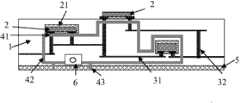
图1和图2分别为本发明的强化散热三维封装结构的一个实施例的立体示意图和剖面图。如图1和图2所示,本发明的强化散热三维封装结构包括:多层基板1、在基板上的器件2和连接器件的互连电路3、微通道4、散热板5、外部散热装置和水泵6;其中,微通道4包括在每一层基板上的水平方向的沟槽41以及各层基板之间的垂直方向的位置相对应的过孔42,形成互连的通道;散热板5设置在多层基板1的底部;散热板5与外部散热装置相连接;基板1的底部设有水泵的接口43,微通道4的端口通过接口43连接水泵。FIG. 1 and FIG. 2 are respectively a schematic perspective view and a cross-sectional view of an embodiment of a three-dimensional packaging structure with enhanced heat dissipation of the present invention. As shown in Fig. 1 and Fig. 2, the enhanced heat dissipation three-dimensional packaging structure of the present invention includes: a multilayer substrate 1, a
在本实施例中,水泵6采用内置微泵。互连电路3包括每一层基板2上的平面电路31和各层基板之间的垂直方向的通孔填料32,形成三维的互连电路。In this embodiment, the
本实施例的强化散热三维封装结构的封装方法,包括以下步骤The encapsulation method of the enhanced heat dissipation three-dimensional encapsulation structure of this embodiment includes the following steps
1)根据内置和表面的发热器件的需要,设计互连电路、无源器件和有源器件的位置;1) According to the needs of built-in and surface heating devices, design the positions of interconnection circuits, passive devices and active devices;
2)根据发热器件的尺寸和功率,设计微通道的形状、尺寸和分布,微通道的任意两条水平的沟槽或垂直的过孔的水平间距要超过单层的基板的厚度,大功率发热器件采用增加微通道的截面尺寸和分布密度的方法,微通道避开内置发热器件外接引线的位置,环绕分布在芯片周围,微通道与器件之间的距离为0~10倍单层基板厚度;2) According to the size and power of the heating device, design the shape, size and distribution of the microchannel. The horizontal distance between any two horizontal grooves or vertical via holes in the microchannel should exceed the thickness of a single-layer substrate. High-power heating The device adopts the method of increasing the cross-sectional size and distribution density of the microchannel. The microchannel avoids the position of the external lead wire of the built-in heating device, and is distributed around the chip. The distance between the microchannel and the device is 0 to 10 times the thickness of the single-layer substrate;
3)基板的底部设计内置微泵的位置;3) Design the position of the built-in micropump at the bottom of the substrate;
4)采用机械钻孔、冲孔、激光打孔或刻蚀的方法,在每一层的基板上制作互连电路的通孔、器件的空腔以及微通道的沟槽和过孔;4) Through mechanical drilling, punching, laser drilling or etching, through-holes for interconnection circuits, cavities for devices, and grooves and vias for microchannels are made on the substrate of each layer;
5)在每一层的基板上印刷Cu、Ag、Au等金属良导体作为平面电路和通孔填料,形成三维的互连电路,并采用较宽的布线宽度,布线的宽度为0.2~10mm,布线的间距不小于0.1mm;5) Print Cu, Ag, Au and other metal good conductors on the substrate of each layer as planar circuits and via hole fillers to form a three-dimensional interconnection circuit, and adopt a wider wiring width, the width of the wiring is 0.2-10mm, The wiring spacing is not less than 0.1mm;
6)通过金属焊料焊接或钎焊固定无源器件和有源器件,在内置的发热器件的四周涂敷一层导热绝缘胶21,表面的发热器件的底部涂覆一层导热绝缘胶,导热绝缘胶厚度为0~1mm,器件粘贴在基板的空腔内,将器件的引线与基板的互连焊接在一起,固定和连接水泵;6) Fix passive components and active components by metal solder welding or brazing, coat a layer of heat-conducting insulating
7)在预制的微通道的沟槽和过孔,以及空腔中填充石蜡等材料作为牺牲层材料,采用分层预压的方式,将多层预压好的基板采用定位孔或图像识别定位的方法使多层基板材料精确叠层对位;7) Fill the grooves, vias and cavities of the prefabricated microchannels with paraffin and other materials as sacrificial layer materials, and use layered pre-pressing methods to position the multi-layer pre-pressed substrates using positioning holes or image recognition The method makes the multi-layer substrate material laminated and aligned accurately;
8)针对不同的基板材料,分别采用PCB多层印刷电路板、厚膜陶瓷、低温共烧陶瓷、高温共烧陶瓷、金属沉积膜等基板封装技术,制造内嵌冷却微通道的封装基板,各层基板之间的平面电路通过通孔填料相连;8) For different substrate materials, PCB multilayer printed circuit boards, thick film ceramics, low-temperature co-fired ceramics, high-temperature co-fired ceramics, metal deposition films and other substrate packaging technologies are used to manufacture packaging substrates with embedded cooling microchannels. Planar circuits between layer substrates are connected by via filling;
9)基板底部焊接、粘接、溅射或沉积肋片型散热金属板,可以采用外接肋片空气自然冷却、风扇强制对流换热、外接冷却热管或外接水冷装置进行散热。9) Welding, bonding, sputtering or depositing finned heat dissipation metal plates on the bottom of the substrate can use external fins for natural air cooling, fan forced convection heat exchange, external cooling heat pipes or external water cooling devices for heat dissipation.
最后需要注意的是,公布实施方式的目的在于帮助进一步理解本发明,但是本领域的技术人员可以理解:在不脱离本发明及所附的权利要求的精神和范围内,各种替换和修改都是可能的。因此,本发明不应局限于实施例所公开的内容,本发明要求保护的范围以权利要求书界定的范围为准。Finally, it should be noted that the purpose of publishing the implementation is to help further understand the present invention, but those skilled in the art can understand that various replacements and modifications can be made without departing from the spirit and scope of the present invention and the appended claims. It is possible. Therefore, the present invention should not be limited to the content disclosed in the embodiments, and the protection scope of the present invention is subject to the scope defined in the claims.
Claims (10)
Priority Applications (1)
| Application Number | Priority Date | Filing Date | Title |
|---|---|---|---|
| CN201310481621.1ACN103489838B (en) | 2013-10-15 | 2013-10-15 | A kind of enhance heat three-dimension packaging structure and method for packing thereof |
Applications Claiming Priority (1)
| Application Number | Priority Date | Filing Date | Title |
|---|---|---|---|
| CN201310481621.1ACN103489838B (en) | 2013-10-15 | 2013-10-15 | A kind of enhance heat three-dimension packaging structure and method for packing thereof |
Publications (2)
| Publication Number | Publication Date |
|---|---|
| CN103489838Atrue CN103489838A (en) | 2014-01-01 |
| CN103489838B CN103489838B (en) | 2016-04-06 |
Family
ID=49829966
Family Applications (1)
| Application Number | Title | Priority Date | Filing Date |
|---|---|---|---|
| CN201310481621.1AExpired - Fee RelatedCN103489838B (en) | 2013-10-15 | 2013-10-15 | A kind of enhance heat three-dimension packaging structure and method for packing thereof |
Country Status (1)
| Country | Link |
|---|---|
| CN (1) | CN103489838B (en) |
Cited By (21)
| Publication number | Priority date | Publication date | Assignee | Title |
|---|---|---|---|---|
| CN103990501A (en)* | 2014-06-18 | 2014-08-20 | 云南师范大学 | Efficient heat-transmission and heat-isolation micro thermal control chip system |
| CN104959172A (en)* | 2015-05-22 | 2015-10-07 | 北京联合大学 | Microcirculation concept-based active heat dissipating three-dimensional chip |
| CN105188260A (en)* | 2015-11-02 | 2015-12-23 | 中国电子科技集团公司第二十六研究所 | Printed circuit board embedded runner liquid cooling heat exchange device |
| CN105540529A (en)* | 2015-12-04 | 2016-05-04 | 南通富士通微电子股份有限公司 | Adaptive temperature control chip microsystem |
| CN106256063A (en)* | 2014-05-14 | 2016-12-21 | 株式会社自动网络技术研究所 | circuit structure and electric connection box |
| CN107063232A (en)* | 2016-12-23 | 2017-08-18 | 中国电子科技集团公司信息科学研究院 | The navigator fix time service microdevice and its integrated approach of High Density Integration |
| CN107170726A (en)* | 2016-03-08 | 2017-09-15 | 丰田自动车工程及制造北美公司 | Power electronics component and semiconductor devices lamination |
| CN107734840A (en)* | 2017-11-29 | 2018-02-23 | 中国电子科技集团公司第二十六研究所 | Based on the cold cooling structure of printed circuit board three-dimensional micro-channel array liquid |
| CN107742621A (en)* | 2017-11-14 | 2018-02-27 | 桂林电子科技大学 | A heat dissipation device for embedded BGA packaging chips |
| CN109686708A (en)* | 2018-12-24 | 2019-04-26 | 中国电子科技集团公司第五十八研究所 | A kind of air-tightness and the radiator structure of non-airtight encapsulation |
| CN110139539A (en)* | 2019-05-27 | 2019-08-16 | 天津大学 | It is a kind of for microwave from the self assembly microchannel structural design and implementation method of package platforms |
| CN110354468A (en)* | 2019-07-12 | 2019-10-22 | 曹祖峰 | A kind of multichip IC encapsulation |
| CN110690645A (en)* | 2019-10-17 | 2020-01-14 | 中国科学院半导体研究所 | Laser array driving device and packaging method thereof |
| CN111584448A (en)* | 2020-05-19 | 2020-08-25 | 上海先方半导体有限公司 | Chip embedded micro-channel module packaging structure and manufacturing method |
| CN111725079A (en)* | 2020-05-18 | 2020-09-29 | 杨再西 | A high thermal conductivity plastic encapsulation process for leaded plastic encapsulated chips |
| CN113056087A (en)* | 2021-01-28 | 2021-06-29 | 中国电子科技集团公司第二十九研究所 | Printed circuit board embedded with micro-channel and preparation method thereof |
| CN113299618A (en)* | 2021-04-29 | 2021-08-24 | 中国电子科技集团公司第二十九研究所 | Three-dimensional integrated efficient heat dissipation packaging structure and preparation method thereof |
| CN113316370A (en)* | 2021-06-03 | 2021-08-27 | 苏州汇川联合动力系统有限公司 | Heat exchange assembly, heat dissipation structure and motor controller |
| CN114068599A (en)* | 2021-11-16 | 2022-02-18 | 苏州亚博汉智能科技有限公司 | 3d packaging method of chip |
| CN114727484A (en)* | 2022-03-16 | 2022-07-08 | 广东汇芯半导体有限公司 | Hexagonal semiconductor circuit and manufacturing method thereof |
| CN115172291A (en)* | 2022-07-27 | 2022-10-11 | 石家庄烽瓷电子技术有限公司 | HTCC structure with micro-channels |
Families Citing this family (1)
| Publication number | Priority date | Publication date | Assignee | Title |
|---|---|---|---|---|
| CN114334854A (en) | 2020-09-30 | 2022-04-12 | 华为技术有限公司 | Chip, method for manufacturing the same, and electronic device |
Citations (4)
| Publication number | Priority date | Publication date | Assignee | Title |
|---|---|---|---|---|
| US20040130874A1 (en)* | 2003-01-06 | 2004-07-08 | Maveety James G. | Embedded liquid pump and microchannel cooling system |
| CN1819165A (en)* | 2004-11-24 | 2006-08-16 | 朗迅科技公司 | Techniques for microchannel cooling |
| CN102148207A (en)* | 2009-11-06 | 2011-08-10 | 英特尔公司 | Direct liquid-contact micro-channel heat transfer devices, methods of temperature control for semiconductive devices, and processes of forming same |
| CN102769002A (en)* | 2011-04-30 | 2012-11-07 | 中国科学院微电子研究所 | Semiconductor device, forming method thereof and packaging structure |
- 2013
- 2013-10-15CNCN201310481621.1Apatent/CN103489838B/ennot_activeExpired - Fee Related
Patent Citations (4)
| Publication number | Priority date | Publication date | Assignee | Title |
|---|---|---|---|---|
| US20040130874A1 (en)* | 2003-01-06 | 2004-07-08 | Maveety James G. | Embedded liquid pump and microchannel cooling system |
| CN1819165A (en)* | 2004-11-24 | 2006-08-16 | 朗迅科技公司 | Techniques for microchannel cooling |
| CN102148207A (en)* | 2009-11-06 | 2011-08-10 | 英特尔公司 | Direct liquid-contact micro-channel heat transfer devices, methods of temperature control for semiconductive devices, and processes of forming same |
| CN102769002A (en)* | 2011-04-30 | 2012-11-07 | 中国科学院微电子研究所 | Semiconductor device, forming method thereof and packaging structure |
Cited By (31)
| Publication number | Priority date | Publication date | Assignee | Title |
|---|---|---|---|---|
| CN106256063B (en)* | 2014-05-14 | 2018-11-09 | 株式会社自动网络技术研究所 | circuit structure and electric connection box |
| CN106256063A (en)* | 2014-05-14 | 2016-12-21 | 株式会社自动网络技术研究所 | circuit structure and electric connection box |
| CN103990501A (en)* | 2014-06-18 | 2014-08-20 | 云南师范大学 | Efficient heat-transmission and heat-isolation micro thermal control chip system |
| CN104959172A (en)* | 2015-05-22 | 2015-10-07 | 北京联合大学 | Microcirculation concept-based active heat dissipating three-dimensional chip |
| CN105188260A (en)* | 2015-11-02 | 2015-12-23 | 中国电子科技集团公司第二十六研究所 | Printed circuit board embedded runner liquid cooling heat exchange device |
| CN105540529B (en)* | 2015-12-04 | 2017-11-10 | 通富微电子股份有限公司 | Adaptive Temperature Controlling Chip micro-system |
| CN105540529A (en)* | 2015-12-04 | 2016-05-04 | 南通富士通微电子股份有限公司 | Adaptive temperature control chip microsystem |
| CN107170726A (en)* | 2016-03-08 | 2017-09-15 | 丰田自动车工程及制造北美公司 | Power electronics component and semiconductor devices lamination |
| CN107170725A (en)* | 2016-03-08 | 2017-09-15 | 丰田自动车工程及制造北美公司 | The method of power electronics component and manufacture power electronics component |
| CN107170725B (en)* | 2016-03-08 | 2021-08-13 | 丰田自动车工程及制造北美公司 | Power electronic assembly and method of manufacturing power electronic assembly |
| CN107170726B (en)* | 2016-03-08 | 2021-03-12 | 丰田自动车工程及制造北美公司 | Power electronic components and semiconductor device stacks |
| CN107063232A (en)* | 2016-12-23 | 2017-08-18 | 中国电子科技集团公司信息科学研究院 | The navigator fix time service microdevice and its integrated approach of High Density Integration |
| CN107742621A (en)* | 2017-11-14 | 2018-02-27 | 桂林电子科技大学 | A heat dissipation device for embedded BGA packaging chips |
| CN107734840A (en)* | 2017-11-29 | 2018-02-23 | 中国电子科技集团公司第二十六研究所 | Based on the cold cooling structure of printed circuit board three-dimensional micro-channel array liquid |
| CN107734840B (en)* | 2017-11-29 | 2023-08-18 | 中国电子科技集团公司第二十六研究所 | Liquid-cooled cooling structure based on printed circuit board three-dimensional microchannel array |
| CN109686708A (en)* | 2018-12-24 | 2019-04-26 | 中国电子科技集团公司第五十八研究所 | A kind of air-tightness and the radiator structure of non-airtight encapsulation |
| CN110139539B (en)* | 2019-05-27 | 2021-01-05 | 天津大学 | A self-assembled microchannel design and implementation method for microwave self-encapsulation platform |
| CN110139539A (en)* | 2019-05-27 | 2019-08-16 | 天津大学 | It is a kind of for microwave from the self assembly microchannel structural design and implementation method of package platforms |
| CN110354468A (en)* | 2019-07-12 | 2019-10-22 | 曹祖峰 | A kind of multichip IC encapsulation |
| CN110690645B (en)* | 2019-10-17 | 2020-12-15 | 中国科学院半导体研究所 | Laser array driving device and packaging method thereof |
| CN110690645A (en)* | 2019-10-17 | 2020-01-14 | 中国科学院半导体研究所 | Laser array driving device and packaging method thereof |
| CN111725079A (en)* | 2020-05-18 | 2020-09-29 | 杨再西 | A high thermal conductivity plastic encapsulation process for leaded plastic encapsulated chips |
| CN111584448A (en)* | 2020-05-19 | 2020-08-25 | 上海先方半导体有限公司 | Chip embedded micro-channel module packaging structure and manufacturing method |
| CN113056087A (en)* | 2021-01-28 | 2021-06-29 | 中国电子科技集团公司第二十九研究所 | Printed circuit board embedded with micro-channel and preparation method thereof |
| CN113299618A (en)* | 2021-04-29 | 2021-08-24 | 中国电子科技集团公司第二十九研究所 | Three-dimensional integrated efficient heat dissipation packaging structure and preparation method thereof |
| CN113299618B (en)* | 2021-04-29 | 2023-07-14 | 中国电子科技集团公司第二十九研究所 | A three-dimensional integrated high-efficiency heat dissipation packaging structure and its preparation method |
| CN113316370A (en)* | 2021-06-03 | 2021-08-27 | 苏州汇川联合动力系统有限公司 | Heat exchange assembly, heat dissipation structure and motor controller |
| WO2022253241A1 (en)* | 2021-06-03 | 2022-12-08 | 苏州汇川联合动力系统有限公司 | Heat exchange assembly, heat dissipation structure, and electric motor controller |
| CN114068599A (en)* | 2021-11-16 | 2022-02-18 | 苏州亚博汉智能科技有限公司 | 3d packaging method of chip |
| CN114727484A (en)* | 2022-03-16 | 2022-07-08 | 广东汇芯半导体有限公司 | Hexagonal semiconductor circuit and manufacturing method thereof |
| CN115172291A (en)* | 2022-07-27 | 2022-10-11 | 石家庄烽瓷电子技术有限公司 | HTCC structure with micro-channels |
Also Published As
| Publication number | Publication date |
|---|---|
| CN103489838B (en) | 2016-04-06 |
Similar Documents
| Publication | Publication Date | Title |
|---|---|---|
| CN103489838B (en) | A kind of enhance heat three-dimension packaging structure and method for packing thereof | |
| CN105188260B (en) | Printed circuit board embeds runner liquid cooling heat-exchanger rig | |
| CN101826494B (en) | Heat dissipation device and preparation method based on carbon nanotube array and low temperature co-fired ceramics | |
| CN109524373A (en) | The three-dimensional active heat removal encapsulating structure and its manufacture craft of embedded fluid channel | |
| US20100187682A1 (en) | Electronic package and method of assembling the same | |
| CN105611801B (en) | Fluid channel radiator structure and method | |
| WO2020248905A1 (en) | Wafer-level 3d stacked microchannel heat dissipation structure and manufacturing method therefor | |
| CN104465552A (en) | Packaging structure and optical module | |
| CN204230225U (en) | Electronic device | |
| US20160095197A1 (en) | Circuit board module and circuit board structure | |
| CN113056087A (en) | Printed circuit board embedded with micro-channel and preparation method thereof | |
| CN104112736A (en) | 3D-IC with inter-layer complex microchannel fluid cooling function | |
| WO2022241846A1 (en) | Lead bonding structure comprising embedded manifold type micro-channel and preparation method for lead bonding structure | |
| CN114121850A (en) | Liquid-cooled micro-channel embedded ceramic packaging structure, ceramic packaging shell and preparation method | |
| WO2016071324A1 (en) | Hermetically sealed heat pipe structure synthesized with support structure and method for producing it | |
| JP4997954B2 (en) | Circuit board, manufacturing method thereof, and semiconductor device | |
| CN113363164A (en) | Square chip packaging method and packaging structure thereof | |
| CN105374771A (en) | Power semiconductor module and method for cooling power semiconductor module | |
| CN118553701B (en) | Micro-channel liquid cooling integrated packaging structure of embedded power module | |
| CN105990275B (en) | Power module package part and preparation method thereof | |
| CN114005803A (en) | Integrated embedded micro-channel heat dissipation system and method of micro-system | |
| CN205069617U (en) | Power module and vehicle that has it | |
| CN209418488U (en) | A Metal Microchannel Heat Sink Structure for Chip Heat Dissipation | |
| JP2013131680A (en) | Electronic apparatus and manufacturing method of the same | |
| CN116093043A (en) | A microchannel cooling device with a columnar embedded module |
Legal Events
| Date | Code | Title | Description |
|---|---|---|---|
| C06 | Publication | ||
| PB01 | Publication | ||
| C10 | Entry into substantive examination | ||
| SE01 | Entry into force of request for substantive examination | ||
| C14 | Grant of patent or utility model | ||
| GR01 | Patent grant | ||
| CF01 | Termination of patent right due to non-payment of annual fee | ||
| CF01 | Termination of patent right due to non-payment of annual fee | Granted publication date:20160406 Termination date:20191015 |