CN103487160A - Method for manufacturing Pt resistor temperature sensor - Google Patents
Method for manufacturing Pt resistor temperature sensorDownload PDFInfo
- Publication number
- CN103487160A CN103487160ACN201310451756.3ACN201310451756ACN103487160ACN 103487160 ACN103487160 ACN 103487160ACN 201310451756 ACN201310451756 ACN 201310451756ACN 103487160 ACN103487160 ACN 103487160A
- Authority
- CN
- China
- Prior art keywords
- temperature sensor
- photoresist
- ceramic substrate
- metal
- resistance temperature
- Prior art date
- Legal status (The legal status is an assumption and is not a legal conclusion. Google has not performed a legal analysis and makes no representation as to the accuracy of the status listed.)
- Pending
Links
- 238000000034methodMethods0.000titleclaimsabstractdescription28
- 238000004519manufacturing processMethods0.000titleclaimsabstractdescription18
- 239000002184metalSubstances0.000claimsabstractdescription28
- 229910052751metalInorganic materials0.000claimsabstractdescription28
- 229920001486SU-8 photoresistPolymers0.000claimsabstractdescription26
- 239000000758substrateSubstances0.000claimsabstractdescription23
- 239000000919ceramicSubstances0.000claimsabstractdescription22
- 229920002120photoresistant polymerPolymers0.000claimsabstractdescription14
- 239000003292glueSubstances0.000claimsabstractdescription13
- 238000001755magnetron sputter depositionMethods0.000claimsabstractdescription10
- 150000003839saltsChemical class0.000claimsabstractdescription6
- 239000012298atmosphereSubstances0.000claimsabstractdescription3
- 238000001259photo etchingMethods0.000claimsabstract2
- 238000002679ablationMethods0.000claimsdescription5
- 238000005516engineering processMethods0.000claimsdescription4
- 238000001459lithographyMethods0.000claimsdescription2
- 239000011248coating agentSubstances0.000abstract1
- 238000000576coating methodMethods0.000abstract1
- BASFCYQUMIYNBI-UHFFFAOYSA-NplatinumSubstances[Pt]BASFCYQUMIYNBI-UHFFFAOYSA-N0.000description27
- XLYOFNOQVPJJNP-UHFFFAOYSA-NwaterChemical compoundOXLYOFNOQVPJJNP-UHFFFAOYSA-N0.000description4
- 238000005530etchingMethods0.000description3
- 238000010884ion-beam techniqueMethods0.000description3
- 239000007822coupling agentSubstances0.000description2
- 239000008367deionised waterSubstances0.000description2
- 229910021641deionized waterInorganic materials0.000description2
- FFUAGWLWBBFQJT-UHFFFAOYSA-NhexamethyldisilazaneChemical compoundC[Si](C)(C)N[Si](C)(C)CFFUAGWLWBBFQJT-UHFFFAOYSA-N0.000description2
- 238000000206photolithographyMethods0.000description2
- 238000004544sputter depositionMethods0.000description2
- LFQSCWFLJHTTHZ-UHFFFAOYSA-NEthanolChemical compoundCCOLFQSCWFLJHTTHZ-UHFFFAOYSA-N0.000description1
- HEMHJVSKTPXQMS-UHFFFAOYSA-MSodium hydroxideChemical class[OH-].[Na+]HEMHJVSKTPXQMS-UHFFFAOYSA-M0.000description1
- 230000007812deficiencyEffects0.000description1
- 238000000151depositionMethods0.000description1
- 230000008021depositionEffects0.000description1
- 230000000694effectsEffects0.000description1
- 238000005566electron beam evaporationMethods0.000description1
- 238000004377microelectronicMethods0.000description1
- 229910052697platinumInorganic materials0.000description1
- 238000002360preparation methodMethods0.000description1
- 239000002904solventSubstances0.000description1
- 238000004528spin coatingMethods0.000description1
- 238000005507sprayingMethods0.000description1
Images
Landscapes
- Thermistors And Varistors (AREA)
Abstract
Translated fromChineseDescription
Translated fromChinese技术领域technical field
本发明涉及传感器制造技术,尤其是涉及一种Pt电阻温度传感器的制造方法。The invention relates to sensor manufacturing technology, in particular to a manufacturing method of a Pt resistance temperature sensor.
背景技术Background technique
Pt金属由于其优异的温度特性特别适合于制造温度传感器。当前制造Pt电阻温度传感器的方法主要是采用磁控溅射法得到Pt金属薄膜,然后在Pt金属薄膜上涂胶、光刻,再以光刻胶作为掩模用离子束刻蚀的办法刻蚀出Pt金属微结构图形。通常Pt金属的厚度在2μm左右,而目前的工艺方法存在的问题是离子束刻蚀速率很慢,刻蚀2μm厚的Pt金属需要3~4个小时,这使制备效率和加工成本难以降低。Pt metal is particularly suitable for manufacturing temperature sensors due to its excellent temperature characteristics. The current method of manufacturing Pt resistance temperature sensor is mainly to use magnetron sputtering method to obtain Pt metal film, then apply glue on the Pt metal film, photolithography, and then use photoresist as a mask to etch with ion beam etching Figure out the microstructure pattern of Pt metal. Usually, the thickness of Pt metal is about 2 μm, but the problem with the current process is that the ion beam etching rate is very slow, and it takes 3 to 4 hours to etch Pt metal with a thickness of 2 μm, which makes it difficult to reduce the production efficiency and processing cost.
发明内容Contents of the invention
为了克服上述现有技术的不足,本发明提出了一种Pt电阻温度传感器的制造方法。In order to overcome the deficiencies of the prior art above, the present invention proposes a method for manufacturing a Pt resistance temperature sensor.
本发明采用如下技术方案:The present invention adopts following technical scheme:
一种Pt电阻温度传感器的制造方法,包括以下步骤:A method for manufacturing a Pt resistance temperature sensor, comprising the following steps:
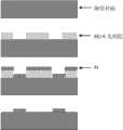
第一步,在陶瓷衬底上涂覆SU-8光刻胶,光刻出微结构图形;The first step is to coat SU-8 photoresist on the ceramic substrate, and photolithographically produce microstructure patterns;
第二步,将光刻完成的陶瓷基片放入磁控溅射设备,沉积Pt金属薄膜;The second step is to put the photolithographically completed ceramic substrate into the magnetron sputtering equipment to deposit Pt metal film;
第三步,将上述得到的SU-8光刻胶上带有Pt金属的陶瓷基片放到O2气氛中的炉子中烧蚀或者在盐浴中将SU-8胶去除,最后得到沉积在陶瓷衬底上的Pt金属微结构图形。In the third step, put the ceramic substrate with Pt metal on the SU-8 photoresist obtained above intoO2 for ablation in a furnace in an atmosphere or remove the SU-8 glue in a salt bath, and finally obtain the deposited on Pt metal microstructure patterns on ceramic substrates.
本技术方案中,沉积Pt金属的厚度是2μm左右。SU-8光刻胶是一种负性光刻胶,具有耐热性好,可以承受在磁控溅射过程中产生的热量而不会发生结构变形。在剥离工艺中,为避免金属薄膜在微结构侧壁边缘的连续,光刻胶的厚度应该是金属层厚度的2~3倍以上。SU-8光刻胶是一种负性光刻胶,厚度很容易控制在5~10μm。磁控溅射工艺的采用可以提高Pt金属和陶瓷基片的结合力。在SU-8胶上溅射Pt金属完成后,用烧蚀的方法或者盐浴的方法,很容易完成SU-8胶的去除。In this technical solution, the thickness of deposited Pt metal is about 2 μm. SU-8 photoresist is a negative photoresist with good heat resistance and can withstand the heat generated during magnetron sputtering without structural deformation. In the lift-off process, in order to avoid the continuity of the metal film at the edge of the sidewall of the microstructure, the thickness of the photoresist should be more than 2 to 3 times the thickness of the metal layer. SU-8 photoresist is a negative photoresist whose thickness can be easily controlled within 5-10μm. The use of magnetron sputtering technology can improve the bonding force between Pt metal and ceramic substrate. After sputtering Pt metal on the SU-8 glue, it is easy to remove the SU-8 glue by ablation method or salt bath method.
本发明获得如下效果:The present invention obtains following effect:
1.SU-8胶作为剥离工艺首次在Pt电阻温度传感器制造工艺中被提出。SU-8胶在曝光,后烘完成后是交联状的网状结构,因此在较高温度下不易分解,能够耐住在磁控溅射工艺中产生的热量而不会变形。1. SU-8 glue was first proposed as a stripping process in the manufacturing process of Pt resistance temperature sensor. SU-8 glue has a cross-linked network structure after exposure and post-baking, so it is not easy to decompose at higher temperatures, and can withstand the heat generated in the magnetron sputtering process without deformation.
2.为了使溅射的Pt金属薄膜不连续,SU-8光刻胶的厚度要是Pt金属薄膜厚度2~3倍。2. In order to make the sputtered Pt metal film discontinuous, the thickness of the SU-8 photoresist should be 2 to 3 times the thickness of the Pt metal film.
3.Pt金属薄膜的沉积要用磁控溅射设备完成,这是因为磁控溅射工艺金属在衬底上的附著力更大,在去除SU-8胶的过程中不易脱落。3. The deposition of the Pt metal film should be completed by magnetron sputtering equipment, because the magnetron sputtering process metal has a stronger adhesion on the substrate, and it is not easy to fall off during the process of removing the SU-8 glue.
4.SU-8光刻胶可以采用高温烧蚀或者盐浴的办法去除,这有别于微电子工艺中常用的剥离工艺(在溶剂中完成)。4. SU-8 photoresist can be removed by high temperature ablation or salt bath, which is different from the stripping process (completed in solvent) commonly used in microelectronics technology.
5.采用此制备方法,不会用到离子束刻蚀工艺这一瓶颈工艺,减少了设备投资,而且更重要的是工艺大大简化,大大减少了流片时间。5. With this preparation method, the bottleneck process of ion beam etching process will not be used, which reduces equipment investment, and more importantly, the process is greatly simplified and the tape-out time is greatly reduced.
附图说明Description of drawings
图为铂电阻温度传感器的制造工艺流程图。The figure shows the manufacturing process flow chart of the platinum resistance temperature sensor.
具体实施方式Detailed ways
实施例1Example 1
一种Pt电阻温度传感器的制造方法,包括以下步骤:A method for manufacturing a Pt resistance temperature sensor, comprising the following steps:
(1)将一定尺寸的陶瓷基片(比如3寸)用无水乙醇(MOS级)、去离子水依次清洗,然后烘干,然后在陶瓷基片上蒸发HMDS(一种偶联剂)。(1) Clean a ceramic substrate of a certain size (such as 3 inches) with absolute ethanol (MOS grade) and deionized water in sequence, then dry it, and then evaporate HMDS (a coupling agent) on the ceramic substrate.
(2)用旋转涂胶的办法将SU-82025(SU-8胶的一种型号)光刻胶涂覆到处理好的陶瓷基片上,厚度5μm~10μm。(2) Apply SU-82025 (a type of SU-8 glue) photoresist to the processed ceramic substrate by spin coating method, with a thickness of 5 μm to 10 μm.
(3)在热板上对光刻胶进行前烘,条件是65℃/3min,95℃/5min。(3) Pre-bake the photoresist on a hot plate under the conditions of 65°C/3min and 95°C/5min.
(4)在紫外光源的光刻机进行曝光,曝光计量为150mJ/cm2。(4) Expose in a lithography machine with an ultraviolet light source, and the exposure meter is 150 mJ/cm2 .
(5)在热板上进行后烘,条件为65℃/1min,95℃/5min。(5) After-baking on a hot plate, the conditions are 65°C/1min, 95°C/5min.
(6)用SU-8专用显影液进行显影,并用O2等离子体去底膜。(6) Develop with SU-8 special developer, and useO2 plasma to remove the bottom film.
(7)将光刻完成的陶瓷基片放入磁控多靶溅射机上沉积Pt金属,厚度在2μm左右。(7) Put the photolithographically completed ceramic substrate into a magnetron multi-target sputtering machine to deposit Pt metal with a thickness of about 2 μm.
(8)将溅射完成的陶瓷基片高温烧蚀,去除SU-8光刻胶及附着在光刻胶上的Pt金属。(8) The sputtered ceramic substrate is ablated at high temperature to remove the SU-8 photoresist and the Pt metal attached to the photoresist.
(9)用离子水清洗,烘干。(9) Wash with ionized water and dry.
实施例2Example 2
(1)将一定尺寸的陶瓷基片(比如3寸)用H2SO4+H2O2、去离子水依次清洗,然后烘干,然后在陶瓷基片上蒸发HMDS(一种偶联剂)。(1) Wash a ceramic substrate of a certain size (such as 3 inches) with H2 SO4 +H2 O2 and deionized water in sequence, then dry it, and then evaporate HMDS (a coupling agent) on the ceramic substrate .
(2)用喷胶工艺的办法将SU-82025(SU-8胶的一种型号)光刻胶涂覆到处理好的陶瓷基片上,厚度5μm~10μm。(2) Apply SU-82025 (a type of SU-8 glue) photoresist to the processed ceramic substrate by spraying glue, with a thickness of 5 μm to 10 μm.
(3)在热板上对光刻胶进行前烘,条件是65℃/3min,95℃/5min。(3) Pre-bake the photoresist on a hot plate under the conditions of 65°C/3min and 95°C/5min.
(4)在紫外光源的光刻机进行曝光,曝光计量为150mJ/cm2。(4) Expose in a photolithography machine with an ultraviolet light source, and the exposure meter is 150 mJ/cm2 .
(5)在热板上进行后烘,条件为65℃/1min,95℃/5min。(5) After-baking on a hot plate, the conditions are 65°C/1min, 95°C/5min.
(6)用SU-8专用显影液进行显影,并用O2等离子体去底膜。(6) Develop with SU-8 special developer, and useO2 plasma to remove the bottom film.
(7)将电子束蒸发设备在上述得到陶瓷基片Pt金属,厚度在2μm左右。(7) Put the electron beam evaporation equipment above to obtain the ceramic substrate Pt metal with a thickness of about 2 μm.
(8)将上述得到的陶瓷基片放入NaOH盐浴炉中高温去除SU-8光刻胶及附着在光刻胶上的Pt金属。(8) Put the ceramic substrate obtained above into a NaOH salt bath furnace at high temperature to remove the SU-8 photoresist and the Pt metal attached to the photoresist.
(9)用离子水清洗,烘干。(9) Wash with ionized water and dry.
Claims (6)
Priority Applications (1)
| Application Number | Priority Date | Filing Date | Title |
|---|---|---|---|
| CN201310451756.3ACN103487160A (en) | 2013-09-27 | 2013-09-27 | Method for manufacturing Pt resistor temperature sensor |
Applications Claiming Priority (1)
| Application Number | Priority Date | Filing Date | Title |
|---|---|---|---|
| CN201310451756.3ACN103487160A (en) | 2013-09-27 | 2013-09-27 | Method for manufacturing Pt resistor temperature sensor |
Publications (1)
| Publication Number | Publication Date |
|---|---|
| CN103487160Atrue CN103487160A (en) | 2014-01-01 |
Family
ID=49827561
Family Applications (1)
| Application Number | Title | Priority Date | Filing Date |
|---|---|---|---|
| CN201310451756.3APendingCN103487160A (en) | 2013-09-27 | 2013-09-27 | Method for manufacturing Pt resistor temperature sensor |
Country Status (1)
| Country | Link |
|---|---|
| CN (1) | CN103487160A (en) |
Cited By (5)
| Publication number | Priority date | Publication date | Assignee | Title |
|---|---|---|---|---|
| CN104317173A (en)* | 2014-11-14 | 2015-01-28 | 四川飞阳科技有限公司 | Method for increasing yield of stripping technology |
| CN106197718A (en)* | 2016-08-31 | 2016-12-07 | 北京埃德万斯离子束技术研究所股份有限公司 | A kind of film temperature sensor and preparation method |
| CN111351607A (en)* | 2019-11-13 | 2020-06-30 | 中国科学院微电子研究所 | Manufacturing method of temperature and pressure composite sensor |
| CN111397776A (en)* | 2019-11-13 | 2020-07-10 | 中国科学院微电子研究所 | Temperature and pressure composite sensor |
| CN114460819A (en)* | 2022-01-14 | 2022-05-10 | 北京量子信息科学研究院 | Alignment mark for electron beam exposure and preparation method thereof |
Citations (6)
| Publication number | Priority date | Publication date | Assignee | Title |
|---|---|---|---|---|
| US4050052A (en)* | 1975-06-21 | 1977-09-20 | W. C. Heraeus Gmbh | Electrical temperature measuring resistor structure, particularly for resistance thermometers |
| CN1042793A (en)* | 1988-11-16 | 1990-06-06 | 中国科学院上海冶金研究所 | Platinum thin film manufacturing method for temperature sensor |
| JPH04265828A (en)* | 1991-02-20 | 1992-09-22 | Murata Mfg Co Ltd | Platinum temperature sensor |
| CN102496431A (en)* | 2011-12-12 | 2012-06-13 | 中国振华集团云科电子有限公司 | Manufacturing method of platinum film resistor chip for temperature sensor |
| CN103017922A (en)* | 2011-09-26 | 2013-04-03 | 中国电子科技集团公司第四十八研究所 | Quick-response film-thermocouple temperature sensor and manufacturing method thereof |
| CN103021605A (en)* | 2012-12-19 | 2013-04-03 | 中国振华集团云科电子有限公司 | Production method for chip type platinum thermosensitive resistors |
- 2013
- 2013-09-27CNCN201310451756.3Apatent/CN103487160A/enactivePending
Patent Citations (6)
| Publication number | Priority date | Publication date | Assignee | Title |
|---|---|---|---|---|
| US4050052A (en)* | 1975-06-21 | 1977-09-20 | W. C. Heraeus Gmbh | Electrical temperature measuring resistor structure, particularly for resistance thermometers |
| CN1042793A (en)* | 1988-11-16 | 1990-06-06 | 中国科学院上海冶金研究所 | Platinum thin film manufacturing method for temperature sensor |
| JPH04265828A (en)* | 1991-02-20 | 1992-09-22 | Murata Mfg Co Ltd | Platinum temperature sensor |
| CN103017922A (en)* | 2011-09-26 | 2013-04-03 | 中国电子科技集团公司第四十八研究所 | Quick-response film-thermocouple temperature sensor and manufacturing method thereof |
| CN102496431A (en)* | 2011-12-12 | 2012-06-13 | 中国振华集团云科电子有限公司 | Manufacturing method of platinum film resistor chip for temperature sensor |
| CN103021605A (en)* | 2012-12-19 | 2013-04-03 | 中国振华集团云科电子有限公司 | Production method for chip type platinum thermosensitive resistors |
Non-Patent Citations (1)
| Title |
|---|
| 崔峰等: ""SU-8胶模去除技术"", 《微细加工技术》* |
Cited By (8)
| Publication number | Priority date | Publication date | Assignee | Title |
|---|---|---|---|---|
| CN104317173A (en)* | 2014-11-14 | 2015-01-28 | 四川飞阳科技有限公司 | Method for increasing yield of stripping technology |
| CN106197718A (en)* | 2016-08-31 | 2016-12-07 | 北京埃德万斯离子束技术研究所股份有限公司 | A kind of film temperature sensor and preparation method |
| CN106197718B (en)* | 2016-08-31 | 2019-08-27 | 北京埃德万斯离子束技术研究所股份有限公司 | A kind of film temperature sensor and preparation method |
| CN111351607A (en)* | 2019-11-13 | 2020-06-30 | 中国科学院微电子研究所 | Manufacturing method of temperature and pressure composite sensor |
| CN111397776A (en)* | 2019-11-13 | 2020-07-10 | 中国科学院微电子研究所 | Temperature and pressure composite sensor |
| CN111351607B (en)* | 2019-11-13 | 2022-01-11 | 中国科学院微电子研究所 | Manufacturing method of temperature and pressure composite sensor |
| CN114460819A (en)* | 2022-01-14 | 2022-05-10 | 北京量子信息科学研究院 | Alignment mark for electron beam exposure and preparation method thereof |
| CN114460819B (en)* | 2022-01-14 | 2024-01-26 | 北京量子信息科学研究院 | Alignment mark for electron beam exposure and preparation method thereof |
Similar Documents
| Publication | Publication Date | Title |
|---|---|---|
| CN103346094B (en) | A kind of lithographic method of microwave membrane circuit | |
| CN103715070B (en) | A kind of method with glue magnetron sputtering thick film | |
| CN103487160A (en) | Method for manufacturing Pt resistor temperature sensor | |
| CN100479102C (en) | Stripping preparation method of graphics platinum/titanium metal thin film | |
| CN101566799B (en) | Method for preparing hollowed-out polyimide evaporation mask stencil | |
| CN102556950B (en) | Tunable artificial electromagnetic material based on three-layer structure and manufacturing method thereof | |
| CN108511573A (en) | A kind of preparation method of GaN base light emitting chip | |
| CN103058126A (en) | Processing method for surface electrodes of three-dimensional quartz micro-mechanical structure | |
| CN115440585A (en) | Metal nanostructure and its ion beam etching processing method | |
| CN103151245A (en) | Thin film patterning method | |
| WO2017041485A1 (en) | Thin-film transistor, manufacturing method therefor and display panel | |
| CN108803261A (en) | Metal pattern processing method for convenient peeling of single-layer positive glue | |
| CN104934329B (en) | Preparation method for ZnO-Thin Film Transistor (ZnO-TFT) based on flexible substrate material | |
| CN105742191A (en) | Preparation method for molybdenum disulfide nanometer film with preset patterns | |
| CN113862770A (en) | Method for preparing patterned electrode by deplating process | |
| CN118588535A (en) | Photoresist stripping method | |
| CN113721421A (en) | Machining method of nano-imprinting structure | |
| CN102956759B (en) | Method for preparing ITO (indium tin oxide) patterns by stripping | |
| CN103996618B (en) | Manufacturing method for TFT electrode lead | |
| CN107785308B (en) | Method for preparing an array substrate and array substrate | |
| CN113816335A (en) | Metal stripping preparation method of silicon-based wafer double-layer photoresist | |
| CN103548173A (en) | Manufacturing equipment for the manufacture of layered structures | |
| WO2015000272A1 (en) | Signal substrate of naked eye 3d function panel, manufacturing method therefor and display device | |
| CN116054770B (en) | Method for preparing interdigital electrode by stripping process | |
| CN106444293A (en) | Preparation method of metal pattern |
Legal Events
| Date | Code | Title | Description |
|---|---|---|---|
| C06 | Publication | ||
| PB01 | Publication | ||
| C10 | Entry into substantive examination | ||
| SE01 | Entry into force of request for substantive examination | ||
| C02 | Deemed withdrawal of patent application after publication (patent law 2001) | ||
| WD01 | Invention patent application deemed withdrawn after publication | Application publication date:20140101 |