CN103474397A - Method of making a FINFET device - Google Patents
Method of making a FINFET deviceDownload PDFInfo
- Publication number
- CN103474397A CN103474397ACN201310035323XACN201310035323ACN103474397ACN 103474397 ACN103474397 ACN 103474397ACN 201310035323X ACN201310035323X ACN 201310035323XACN 201310035323 ACN201310035323 ACN 201310035323ACN 103474397 ACN103474397 ACN 103474397A
- Authority
- CN
- China
- Prior art keywords
- fin
- pseudo
- semiconductor substrate
- etching
- fins
- Prior art date
- Legal status (The legal status is an assumption and is not a legal conclusion. Google has not performed a legal analysis and makes no representation as to the accuracy of the status listed.)
- Granted
Links
- 238000004519manufacturing processMethods0.000titleclaimsabstractdescription12
- 239000004065semiconductorSubstances0.000claimsabstractdescription68
- 239000000758substrateSubstances0.000claimsabstractdescription61
- 238000000034methodMethods0.000claimsdescription134
- 238000005530etchingMethods0.000claimsdescription55
- 229920002120photoresistant polymerPolymers0.000claimsdescription39
- 238000002955isolationMethods0.000claimsdescription16
- 238000000059patterningMethods0.000claimsdescription14
- 239000002243precursorSubstances0.000claimsdescription10
- 230000015572biosynthetic processEffects0.000claimsdescription8
- 230000005669field effectEffects0.000claimsdescription7
- 239000010410layerSubstances0.000description97
- 230000008569processEffects0.000description58
- VYPSYNLAJGMNEJ-UHFFFAOYSA-NSilicium dioxideChemical compoundO=[Si]=OVYPSYNLAJGMNEJ-UHFFFAOYSA-N0.000description22
- 239000003989dielectric materialSubstances0.000description13
- 239000000463materialSubstances0.000description13
- 235000012239silicon dioxideNutrition0.000description11
- 239000000377silicon dioxideSubstances0.000description11
- 229910052581Si3N4Inorganic materials0.000description9
- XUIMIQQOPSSXEZ-UHFFFAOYSA-NSiliconChemical compound[Si]XUIMIQQOPSSXEZ-UHFFFAOYSA-N0.000description9
- 229910052710siliconInorganic materials0.000description9
- 239000010703siliconSubstances0.000description9
- HQVNEWCFYHHQES-UHFFFAOYSA-Nsilicon nitrideChemical compoundN12[Si]34N5[Si]62N3[Si]51N64HQVNEWCFYHHQES-UHFFFAOYSA-N0.000description9
- 239000007789gasSubstances0.000description8
- 238000001312dry etchingMethods0.000description7
- 125000006850spacer groupChemical group0.000description6
- RYGMFSIKBFXOCR-UHFFFAOYSA-NCopperChemical compound[Cu]RYGMFSIKBFXOCR-UHFFFAOYSA-N0.000description5
- 230000008901benefitEffects0.000description5
- 229910052802copperInorganic materials0.000description5
- 239000010949copperSubstances0.000description5
- 229910052751metalInorganic materials0.000description5
- 239000002184metalSubstances0.000description5
- WFKWXMTUELFFGS-UHFFFAOYSA-NtungstenChemical compound[W]WFKWXMTUELFFGS-UHFFFAOYSA-N0.000description5
- 229910052721tungstenInorganic materials0.000description5
- 239000010937tungstenSubstances0.000description5
- 229910000577Silicon-germaniumInorganic materials0.000description4
- 238000000137annealingMethods0.000description4
- 238000005229chemical vapour depositionMethods0.000description4
- 238000000151depositionMethods0.000description4
- 239000011229interlayerSubstances0.000description4
- 238000012545processingMethods0.000description4
- 238000001039wet etchingMethods0.000description4
- YCKRFDGAMUMZLT-UHFFFAOYSA-NFluorine atomChemical compound[F]YCKRFDGAMUMZLT-UHFFFAOYSA-N0.000description3
- LEVVHYCKPQWKOP-UHFFFAOYSA-N[Si].[Ge]Chemical compound[Si].[Ge]LEVVHYCKPQWKOP-UHFFFAOYSA-N0.000description3
- PNEYBMLMFCGWSK-UHFFFAOYSA-Naluminium oxideInorganic materials[O-2].[O-2].[O-2].[Al+3].[Al+3]PNEYBMLMFCGWSK-UHFFFAOYSA-N0.000description3
- 230000008021depositionEffects0.000description3
- 238000013461designMethods0.000description3
- 238000005516engineering processMethods0.000description3
- 229910052731fluorineInorganic materials0.000description3
- 239000011737fluorineSubstances0.000description3
- 229910044991metal oxideInorganic materials0.000description3
- 150000004706metal oxidesChemical class0.000description3
- 239000012071phaseSubstances0.000description3
- 238000005549size reductionMethods0.000description3
- 239000000126substanceSubstances0.000description3
- 206010010144Completed suicideDiseases0.000description2
- MCMNRKCIXSYSNV-UHFFFAOYSA-NZirconium dioxideChemical compoundO=[Zr]=OMCMNRKCIXSYSNV-UHFFFAOYSA-N0.000description2
- 238000013459approachMethods0.000description2
- 238000000231atomic layer depositionMethods0.000description2
- QVGXLLKOCUKJST-UHFFFAOYSA-Natomic oxygenChemical compound[O]QVGXLLKOCUKJST-UHFFFAOYSA-N0.000description2
- 239000000460chlorineSubstances0.000description2
- 239000004020conductorSubstances0.000description2
- 230000009977dual effectEffects0.000description2
- CJNBYAVZURUTKZ-UHFFFAOYSA-Nhafnium(IV) oxideInorganic materialsO=[Hf]=OCJNBYAVZURUTKZ-UHFFFAOYSA-N0.000description2
- 238000002513implantationMethods0.000description2
- 229910010272inorganic materialInorganic materials0.000description2
- 239000011147inorganic materialSubstances0.000description2
- 239000011368organic materialSubstances0.000description2
- 230000003647oxidationEffects0.000description2
- 238000007254oxidation reactionMethods0.000description2
- 239000001301oxygenSubstances0.000description2
- 229910052760oxygenInorganic materials0.000description2
- 238000005498polishingMethods0.000description2
- 238000004151rapid thermal annealingMethods0.000description2
- HBMJWWWQQXIZIP-UHFFFAOYSA-Nsilicon carbideChemical compound[Si+]#[C-]HBMJWWWQQXIZIP-UHFFFAOYSA-N0.000description2
- 229910010271silicon carbideInorganic materials0.000description2
- 238000000038ultrahigh vacuum chemical vapour depositionMethods0.000description2
- 238000000927vapour-phase epitaxyMethods0.000description2
- 239000011800void materialSubstances0.000description2
- ITWBWJFEJCHKSN-UHFFFAOYSA-N1,4,7-triazonaneChemical compoundC1CNCCNCCN1ITWBWJFEJCHKSN-UHFFFAOYSA-N0.000description1
- ZCYVEMRRCGMTRW-UHFFFAOYSA-N7553-56-2Chemical compound[I]ZCYVEMRRCGMTRW-UHFFFAOYSA-N0.000description1
- JBRZTFJDHDCESZ-UHFFFAOYSA-NAsGaChemical compound[As]#[Ga]JBRZTFJDHDCESZ-UHFFFAOYSA-N0.000description1
- WKBOTKDWSSQWDR-UHFFFAOYSA-NBromine atomChemical compound[Br]WKBOTKDWSSQWDR-UHFFFAOYSA-N0.000description1
- ZAMOUSCENKQFHK-UHFFFAOYSA-NChlorine atomChemical compound[Cl]ZAMOUSCENKQFHK-UHFFFAOYSA-N0.000description1
- 229910001218Gallium arsenideInorganic materials0.000description1
- 229910004129HfSiOInorganic materials0.000description1
- ZOKXTWBITQBERF-UHFFFAOYSA-NMolybdenumChemical compound[Mo]ZOKXTWBITQBERF-UHFFFAOYSA-N0.000description1
- 229910004200TaSiNInorganic materials0.000description1
- 229910010038TiAlInorganic materials0.000description1
- 229910010037TiAlNInorganic materials0.000description1
- ATJFFYVFTNAWJD-UHFFFAOYSA-NTinChemical compound[Sn]ATJFFYVFTNAWJD-UHFFFAOYSA-N0.000description1
- RTAQQCXQSZGOHL-UHFFFAOYSA-NTitaniumChemical compound[Ti]RTAQQCXQSZGOHL-UHFFFAOYSA-N0.000description1
- 229910045601alloyInorganic materials0.000description1
- 239000000956alloySubstances0.000description1
- 230000004075alterationEffects0.000description1
- 229910052782aluminiumInorganic materials0.000description1
- XAGFODPZIPBFFR-UHFFFAOYSA-NaluminiumChemical compound[Al]XAGFODPZIPBFFR-UHFFFAOYSA-N0.000description1
- 230000004888barrier functionEffects0.000description1
- GDTBXPJZTBHREO-UHFFFAOYSA-NbromineSubstancesBrBrGDTBXPJZTBHREO-UHFFFAOYSA-N0.000description1
- 229910052794bromiumInorganic materials0.000description1
- 229910052801chlorineInorganic materials0.000description1
- 239000011248coating agentSubstances0.000description1
- 238000000576coating methodMethods0.000description1
- 239000010941cobaltSubstances0.000description1
- 229910017052cobaltInorganic materials0.000description1
- GUTLYIVDDKVIGB-UHFFFAOYSA-Ncobalt atomChemical compound[Co]GUTLYIVDDKVIGB-UHFFFAOYSA-N0.000description1
- 230000000295complement effectEffects0.000description1
- 238000010276constructionMethods0.000description1
- 229910052593corundumInorganic materials0.000description1
- 230000007423decreaseEffects0.000description1
- 230000003247decreasing effectEffects0.000description1
- 230000007547defectEffects0.000description1
- 238000011161developmentMethods0.000description1
- 230000018109developmental processEffects0.000description1
- 238000009792diffusion processMethods0.000description1
- 238000001035dryingMethods0.000description1
- 230000000694effectsEffects0.000description1
- 238000011049fillingMethods0.000description1
- 229910052732germaniumInorganic materials0.000description1
- GNPVGFCGXDBREM-UHFFFAOYSA-Ngermanium atomChemical compound[Ge]GNPVGFCGXDBREM-UHFFFAOYSA-N0.000description1
- 229910052735hafniumInorganic materials0.000description1
- VBJZVLUMGGDVMO-UHFFFAOYSA-Nhafnium atomChemical compound[Hf]VBJZVLUMGGDVMO-UHFFFAOYSA-N0.000description1
- 239000012212insulatorSubstances0.000description1
- 229910052740iodineInorganic materials0.000description1
- 239000011630iodineSubstances0.000description1
- 238000010884ion-beam techniqueMethods0.000description1
- 238000005224laser annealingMethods0.000description1
- 238000001459lithographyMethods0.000description1
- 238000011068loading methodMethods0.000description1
- 229910001092metal group alloyInorganic materials0.000description1
- 229910003465moissaniteInorganic materials0.000description1
- 238000001451molecular beam epitaxyMethods0.000description1
- 229910052750molybdenumInorganic materials0.000description1
- 239000011733molybdenumSubstances0.000description1
- RUFLMLWJRZAWLJ-UHFFFAOYSA-Nnickel silicideChemical compound[Ni]=[Si]=[Ni]RUFLMLWJRZAWLJ-UHFFFAOYSA-N0.000description1
- 229910021334nickel silicideInorganic materials0.000description1
- 229910021420polycrystalline siliconInorganic materials0.000description1
- 229920005591polysiliconPolymers0.000description1
- 238000004886process controlMethods0.000description1
- 238000011165process developmentMethods0.000description1
- 229910021332silicideInorganic materials0.000description1
- FVBUAEGBCNSCDD-UHFFFAOYSA-Nsilicide(4-)Chemical compound[Si-4]FVBUAEGBCNSCDD-UHFFFAOYSA-N0.000description1
- 229910052814silicon oxideInorganic materials0.000description1
- 239000002356single layerSubstances0.000description1
- 238000004528spin coatingMethods0.000description1
- 238000006467substitution reactionMethods0.000description1
- 229910003468tantalcarbideInorganic materials0.000description1
- 229910052715tantalumInorganic materials0.000description1
- GUVRBAGPIYLISA-UHFFFAOYSA-Ntantalum atomChemical compound[Ta]GUVRBAGPIYLISA-UHFFFAOYSA-N0.000description1
- MZLGASXMSKOWSE-UHFFFAOYSA-Ntantalum nitrideChemical compound[Ta]#NMZLGASXMSKOWSE-UHFFFAOYSA-N0.000description1
- 239000010936titaniumSubstances0.000description1
- 229910052719titaniumInorganic materials0.000description1
- 229910001845yogo sapphireInorganic materials0.000description1
Images


Classifications
- H—ELECTRICITY
- H10—SEMICONDUCTOR DEVICES; ELECTRIC SOLID-STATE DEVICES NOT OTHERWISE PROVIDED FOR
- H10D—INORGANIC ELECTRIC SEMICONDUCTOR DEVICES
- H10D84/00—Integrated devices formed in or on semiconductor substrates that comprise only semiconducting layers, e.g. on Si wafers or on GaAs-on-Si wafers
- H10D84/01—Manufacture or treatment
- H10D84/0123—Integrating together multiple components covered by H10D12/00 or H10D30/00, e.g. integrating multiple IGBTs
- H10D84/0126—Integrating together multiple components covered by H10D12/00 or H10D30/00, e.g. integrating multiple IGBTs the components including insulated gates, e.g. IGFETs
- H10D84/0165—Integrating together multiple components covered by H10D12/00 or H10D30/00, e.g. integrating multiple IGBTs the components including insulated gates, e.g. IGFETs the components including complementary IGFETs, e.g. CMOS devices
- H10D84/0193—Integrating together multiple components covered by H10D12/00 or H10D30/00, e.g. integrating multiple IGBTs the components including insulated gates, e.g. IGFETs the components including complementary IGFETs, e.g. CMOS devices the components including FinFETs
- H—ELECTRICITY
- H01—ELECTRIC ELEMENTS
- H01L—SEMICONDUCTOR DEVICES NOT COVERED BY CLASS H10
- H01L21/00—Processes or apparatus adapted for the manufacture or treatment of semiconductor or solid state devices or of parts thereof
- H01L21/70—Manufacture or treatment of devices consisting of a plurality of solid state components formed in or on a common substrate or of parts thereof; Manufacture of integrated circuit devices or of parts thereof
- H01L21/71—Manufacture of specific parts of devices defined in group H01L21/70
- H01L21/76—Making of isolation regions between components
- H01L21/762—Dielectric regions, e.g. EPIC dielectric isolation, LOCOS; Trench refilling techniques, SOI technology, use of channel stoppers
- H01L21/76224—Dielectric regions, e.g. EPIC dielectric isolation, LOCOS; Trench refilling techniques, SOI technology, use of channel stoppers using trench refilling with dielectric materials
- H01L21/76229—Concurrent filling of a plurality of trenches having a different trench shape or dimension, e.g. rectangular and V-shaped trenches, wide and narrow trenches, shallow and deep trenches
- H—ELECTRICITY
- H01—ELECTRIC ELEMENTS
- H01L—SEMICONDUCTOR DEVICES NOT COVERED BY CLASS H10
- H01L21/00—Processes or apparatus adapted for the manufacture or treatment of semiconductor or solid state devices or of parts thereof
- H01L21/70—Manufacture or treatment of devices consisting of a plurality of solid state components formed in or on a common substrate or of parts thereof; Manufacture of integrated circuit devices or of parts thereof
- H01L21/71—Manufacture of specific parts of devices defined in group H01L21/70
- H01L21/76—Making of isolation regions between components
- H01L21/762—Dielectric regions, e.g. EPIC dielectric isolation, LOCOS; Trench refilling techniques, SOI technology, use of channel stoppers
- H01L21/76224—Dielectric regions, e.g. EPIC dielectric isolation, LOCOS; Trench refilling techniques, SOI technology, use of channel stoppers using trench refilling with dielectric materials
- H01L21/76232—Dielectric regions, e.g. EPIC dielectric isolation, LOCOS; Trench refilling techniques, SOI technology, use of channel stoppers using trench refilling with dielectric materials of trenches having a shape other than rectangular or V-shape, e.g. rounded corners, oblique or rounded trench walls
- H—ELECTRICITY
- H10—SEMICONDUCTOR DEVICES; ELECTRIC SOLID-STATE DEVICES NOT OTHERWISE PROVIDED FOR
- H10D—INORGANIC ELECTRIC SEMICONDUCTOR DEVICES
- H10D30/00—Field-effect transistors [FET]
- H10D30/01—Manufacture or treatment
- H10D30/021—Manufacture or treatment of FETs having insulated gates [IGFET]
- H10D30/024—Manufacture or treatment of FETs having insulated gates [IGFET] of fin field-effect transistors [FinFET]
- H10D30/0243—Manufacture or treatment of FETs having insulated gates [IGFET] of fin field-effect transistors [FinFET] using dummy structures having essentially the same shapes as the semiconductor bodies, e.g. to provide stability
- H—ELECTRICITY
- H10—SEMICONDUCTOR DEVICES; ELECTRIC SOLID-STATE DEVICES NOT OTHERWISE PROVIDED FOR
- H10D—INORGANIC ELECTRIC SEMICONDUCTOR DEVICES
- H10D84/00—Integrated devices formed in or on semiconductor substrates that comprise only semiconducting layers, e.g. on Si wafers or on GaAs-on-Si wafers
- H10D84/01—Manufacture or treatment
- H10D84/0123—Integrating together multiple components covered by H10D12/00 or H10D30/00, e.g. integrating multiple IGBTs
- H10D84/0126—Integrating together multiple components covered by H10D12/00 or H10D30/00, e.g. integrating multiple IGBTs the components including insulated gates, e.g. IGFETs
- H10D84/0151—Manufacturing their isolation regions
- H—ELECTRICITY
- H10—SEMICONDUCTOR DEVICES; ELECTRIC SOLID-STATE DEVICES NOT OTHERWISE PROVIDED FOR
- H10D—INORGANIC ELECTRIC SEMICONDUCTOR DEVICES
- H10D84/00—Integrated devices formed in or on semiconductor substrates that comprise only semiconducting layers, e.g. on Si wafers or on GaAs-on-Si wafers
- H10D84/01—Manufacture or treatment
- H10D84/0123—Integrating together multiple components covered by H10D12/00 or H10D30/00, e.g. integrating multiple IGBTs
- H10D84/0126—Integrating together multiple components covered by H10D12/00 or H10D30/00, e.g. integrating multiple IGBTs the components including insulated gates, e.g. IGFETs
- H10D84/0158—Integrating together multiple components covered by H10D12/00 or H10D30/00, e.g. integrating multiple IGBTs the components including insulated gates, e.g. IGFETs the components including FinFETs
- H—ELECTRICITY
- H10—SEMICONDUCTOR DEVICES; ELECTRIC SOLID-STATE DEVICES NOT OTHERWISE PROVIDED FOR
- H10D—INORGANIC ELECTRIC SEMICONDUCTOR DEVICES
- H10D84/00—Integrated devices formed in or on semiconductor substrates that comprise only semiconducting layers, e.g. on Si wafers or on GaAs-on-Si wafers
- H10D84/01—Manufacture or treatment
- H10D84/0123—Integrating together multiple components covered by H10D12/00 or H10D30/00, e.g. integrating multiple IGBTs
- H10D84/0126—Integrating together multiple components covered by H10D12/00 or H10D30/00, e.g. integrating multiple IGBTs the components including insulated gates, e.g. IGFETs
- H10D84/0165—Integrating together multiple components covered by H10D12/00 or H10D30/00, e.g. integrating multiple IGBTs the components including insulated gates, e.g. IGFETs the components including complementary IGFETs, e.g. CMOS devices
- H10D84/0188—Manufacturing their isolation regions
- H—ELECTRICITY
- H10—SEMICONDUCTOR DEVICES; ELECTRIC SOLID-STATE DEVICES NOT OTHERWISE PROVIDED FOR
- H10D—INORGANIC ELECTRIC SEMICONDUCTOR DEVICES
- H10D84/00—Integrated devices formed in or on semiconductor substrates that comprise only semiconducting layers, e.g. on Si wafers or on GaAs-on-Si wafers
- H10D84/01—Manufacture or treatment
- H10D84/02—Manufacture or treatment characterised by using material-based technologies
- H10D84/03—Manufacture or treatment characterised by using material-based technologies using Group IV technology, e.g. silicon technology or silicon-carbide [SiC] technology
- H10D84/038—Manufacture or treatment characterised by using material-based technologies using Group IV technology, e.g. silicon technology or silicon-carbide [SiC] technology using silicon technology, e.g. SiGe
- H—ELECTRICITY
- H10—SEMICONDUCTOR DEVICES; ELECTRIC SOLID-STATE DEVICES NOT OTHERWISE PROVIDED FOR
- H10D—INORGANIC ELECTRIC SEMICONDUCTOR DEVICES
- H10D84/00—Integrated devices formed in or on semiconductor substrates that comprise only semiconducting layers, e.g. on Si wafers or on GaAs-on-Si wafers
- H10D84/80—Integrated devices formed in or on semiconductor substrates that comprise only semiconducting layers, e.g. on Si wafers or on GaAs-on-Si wafers characterised by the integration of at least one component covered by groups H10D12/00 or H10D30/00, e.g. integration of IGFETs
- H10D84/82—Integrated devices formed in or on semiconductor substrates that comprise only semiconducting layers, e.g. on Si wafers or on GaAs-on-Si wafers characterised by the integration of at least one component covered by groups H10D12/00 or H10D30/00, e.g. integration of IGFETs of only field-effect components
- H10D84/83—Integrated devices formed in or on semiconductor substrates that comprise only semiconducting layers, e.g. on Si wafers or on GaAs-on-Si wafers characterised by the integration of at least one component covered by groups H10D12/00 or H10D30/00, e.g. integration of IGFETs of only field-effect components of only insulated-gate FETs [IGFET]
- H10D84/834—Integrated devices formed in or on semiconductor substrates that comprise only semiconducting layers, e.g. on Si wafers or on GaAs-on-Si wafers characterised by the integration of at least one component covered by groups H10D12/00 or H10D30/00, e.g. integration of IGFETs of only field-effect components of only insulated-gate FETs [IGFET] comprising FinFETs
- H—ELECTRICITY
- H10—SEMICONDUCTOR DEVICES; ELECTRIC SOLID-STATE DEVICES NOT OTHERWISE PROVIDED FOR
- H10D—INORGANIC ELECTRIC SEMICONDUCTOR DEVICES
- H10D84/00—Integrated devices formed in or on semiconductor substrates that comprise only semiconducting layers, e.g. on Si wafers or on GaAs-on-Si wafers
- H10D84/80—Integrated devices formed in or on semiconductor substrates that comprise only semiconducting layers, e.g. on Si wafers or on GaAs-on-Si wafers characterised by the integration of at least one component covered by groups H10D12/00 or H10D30/00, e.g. integration of IGFETs
- H10D84/82—Integrated devices formed in or on semiconductor substrates that comprise only semiconducting layers, e.g. on Si wafers or on GaAs-on-Si wafers characterised by the integration of at least one component covered by groups H10D12/00 or H10D30/00, e.g. integration of IGFETs of only field-effect components
- H10D84/83—Integrated devices formed in or on semiconductor substrates that comprise only semiconducting layers, e.g. on Si wafers or on GaAs-on-Si wafers characterised by the integration of at least one component covered by groups H10D12/00 or H10D30/00, e.g. integration of IGFETs of only field-effect components of only insulated-gate FETs [IGFET]
- H10D84/85—Complementary IGFETs, e.g. CMOS
- H10D84/853—Complementary IGFETs, e.g. CMOS comprising FinFETs
- H—ELECTRICITY
- H10—SEMICONDUCTOR DEVICES; ELECTRIC SOLID-STATE DEVICES NOT OTHERWISE PROVIDED FOR
- H10D—INORGANIC ELECTRIC SEMICONDUCTOR DEVICES
- H10D86/00—Integrated devices formed in or on insulating or conducting substrates, e.g. formed in silicon-on-insulator [SOI] substrates or on stainless steel or glass substrates
- H10D86/01—Manufacture or treatment
- H10D86/011—Manufacture or treatment comprising FinFETs
Landscapes
- Engineering & Computer Science (AREA)
- Physics & Mathematics (AREA)
- Condensed Matter Physics & Semiconductors (AREA)
- General Physics & Mathematics (AREA)
- Manufacturing & Machinery (AREA)
- Computer Hardware Design (AREA)
- Microelectronics & Electronic Packaging (AREA)
- Power Engineering (AREA)
- Insulated Gate Type Field-Effect Transistor (AREA)
- Metal-Oxide And Bipolar Metal-Oxide Semiconductor Integrated Circuits (AREA)
- Thin Film Transistor (AREA)
Abstract
Translated fromChinese
Description
Translated fromChinese技术领域technical field
本发明一般地涉及半导体技术领域,更具体地来说涉及制造FinFET器件的方法。The present invention relates generally to the field of semiconductor technology, and more particularly to methods of fabricating FinFET devices.
背景技术Background technique
半导体集成电路(IC)产业已经经历了呈指数型增长。在IC材料和设计的技术进步已经制造了几个时代IC,其中,每个时代都比先前时代具有更小并且更复杂的电路。在IC演进过程中,随着几何尺寸(即,可以使用制造工艺生产的最小部件(或者线路))减小,功能密度(即,单位芯片面积上互连器件的数量)通常增加。这种尺寸减小工艺通常通过提高生产效率和降低相关成本提供优势。这种尺寸减小工艺通常通过提高生产效率和降低相关成本提供优势。The semiconductor integrated circuit (IC) industry has experienced exponential growth. Technological advances in IC materials and design have produced several eras of ICs, each with smaller and more complex circuits than the previous era. During IC evolution, functional density (ie, the number of interconnected devices per chip area) typically increases as geometry size (ie, the smallest component (or line) that can be produced using a fabrication process) decreases. This size reduction process often offers advantages by increasing production efficiency and reducing associated costs. This size reduction process often offers advantages by increasing production efficiency and reducing associated costs.
这种尺寸减小工艺也增加了加工和制造IC的复杂性,并且对于要实现的进步,需要IC加工和制造期间的类似发展。例如,已经引入了三维晶体管(例如,鳍式场效应晶体管(FinFET))来替换平面晶体管。鳍式晶体管具有与顶面和相对侧壁相关联的沟道(称为鳍沟道)。鳍沟道具有通过顶面和相对侧壁限定的总沟道宽度。尽管现有的FinFET器件和制造FinFET器件的方法通常足以满足它们的期望目的,但是它们不能在所有方面完全令人满意。例如,尤其在鳍的端部处的鳍宽度和轮廓的变形增大了FinFET工艺发展中的难度。期望改进该区域。This size reduction process also increases the complexity of processing and manufacturing ICs, and similar developments during IC processing and manufacturing are required for advancements to be achieved. For example, three-dimensional transistors, such as Fin Field Effect Transistors (FinFETs), have been introduced to replace planar transistors. A fin transistor has a channel (referred to as a fin channel) associated with a top surface and opposing sidewalls. The fin channel has an overall channel width defined by a top surface and opposing sidewalls. While existing FinFET devices and methods of fabricating FinFET devices are generally adequate for their intended purposes, they are not entirely satisfactory in all respects. For example, distortions in fin width and profile, especially at the ends of the fins, add to the difficulty in FinFET process development. Expect improvements in this area.
发明内容Contents of the invention
为了解决现有技术中所存在的缺陷,根据本发明的一方面,提供了一种用于制造鳍式场效应晶体管(FinFET)器件的方法,所述方法包括:提供半导体衬底;蚀刻所述半导体衬底以形成包括伪鳍和有源鳍的鳍结构;在所述半导体衬底上形成图案化光刻胶层以限定第一组伪鳍和第二组伪鳍,其中,所述图案化光刻胶层暴露所述第一组伪鳍;通过所述图案化光刻胶层蚀刻所述第一组伪鳍;以及在蚀刻所述第一组伪鳍之后,在所述半导体衬底上形成浅沟槽隔离件(STI)。In order to solve the defects existing in the prior art, according to one aspect of the present invention, a method for manufacturing a Fin Field Effect Transistor (FinFET) device is provided, the method comprising: providing a semiconductor substrate; etching the a semiconductor substrate to form a fin structure including dummy fins and active fins; forming a patterned photoresist layer on the semiconductor substrate to define a first set of dummy fins and a second set of dummy fins, wherein the patterned a photoresist layer exposing the first set of dummy fins; etching the first set of dummy fins through the patterned photoresist layer; and after etching the first set of dummy fins, on the semiconductor substrate Shallow trench isolations (STIs) are formed.
在该方法中,所述有源鳍设置在所述伪鳍之间。In this method, the active fins are disposed between the dummy fins.
在该方法中,在所述蚀刻期间部分去除所述第一组伪鳍。In the method, the first set of dummy fins is partially removed during the etching.
在该方法中,在所述蚀刻期间完全去除所述第一组伪鳍。In the method, the first set of dummy fins is completely removed during the etching.
在该方法中,通过蚀刻所述第一组伪鳍在所述有源鳍和所述第二组伪鳍之间形成开放空间。In the method, an open space is formed between the active fins and the second set of dummy fins by etching the first set of dummy fins.
在该方法中,通过蚀刻所述第一组伪鳍在所述有源鳍之间形成开放空间。In the method, open spaces are formed between the active fins by etching the first set of dummy fins.
根据本发明的另一方面,提供了一种用于制造鳍式场效应晶体管(FinFET)的方法,所述方法包括:接收FinFET前体,所述FinFET前体包括:半导体衬底;伪鳍和有源鳍,形成在所述半导体衬底上;和浅沟槽隔离(STI)区,形成在所述半导体衬底上并且设置在所述伪鳍和所述有源鳍中的任两个鳍之间;形成图案化光刻胶层以限定第一组伪鳍和第二组伪鳍;以及通过所述图案化光刻胶层蚀刻所述第一组伪鳍。According to another aspect of the present invention, there is provided a method for fabricating a Fin Field Effect Transistor (FinFET), the method comprising: receiving a FinFET precursor comprising: a semiconductor substrate; dummy fins and an active fin formed on the semiconductor substrate; and a shallow trench isolation (STI) region formed on the semiconductor substrate and disposed on any two of the dummy fins and the active fins forming a patterned photoresist layer to define a first set of dummy fins and a second set of dummy fins; and etching the first set of dummy fins through the patterned photoresist layer.
在该方法中,在形成所述伪鳍和所述有源鳍之后,形成所述STI区域。In this method, after forming the dummy fins and the active fins, the STI region is formed.
在该方法中,所述有源鳍设置在所述伪鳍之间。In this method, the active fins are disposed between the dummy fins.
在该方法中,通过外延生长工艺在有源鳍和所述伪鳍的凹陷表面上形成源极和漏极结构。In this method, source and drain structures are formed on the recessed surfaces of the active fins and the dummy fins by an epitaxial growth process.
在该方法中,蚀刻所述第一组伪鳍包括第一蚀刻阶段和第二蚀刻阶段。In the method, etching the first set of dummy fins includes a first etching phase and a second etching phase.
在该方法中,所述第一蚀刻阶段选择性地去除位于所述第一组伪鳍的一部分上的源极和漏极结构。In the method, the first etch stage selectively removes source and drain structures on a portion of the first set of dummy fins.
在该方法中,所述第二蚀刻阶段包括通过所述源极和漏极结构的去除制成的开口使所述第一组伪鳍的所述一部分凹陷。In the method, said second etching phase includes recessing said portion of said first set of dummy fins through openings made by removal of said source and drain structures.
在该方法中,位于所述第一组伪鳍的另一部分上的栅极结构在所述蚀刻期间保持完好。In this method, the gate structure on another portion of the first set of dummy fins remains intact during the etching.
在该方法中,所述第一组伪鳍的所述另一部分在所述蚀刻期间保持完好。In this method, said another portion of said first set of dummy fins remains intact during said etching.
在该方法中,在所述蚀刻期间通过所述图案化光刻胶层保护所述第二组伪鳍。In the method, the second set of dummy fins is protected by the patterned photoresist layer during the etching.
在该方法中,在所述蚀刻期间通过所述图案化光刻胶层保护所述有源鳍。In the method, the active fins are protected by the patterned photoresist layer during the etching.
该方法进一步包括:在蚀刻所述第一组伪鳍之后,在所述半导体衬底上形成层间介电(ILD)层;以及通过化学机械抛光(CMP)工艺平坦化所述ILD层。The method further includes: forming an interlayer dielectric (ILD) layer on the semiconductor substrate after etching the first set of dummy fins; and planarizing the ILD layer through a chemical mechanical polishing (CMP) process.
在该方法中,所述ILD层填充在所述蚀刻期间形成在所述半导体衬底上的空隙。In the method, the ILD layer fills voids formed on the semiconductor substrate during the etching.
根据本发明的又一方面,提供了一种用于制造鳍式场效应晶体管(FinFET)器件的方法,所述方法包括:提供半导体衬底;在所述半导体衬底上形成伪鳍和有源鳍,其中,所述有源鳍设置在所述伪鳍之间;在所述伪鳍和所述有源鳍上形成图案化光刻胶层以暴露所述伪鳍的一部分;蚀刻所述伪鳍的暴露部分以在所述有源鳍和所述伪鳍的剩余部分之间形成开放空间;以及在形成所述开放空间之后形成浅沟槽隔离件(STI)。According to yet another aspect of the present invention, there is provided a method for fabricating a Fin Field Effect Transistor (FinFET) device, the method comprising: providing a semiconductor substrate; forming dummy fins and active fins on the semiconductor substrate; Fins, wherein the active fins are disposed between the dummy fins; a patterned photoresist layer is formed on the dummy fins and the active fins to expose a portion of the dummy fins; and the dummy fins are etched. exposing portions of the fins to form open spaces between the active fins and remaining portions of the dummy fins; and forming shallow trench isolations (STIs) after forming the open spaces.
附图说明Description of drawings
当结合附图进行阅读时,根据以下详细描述可以更好地理解本发明的多个方面。应该指出的是,根据工业中的标准实践,各种部件没有被按比例绘制。实际上,为了清楚的讨论,各种部件的尺寸可以被任意增加或减少。Aspects of the invention are better understood from the following detailed description when read with the accompanying figures. It should be noted that, in accordance with the standard practice in the industry, various features are not drawn to scale. In fact, the dimensions of the various components may be arbitrarily increased or decreased for clarity of discussion.
图1是根据本发明的各个方面用于制造FinFET器件的示例性方法的流程图。1 is a flowchart of an exemplary method for fabricating a FinFET device in accordance with various aspects of the present invention.
图2至图6示出了处于制造根据本发明的方面构造的FinFET器件的各个阶段的一个实施例的截面图。2-6 illustrate cross-sectional views of one embodiment at various stages of fabricating a FinFET device constructed in accordance with aspects of the present invention.
图7为用于制造根据本发明的各个方面的FinFET器件的另一示例性方法的另一流程图。7 is another flowchart of another exemplary method for fabricating a FinFET device according to various aspects of the present invention.
图8至11a示出了处于制造根据本发明的方面构造的FinFET器件的各个阶段的一个实施例的截面图。Figures 8 through 11a illustrate cross-sectional views of one embodiment at various stages of fabricating a FinFET device constructed in accordance with aspects of the present invention.
图11b为根据本发明的各个方面的FinFET器件的俯视图。11b is a top view of a FinFET device according to various aspects of the present invention.
图11c示出了沿图11b中的线11c-11c截取的FinFET器件的截面图。Figure 11c shows a cross-sectional view of the FinFET device taken along
图11d示出了沿图11b中的线11d-11d截取的FinFET器件的截面图。Figure 11d shows a cross-sectional view of the FinFET device taken along
图12示出了处于制造根据本发明的方面构造的FinFET器件的各个阶段的一个实施例的各个方面的截面图。Figure 12 illustrates cross-sectional views of various aspects of one embodiment at various stages of fabricating a FinFET device constructed in accordance with aspects of the present invention.
具体实施方式Detailed ways
以下公开内容提供了用于实现本发明的不同部件的多种不同实施例或实例。以下将描述部件和布置的特定实例以简化本发明。当然,这些仅是实例并且不旨在限制本发明。例如,以下描述中的第一部件形成在第二部件上方或者上可以包括以直接接触的形式形成第一部件和第二部件的实施例,并且还可以包括附加部件可以形成在第一部件和第二部件之间使得第一部件和第二部件可以不直接接触的实施例,。另外,本发明可以在各种实例中重复参考标号和/或字符。这种重复是为了用于简化和清楚的目的并且其本身未规定所讨论的多个实施例和/或结构之间的关系。The following disclosure provides a number of different embodiments or examples for implementing different components of the invention. Specific examples of components and arrangements are described below to simplify the present disclosure. Of course, these are only examples and are not intended to limit the invention. For example, the formation of the first component on or on the second component in the following description may include an embodiment in which the first component and the second component are formed in direct contact, and may also include an embodiment in which an additional component may be formed on the first component and the second component. An embodiment in which the first component and the second component may not be in direct contact between the two components. In addition, the present invention may repeat reference numerals and/or characters in various instances. This repetition is for purposes of simplicity and clarity and does not in itself dictate a relationship between the various embodiments and/or structures discussed.
可以受益于本申请的一个或多个实施例的器件的实例为半导体器件。例如,这种器件为FinFET器件。例如,FinFET器件可以为包括P-型金属氧化物半导体(PMOS)FinFET器件和N-型金属氧化物半导体(NMOS)FinFET器件的互补金属氧化物半导体(CMOS)器件。下面公开内容通过FinFET实例继续以说明本申请的各个实施例。然而,应该理解,除非另有特别要求,否则本申请不应该限于具体类型的器件。An example of a device that may benefit from one or more embodiments of the present application is a semiconductor device. For example, such devices are FinFET devices. For example, the FinFET device may be a complementary metal oxide semiconductor (CMOS) device including a P-type metal oxide semiconductor (PMOS) FinFET device and an N-type metal oxide semiconductor (NMOS) FinFET device. The following disclosure continues with a FinFET example to illustrate various embodiments of the present application. It should be understood, however, that the present application should not be limited to a particular type of device unless otherwise specifically claimed.
结合图1和图2至图6,下文中共同描述了方法100和FinFET器件200。图1为用于根据本发明的各个方面的制造FinFET器件的方法100的流程图。With reference to FIG. 1 and FIGS. 2 to 6 , the
参照图1和图2,方法100开始于步骤102,其中,提供半导体衬底210。半导体衬底210包括硅。可选地,半导体衬底210可以包括锗、硅锗、砷化镓或者其他合适的半导体材料。此外,可选地,半导体衬底210可以包括外延层。例如,半导体衬底210可以具有上覆块状半导体的外延层。此外,半导体衬底210可以产生应变以性能增强。例如,外延层可以包括不同于块状半导体的半导体材料,例如,上覆体硅的硅锗层或者上覆体硅锗的硅层。可以通过选择性外延生长(SEG)形成这种应变的衬底。此外,半导体衬底210可以包括绝缘体上硅(SOI)结构。此外,可选地,半导体衬底210可以包括隐埋介电层,例如,隐埋氧化物(BOX)层,例如,通过注氧隔离(SIMOX)技术、晶圆接合、SEG或者其他合适的方法来形成该隐埋介电层。Referring to FIGS. 1 and 2 ,
如图2所示,方法100进行到步骤104,其中,在半导体衬底210上限定多个鳍。在所述实施例中,在衬底210上形成垫层218。垫层218包括介电材料,例如,二氧化硅、氮化硅、氮氧化硅或者任何其他合适的介电材料。垫层218可以为单层或者多层。在本实施例中,垫层218为包括沉积在半导体衬底210上的二氧化硅层220和沉积在二氧化硅层220上的氮化硅层222的双层。可以通过热氧化、化学氧化、原子层沉积(ALD)或者任何其他合适的方法形成垫层218。As shown in FIG. 2 ,
还参照图2,光刻工艺限定位于半导体衬底210上的鳍。在本实施例中,在垫层218上旋涂图案化光刻胶层230。图案化光刻胶层230限定FinFET器件200的鳍。通常,图案化工艺可以包括光刻胶涂覆(例如,旋涂)、软烘、掩模对准、曝光、后曝光烘焙、显影光刻胶、冲洗、干燥(例如,硬烘)、其他合适的工艺或者它们的组合。可选地,实施光刻曝光工艺或者通过诸如无掩模光刻、电子束写入、直接写入和/或离子束写入的其他合适的方法替换该光刻曝光工艺。Referring also to FIG. 2 , a photolithographic process defines the fins on the
参照图1和图3,方法100进行到步骤106,其中,实施沟槽蚀刻以在半导体衬底210中形成鳍结构235。图案化光刻胶层230在沟槽蚀刻期间用作掩模。在沟槽蚀刻期间,可以通过各种方蚀刻垫层218和半导体衬底210,方法包括干蚀刻、湿蚀刻或者干蚀刻和湿蚀刻的组合。可以通过含氟气体(例如,CF4、SF6、CH2F2、CHF3和/或C2F6)、含氯气体(例如,Cl2、CHCl3、CCl4和/或BCl3)、含溴气体(例如,HBr和/或CHBR3)、含氧气体、含碘气体、其他合适的气体和/或等离子体或者它们的组合来实施干蚀刻。蚀刻工艺可以包括多步骤蚀刻以获取蚀刻选择性、灵活性和期望的蚀刻轮廓。Referring to FIGS. 1 and 3 , the
参照图3,鳍结构235包括伪鳍240和有源鳍250。伪鳍240在FinFET器件200中不具有功能性而是使FinFET工艺更一致、更可再现并且更可制造。有源鳍250在FinFET器件200中具有功能性。有源鳍250设置在伪鳍240之间。具有相邻定位的伪鳍240和有源鳍250,可以在所有相关位置中并在完全类似的形成环境下形成每个有源鳍250。形成环境可以包括鳍的两侧上开放空间的尺寸以及局部部件密度。在鳍的临界尺寸(CD)、轮廓和高度方面,一致的形成环境提高了位于所有相关位置中的有源鳍250的一致性。Referring to FIG. 3 , the
参照图1和图4,方法100进行到步骤108,其中,形成图案化光刻胶层270以限定伪鳍240组。如图4所示,通过图案化工艺,将伪鳍240分成第一组伪鳍240a和第二组伪鳍240b。伪鳍组240a和伪鳍组240b可以包括一个伪鳍或者多个伪鳍。第一组伪鳍240a暴露在图案化光刻胶层270的开口内并且将暴露在后续的蚀刻工艺中。第二组伪鳍240b被图案化光刻胶层270(图案化光刻胶层270还覆盖有源鳍250)覆盖,使得第二组伪鳍240b(以及有源鳍250)在后续蚀刻工艺期间保持完好。另外,在所述实施例中,在形成图案化光刻胶层270之前,层260形成在半导体衬底210上并且填充鳍结构235的鳍之间的沟槽。层260包括任何合适的材料并且由任何合适的工艺形成。例如,层260可以包括各种有机或者无机材料。光刻胶层270涂覆在层260上并且通过合适的图案化工艺进行图案化。Referring to FIGS. 1 and 4 , the
参照图1和图5,方法100进行到步骤110,其中,去除暴露在图案化光刻胶层270的开口内的第一组伪鳍240a。在所述的实施例中,如图5所示,去除第一组伪鳍240a和层260以形成多个开放空间280。开放空间280形成在有源鳍250和第二组伪鳍240b之间。在一个实施例中,开放空间280也形成在两个有源鳍250之间。通过蚀刻技术去除第一组伪鳍240a,例如,在具有含氟气体的化学物质中的干蚀刻。在一个实施例中,部分去除第一组伪鳍240a。在另一个实施例中,完全去除第一组伪鳍240a。在蚀刻第一组伪鳍240a之后,通过其他蚀刻工艺(包括湿蚀刻、干蚀刻或者它们的组合)去除图案化光刻胶层270和层260。开放空间280被设计成在下游浅沟槽隔离(STI)形成期间用作应力缓冲器并且减小了通过应力所产生的有源鳍250的变形。第二组伪鳍240b设计成最小化工艺负荷影响和减少工艺变化。Referring to FIGS. 1 and 5 , the
参照图1和图6,方法100进行到步骤112,其中,用介电材料填充鳍之间的沟槽以在半导体衬底210上形成STI区290。STI区290包括二氧化硅、氮化硅、氮氧化硅、其他合适的材料或者它们的组合。通过任何合适的工艺形成STI区290。作为一个实例,通过使用化学汽相沉积(CVD)用一种或者多种介电材料填充鳍之间的沟槽来形成STI区290。在一些实例中,填充的沟槽可具有多层结构,例如,热氧化衬里层填充有氮化硅或者二氧化硅。可以在STI区290形成之后实施退火工艺。Referring to FIGS. 1 and 6 , the
在形成STI区290之后,FinFET器件200可以经受进一步CMOS或者MOS技术处理以形成本领域已知的各种部件和区域。例如,此外,进一步的制造工艺可以包括在半导体衬底210上方(包括在有源鳍250和第二组伪鳍240b的一部分上方)形成栅极结构并且在栅极结构的每侧(包括有源鳍250和第二组伪鳍240b的另一部分)上形成源极和漏极(S/D)区域。栅极结构的形成可以包括沉积、图案化以及蚀刻工艺。可以通过沉积和蚀刻工艺在栅极结构的壁上形成栅极间隔件。可以通过制造凹槽、外延生长以及注入技术形成S/D区。可以在方法100之前、期间以及之后提供附加步骤,并且对于方法的其他实施例所述的一些步骤可被替换或者去除。After the STI region 290 is formed, the
后续加工还可以在半导体衬底210上形成被配置成连接FinFET器件200的各种部件或者结构的各种接触件/通孔/金属线以及多层互连部件(例如,金属层和层间介电层)。例如,多层互连件包括诸如传统通孔或者接触件的垂直互连件,以及诸如金属线的水平互连件。可以通过包括铜、钨和/或硅化物的各种导电材料实施各种互连部件。在一种实例中,镶嵌和/或双镶嵌工艺用于形成铜相关的多层互连结构。Subsequent processing can also form various contacts/vias/metal lines and multilayer interconnection components (such as metal layers and interlayer interconnection components) configured to connect various components or structures of the
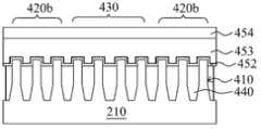
在另一个实施例中,提供了用于制造FinFET器件400的方法。参照图7和图8至图11,下文共同描述了方法300和FinFET器件400。图7为根据本发明的各方面用于制造FinFET器件400的方法300的流程图。In another embodiment, a method for fabricating
参照图7和图8与至图9,方法300开始于框302,其中,接收FinFET前体405。FinFET前体405包括半导体衬底210以及含有伪鳍420和有源鳍430的鳍结构410。形成基本上类似于结合图2和图3所述的鳍结构235的鳍结构410,使得有源鳍430在鳍形成期间经历稳定的形成环境并且在所有相关的位置中获得一致鳍的CD、轮廓和高度。Referring to FIGS. 7 and 8 through 9 ,
还参照图8,FinFET前体405还包括位于半导体衬底210中的隔离区440。隔离区440使用隔离技术(例如,STI)以限定并且电隔离FinFET器件400的各种区域。隔离区440包括二氧化硅、氮化硅、氮氧化硅、其他合适的材料或者它们的组合。通过任何合适的工艺形成隔离区440。在本实施例中,位于半导体衬底210上的鳍之间的多个沟槽用二氧化硅填充以形成隔离区440。可以在隔离区440形成之后实施退火工艺。退火工艺包括快速热退火(RTA)、激光退火工艺或者其他合适的退火工艺。随后可以实施化学机械抛光(CMP)工艺来去除多余的二氧化硅以提供基本平坦的表面。另外,如图8所示,可以通过本领域已知的合适的图案化和蚀刻工艺进一步将伪鳍420和有源鳍430中的部分鳍凹陷。Referring also to FIG. 8 , the
还参照图8,FinFET前体405还包括形成在伪鳍420和有源鳍430的一部分上的凸起的源极和漏极(S/D)结构470(称为S/D区)。可以通过一种或者多种外延或者外延(epi)工艺形成凸起的S/D结构470,使得在S/D区域中的伪鳍420和有源鳍430的凹陷表面上以晶体状态形成Si部件、SiGe部件或者其他合适的部件。外延工艺包括CVD沉积技术(例如,汽相外延(VPE)和/或超高真空CVD(UHV-CVD))、分子束外延和/或其他合适的工艺。因为伪鳍420和有源鳍430紧接,所以可以合并凸起的S/D结构470。Referring also to FIG. 8 ,
参照图9,FinFET前体405还包括:栅叠层450和栅极间隔件460,形成在半导体衬底210上方,包括位于(覆盖)鳍结构410(称为沟道区域)的部分鳍上方。栅叠层450可以包括界面层(未示出)、栅极介电层452、栅电极层453以及硬掩模层454。应该理解,栅叠层450可以包括附加层,例如,界面层、覆盖层、扩散层/势垒层、介电层、导电层、其他合适的层或者它们的组合。Referring to FIG. 9 , the
在半导体衬底210以及鳍420和430上方形成界面层。界面层包括:二氧化硅、氮氧化硅或者任何合适的材料。在界面层上方形成栅极介电层452。栅极介电层452包括介电材料,例如,二氧化硅、氮化硅、氮氧化硅、高k介电材料、其他合适的介电材料和/或它们的组合。高k介电材料的实例包括HfO2、HfSiO、HfSiON、HfTaO、HfTiO、HfZrO、氧化锆、氧化铝、氧化铪-氧化铝(HfO2-Al2O3)合金、其他合适的高k介电材料或者它们的组合。An interfacial layer is formed over the
在栅极电介质层452上方形成栅电极层453。栅电极层453包括任何合适的材料,例如,多晶硅、铝、铜、钛、钽、钨、钼、氮化钽、镍硅化物、钴硅化物、TiN、WN、TiAl、TiAlN、TaCN、TaC、TaSiN、金属合金、其他合适的材料或者它们的组合。在栅电极层453上方形成硬掩模层454。硬掩模层454可以包括任何合适的材料,例如,氮化硅、SiON、SiC、SiOC或者其他合适的材料。A
通过任何合适的工艺或者多个工艺来形成栅叠层450。例如,可以通过包括光刻图案化和蚀刻工艺的步骤形成栅叠层450。栅极间隔件460形成在栅叠层450的侧壁上并且可以包括介电材料,例如,氮化硅、碳化硅、氮氧化硅、其他合适的材料或者它们的组合。在一些实施例中,栅极间隔件用于偏移(offset)后续形成的掺杂区,例如,源极/漏极区。栅极间隔件可进一步用于设计或者修改源极/漏极区(结)轮廓。可以通过合适的沉积和蚀刻技术形成栅极间隔件。
参照图7和图10,方法300进行到步骤304,其中,形成图案化光刻胶层490以限定伪鳍组420。如图10所示,通过图案化工艺,伪鳍420被分成第一组伪鳍420a和第二组伪鳍420b。伪鳍组420a和420b可以包括一个伪鳍或者多个伪鳍。第一组伪鳍420a暴露在图案化光刻胶层490的开口内并且暴露后续的蚀刻工艺中。第二组伪鳍420b被图案化光刻胶层490(也称为覆盖有源鳍430)覆盖,使得第二组伪鳍420b(以及有源鳍430)在后续蚀刻工艺期间保持完好。另外,在所述实施例中,在形成图案化光刻胶层490之前,在半导体衬底210上形成层480。层480包括任何合适的材料并且通过任何合适的工艺形成。例如,层480可以包括各种有机材料或者无机材料。光刻胶层490涂覆在层480上并且由合适的图案化工艺进行图案化。Referring to FIGS. 7 and 10 , the
参照图7和图11a,方法300进行到步骤306,其中,通过图案化光刻胶层490的开口蚀刻第一组伪鳍420a。通过蚀刻技术(例如,在具有含氟气体的化学物质中的干蚀刻)去除第一组伪鳍420a。在本实施例中,蚀刻工艺包括两个蚀刻阶段。蚀刻工艺的第一阶段选择性去除第一组伪鳍420a的凸起的S/D结构470。蚀刻工艺的第二阶段通过由去除S/D结构470制成的开口将第一组伪鳍420a的鳍高度凹陷。在一个实施例中,部分去除第一组伪鳍420a。在另一个实施例中,完全去除第一组伪鳍420a。蚀刻工艺的第二阶段在将第一组伪鳍420a凹陷之后在半导体衬底上留下空隙495。在蚀刻第一组伪鳍420a之后,通过另一种蚀刻工艺(包括湿蚀刻、干蚀刻或者它们的组合)去除图案化光刻胶层490和层480。Referring to FIGS. 7 and 11 a , the
图11b为FinFET器件400的俯视图。参照图11b,在蚀刻第一组伪鳍420a之后,沿三条线11a-11a、11c-11c和11d-11d截取的FinFET器件400的截面图。图11a为沿图11b的线11a-11a(沿S/D区)截取的截面图。图11c为沿图11b的线11c-11c(沿沟道区域)并且平行于线11a-11a的方向截取的截面图。图11d为沿图11b的线11d-11d(沿第一组伪鳍的一个)并且垂直于线11a-11a的方向截取的截面图。如图11c和11d所示,在蚀刻工艺期间,因为通过硬掩模层454进行保护,所以具有设置在其上的栅叠层450的第一组伪鳍420a的部分保持完好。FIG. 11 b is a top view of the
参照图7和图12,方法300进行到步骤308,其中,在半导体衬底210上沉积和平坦化层间介电(ILD)层500。通过诸如CVD的合适的技术沉积ILD层500。ILD层500包括介电材料,诸如二氧化硅、氮化硅、低k介电材料或者组合。ILD层500填充通过在蚀刻工艺中去除源极和漏极结构所形成的半导体衬底上的空隙495。随后可以实施CMP工艺以提供ILD层500的基本平坦的表面。Referring to FIGS. 7 and 12 , the
FinFET器件400可以包括可以通过后续工艺形成的附加部件。例如,后续工艺可以进一步在衬底上形成被配置成连接FinFET器件400的各种部件或者结构的各种接触件/通孔/线以及多层互连部件(例如,金属层和层间介电层)。附加部件可以提供与器件的电互连。例如,多层互连件包括垂直互连件(例如,传统通孔或者接触件)以及水平互连件(例如,金属线)。可以通过包括铜、钨和/或硅化物的各种导电材料实施各种互连部件。在一个实例中,镶嵌和/或双镶嵌工艺用于形成铜相关的多层互连结构。在另一个实施例中,钨用于在接触孔中形成钨塞。
本发明提供了制造FinFET器件的许多不同的实施例,所述FinFET器件提供了优于现有技术的一种或者多种改进。在一个实施例中,用于制造FinFET器件的方法包括:提供半导体衬底,蚀刻半导体衬底以形成包括伪鳍和有源鳍的鳍结构。形成图案化光刻胶层以限定第一组伪鳍和第二组伪鳍。通过图案化光刻胶层蚀刻第一组伪鳍。在蚀刻第一组伪鳍之后在半导体衬底上形成浅沟槽隔离件(STI)。The present invention provides many different embodiments for fabricating FinFET devices that provide one or more improvements over the prior art. In one embodiment, a method for fabricating a FinFET device includes providing a semiconductor substrate, etching the semiconductor substrate to form a fin structure including a dummy fin and an active fin. A patterned photoresist layer is formed to define a first set of dummy fins and a second set of dummy fins. A first set of dummy fins is etched through the patterned photoresist layer. Shallow trench isolations (STIs) are formed on the semiconductor substrate after etching the first set of dummy fins.
在另一个实施例中,用于制造FinFET器件的方法包括接收FinFET前体。前体包括:半导体衬底,形成在半导体衬底上的伪鳍和有源鳍,形成在半导体衬底上的浅沟槽隔离(STI)区,形成在半导体衬底(包括有源鳍和伪鳍的部分)上的栅叠层以及形成在半导体衬底(包括有源鳍和伪鳍的另一部分)上的源极和漏极结构。形成图案化光刻胶层以限定第一组伪鳍和第二组鳍。实施蚀刻工艺以通过图案化光刻胶层去除第一组伪鳍(具有源极和漏极结构)的部分,In another embodiment, a method for fabricating a FinFET device includes receiving a FinFET precursor. The precursor includes: a semiconductor substrate, dummy fins and active fins formed on the semiconductor substrate, shallow trench isolation (STI) regions formed on the semiconductor substrate, formed on the semiconductor substrate (including active fins and dummy fin) and source and drain structures formed on the semiconductor substrate (including the active fin and another portion of the dummy fin). A patterned photoresist layer is formed to define a first set of dummy fins and a second set of fins. performing an etching process to remove portions of the first set of dummy fins (with source and drain structures) through the patterned photoresist layer,
在又一个实施例中,用于制造FinFET器件的方法包括提供半导体衬底,在所述半导体衬底上形成伪鳍和有源鳍,其中,有源鳍设置在伪鳍之间。在伪鳍和有源鳍上形成图案化光刻胶层。实施蚀刻工艺以去除伪鳍的暴露部分,从而在有源鳍和伪鳍的剩余部分之间形成开放空间。在形成所述开放空间之后在半导体衬底上形成浅沟槽隔离(STI)。In yet another embodiment, a method for fabricating a FinFET device includes providing a semiconductor substrate on which dummy fins and active fins are formed, wherein the active fins are disposed between the dummy fins. A patterned photoresist layer is formed on the dummy fins and the active fins. An etching process is performed to remove exposed portions of the dummy fins, thereby forming open spaces between the active fins and remaining portions of the dummy fins. Shallow trench isolation (STI) is formed on the semiconductor substrate after forming the open space.
基于上文,可以看出本发明提供了用于制造FinFET器件的方法。方法采用了新型的伪鳍方法。伪鳍方法被配置成在STI区形成之前去除一组伪鳍而保留另一组伪鳍。可选地,伪鳍方法被配置成去除S/D区中的S/D结构并且同时保留相同组伪鳍的沟道区域中的栅叠层。伪鳍方法可以在不同的工艺阶段中灵活制造以获得工艺控制的各种优势。方法表明在所有相关的位置中实现鳍的CD、轮廓和高度的一致性。Based on the above, it can be seen that the present invention provides methods for fabricating FinFET devices. The method uses a novel pseudo-fin method. The dummy fin method is configured to remove one set of dummy fins while leaving another set of dummy fins prior to STI region formation. Optionally, the dummy fin approach is configured to remove the S/D structure in the S/D region while retaining the gate stack in the channel region of the same set of dummy fins. The pseudo-fin approach can be flexibly fabricated in different process stages for various advantages of process control. The method demonstrates that uniformity in CD, profile and height of the fins is achieved in all relevant positions.
上面论述了若干实施例的部件,使得本领域普通技术人员可以更好地理解本发明的各个方面。本领域普通技术人员应该理解,可以很容易地使用本发明作为基础来设计或更改其他用于达到与这里所介绍实施例相同的目的和/或实现相同优点的工艺和结构。本领域普通技术人员也应该意识到,这种等效构造并不背离本发明的精神和范围,并且在不背离本发明的精神和范围的情况下,可以进行多种变化、替换以及改变。The components of several embodiments are discussed above so that those of ordinary skill in the art may better understand the various aspects of the invention. Those skilled in the art should understand that the present invention can be easily used as a basis to design or modify other processes and structures for achieving the same purpose and/or realizing the same advantages as the embodiments presented here. Those skilled in the art should also realize that such equivalent constructions do not depart from the spirit and scope of the invention, and that they could make various changes, substitutions and alterations herein without departing from the spirit and scope of the invention.
Claims (10)
Applications Claiming Priority (2)
| Application Number | Priority Date | Filing Date | Title |
|---|---|---|---|
| US13/490,108US8697515B2 (en) | 2012-06-06 | 2012-06-06 | Method of making a FinFET device |
| US13/490,108 | 2012-06-06 |
Publications (2)
| Publication Number | Publication Date |
|---|---|
| CN103474397Atrue CN103474397A (en) | 2013-12-25 |
| CN103474397B CN103474397B (en) | 2016-04-06 |
Family
ID=49625856
Family Applications (1)
| Application Number | Title | Priority Date | Filing Date |
|---|---|---|---|
| CN201310035323.XAActiveCN103474397B (en) | 2012-06-06 | 2013-01-29 | Manufacture the method for FINFET device |
Country Status (4)
| Country | Link |
|---|---|
| US (8) | US8697515B2 (en) |
| KR (1) | KR101388329B1 (en) |
| CN (1) | CN103474397B (en) |
| DE (2) | DE102012025824B4 (en) |
Cited By (21)
| Publication number | Priority date | Publication date | Assignee | Title |
|---|---|---|---|---|
| CN104810389A (en)* | 2014-01-23 | 2015-07-29 | 联华电子股份有限公司 | Semiconductor structure and manufacturing method thereof |
| CN105097526A (en)* | 2014-05-04 | 2015-11-25 | 中芯国际集成电路制造(上海)有限公司 | FinFET device making method |
| CN105374871A (en)* | 2014-08-22 | 2016-03-02 | 联华电子股份有限公司 | Fin structure and forming method thereof |
| CN105470286A (en)* | 2014-09-12 | 2016-04-06 | 中国科学院微电子研究所 | Semiconductor device and method for manufacturing the same |
| CN105826193A (en)* | 2015-01-07 | 2016-08-03 | 中芯国际集成电路制造(上海)有限公司 | Formation method of semiconductor device |
| CN106158648A (en)* | 2015-04-13 | 2016-11-23 | 中芯国际集成电路制造(上海)有限公司 | The method preparing Fin FET device |
| CN106505097A (en)* | 2015-09-04 | 2017-03-15 | 台湾积体电路制造股份有限公司 | Semiconductor device and manufacturing method thereof |
| CN106711220A (en)* | 2015-11-16 | 2017-05-24 | 台湾积体电路制造股份有限公司 | Fin field effect transistor and method for fabricating the same |
| US9673056B2 (en) | 2015-03-16 | 2017-06-06 | International Business Machines Corporation | Method to improve finFET cut overlay |
| CN106876336A (en)* | 2015-12-14 | 2017-06-20 | 台湾积体电路制造股份有限公司 | Semiconductor structure and its manufacture method |
| CN106952910A (en)* | 2015-12-30 | 2017-07-14 | 台湾积体电路制造股份有限公司 | Semiconductor structure and manufacturing method thereof |
| CN106952819A (en)* | 2016-01-06 | 2017-07-14 | 中芯国际集成电路制造(上海)有限公司 | Method for forming fin field effect transistor |
| CN107123649A (en)* | 2016-02-24 | 2017-09-01 | 瑞萨电子株式会社 | The method being used for producing the semiconductor devices |
| CN107680939A (en)* | 2016-08-02 | 2018-02-09 | 台湾积体电路制造股份有限公司 | Finfet and forming method thereof |
| CN107785429A (en)* | 2016-08-30 | 2018-03-09 | 台湾积体电路制造股份有限公司 | Method for forming fin on substrate |
| CN107887439A (en)* | 2016-09-29 | 2018-04-06 | 台湾积体电路制造股份有限公司 | Method for forming fin field effect transistor structure |
| CN109148451A (en)* | 2017-06-27 | 2019-01-04 | 联华电子股份有限公司 | Static random access memory unit array and forming method thereof |
| CN109585290A (en)* | 2017-09-28 | 2019-04-05 | 中芯国际集成电路制造(上海)有限公司 | Semiconductor devices and forming method thereof |
| CN110491836A (en)* | 2018-05-15 | 2019-11-22 | 中芯国际集成电路制造(上海)有限公司 | A kind of semiconductor devices and its manufacturing method, electronic device |
| CN111725137A (en)* | 2019-03-20 | 2020-09-29 | 中芯国际集成电路制造(天津)有限公司 | A method of forming a semiconductor device |
| CN114068709A (en)* | 2020-08-03 | 2022-02-18 | 中芯国际集成电路制造(上海)有限公司 | Semiconductor device and method of forming the same |
Families Citing this family (82)
| Publication number | Priority date | Publication date | Assignee | Title |
|---|---|---|---|---|
| JP2013058688A (en)* | 2011-09-09 | 2013-03-28 | Toshiba Corp | Semiconductor device manufacturing method |
| KR101908980B1 (en) | 2012-04-23 | 2018-10-17 | 삼성전자주식회사 | Field effect transistor |
| US8697515B2 (en) | 2012-06-06 | 2014-04-15 | Taiwan Semiconductor Manufacturing Company, Ltd. | Method of making a FinFET device |
| US9054212B2 (en)* | 2012-10-30 | 2015-06-09 | Globalfoundries Inc. | Fin etch and Fin replacement for FinFET integration |
| US8889561B2 (en)* | 2012-12-10 | 2014-11-18 | Globalfoundries Inc. | Double sidewall image transfer process |
| US9159576B2 (en)* | 2013-03-05 | 2015-10-13 | Qualcomm Incorporated | Method of forming finFET having fins of different height |
| US8846490B1 (en)* | 2013-03-12 | 2014-09-30 | Taiwan Semiconductor Manufacturing Company, Ltd. | Method of fabricating a FinFET device |
| US20150187701A1 (en) | 2013-03-12 | 2015-07-02 | Taiwan Semiconductor Manufacturing Company, Ltd. | Semiconductor Devices and Methods of Manufacture Thereof |
| US9263287B2 (en)* | 2013-05-27 | 2016-02-16 | United Microelectronics Corp. | Method of forming fin-shaped structure |
| US8802521B1 (en)* | 2013-06-04 | 2014-08-12 | United Microelectronics Corp. | Semiconductor fin-shaped structure and manufacturing process thereof |
| US9093496B2 (en) | 2013-07-18 | 2015-07-28 | Globalfoundries Inc. | Process for faciltiating fin isolation schemes |
| US9716174B2 (en) | 2013-07-18 | 2017-07-25 | Globalfoundries Inc. | Electrical isolation of FinFET active region by selective oxidation of sacrificial layer |
| US9224865B2 (en) | 2013-07-18 | 2015-12-29 | Globalfoundries Inc. | FinFET with insulator under channel |
| US9349730B2 (en)* | 2013-07-18 | 2016-05-24 | Globalfoundries Inc. | Fin transformation process and isolation structures facilitating different Fin isolation schemes |
| US9515184B2 (en) | 2013-09-12 | 2016-12-06 | Taiwan Semiconductor Manufacturing Company Limited | Semiconductor arrangement with multiple-height fins and substrate trenches |
| US9209178B2 (en)* | 2013-11-25 | 2015-12-08 | International Business Machines Corporation | finFET isolation by selective cyclic etch |
| US9147612B2 (en)* | 2013-11-25 | 2015-09-29 | United Microelectronics Corp. | Method for forming a semiconductor structure |
| US10056353B2 (en) | 2013-12-19 | 2018-08-21 | Taiwan Semiconductor Manufacturing Company, Ltd. | 3DIC interconnect apparatus and method |
| US9412719B2 (en) | 2013-12-19 | 2016-08-09 | Taiwan Semiconductor Manufacturing Company, Ltd. | 3DIC interconnect apparatus and method |
| KR20220025939A (en)* | 2013-12-23 | 2022-03-03 | 인텔 코포레이션 | Advanced etching techniques for straight, tall and uniform fins across multiple fin pitch structures |
| US9368408B2 (en)* | 2013-12-27 | 2016-06-14 | Infineon Technologies Dresden Gmbh | Method of manufacturing a semiconductor device with buried channel/body zone and semiconductor device |
| US9318488B2 (en)* | 2014-01-06 | 2016-04-19 | Taiwan Semiconductor Manufacturing Company Limited | Semiconductor device and formation thereof |
| US20150206759A1 (en) | 2014-01-21 | 2015-07-23 | United Microelectronics Corp. | Semiconductor structure and manufacturing method thereof |
| US9391077B2 (en)* | 2014-02-10 | 2016-07-12 | International Business Machines Corporation | SiGe and Si FinFET structures and methods for making the same |
| US9647113B2 (en) | 2014-03-05 | 2017-05-09 | International Business Machines Corporation | Strained FinFET by epitaxial stressor independent of gate pitch |
| US9196499B2 (en)* | 2014-03-26 | 2015-11-24 | Globalfoundries Inc. | Method of forming semiconductor fins |
| US9385123B2 (en)* | 2014-05-20 | 2016-07-05 | International Business Machines Corporation | STI region for small fin pitch in FinFET devices |
| US9449914B2 (en) | 2014-07-17 | 2016-09-20 | Taiwan Semiconductor Manufacturing Company, Ltd. | Stacked integrated circuits with redistribution lines |
| US10559690B2 (en) | 2014-09-18 | 2020-02-11 | International Business Machines Corporation | Embedded source/drain structure for tall FinFET and method of formation |
| US9379027B2 (en)* | 2014-10-15 | 2016-06-28 | Globalfoundries Inc. | Method of utilizing trench silicide in a gate cross-couple construct |
| US9252022B1 (en)* | 2014-11-05 | 2016-02-02 | Globalfoundries Inc. | Patterning assist feature to mitigate reactive ion etch microloading effect |
| US9287264B1 (en)* | 2014-12-05 | 2016-03-15 | Globalfoundries Inc. | Epitaxially grown silicon germanium channel FinFET with silicon underlayer |
| US10475886B2 (en)* | 2014-12-16 | 2019-11-12 | International Business Machines Corporation | Modified fin cut after epitaxial growth |
| KR102287398B1 (en) | 2015-01-14 | 2021-08-06 | 삼성전자주식회사 | Semiconductor device |
| US9397099B1 (en) | 2015-01-29 | 2016-07-19 | Taiwan Semiconductor Manufacturing Co., Ltd. | Semiconductor device having a plurality of fins and method for fabricating the same |
| KR102307467B1 (en) | 2015-03-20 | 2021-09-29 | 삼성전자주식회사 | Semiconductor device comprising active fin |
| US9601345B2 (en)* | 2015-03-27 | 2017-03-21 | International Business Machines Corporation | Fin trimming in a double sit process |
| KR102316119B1 (en) | 2015-04-02 | 2021-10-21 | 삼성전자주식회사 | Semiconductor device |
| US9704974B2 (en)* | 2015-04-16 | 2017-07-11 | Taiwan Semiconductor Manufacturing Co., Ltd. | Process of manufacturing Fin-FET device |
| US9799771B2 (en)* | 2015-04-20 | 2017-10-24 | Taiwan Semiconductor Manufacturing Co., Ltd. | FinFET and method for manufacturing the same |
| US9449881B1 (en)* | 2015-05-12 | 2016-09-20 | Globalfoundries Inc. | Methods of forming fins for FinFET semiconductor devices and the resulting devices |
| US10833175B2 (en)* | 2015-06-04 | 2020-11-10 | International Business Machines Corporation | Formation of dislocation-free SiGe finFET using porous silicon |
| US9653466B2 (en) | 2015-08-04 | 2017-05-16 | Qualcomm Incorporated | FinFET device and method of making the same |
| US9905467B2 (en) | 2015-09-04 | 2018-02-27 | Taiwan Semiconductor Manufacturing Company, Ltd. | Semiconductor device and manufacturing method thereof |
| DE102016101851B4 (en) | 2015-09-04 | 2022-09-29 | Taiwan Semiconductor Manufacturing Company, Ltd. | Semiconductor device and method of manufacturing the same |
| KR102476356B1 (en)* | 2015-10-07 | 2022-12-09 | 삼성전자주식회사 | Integrated circuit device and method of manufacturing the same |
| KR102323943B1 (en) | 2015-10-21 | 2021-11-08 | 삼성전자주식회사 | Method of manufacturing semiconductor device |
| TWI677923B (en)* | 2015-11-10 | 2019-11-21 | 聯華電子股份有限公司 | Semiconductor device and method for fabricating the same |
| US20170140992A1 (en)* | 2015-11-16 | 2017-05-18 | Taiwan Semiconductor Manufacturing Co., Ltd. | Fin field effect transistor and method for fabricating the same |
| EP3182461B1 (en)* | 2015-12-16 | 2022-08-03 | IMEC vzw | Method for fabricating finfet technology with locally higher fin-to-fin pitch |
| CN106910708B (en)* | 2015-12-22 | 2020-06-19 | 中芯国际集成电路制造(上海)有限公司 | Device with local interconnection structure and manufacturing method thereof |
| CN107026126B (en) | 2016-02-02 | 2021-01-26 | 联华电子股份有限公司 | Semiconductor element and manufacturing method thereof |
| US9704752B1 (en)* | 2016-02-26 | 2017-07-11 | Taiwan Semiconductor Manufacturing Co., Ltd. | Fin field effect transistor and method for fabricating the same |
| US9704751B1 (en)* | 2016-02-26 | 2017-07-11 | Taiwan Semiconductor Manufacturing Co., Ltd. | Semiconductor device and method for fabricating the same |
| TWI687980B (en)* | 2016-03-22 | 2020-03-11 | 聯華電子股份有限公司 | Semiconductor device and method for fabricating the same |
| KR102421730B1 (en) | 2016-04-05 | 2022-07-18 | 삼성전자주식회사 | Layout method and semiconductor device |
| US10074657B2 (en)* | 2016-04-28 | 2018-09-11 | Taiwan Semiconductor Manufacturing Company, Ltd. | Method of manufacturing fins and semiconductor device which includes fins |
| US9768072B1 (en)* | 2016-06-30 | 2017-09-19 | International Business Machines Corporation | Fabrication of a vertical fin field effect transistor with reduced dimensional variations |
| US9853131B1 (en) | 2016-07-12 | 2017-12-26 | International Business Machines Corporation | Fabrication of an isolated dummy fin between active vertical fins with tight fin pitch |
| US10032869B2 (en)* | 2016-08-17 | 2018-07-24 | Taiwan Semiconductor Manufacturing Company, Ltd. | Fin field effect transistor (FinFET) device having position-dependent heat generation and method of making the same |
| CN107887272B (en)* | 2016-09-30 | 2021-05-04 | 中芯国际集成电路制造(上海)有限公司 | Semiconductor structure and method of forming the same |
| TWI704622B (en) | 2016-11-15 | 2020-09-11 | 聯華電子股份有限公司 | Semiconductor device and method for fabricating the same |
| KR102631912B1 (en)* | 2016-12-15 | 2024-01-31 | 삼성전자주식회사 | Methods of designing a layout of a semiconductor device, and semiconductor devices |
| US9799570B1 (en) | 2017-02-13 | 2017-10-24 | International Business Machines Corporation | Fabrication of vertical field effect transistors with uniform structural profiles |
| KR102367493B1 (en)* | 2017-03-06 | 2022-02-24 | 삼성전자주식회사 | Semiconductor devices and methods of manufacturing the same |
| US10083873B1 (en)* | 2017-06-05 | 2018-09-25 | Globalfoundries Inc. | Semiconductor structure with uniform gate heights |
| US10374066B2 (en)* | 2017-07-11 | 2019-08-06 | International Business Machines Corporation | Fin and shallow trench isolation replacement to prevent gate collapse |
| DE102017124223B4 (en)* | 2017-08-30 | 2022-02-24 | Taiwan Semiconductor Manufacturing Co. Ltd. | Semiconductor structure with fins and isolation fins and method for their manufacture |
| US10276445B2 (en)* | 2017-08-31 | 2019-04-30 | Taiwan Semiconductor Manfacturing Co., Ltd. | Leakage reduction methods and structures thereof |
| CN109599336B (en)* | 2017-09-30 | 2021-05-04 | 中芯国际集成电路制造(上海)有限公司 | Semiconductor structure and method of forming the same |
| US9984933B1 (en)* | 2017-10-03 | 2018-05-29 | Globalfoundries Inc. | Silicon liner for STI CMP stop in FinFET |
| US11114549B2 (en) | 2017-11-29 | 2021-09-07 | Taiwan Semiconductor Manufacturing Co., Ltd. | Semiconductor structure cutting process and structures formed thereby |
| KR102419894B1 (en) | 2018-03-14 | 2022-07-12 | 삼성전자주식회사 | Semiconductor device including non-active fin |
| KR102593758B1 (en)* | 2018-10-10 | 2023-10-25 | 삼성전자주식회사 | Semiconductor devices |
| US11080453B2 (en)* | 2018-10-31 | 2021-08-03 | Taiwan Semiconductor Manufacturing Company Ltd. | Integrated circuit fin layout method, system, and structure |
| CN111211088B (en)* | 2018-11-21 | 2023-04-25 | 台湾积体电路制造股份有限公司 | Semiconductor device and method of forming the same |
| US11211243B2 (en) | 2018-11-21 | 2021-12-28 | Taiwan Semiconductor Manufacturing Company, Ltd. | Method of filling gaps with carbon and nitrogen doped film |
| US10818556B2 (en)* | 2018-12-17 | 2020-10-27 | United Microelectronics Corp. | Method for forming a semiconductor structure |
| CN111370488B (en)* | 2018-12-26 | 2024-04-16 | 中芯国际集成电路制造(北京)有限公司 | Semiconductor structure and method for forming the same |
| CN111785772B (en)* | 2019-04-04 | 2024-08-30 | 中芯国际集成电路制造(上海)有限公司 | Semiconductor structure and forming method thereof |
| US11264504B2 (en)* | 2020-01-24 | 2022-03-01 | Globalfoundries U.S. Inc. | Active and dummy fin structures |
| CN114695117A (en)* | 2020-12-29 | 2022-07-01 | 广州集成电路技术研究院有限公司 | A FinFET device and its formation method and electronic device |
Citations (3)
| Publication number | Priority date | Publication date | Assignee | Title |
|---|---|---|---|---|
| US6987289B2 (en)* | 2003-06-25 | 2006-01-17 | International Business Machines Corporation | High-density FinFET integration scheme |
| CN102034866A (en)* | 2009-09-24 | 2011-04-27 | 台湾积体电路制造股份有限公司 | Integrated circuit structure |
| CN102082175A (en)* | 2009-10-27 | 2011-06-01 | 台湾积体电路制造股份有限公司 | Integrated circuit structure |
Family Cites Families (31)
| Publication number | Priority date | Publication date | Assignee | Title |
|---|---|---|---|---|
| US6849549B1 (en)* | 2003-12-04 | 2005-02-01 | Taiwan Semiconductor Manufacturing Co., Ltd | Method for forming dummy structures for improved CMP and reduced capacitance |
| US7564105B2 (en)* | 2004-04-24 | 2009-07-21 | Taiwan Semiconductor Manufacturing Co., Ltd. | Quasi-plannar and FinFET-like transistors on bulk silicon |
| CN1906755A (en)* | 2004-04-30 | 2007-01-31 | 松下电器产业株式会社 | Semiconductor manufacturing method and semiconductor device |
| JP4675585B2 (en)* | 2004-06-22 | 2011-04-27 | シャープ株式会社 | Field effect transistor |
| JPWO2006006438A1 (en)* | 2004-07-12 | 2008-04-24 | 日本電気株式会社 | Semiconductor device and manufacturing method thereof |
| JP4648096B2 (en)* | 2005-06-03 | 2011-03-09 | 株式会社東芝 | Manufacturing method of semiconductor device |
| US7247887B2 (en) | 2005-07-01 | 2007-07-24 | Synopsys, Inc. | Segmented channel MOS transistor |
| CN101490822B (en)* | 2006-07-11 | 2011-03-16 | Nxp股份有限公司 | Semiconductor device and manufacturing method thereof |
| US7453125B1 (en)* | 2007-04-24 | 2008-11-18 | Infineon Technologies Ag | Double mesh finfet |
| US7888736B2 (en)* | 2007-08-29 | 2011-02-15 | International Business Machines Corporation | MUGFET with optimized fill structures |
| KR101286644B1 (en)* | 2007-11-08 | 2013-07-22 | 삼성전자주식회사 | Semiconductor device including dummy gate part and method of fabricating thereof |
| US8003466B2 (en)* | 2008-04-08 | 2011-08-23 | Advanced Micro Devices, Inc. | Method of forming multiple fins for a semiconductor device |
| US7829951B2 (en)* | 2008-11-06 | 2010-11-09 | Qualcomm Incorporated | Method of fabricating a fin field effect transistor (FinFET) device |
| US7989355B2 (en)* | 2009-02-12 | 2011-08-02 | Taiwan Semiconductor Manufacturing Company, Ltd. | Method of pitch halving |
| US8334184B2 (en)* | 2009-12-23 | 2012-12-18 | Intel Corporation | Polish to remove topography in sacrificial gate layer prior to gate patterning |
| US8937353B2 (en)* | 2010-03-01 | 2015-01-20 | Taiwan Semiconductor Manufacturing Co., Ltd. | Dual epitaxial process for a finFET device |
| US9324866B2 (en)* | 2012-01-23 | 2016-04-26 | Taiwan Semiconductor Manufacturing Company, Ltd. | Structure and method for transistor with line end extension |
| JP5646416B2 (en)* | 2011-09-01 | 2014-12-24 | 株式会社東芝 | Manufacturing method of semiconductor device |
| US8557666B2 (en)* | 2011-09-13 | 2013-10-15 | GlobalFoundries, Inc. | Methods for fabricating integrated circuits |
| US8420459B1 (en)* | 2011-10-20 | 2013-04-16 | International Business Machines Corporation | Bulk fin-field effect transistors with well defined isolation |
| US8697515B2 (en)* | 2012-06-06 | 2014-04-15 | Taiwan Semiconductor Manufacturing Company, Ltd. | Method of making a FinFET device |
| US8941156B2 (en)* | 2013-01-07 | 2015-01-27 | International Business Machines Corporation | Self-aligned dielectric isolation for FinFET devices |
| US9064900B2 (en)* | 2013-07-08 | 2015-06-23 | Globalfoundries Inc. | FinFET method comprising high-K dielectric |
| US9349730B2 (en)* | 2013-07-18 | 2016-05-24 | Globalfoundries Inc. | Fin transformation process and isolation structures facilitating different Fin isolation schemes |
| US9385048B2 (en)* | 2013-09-05 | 2016-07-05 | United Microelectronics Corp. | Method of forming Fin-FET |
| US9640533B2 (en)* | 2015-03-12 | 2017-05-02 | Globalfoundries Inc. | Methods, apparatus and system for providing source-drain epitaxy layer with lateral over-growth suppression |
| US9324713B1 (en)* | 2015-03-16 | 2016-04-26 | Globalfoundries Inc. | Eliminating field oxide loss prior to FinFET source/drain epitaxial growth |
| US9418994B1 (en)* | 2015-03-26 | 2016-08-16 | Taiwan Semiconductor Manufacturing Co., Ltd | Fin field effect transistor (FinFET) device structure |
| US9536775B2 (en)* | 2015-05-29 | 2017-01-03 | International Business Machines Corporation | Aspect ratio for semiconductor on insulator |
| US9583572B2 (en)* | 2015-06-25 | 2017-02-28 | International Business Machines Corporation | FinFET devices having silicon germanium channel fin structures with uniform thickness |
| US10032877B2 (en)* | 2016-08-02 | 2018-07-24 | Taiwan Semiconductor Manufacturing Company, Ltd. | FinFET and method of forming same |
- 2012
- 2012-06-06USUS13/490,108patent/US8697515B2/enactiveActive
- 2012-09-20KRKR1020120104415Apatent/KR101388329B1/enactiveActive
- 2012-11-15DEDE102012025824.0Apatent/DE102012025824B4/enactiveActive
- 2012-11-15DEDE102012110995.8Apatent/DE102012110995B4/enactiveActive
- 2013
- 2013-01-29CNCN201310035323.XApatent/CN103474397B/enactiveActive
- 2014
- 2014-04-09USUS14/248,403patent/US9659810B2/enactiveActive
- 2016
- 2016-12-15USUS15/380,376patent/US9805984B2/enactiveActive
- 2017
- 2017-06-30USUS15/638,589patent/US10062614B2/enactiveActive
- 2018
- 2018-08-24USUS16/111,408patent/US10546786B2/enactiveActive
- 2019
- 2019-12-27USUS16/728,098patent/US10978352B2/enactiveActive
- 2021
- 2021-04-12USUS17/301,712patent/US12033898B2/enactiveActive
- 2024
- 2024-06-25USUS18/753,406patent/US20240347390A1/enactivePending
Patent Citations (3)
| Publication number | Priority date | Publication date | Assignee | Title |
|---|---|---|---|---|
| US6987289B2 (en)* | 2003-06-25 | 2006-01-17 | International Business Machines Corporation | High-density FinFET integration scheme |
| CN102034866A (en)* | 2009-09-24 | 2011-04-27 | 台湾积体电路制造股份有限公司 | Integrated circuit structure |
| CN102082175A (en)* | 2009-10-27 | 2011-06-01 | 台湾积体电路制造股份有限公司 | Integrated circuit structure |
Cited By (46)
| Publication number | Priority date | Publication date | Assignee | Title |
|---|---|---|---|---|
| CN104810389A (en)* | 2014-01-23 | 2015-07-29 | 联华电子股份有限公司 | Semiconductor structure and manufacturing method thereof |
| CN105097526A (en)* | 2014-05-04 | 2015-11-25 | 中芯国际集成电路制造(上海)有限公司 | FinFET device making method |
| CN105097526B (en)* | 2014-05-04 | 2018-10-23 | 中芯国际集成电路制造(上海)有限公司 | The production method of FinFET |
| CN105374871A (en)* | 2014-08-22 | 2016-03-02 | 联华电子股份有限公司 | Fin structure and forming method thereof |
| CN105374871B (en)* | 2014-08-22 | 2020-05-19 | 联华电子股份有限公司 | Fin structure and forming method thereof |
| CN105470286B (en)* | 2014-09-12 | 2018-09-18 | 中国科学院微电子研究所 | Semiconductor device and method for manufacturing the same |
| CN105470286A (en)* | 2014-09-12 | 2016-04-06 | 中国科学院微电子研究所 | Semiconductor device and method for manufacturing the same |
| CN105826193A (en)* | 2015-01-07 | 2016-08-03 | 中芯国际集成电路制造(上海)有限公司 | Formation method of semiconductor device |
| US9673056B2 (en) | 2015-03-16 | 2017-06-06 | International Business Machines Corporation | Method to improve finFET cut overlay |
| US10090165B2 (en) | 2015-03-16 | 2018-10-02 | International Business Machines Corporation | Method to improve finFET cut overlay |
| CN106158648A (en)* | 2015-04-13 | 2016-11-23 | 中芯国际集成电路制造(上海)有限公司 | The method preparing Fin FET device |
| CN106158648B (en)* | 2015-04-13 | 2019-12-27 | 中芯国际集成电路制造(上海)有限公司 | Method for preparing Fin FET device |
| CN106505097A (en)* | 2015-09-04 | 2017-03-15 | 台湾积体电路制造股份有限公司 | Semiconductor device and manufacturing method thereof |
| US11018131B2 (en) | 2015-09-04 | 2021-05-25 | Taiwan Semiconductor Manufacturing Co., Ltd. | Semiconductor device and fabricating method thereof |
| CN106505097B (en)* | 2015-09-04 | 2019-12-03 | 台湾积体电路制造股份有限公司 | Semiconductor device and manufacturing method thereof |
| CN106711220B (en)* | 2015-11-16 | 2020-07-17 | 台湾积体电路制造股份有限公司 | Fin field effect transistor and manufacturing method thereof |
| CN106711220A (en)* | 2015-11-16 | 2017-05-24 | 台湾积体电路制造股份有限公司 | Fin field effect transistor and method for fabricating the same |
| TWI625827B (en)* | 2015-12-14 | 2018-06-01 | 台灣積體電路製造股份有限公司 | Semiconductor structure and manufacturing method thereof |
| US11211380B2 (en) | 2015-12-14 | 2021-12-28 | Taiwan Semiconductor Manufacturing Co., Ltd. | Semiconductor structure and manufacturing method thereof |
| CN106876336A (en)* | 2015-12-14 | 2017-06-20 | 台湾积体电路制造股份有限公司 | Semiconductor structure and its manufacture method |
| CN106876336B (en)* | 2015-12-14 | 2019-11-15 | 台湾积体电路制造股份有限公司 | Semiconductor structure and manufacturing method thereof |
| US10636787B2 (en) | 2015-12-14 | 2020-04-28 | Taiwan Semiconductor Manufacturing Co., Ltd. | Semiconductor structure and manufacturing method thereof |
| US11145510B2 (en) | 2015-12-30 | 2021-10-12 | Taiwan Semiconductor Manufacturing Co., Ltd. | FinFET device over convex insulating structure |
| CN106952910B (en)* | 2015-12-30 | 2020-12-18 | 台湾积体电路制造股份有限公司 | Semiconductor structure and method of making the same |
| CN106952910A (en)* | 2015-12-30 | 2017-07-14 | 台湾积体电路制造股份有限公司 | Semiconductor structure and manufacturing method thereof |
| CN106952819A (en)* | 2016-01-06 | 2017-07-14 | 中芯国际集成电路制造(上海)有限公司 | Method for forming fin field effect transistor |
| US11217682B2 (en) | 2016-02-24 | 2022-01-04 | Renesas Electronics Corporation | Method for manufacturing semiconductor device having thinned fins |
| CN107123649A (en)* | 2016-02-24 | 2017-09-01 | 瑞萨电子株式会社 | The method being used for producing the semiconductor devices |
| CN107680939A (en)* | 2016-08-02 | 2018-02-09 | 台湾积体电路制造股份有限公司 | Finfet and forming method thereof |
| US12176424B2 (en) | 2016-08-02 | 2024-12-24 | Taiwan Semiconductor Manufacturing Company, Ltd. | FinFET device comprising plurality of dummy protruding features |
| US11251289B2 (en) | 2016-08-02 | 2022-02-15 | Taiwan Semiconductor Manufacturing Company, Ltd. | FinFET device comprising plurality of dummy protruding features |
| CN107785429B (en)* | 2016-08-30 | 2022-03-25 | 台湾积体电路制造股份有限公司 | Method of forming fins on a substrate |
| CN107785429A (en)* | 2016-08-30 | 2018-03-09 | 台湾积体电路制造股份有限公司 | Method for forming fin on substrate |
| US11222826B2 (en) | 2016-09-29 | 2022-01-11 | Taiwan Semiconductor Manufacturing Company, Ltd. | FinFET structure and device |
| CN107887439A (en)* | 2016-09-29 | 2018-04-06 | 台湾积体电路制造股份有限公司 | Method for forming fin field effect transistor structure |
| CN107887439B (en)* | 2016-09-29 | 2022-12-02 | 台湾积体电路制造股份有限公司 | Fin-shaped field effect transistor structure and forming method thereof |
| CN111785721A (en)* | 2017-06-27 | 2020-10-16 | 联华电子股份有限公司 | static random access memory cell array |
| CN109148451B (en)* | 2017-06-27 | 2021-09-07 | 联华电子股份有限公司 | Static random access memory cell array and method of forming the same |
| CN109148451A (en)* | 2017-06-27 | 2019-01-04 | 联华电子股份有限公司 | Static random access memory unit array and forming method thereof |
| CN109585290A (en)* | 2017-09-28 | 2019-04-05 | 中芯国际集成电路制造(上海)有限公司 | Semiconductor devices and forming method thereof |
| CN110491836B (en)* | 2018-05-15 | 2021-09-14 | 中芯国际集成电路制造(上海)有限公司 | Semiconductor device, manufacturing method thereof and electronic device |
| CN110491836A (en)* | 2018-05-15 | 2019-11-22 | 中芯国际集成电路制造(上海)有限公司 | A kind of semiconductor devices and its manufacturing method, electronic device |
| CN111725137A (en)* | 2019-03-20 | 2020-09-29 | 中芯国际集成电路制造(天津)有限公司 | A method of forming a semiconductor device |
| CN111725137B (en)* | 2019-03-20 | 2023-06-23 | 中芯国际集成电路制造(天津)有限公司 | Method for forming semiconductor device |
| CN114068709A (en)* | 2020-08-03 | 2022-02-18 | 中芯国际集成电路制造(上海)有限公司 | Semiconductor device and method of forming the same |
| CN114068709B (en)* | 2020-08-03 | 2023-08-18 | 中芯国际集成电路制造(上海)有限公司 | Semiconductor device and method of forming the same |
Also Published As
| Publication number | Publication date |
|---|---|
| US20170098582A1 (en) | 2017-04-06 |
| US20180012809A1 (en) | 2018-01-11 |
| DE102012110995A1 (en) | 2013-12-12 |
| US20240347390A1 (en) | 2024-10-17 |
| US9659810B2 (en) | 2017-05-23 |
| DE102012110995B4 (en) | 2018-04-12 |
| US10546786B2 (en) | 2020-01-28 |
| US20130330889A1 (en) | 2013-12-12 |
| US10978352B2 (en) | 2021-04-13 |
| US12033898B2 (en) | 2024-07-09 |
| US20210305102A1 (en) | 2021-09-30 |
| US9805984B2 (en) | 2017-10-31 |
| US10062614B2 (en) | 2018-08-28 |
| US20140291770A1 (en) | 2014-10-02 |
| US8697515B2 (en) | 2014-04-15 |
| DE102012025824B4 (en) | 2021-06-02 |
| CN103474397B (en) | 2016-04-06 |
| DE102012025824A1 (en) | 2018-05-30 |
| KR20130137068A (en) | 2013-12-16 |
| KR101388329B1 (en) | 2014-04-22 |
| US20200144130A1 (en) | 2020-05-07 |
| US20190057908A1 (en) | 2019-02-21 |
Similar Documents
| Publication | Publication Date | Title |
|---|---|---|
| CN103474397B (en) | Manufacture the method for FINFET device | |
| CN110556374B (en) | FinFET device structure and method with contacts over dielectric gate | |
| US10923353B2 (en) | Fin field effect transistor (FinFET) device with controlled end-to-end critical dimension and method for forming the same | |
| KR101745793B1 (en) | Semiconductor device having a plurality of fins and method for fabricating the same | |
| CN103426882B (en) | CMOS device and forming method thereof | |
| CN102214579B (en) | Manufacturing method of semiconductor element and semiconductor element | |
| CN108807380B (en) | Semiconductor structures and methods of forming integrated circuit structures | |
| CN107039526B (en) | Semiconductor device and method for manufacturing the same | |
| CN103187418B (en) | A kind of CMOS FinFET and forming method thereof | |
| CN105023944B (en) | FinFET with high-K metal gate stack | |
| CN105047711B (en) | For the structures and methods of FINFET device | |
| US9496259B2 (en) | FinFET semiconductor device having fins with stronger structural strength | |
| CN114300363A (en) | Semiconductor element and manufacturing method thereof | |
| TWI783302B (en) | Semiconductor device and formation method thereof | |
| US11521858B2 (en) | Method and device for forming metal gate electrodes for transistors | |
| CN106910686B (en) | Semiconductor device, preparation method thereof and electronic device |
Legal Events
| Date | Code | Title | Description |
|---|---|---|---|
| C06 | Publication | ||
| PB01 | Publication | ||
| C10 | Entry into substantive examination | ||
| SE01 | Entry into force of request for substantive examination | ||
| C14 | Grant of patent or utility model | ||
| GR01 | Patent grant |