CN103460391A - Semiconductor device and display device - Google Patents
Semiconductor device and display deviceDownload PDFInfo
- Publication number
- CN103460391A CN103460391ACN2012800163262ACN201280016326ACN103460391ACN 103460391 ACN103460391 ACN 103460391ACN 2012800163262 ACN2012800163262 ACN 2012800163262ACN 201280016326 ACN201280016326 ACN 201280016326ACN 103460391 ACN103460391 ACN 103460391A
- Authority
- CN
- China
- Prior art keywords
- electrode
- diode element
- electrically connected
- semiconductor device
- layer
- Prior art date
- Legal status (The legal status is an assumption and is not a legal conclusion. Google has not performed a legal analysis and makes no representation as to the accuracy of the status listed.)
- Pending
Links
Images


Classifications
- H—ELECTRICITY
- H10—SEMICONDUCTOR DEVICES; ELECTRIC SOLID-STATE DEVICES NOT OTHERWISE PROVIDED FOR
- H10D—INORGANIC ELECTRIC SEMICONDUCTOR DEVICES
- H10D30/00—Field-effect transistors [FET]
- H10D30/60—Insulated-gate field-effect transistors [IGFET]
- H10D30/67—Thin-film transistors [TFT]
- H10D30/6704—Thin-film transistors [TFT] having supplementary regions or layers in the thin films or in the insulated bulk substrates for controlling properties of the device
- H10D30/6713—Thin-film transistors [TFT] having supplementary regions or layers in the thin films or in the insulated bulk substrates for controlling properties of the device characterised by the properties of the source or drain regions, e.g. compositions or sectional shapes
- H10D30/6715—Thin-film transistors [TFT] having supplementary regions or layers in the thin films or in the insulated bulk substrates for controlling properties of the device characterised by the properties of the source or drain regions, e.g. compositions or sectional shapes characterised by the doping profiles, e.g. having lightly-doped source or drain extensions
- G—PHYSICS
- G02—OPTICS
- G02F—OPTICAL DEVICES OR ARRANGEMENTS FOR THE CONTROL OF LIGHT BY MODIFICATION OF THE OPTICAL PROPERTIES OF THE MEDIA OF THE ELEMENTS INVOLVED THEREIN; NON-LINEAR OPTICS; FREQUENCY-CHANGING OF LIGHT; OPTICAL LOGIC ELEMENTS; OPTICAL ANALOGUE/DIGITAL CONVERTERS
- G02F1/00—Devices or arrangements for the control of the intensity, colour, phase, polarisation or direction of light arriving from an independent light source, e.g. switching, gating or modulating; Non-linear optics
- G02F1/01—Devices or arrangements for the control of the intensity, colour, phase, polarisation or direction of light arriving from an independent light source, e.g. switching, gating or modulating; Non-linear optics for the control of the intensity, phase, polarisation or colour
- G02F1/13—Devices or arrangements for the control of the intensity, colour, phase, polarisation or direction of light arriving from an independent light source, e.g. switching, gating or modulating; Non-linear optics for the control of the intensity, phase, polarisation or colour based on liquid crystals, e.g. single liquid crystal display cells
- G02F1/133—Constructional arrangements; Operation of liquid crystal cells; Circuit arrangements
- G02F1/136—Liquid crystal cells structurally associated with a semi-conducting layer or substrate, e.g. cells forming part of an integrated circuit
- G02F1/1362—Active matrix addressed cells
- G02F1/136204—Arrangements to prevent high voltage or static electricity failures
- G—PHYSICS
- G02—OPTICS
- G02F—OPTICAL DEVICES OR ARRANGEMENTS FOR THE CONTROL OF LIGHT BY MODIFICATION OF THE OPTICAL PROPERTIES OF THE MEDIA OF THE ELEMENTS INVOLVED THEREIN; NON-LINEAR OPTICS; FREQUENCY-CHANGING OF LIGHT; OPTICAL LOGIC ELEMENTS; OPTICAL ANALOGUE/DIGITAL CONVERTERS
- G02F1/00—Devices or arrangements for the control of the intensity, colour, phase, polarisation or direction of light arriving from an independent light source, e.g. switching, gating or modulating; Non-linear optics
- G02F1/01—Devices or arrangements for the control of the intensity, colour, phase, polarisation or direction of light arriving from an independent light source, e.g. switching, gating or modulating; Non-linear optics for the control of the intensity, phase, polarisation or colour
- G02F1/13—Devices or arrangements for the control of the intensity, colour, phase, polarisation or direction of light arriving from an independent light source, e.g. switching, gating or modulating; Non-linear optics for the control of the intensity, phase, polarisation or colour based on liquid crystals, e.g. single liquid crystal display cells
- G02F1/133—Constructional arrangements; Operation of liquid crystal cells; Circuit arrangements
- G02F1/136—Liquid crystal cells structurally associated with a semi-conducting layer or substrate, e.g. cells forming part of an integrated circuit
- G02F1/1362—Active matrix addressed cells
- G02F1/1368—Active matrix addressed cells in which the switching element is a three-electrode device
- H—ELECTRICITY
- H10—SEMICONDUCTOR DEVICES; ELECTRIC SOLID-STATE DEVICES NOT OTHERWISE PROVIDED FOR
- H10D—INORGANIC ELECTRIC SEMICONDUCTOR DEVICES
- H10D30/00—Field-effect transistors [FET]
- H10D30/60—Insulated-gate field-effect transistors [IGFET]
- H10D30/67—Thin-film transistors [TFT]
- H10D30/674—Thin-film transistors [TFT] characterised by the active materials
- H10D30/6755—Oxide semiconductors, e.g. zinc oxide, copper aluminium oxide or cadmium stannate
- H—ELECTRICITY
- H10—SEMICONDUCTOR DEVICES; ELECTRIC SOLID-STATE DEVICES NOT OTHERWISE PROVIDED FOR
- H10D—INORGANIC ELECTRIC SEMICONDUCTOR DEVICES
- H10D86/00—Integrated devices formed in or on insulating or conducting substrates, e.g. formed in silicon-on-insulator [SOI] substrates or on stainless steel or glass substrates
- H10D86/40—Integrated devices formed in or on insulating or conducting substrates, e.g. formed in silicon-on-insulator [SOI] substrates or on stainless steel or glass substrates characterised by multiple TFTs
- H10D86/421—Integrated devices formed in or on insulating or conducting substrates, e.g. formed in silicon-on-insulator [SOI] substrates or on stainless steel or glass substrates characterised by multiple TFTs having a particular composition, shape or crystalline structure of the active layer
- H10D86/423—Integrated devices formed in or on insulating or conducting substrates, e.g. formed in silicon-on-insulator [SOI] substrates or on stainless steel or glass substrates characterised by multiple TFTs having a particular composition, shape or crystalline structure of the active layer comprising semiconductor materials not belonging to the Group IV, e.g. InGaZnO
- H—ELECTRICITY
- H10—SEMICONDUCTOR DEVICES; ELECTRIC SOLID-STATE DEVICES NOT OTHERWISE PROVIDED FOR
- H10D—INORGANIC ELECTRIC SEMICONDUCTOR DEVICES
- H10D86/00—Integrated devices formed in or on insulating or conducting substrates, e.g. formed in silicon-on-insulator [SOI] substrates or on stainless steel or glass substrates
- H10D86/40—Integrated devices formed in or on insulating or conducting substrates, e.g. formed in silicon-on-insulator [SOI] substrates or on stainless steel or glass substrates characterised by multiple TFTs
- H10D86/481—Integrated devices formed in or on insulating or conducting substrates, e.g. formed in silicon-on-insulator [SOI] substrates or on stainless steel or glass substrates characterised by multiple TFTs integrated with passive devices, e.g. auxiliary capacitors
- H—ELECTRICITY
- H10—SEMICONDUCTOR DEVICES; ELECTRIC SOLID-STATE DEVICES NOT OTHERWISE PROVIDED FOR
- H10D—INORGANIC ELECTRIC SEMICONDUCTOR DEVICES
- H10D86/00—Integrated devices formed in or on insulating or conducting substrates, e.g. formed in silicon-on-insulator [SOI] substrates or on stainless steel or glass substrates
- H10D86/40—Integrated devices formed in or on insulating or conducting substrates, e.g. formed in silicon-on-insulator [SOI] substrates or on stainless steel or glass substrates characterised by multiple TFTs
- H10D86/60—Integrated devices formed in or on insulating or conducting substrates, e.g. formed in silicon-on-insulator [SOI] substrates or on stainless steel or glass substrates characterised by multiple TFTs wherein the TFTs are in active matrices
- G—PHYSICS
- G02—OPTICS
- G02F—OPTICAL DEVICES OR ARRANGEMENTS FOR THE CONTROL OF LIGHT BY MODIFICATION OF THE OPTICAL PROPERTIES OF THE MEDIA OF THE ELEMENTS INVOLVED THEREIN; NON-LINEAR OPTICS; FREQUENCY-CHANGING OF LIGHT; OPTICAL LOGIC ELEMENTS; OPTICAL ANALOGUE/DIGITAL CONVERTERS
- G02F1/00—Devices or arrangements for the control of the intensity, colour, phase, polarisation or direction of light arriving from an independent light source, e.g. switching, gating or modulating; Non-linear optics
- G02F1/01—Devices or arrangements for the control of the intensity, colour, phase, polarisation or direction of light arriving from an independent light source, e.g. switching, gating or modulating; Non-linear optics for the control of the intensity, phase, polarisation or colour
- G02F1/13—Devices or arrangements for the control of the intensity, colour, phase, polarisation or direction of light arriving from an independent light source, e.g. switching, gating or modulating; Non-linear optics for the control of the intensity, phase, polarisation or colour based on liquid crystals, e.g. single liquid crystal display cells
- G02F1/133—Constructional arrangements; Operation of liquid crystal cells; Circuit arrangements
- G02F1/136—Liquid crystal cells structurally associated with a semi-conducting layer or substrate, e.g. cells forming part of an integrated circuit
- G02F1/1362—Active matrix addressed cells
- G02F1/1365—Active matrix addressed cells in which the switching element is a two-electrode device
- G—PHYSICS
- G02—OPTICS
- G02F—OPTICAL DEVICES OR ARRANGEMENTS FOR THE CONTROL OF LIGHT BY MODIFICATION OF THE OPTICAL PROPERTIES OF THE MEDIA OF THE ELEMENTS INVOLVED THEREIN; NON-LINEAR OPTICS; FREQUENCY-CHANGING OF LIGHT; OPTICAL LOGIC ELEMENTS; OPTICAL ANALOGUE/DIGITAL CONVERTERS
- G02F2202/00—Materials and properties
- G02F2202/22—Antistatic materials or arrangements
Landscapes
- Physics & Mathematics (AREA)
- Nonlinear Science (AREA)
- Engineering & Computer Science (AREA)
- Microelectronics & Electronic Packaging (AREA)
- Mathematical Physics (AREA)
- Chemical & Material Sciences (AREA)
- Crystallography & Structural Chemistry (AREA)
- General Physics & Mathematics (AREA)
- Optics & Photonics (AREA)
- Thin Film Transistor (AREA)
- Devices For Indicating Variable Information By Combining Individual Elements (AREA)
- Liquid Crystal (AREA)
Abstract
Translated fromChinese
Description
Translated fromChinese技术领域technical field
本发明涉及具备薄膜晶体管(TFT)的半导体装置和具有这样的半导体装置的显示装置。The present invention relates to a semiconductor device including a thin film transistor (TFT) and a display device including such a semiconductor device.
背景技术Background technique
近年来,使用具有铟(In)、锌(Zn)或镓(Ga)等的氧化物半导体层的TFT(氧化物半导体TFT)的开发积极地进行(例如专利文献1~3)。氧化物半导体TFT具有迁移率高的特性,因此,例如被期待能够使具备氧化物半导体TFT的液晶显示装置的显示品质提高。In recent years, development of a TFT (oxide semiconductor TFT) using an oxide semiconductor layer such as indium (In), zinc (Zn), or gallium (Ga) has been actively developed (for example,
另一方面,半导体装置的制造工艺包括容易产生静电的工序,由于静电,会发生特性改变、或静电击穿,因此,存在具备TFT的半导体装置的良品率下降的问题。特别是在液晶显示装置的TFT基板(半导体装置)中,存在由产生的静电引起的成品率下降的问题。On the other hand, the manufacturing process of a semiconductor device includes a process where static electricity is likely to be generated. Due to the static electricity, a characteristic change or electrostatic breakdown may occur. Therefore, there is a problem that the yield rate of a semiconductor device including a TFT is lowered. Especially in TFT substrates (semiconductor devices) of liquid crystal display devices, there is a problem of a decrease in yield due to generated static electricity.
因此,提出了具备用于防止由静电引起的损坏的各种单元的TFT基板(例如专利文献4)。专利文献4中公开了为了防止静电击穿而设置有二极管环的TFT基板。Therefore, a TFT substrate including various cells for preventing damage due to static electricity has been proposed (for example, Patent Document 4).
现有技术文献prior art literature
专利文献patent documents
专利文献1:日本特开2003-298062号公报Patent Document 1: Japanese Patent Laid-Open No. 2003-298062
专利文献2:日本特开2009-253204号公报Patent Document 2: Japanese Patent Laid-Open No. 2009-253204
专利文献3:日本特开2008-166716号公报Patent Document 3: Japanese Patent Laid-Open No. 2008-166716
专利文献4:日本特开平11-271722号公报Patent Document 4: Japanese Patent Application Laid-Open No. 11-271722
发明内容Contents of the invention
发明要解决的技术问题The technical problem to be solved by the invention
但是,本发明人发现:即使在具备氧化物半导体TFT的半导体装置中采用专利文献4中公开的静电防止用的二极管环,在进行驱动的电压附近,氧化物半导体层的电阻值小,作为静电防止用的二极管环也存在不良情况。对于在绝缘基板上具备迁移率高的氧化物半导体TFT并且具备双向的静电防止用二极管环的半导体装置的制造方法,这是共同的技术问题。However, the inventors of the present invention have found that even if the diode ring for preventing static electricity disclosed in
本发明是鉴于上述问题而做出的,其目的在于,提供在具备氧化物半导体TFT的半导体装置中,能够防止由静电引起的损坏的半导体装置和具备这样的半导体装置的显示装置。The present invention has been made in view of the above problems, and an object of the present invention is to provide a semiconductor device capable of preventing damage due to static electricity in a semiconductor device including an oxide semiconductor TFT, and a display device including such a semiconductor device.
用于解决技术问题的手段Means used to solve technical problems
本发明的实施方式的半导体装置具有:绝缘基板;在上述绝缘基板上形成的多个配线;多个薄膜晶体管;和多个二极管元件,该多个二极管元件各自将上述多个配线中的2条配线相互电连接,上述半导体装置的特征在于,上述多个二极管元件各自具有:与上述薄膜晶体管的栅极电极由相同的导电膜形成的第一电极;在上述第一电极上形成的氧化物半导体层;和与上述薄膜晶体管的源极电极由相同的导电膜形成,并且与上述氧化物半导体层接触的第二电极和第三电极,上述氧化物半导体层在上述第一电极与上述第二电极之间、以及上述第一电极与上述第三电极之间分别具有偏置区域,在从上述绝缘基板的法线方向看时,上述偏置区域与上述第一电极不重叠。A semiconductor device according to an embodiment of the present invention includes: an insulating substrate; a plurality of wirings formed on the insulating substrate; a plurality of thin film transistors; and a plurality of diode elements each connecting one of the plurality of wirings to The two wirings are electrically connected to each other, and the semiconductor device is characterized in that each of the plurality of diode elements has: a first electrode formed of the same conductive film as the gate electrode of the thin film transistor; an oxide semiconductor layer; and a second electrode and a third electrode which are formed of the same conductive film as the source electrode of the thin film transistor and are in contact with the oxide semiconductor layer, the oxide semiconductor layer being between the first electrode and the There are offset regions between the second electrodes and between the first electrode and the third electrode, and the offset regions do not overlap with the first electrodes when viewed from the normal direction of the insulating substrate.
在一个实施方式中,在从上述绝缘基板的法线方向看时,上述偏置区域与上述第一电极、第二电极和第三电极均不重叠。In one embodiment, when viewed from the normal direction of the insulating substrate, the offset region does not overlap any of the first electrode, the second electrode, and the third electrode.
在一个实施方式中,上述偏置区域的与沟道方向平行的方向的宽度为3μm以上5μm以下。In one embodiment, the width of the offset region in a direction parallel to the channel direction is not less than 3 μm and not more than 5 μm.
在一个实施方式中,上述多个二极管元件彼此方向相反地并联地电连接。In one embodiment, the plurality of diode elements described above are electrically connected in parallel in opposite directions.
在一个实施方式中,上述氧化物半导体层含有In、Ga和Zn中的至少1种。In one embodiment, the oxide semiconductor layer contains at least one of In, Ga, and Zn.
在一个实施方式中,上述多个配线包括多个源极配线和多个栅极配线,上述多个二极管元件包括将2条源极配线相互电连接的二极管元件和将2条栅极配线相互电连接的二极管元件中的至少1种。In one embodiment, the plurality of wirings include a plurality of source wirings and a plurality of gate wirings, and the plurality of diode elements include diode elements electrically connecting two source wirings to each other and two gate wirings. At least one type of diode elements electrically connected to each other by pole wiring.
在一个实施方式中,上述多个配线还包括多个辅助电容配线、共用电极配线和多个检查信号配线中的任意配线,上述多个二极管元件包括:将2条源极配线相互电连接的二极管元件、将2条栅极配线相互电连接的二极管元件、将栅极配线与辅助电容配线相互电连接的二极管元件、将源极配线与辅助电容配线相互电连接的二极管元件、将辅助电容配线与共用电极配线相互电连接的二极管元件、将栅极配线与共用电极配线相互电连接的二极管元件、将源极配线与共用电极配线相互电连接的二极管元件、或将2条检查信号配线相互电连接的二极管元件。In one embodiment, the plurality of wirings further includes any of a plurality of auxiliary capacitor wirings, a common electrode wiring, and a plurality of inspection signal wirings, and the plurality of diode elements include: A diode element that electrically connects two gate lines, a diode element that electrically connects two gate lines, a diode element that electrically connects a gate line and a storage capacitor line, and a source line that connects a storage capacitor line to each other. A diode element electrically connected, a diode element electrically connected to the auxiliary capacitor line and the common electrode line, a diode element electrically connected to the gate line and the common electrode line, a source line and the common electrode line A diode element electrically connected to each other, or a diode element electrically connected to two inspection signal lines.
本发明的实施方式的显示装置具有上述的半导体装置。A display device according to an embodiment of the present invention includes the above-mentioned semiconductor device.
发明效果Invention effect
根据本发明,能提供在具备氧化物半导体TFT的半导体装置中,能够防止由静电引起的损坏的半导体装置和具备这样的半导体装置的显示装置。According to the present invention, it is possible to provide a semiconductor device including an oxide semiconductor TFT that can prevent damage due to static electricity, and a display device including such a semiconductor device.
附图说明Description of drawings
图1(a)是本发明的实施方式的半导体装置100的等价电路图,(b)是表示二极管元件10的电压-电流特性的曲线图。FIG. 1( a ) is an equivalent circuit diagram of a
图2(a)是具备二极管元件10的半导体装置100的示意性的平面图,(b)是沿(a)的I-I’线的示意性的截面图。Fig. 2(a) is a schematic plan view of a
图3是对二极管元件10的电特性进行说明的曲线图。FIG. 3 is a graph illustrating electrical characteristics of the
图4(a)~(e)是对二极管元件10的制造工序进行说明的图。4( a ) to ( e ) are diagrams illustrating the manufacturing process of the
图5(a)~(e)是对像素用TFT的制造工序进行说明的图。5( a ) to ( e ) are diagrams illustrating the manufacturing process of the pixel TFT.
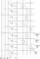
图6是对检查信号配线进行说明的等价电路图。FIG. 6 is an equivalent circuit diagram illustrating inspection signal wiring.
具体实施方式Detailed ways
以下,参照附图,对本发明的实施方式的半导体装置的制造方法和通过这样的制造方法制造的半导体装置(在此为液晶显示装置用的TFT基板)的结构进行说明。本实施方式的TFT基板包括各种显示装置(例如液晶显示装置或EL显示装置)的TFT基板。Hereinafter, a method of manufacturing a semiconductor device according to an embodiment of the present invention and a structure of a semiconductor device (here, a TFT substrate for a liquid crystal display device) manufactured by such a manufacturing method will be described with reference to the drawings. The TFT substrate of this embodiment includes TFT substrates of various display devices (for example, liquid crystal display devices or EL display devices).
以下,参照图1和图2,对本发明的实施方式的半导体装置100进行说明。图1(a)是半导体装置100的等价电路图,图1(b)是表示二极管元件10的电压(V)-电流(I)特性的曲线图。此外,图1(a)中也记载有液晶电容40。Hereinafter, a
如图1(a)所示,半导体装置100具备:相互平行地排列的多个栅极配线14;与栅极配线14正交的多个源极配线16;分别设置在由栅极配线14和源极配线16包围的矩形区域的像素电极(未图示);和配置在栅极配线14与源极配线16的交叉部附近的薄膜晶体管(有时也称为像素用TFT)50。栅极配线14和源极配线16分别与薄膜晶体管50电连接。栅极配线14与栅极端子14t电连接,源极配线16与源极端子16t电连接。栅极端子14t和源极端子16t分别与外部配线(未图示)电连接。薄膜晶体管50与像素电极电连接,作为对各像素的液晶电容(像素电容)40施加电压的开关元件发挥作用。液晶电容40由一对电极和液晶层形成,与像素用TFT的漏极电极连接的电极为像素电极,另一个电极为相对电极。相对电极形成在以隔着液晶层与TFT基板相对的方式配置的相对基板上。此外,在IPS(In-Plane Switching:面内开关)模式或FFS(Fringe Field Switching:边缘场开关)模式的液晶显示装置的情况下,不在相对基板上形成相对电极。As shown in FIG. 1( a), the
在相互相邻的2条源极配线(例如源极配线16(m)与16(m+1))之间,形成有具有与薄膜晶体管50的氧化物半导体层由相同的氧化物半导体膜形成的氧化物半导体层的短路环用的二极管元件10A和10B。在此例示的二极管元件10A和10B具有使TFT的源极电极和栅极电极短路的结构,也被称为“TFT型二极管”。Between two source wirings adjacent to each other (for example, source wirings 16(m) and 16(m+1)), an oxide semiconductor layer made of the same oxide semiconductor layer as that of the
二极管元件10A和二极管元件10B中,电流流动的方向相互相反。例如,二极管元件10A(m)从源极配线16(m)向源极配线16(m+1)流动电流,二极管元件10B(m)从源极配线16(m+1)向源极配线16(m)流动电流。如在此例示的那样,通过在所有相互相邻的2条源极配线将二极管元件10A和10B并联连接,形成由二极管元件10A构成的短路环20A和由二极管元件10B构成的短路环20B,短路环20A和短路环20B构成短路环20。短路环20能够向双方流动电流(扩散电荷)。二极管元件10A和10B也可以配置在栅极配线14(n)与栅极配线14(n+1)之间,将栅极配线14(n)与栅极配线14(n+1)电连接。In the
另外,半导体装置100还可以包括多个辅助电容配线、共用电极配线或多个检查信号配线。在该情况下,二极管元件10A和10B可以配置在栅极配线14与辅助电容配线之间、源极配线与辅助电容配线之间、辅助电容配线与共用电极配线之间、栅极配线与共用电极配线之间、源极配线与共用电极配线之间、或者2条检查信号配线之间,将各个配线电连接。在此,共用电极配线,例如,在半导体装置100用于液晶显示装置的情况下,是和在与半导体装置100相对的基板上形成的相对电极电连接的配线。另外,检查信号配线是用于检查像素用TFT的电特性的配线。此外,关于检查信号配线的详细情况,已在日本特开2005-122209号公报和美国专利第6624857号说明书中公开。为了参考,本说明书中援用日本特开2005-122209号公报和美国专利第6624857号说明书中公开的全部内容。In addition, the
图6是对检查信号配线进行说明的等价电路图。如图6所示,在半导体装置100中,例如设置有3条检查信号配线26R、26G、26B、检查用TFT27a和检查用控制信号线28。各检查信号配线26R、26G、26B各自例如与检查用TFT27a的漏极电极电连接。另外,各源极配线16(16(m)~16(m+3))例如与检查用TFT27a的源极电极电连接。检查用TFT27a的栅极电极与检查用控制信号线28电连接,对检查用TFT27a进行控制。二极管元件10例如配置在与电连接到相同的检查用信号配线26R、26G、26B的检查用TFT27a连接的源极配线16(m)与16(m+3)之间,与源极配线16(m)和源极配线16(m+3)连接。FIG. 6 is an equivalent circuit diagram illustrating inspection signal wiring. As shown in FIG. 6 , in the
图1(b)所示的曲线图是表示二极管元件10的电压(V)-电流(I)特性的曲线图。The graph shown in FIG. 1( b ) is a graph showing the voltage (V)-current (I) characteristic of the
如图1(b)所示,二极管元件10的击穿电压为20V以上400V以下。在对二极管元件10的半导体层施加击穿电压以下的电压的情况下,在二极管元件10中不会流动电流,因此,源极配线16(m)与源极配线16(m+3)之间绝缘。当对二极管元件10的半导体层施加超过击穿电压的电压时,在二极管元件10中流动电流,源极配线16(m)与源极配线16(m+3)电连接。As shown in FIG. 1( b ), the breakdown voltage of the
另外,虽然没有图示,但是也可以在相互相邻的2条栅极配线(例如栅极配线14(n)与14(n+1))之间形成短路环用的二极管元件。另外,也可以在栅极配线14与源极配线16之间形成短路环用的二极管元件,并将源极配线用的短路环与栅极配线用的短路环相互连接。In addition, although not shown, a diode element for a short-circuit ring may be formed between two mutually adjacent gate wirings (for example, gate wirings 14 ( n ) and 14 ( n+1 )). Alternatively, a diode element for a short-circuit ring may be formed between the
在半导体装置100中,当有静电从外部进入任一个源极配线16(或/和栅极配线14)时,与源极配线16(或/和栅极配线14)电连接的二极管元件10A和10B的栅极导通,电荷依次向相邻的源极配线16(或/和栅极配线14)扩散。其结果,全部源极配线16(或/和栅极配线14)成为相等电位,因此,能够抑制薄膜晶体管50由于静电而受到损坏。In the
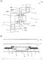
图2是对短路环用的二极管元件10(10A和10B)进行说明的图。图2(a)是二极管元件10的示意性的平面图,图2(b)是沿图2(a)的I-I’线的截面图。FIG. 2 is a diagram illustrating diode elements 10 ( 10A and 10B) for short rings. FIG. 2( a ) is a schematic plan view of the
如图2(a)和图2(b)所示,二极管元件10具有:与在绝缘基板1上形成的薄膜晶体管(例如像素用TFT)50(未图示)的栅极电极由相同的导电膜形成的第一电极3(3a和3b);在第一电极3上形成的第一绝缘层4;形成在第一绝缘层4上,并且与薄膜晶体管50的氧化物半导体层由相同的氧化物半导体膜形成的氧化物半导体层5(5a和5b);和与氧化物半导体层5接触,并且与薄膜晶体管50的源极电极由相同的导电膜形成的第二电极6和第三电极7。在氧化物半导体层5的第一电极3与第二电极6之间、以及第一电极3与第三电极7之间,分别形成有偏置区域19。在从绝缘基板1的法线方向看时,偏置区域19与第一电极3不重叠。另外,优选在从绝缘基板1的法线方向看时,偏置区域19与第一电极3、第二电极6和第三电极7均不重叠。第二电极6与源极配线16(m)电连接,第三电极7与源极配线16(m+1)电连接。另外,二极管元件10A的第一电极3a通过透明电极11与第二电极6电连接。二极管元件10B的第一电极3b通过透明电极11与第三电极7电连接。As shown in FIG. 2( a ) and FIG. 2( b ), the
另外,以覆盖氧化物半导体层5的方式形成有第二绝缘层8,在第二绝缘层8上形成有感光性的有机绝缘层9。另外,也可以在氧化物半导体层5之上形成刻蚀阻挡层。另外,也有可以不形成有机绝缘层9的情况。In addition, a second
二极管元件10的沟道长度L例如为30μm,沟道宽度W例如为5μm,偏置区域19的与沟道方向平行的方向的宽度(偏置区域宽度)W’例如为3μm。另外,沟道长度L例如优选为10μm以上50μm以下,沟道宽度W例如优选为2μm以上10μm以下,偏置区域宽度W’优选为1.5μm以上5μm以下。当采用这样的沟道长度L、沟道宽度W和偏置区域宽度W’时,二极管元件10作为具有如上所述的特性的短路环用的二极管元件发挥作用。The channel length L of the
第一电极3、第二电极6、第三电极7、栅极配线14和源极配线16具有例如下层为Ti(钛)层且上层为Cu(铜)层的叠层结构。下层的厚度例如为30nm~150nm。上层的厚度例如为200nm~500nm。另外,例如上层可以不是Cu层而是Al(铝)层,另外,第一电极3、第二电极6、第三电极7和源极配线16也可以具有例如仅具有Ti层的单层结构。The
第一绝缘层4和第二绝缘层8具有例如含有SiNx(氮化硅)的单层结构。第一绝缘层4和第二绝缘层8的厚度例如分别为100nm~500nm。The first insulating
氧化物半导体层5例如为含有In(铟)、Ga(镓)和Zn(锌)中的至少任1种元素的氧化物半导体层。在本实施方式中,氧化物半导体层5为含有In、Ga和Zn的非晶氧化物半导体层(a-IGZO层)。氧化物半导体层5的厚度例如为20nm~200nm。The
有机绝缘层9的厚度例如为3μm。The thickness of the organic insulating layer 9 is, for example, 3 μm.
透明电极11例如由ITO(Indium Tin Oxide:铟锡氧化物)形成。透明电极11的厚度例如为50nm~200nm。The
接着,参照图3,对二极管元件10的电特性进行说明。图3是表示以下说明的元件的电压(V)-电流(I)特性的曲线图。图3中的曲线C1是表示半导体装置100具有的像素用的氧化物半导体TFT的栅极电压(V)-电流(I)特性的曲线。曲线C2是表示二极管元件10的电压(V)-电流(I)特性的曲线。曲线C3是表示具有一般使用的非晶硅(a-Si)层作为半导体层的短路环用的二极管元件(a-Si二极管元件)的电压(V)-电流(I)特性的曲线。Next, the electrical characteristics of the
从图3可知,像素用TFT当施加电压的绝对值变大时,氧化物半导体层的电阻值变小,因此,电流值的绝对值变大。也就是说,氧化物半导体层的迁移率高,因此,在施加高电压的情况下,难以将半导体层的电阻值调整到几MΩ~几百MΩ。因此,具有像素用TFT那样的结构的二极管元件难以作为短路环用的二极管元件发挥作用。另一方面,将二极管元件10的电特性和a-Si二极管元件的电特性进行比较可知,曲线C2与曲线C3大致一致,二极管元件10能够作为短路环用的二极管元件发挥作用。这是因为二极管元件10具有偏置区域19,二极管元件10的氧化物半导体层5的电阻变高。As can be seen from FIG. 3 , as the absolute value of the applied voltage increases in the pixel TFT, the resistance value of the oxide semiconductor layer decreases, and therefore the absolute value of the current value increases. That is, the mobility of the oxide semiconductor layer is high, so it is difficult to adjust the resistance value of the semiconductor layer to several MΩ to several hundreds MΩ when a high voltage is applied. Therefore, it is difficult for a diode element having a structure like a TFT for a pixel to function as a diode element for a short ring. On the other hand, comparing the electrical characteristics of the
接着,参照图4和图5,对本发明的实施方式的半导体装置100的制造方法进行说明。图4是对二极管元件10的制造方法进行说明的图,图5是对像素用TFT的制造方法进行说明的图。另外,在此说明的二极管元件10和像素用TFT通过一系列的工艺来形成。此外,半导体装置100的制造方法并不限定于以下说明的方法。例如,也能够使用国际公开第2012/011258号中公开的半导体装置的制造方法来形成二极管元件10。为了参考,本说明书中援用国际公开第2012/011258号的全部公开内容。Next, a method of manufacturing the
首先,对二极管元件10的制造方法进行说明。First, a method of manufacturing the
如图4(a)所示,在绝缘基板(例如玻璃基板)1上,利用公知的方法形成具有下层为Ti层且上层为Cu层的叠层结构的第一电极3。第一电极3与后述的像素用TFT的栅极电极53由相同的导电膜形成。第一电极3的下层的厚度例如为30nm~150nm。第一电极3的上层的厚度例如为200nm~500nm。上层可以不是Cu层而是例如Al层,另外,第一电极3也可以具有例如仅由Ti层形成的单层结构。As shown in FIG. 4( a ), on an insulating substrate (such as a glass substrate) 1 , a
接着,如图4(b)所示,在第一电极3上,利用公知的方法形成例如含有SiNx的第一绝缘层4。第一绝缘层4的厚度例如为100nm~500nm。Next, as shown in FIG. 4( b ), on the
接着,在第一绝缘层4上,利用公知的方法形成氧化物半导体膜。氧化物半导体膜例如由a-IGZO膜形成。氧化物半导体膜由形成像素用TFT的半导体层的半导体膜形成。氧化物半导体膜的厚度例如为50nm~300nm。Next, an oxide semiconductor film is formed on the first insulating
接着,利用公知的方法对氧化物半导体膜进行图案化,形成氧化物半导体层5。Next, the oxide semiconductor film is patterned by a known method to form the
接着,在氧化物半导体层5上,利用公知的方法形成具有下层为Ti层且上层为Cu层的叠层结构的导电膜。导电膜由与后述的像素用TFT的源极电极56相同的导电膜形成。例如,上层可以不是Cu层而是例如Al层,另外,导电膜也可以具有例如仅由Ti层形成的单层结构。下层的厚度例如为30nm~150nm。上层的厚度例如为200nm~500nm。Next, on the
接着,如图4(c)所示,利用公知的方法对导电膜进行图案化,形成第二电极6和第三电极7。此时,也形成偏置区域19。在从绝缘基板1的法线方向看时,偏置区域19形成为与第一电极3、第二电极6和第三电极7均不重叠。Next, as shown in FIG. 4( c ), the conductive film is patterned by a known method to form the
接着,如图4(d)所示,在第二电极6和第三电极7上,利用公知的方法形成第二绝缘层8。第二绝缘层8例如由SiNx(氮化硅)形成。例如,第二绝缘层8的厚度例如为100nm~500nm。Next, as shown in FIG. 4( d ), a second
接着,在第二绝缘层8上,利用公知的方法形成感光性的有机绝缘层9。有机绝缘层9例如由感光性的丙烯酸树脂形成。有机绝缘层9的厚度例如为3μm。Next, a photosensitive organic insulating layer 9 is formed on the second insulating
接着,如图4(e)所示,在有机绝缘层9上,利用公知的方法形成透明电极11。透明电极11例如由ITO形成。透明电极11的厚度例如为50nm~200nm。通过形成透明电极11,如图2(a)所示,第一电极3与第二电极6或第三电极7在形成于第二绝缘层8和有机绝缘层9中的接触孔内电连接。Next, as shown in FIG. 4( e ), a
接着,参照图5(a)~图5(e),对像素用TFT的制造方法进行说明。Next, a method of manufacturing a pixel TFT will be described with reference to FIGS. 5( a ) to 5 ( e ).
如图5(a)所示,在绝缘基板(例如玻璃基板)1上,利用公知的方法形成具有下层为Ti层且上层为Cu层的叠层结构的栅极电极53。栅极电极53的大小比第一电极3大。As shown in FIG. 5( a ), on an insulating substrate (for example, a glass substrate) 1 , a gate electrode 53 having a laminated structure in which the lower layer is a Ti layer and the upper layer is a Cu layer is formed by a known method. The size of the gate electrode 53 is larger than that of the
接着,如图5(b)所示,在栅极电极53上,利用公知的方法形成例如含有SiNx的第一绝缘层4。第一绝缘层4的厚度例如为100nm~500nm。Next, as shown in FIG. 5( b ), on the gate electrode 53 , the first insulating
接着,在第一绝缘膜4上,利用公知的方法形成氧化物半导体膜。氧化物半导体膜例如由a-IGZO膜形成。氧化物半导体膜的厚度例如为50nm~300nm。Next, an oxide semiconductor film is formed on the first insulating
接着,利用公知的方法对氧化物半导体膜进行图案化,形成氧化物半导体层55。Next, the oxide semiconductor film is patterned by a known method to form the
接着,在氧化物半导体层55上,利用公知的方法形成具有下层为Ti层且上层为Cu层的叠层结构的导电膜。上层可以不是Cu层而是例如Al层,另外,导电膜也可以具有例如仅由Ti层形成的单层结构。下层的厚度例如为30nm~150nm。上层的厚度例如为200nm~500nm。Next, on the
接着,如图5(c)所示,利用公知的方法对导电膜进行图案化,形成源极电极56和漏极电极57。此时,栅极电极53形成得比第一电极3大,因此,不形成上述的偏置区域19。Next, as shown in FIG. 5( c ), the conductive film is patterned by a known method to form
接着,如图5(d)所示,利用公知的方法在源极电极56和漏极电极57上形成第二绝缘层8。第二绝缘层8例如由SiNx(氮化硅)形成。例如,第二绝缘层8的厚度例如为100nm~500nm。Next, as shown in FIG. 5( d ), the second insulating
接着,在第二绝缘层8上,利用公知的方法形成感光性的有机绝缘层9。有机绝缘层9例如由感光性的丙烯酸树脂形成。有机绝缘层9的厚度例如为3μm。Next, a photosensitive organic insulating layer 9 is formed on the second insulating
接着,如图5(e)所示,在有机绝缘层9上,利用公知的方法形成像素电极61。像素电极61由透明电极形成,例如由ITO形成。像素电极61的厚度例如为50nm~200nm。Next, as shown in FIG. 5( e ), on the organic insulating layer 9 , a
这样,二极管元件10和像素用TFT能够通过至少一部分工序为共用工序的制造工艺来制造。因此,能够高效率地制造半导体装置100。In this way, the
本发明的实施方式的半导体装置及其制造方法并不限于上述的例子,也包括希望防止静电的情况。The semiconductor device and its manufacturing method according to the embodiments of the present invention are not limited to the above-mentioned examples, and include cases where it is desired to prevent static electricity.
综上,根据本发明,能提供在具备氧化物半导体TFT的半导体装置中,能够防止由静电引起的损坏的半导体装置的制造方法和通过这样的制造方法制造的半导体装置。In summary, according to the present invention, it is possible to provide a semiconductor device manufacturing method capable of preventing damage due to static electricity in a semiconductor device including an oxide semiconductor TFT, and a semiconductor device manufactured by such a manufacturing method.
产业上的可利用性Industrial availability
本发明能够广泛应用于有源矩阵基板等电路基板、液晶显示装置、有机电致发光(EL)显示装置和无机电致发光显示装置等显示装置、图像传感装置等摄像装置、图像输入装置、指纹读取装置等具备薄膜晶体管的半导体装置。The present invention can be widely applied to circuit substrates such as active matrix substrates, display devices such as liquid crystal display devices, organic electroluminescence (EL) display devices, and inorganic electroluminescence display devices, imaging devices such as image sensing devices, image input devices, Semiconductor devices including thin film transistors, such as fingerprint reading devices.
符号说明Symbol Description
1 绝缘基板1 Insulation substrate
3、3a、3b 第一电极3, 3a, 3b first electrode
4、8、9 绝缘层4, 8, 9 insulation layer
5、5a、5b 氧化物半导体层5, 5a, 5b oxide semiconductor layer
6 第二电极6 Second electrode
7 第三电极7 The third electrode
10、10A、10B 二极管元件10, 10A, 10B diode elements
11 透明电极11 transparent electrode
19 偏置区域19 Offset area
100 半导体装置。100 semiconductor devices.
Claims (8)
Applications Claiming Priority (3)
| Application Number | Priority Date | Filing Date | Title |
|---|---|---|---|
| JP2011086192 | 2011-04-08 | ||
| JP2011-086192 | 2011-04-08 | ||
| PCT/JP2012/058867WO2012137711A1 (en) | 2011-04-08 | 2012-04-02 | Semiconductor device and display device |
Publications (1)
| Publication Number | Publication Date |
|---|---|
| CN103460391Atrue CN103460391A (en) | 2013-12-18 |
Family
ID=46969111
Family Applications (1)
| Application Number | Title | Priority Date | Filing Date |
|---|---|---|---|
| CN2012800163262APendingCN103460391A (en) | 2011-04-08 | 2012-04-02 | Semiconductor device and display device |
Country Status (7)
| Country | Link |
|---|---|
| US (1) | US20140027769A1 (en) |
| EP (1) | EP2755239A4 (en) |
| JP (1) | JP5284553B2 (en) |
| KR (1) | KR101537458B1 (en) |
| CN (1) | CN103460391A (en) |
| TW (1) | TW201248864A (en) |
| WO (1) | WO2012137711A1 (en) |
Cited By (3)
| Publication number | Priority date | Publication date | Assignee | Title |
|---|---|---|---|---|
| WO2017152442A1 (en)* | 2016-03-11 | 2017-09-14 | 深圳市华星光电技术有限公司 | Thin film transistor, liquid crystal display panel, and method for preparing thin film transistor |
| CN108780621A (en)* | 2016-03-31 | 2018-11-09 | 夏普株式会社 | Active matrix substrate, manufacturing method thereof, and display device |
| WO2019101019A1 (en)* | 2017-11-27 | 2019-05-31 | 京东方科技集团股份有限公司 | Array substrate and display device |
Families Citing this family (7)
| Publication number | Priority date | Publication date | Assignee | Title |
|---|---|---|---|---|
| US20140297058A1 (en)* | 2013-03-28 | 2014-10-02 | Hand Held Products, Inc. | System and Method for Capturing and Preserving Vehicle Event Data |
| KR102105369B1 (en)* | 2013-09-25 | 2020-04-29 | 삼성디스플레이 주식회사 | Mother substrate for a display substrate, array testing method thereof and display substrate |
| JP6296277B2 (en)* | 2013-10-01 | 2018-03-20 | 株式会社Joled | Display device panel, display device, and display device panel inspection method |
| JP6845980B2 (en)* | 2014-12-17 | 2021-03-24 | 伊東電機株式会社 | Goods storage device and goods moving device |
| US10147718B2 (en)* | 2016-11-04 | 2018-12-04 | Dpix, Llc | Electrostatic discharge (ESD) protection for the metal oxide medical device products |
| CN107664889B (en)* | 2017-09-14 | 2020-05-22 | 深圳市华星光电半导体显示技术有限公司 | A TFT device and an electrostatic protection circuit for a liquid crystal display panel |
| CN109449168B (en)* | 2018-11-14 | 2021-05-18 | 合肥京东方光电科技有限公司 | Conductive structure and method for manufacturing the same, array substrate and display device |
Citations (5)
| Publication number | Priority date | Publication date | Assignee | Title |
|---|---|---|---|---|
| US20010045998A1 (en)* | 1998-03-20 | 2001-11-29 | Hisashi Nagata | Active-matrix substrate and inspecting method thereof |
| CN1416596A (en)* | 2001-01-11 | 2003-05-07 | 皇家菲利浦电子有限公司 | Method of mfg. active matrix substrate |
| US20070091219A1 (en)* | 2003-09-05 | 2007-04-26 | Samsung Electronics Co., Ltd | Thin film transistor substrate |
| WO2010147032A1 (en)* | 2009-06-18 | 2010-12-23 | シャープ株式会社 | Semiconductor device |
| US20110024740A1 (en)* | 2009-07-31 | 2011-02-03 | Semiconductor Energy Laboratory Co., Ltd. | Semiconductor device and manufacturing method thereof |
Family Cites Families (14)
| Publication number | Priority date | Publication date | Assignee | Title |
|---|---|---|---|---|
| JP3667548B2 (en) | 1998-03-27 | 2005-07-06 | シャープ株式会社 | Active matrix type liquid crystal display panel and inspection method thereof |
| JP4252528B2 (en) | 1998-03-27 | 2009-04-08 | シャープ株式会社 | Active matrix type liquid crystal display panel and inspection method thereof |
| JP2001024195A (en)* | 1999-07-05 | 2001-01-26 | Nippon Telegr & Teleph Corp <Ntt> | Protection element |
| JP2003043523A (en)* | 2001-08-03 | 2003-02-13 | Casio Comput Co Ltd | Thin film transistor panel |
| JP2003298062A (en) | 2002-03-29 | 2003-10-17 | Sharp Corp | Thin film transistor and method of manufacturing the same |
| KR100583421B1 (en)* | 2004-01-29 | 2006-05-24 | 실리콘 디스플레이 (주) | Pixel circuits used in organic light emitting diodes and display devices using them |
| JP5036173B2 (en)* | 2004-11-26 | 2012-09-26 | 株式会社半導体エネルギー研究所 | Method for manufacturing semiconductor device |
| JP2007310131A (en)* | 2006-05-18 | 2007-11-29 | Mitsubishi Electric Corp | Active matrix substrate and active matrix display device |
| JP5305630B2 (en)* | 2006-12-05 | 2013-10-02 | キヤノン株式会社 | Manufacturing method of bottom gate type thin film transistor and manufacturing method of display device |
| JP2009253204A (en) | 2008-04-10 | 2009-10-29 | Idemitsu Kosan Co Ltd | Field-effect transistor using oxide semiconductor, and its manufacturing method |
| JP5728171B2 (en)* | 2009-06-29 | 2015-06-03 | 株式会社半導体エネルギー研究所 | Semiconductor device |
| JP5663231B2 (en)* | 2009-08-07 | 2015-02-04 | 株式会社半導体エネルギー研究所 | Light emitting device |
| CN103026398B (en) | 2010-07-21 | 2014-07-09 | 夏普株式会社 | Substrate and process for production thereof, and display device |
| US9171840B2 (en)* | 2011-05-26 | 2015-10-27 | Semiconductor Energy Laboratory Co., Ltd. | Semiconductor device and manufacturing method thereof |
- 2012
- 2012-04-02CNCN2012800163262Apatent/CN103460391A/enactivePending
- 2012-04-02JPJP2013503894Apatent/JP5284553B2/enactiveActive
- 2012-04-02EPEP12767502.3Apatent/EP2755239A4/ennot_activeWithdrawn
- 2012-04-02KRKR1020137026382Apatent/KR101537458B1/ennot_activeExpired - Fee Related
- 2012-04-02USUS14/110,194patent/US20140027769A1/ennot_activeAbandoned
- 2012-04-02WOPCT/JP2012/058867patent/WO2012137711A1/enactiveApplication Filing
- 2012-04-05TWTW101112093Apatent/TW201248864A/enunknown
Patent Citations (5)
| Publication number | Priority date | Publication date | Assignee | Title |
|---|---|---|---|---|
| US20010045998A1 (en)* | 1998-03-20 | 2001-11-29 | Hisashi Nagata | Active-matrix substrate and inspecting method thereof |
| CN1416596A (en)* | 2001-01-11 | 2003-05-07 | 皇家菲利浦电子有限公司 | Method of mfg. active matrix substrate |
| US20070091219A1 (en)* | 2003-09-05 | 2007-04-26 | Samsung Electronics Co., Ltd | Thin film transistor substrate |
| WO2010147032A1 (en)* | 2009-06-18 | 2010-12-23 | シャープ株式会社 | Semiconductor device |
| US20110024740A1 (en)* | 2009-07-31 | 2011-02-03 | Semiconductor Energy Laboratory Co., Ltd. | Semiconductor device and manufacturing method thereof |
Cited By (5)
| Publication number | Priority date | Publication date | Assignee | Title |
|---|---|---|---|---|
| WO2017152442A1 (en)* | 2016-03-11 | 2017-09-14 | 深圳市华星光电技术有限公司 | Thin film transistor, liquid crystal display panel, and method for preparing thin film transistor |
| US10121900B2 (en) | 2016-03-11 | 2018-11-06 | Shenzhen China Star Optoelectronics Technology Co., Ltd | Thin-film transistor, liquid crystal display panel, and thin-film transistor manufacturing method |
| CN108780621A (en)* | 2016-03-31 | 2018-11-09 | 夏普株式会社 | Active matrix substrate, manufacturing method thereof, and display device |
| WO2019101019A1 (en)* | 2017-11-27 | 2019-05-31 | 京东方科技集团股份有限公司 | Array substrate and display device |
| US11092865B2 (en) | 2017-11-27 | 2021-08-17 | Boe Technology Group Co., Ltd. | Array substrate and display device |
Also Published As
| Publication number | Publication date |
|---|---|
| WO2012137711A1 (en) | 2012-10-11 |
| TW201248864A (en) | 2012-12-01 |
| EP2755239A1 (en) | 2014-07-16 |
| KR101537458B1 (en) | 2015-07-16 |
| JPWO2012137711A1 (en) | 2014-07-28 |
| EP2755239A4 (en) | 2015-06-10 |
| US20140027769A1 (en) | 2014-01-30 |
| JP5284553B2 (en) | 2013-09-11 |
| KR20140012712A (en) | 2014-02-03 |
Similar Documents
| Publication | Publication Date | Title |
|---|---|---|
| JP5284553B2 (en) | Semiconductor device and display device | |
| CN104170069B (en) | Semiconductor device and manufacturing method thereof | |
| US8405085B2 (en) | Thin film transistor capable of reducing photo current leakage | |
| KR102141557B1 (en) | Array substrate | |
| US11630361B2 (en) | Display device and semiconductor device | |
| CN104205341B (en) | Semiconductor device and its manufacture method | |
| US9607996B2 (en) | Semiconductor device | |
| US8987744B2 (en) | Thin film transistor | |
| CN104094386B (en) | Semiconductor device and its manufacture method | |
| CN104081507B (en) | Semiconductor device and method for producing same | |
| CN106886107B (en) | Display panel | |
| US10388676B2 (en) | Active matrix substrate and method for producing same, and in-cell touch panel-type display device | |
| US10090332B2 (en) | Semiconductor device and display device having dissimilar semiconductor layers | |
| CN104094409B (en) | Semiconductor device and manufacturing method thereof | |
| CN112349732B (en) | Active matrix substrate and method for manufacturing the same | |
| US10777587B2 (en) | Active matrix substrate and display device provided with active matrix substrate | |
| WO2014069260A1 (en) | Active-matrix substrate and liquid-crystal display device | |
| CN105304720A (en) | Thin film transistor | |
| CN104247031A (en) | Semiconductor device and method of manufacture thereof | |
| CN104380474B (en) | Semiconductor device and its manufacture method | |
| CN105762161A (en) | Method for manufacturing light sensing unit of light sensing array and structure thereof | |
| US8835928B2 (en) | Semiconductor device and process for production thereof | |
| JP6446204B2 (en) | Display device |
Legal Events
| Date | Code | Title | Description |
|---|---|---|---|
| C06 | Publication | ||
| PB01 | Publication | ||
| SE01 | Entry into force of request for substantive examination | ||
| SE01 | Entry into force of request for substantive examination | ||
| C02 | Deemed withdrawal of patent application after publication (patent law 2001) | ||
| WD01 | Invention patent application deemed withdrawn after publication | Application publication date:20131218 |