CN103456614A - Manufacturing method for semiconductor device with high-K metal gate - Google Patents
Manufacturing method for semiconductor device with high-K metal gateDownload PDFInfo
- Publication number
- CN103456614A CN103456614ACN2012101815797ACN201210181579ACN103456614ACN 103456614 ACN103456614 ACN 103456614ACN 2012101815797 ACN2012101815797 ACN 2012101815797ACN 201210181579 ACN201210181579 ACN 201210181579ACN 103456614 ACN103456614 ACN 103456614A
- Authority
- CN
- China
- Prior art keywords
- layer
- barrier layer
- substrate
- tin
- semiconductor device
- Prior art date
- Legal status (The legal status is an assumption and is not a legal conclusion. Google has not performed a legal analysis and makes no representation as to the accuracy of the status listed.)
- Pending
Links
Images


Landscapes
- Electrodes Of Semiconductors (AREA)
- Insulated Gate Type Field-Effect Transistor (AREA)
Abstract
Translated fromChineseDescription
Translated fromChinese技术领域technical field
本发明是涉及一种半导体制造技术领域,更确切的说,本发明涉及一种采用高K金属栅极工艺的半导体制造方法。The present invention relates to the technical field of semiconductor manufacturing, more precisely, the present invention relates to a semiconductor manufacturing method using a high-K metal gate process.
背景技术Background technique
高K金属栅极工艺(HKMG)通过采用铪(Hf)作为高K材料来制造半导体,其取代了原有的硅基氧化物,可以使得栅极电容增大,漏电电流得以控制。即它能在显著降低漏电量的同时,保持高电容来实现晶体管的高性能。High-K metal gate technology (HKMG) uses hafnium (Hf) as a high-K material to manufacture semiconductors, which replaces the original silicon-based oxide, which can increase gate capacitance and control leakage current. That is, it can maintain high capacitance to achieve high performance of the transistor while significantly reducing leakage.
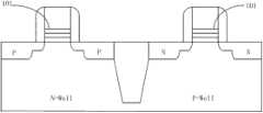
在采用高K金属栅极工艺的元件的虚设栅极形成过程中,在高K材料层上沉积的TiN膜会和多晶硅发生反应生成TiON或TiO2,如图1中101所示,在随后进行的干刻蚀或湿刻蚀步骤中很难将之去除。而TiON或TiO2层的存在会对半导体元件的门限电压(Vt)产生极大的影响。During the formation of the dummy gate of the element using the high-K metal gate process, the TiN film deposited on the high-K material layer will react with polysilicon to form TiON or TiO2, as shown by 101 in Figure 1, and the subsequent It is difficult to remove it in dry etching or wet etching steps. However, the existence of the TiON or TiO2 layer will have a great influence on the threshold voltage (Vt) of the semiconductor element.
但是目前的高K金属栅工艺中没有方法来克服上述问题。However, there is no way to overcome the above-mentioned problems in the current high-K metal gate technology.
发明内容Contents of the invention
鉴于以上问题,本发明提供一种采用高K金属栅极工艺的半导体制造方法,特别是用于Gate First的制造过程中,避免TiN与多晶硅发生反应产生TiON或TiO2,从而能够对半导体元件的门限电压进行较好地控制。In view of the above problems, the present invention provides a semiconductor manufacturing method using a high-K metal gate process, especially in the manufacturing process of Gate First, to avoid the reaction of TiN and polysilicon to produce TiON or TiO2, so that the threshold of the semiconductor element can be adjusted. Voltage is better controlled.
本发明包括以下步骤:提供一衬底;在所述衬底上形成栅堆栈层,包括依次层叠的高K介电层、TiN覆盖层、多晶硅层,以及位于所述TiN覆盖层和多晶硅层之间的阻挡层;蚀刻所述栅堆栈层以在所述衬底上形成虚设栅极结构;在所述衬底中形成源漏极;去除所述虚设栅极结构的所述多晶硅层;在所述阻挡层形成金属栅极。The invention includes the following steps: providing a substrate; forming a gate stack layer on the substrate, including a high-K dielectric layer, a TiN capping layer, a polysilicon layer stacked in sequence, and a gate stack layer located between the TiN capping layer and the polysilicon layer barrier layer between; etching the gate stack layer to form a dummy gate structure on the substrate; forming source and drain in the substrate; removing the polysilicon layer of the dummy gate structure; The blocking layer forms a metal gate.
进一步,所述阻挡层为TaN或AlN层。Further, the barrier layer is a TaN or AlN layer.
进一步,所述阻挡层具有10-50埃的厚度。Further, the barrier layer has a thickness of 10-50 angstroms.
进一步,还包括在所述衬底和所述栅堆栈层之间形成界面层。Further, it also includes forming an interface layer between the substrate and the gate stack layer.
进一步,所述界面层为氧化硅。Further, the interface layer is silicon oxide.
进一步,所述半导体器件为PMOS,所述阻挡层的厚度为10-30埃。Further, the semiconductor device is PMOS, and the barrier layer has a thickness of 10-30 angstroms.
进一步,所述半导体器件为NMOS,所述阻挡层的厚度为5-20埃。Further, the semiconductor device is NMOS, and the barrier layer has a thickness of 5-20 angstroms.
进一步,其中e)步骤去除虚设栅极结构中的多晶硅层使用的气体包括HBr、02、Ar。Further, the gas used in step e) to remove the polysilicon layer in the dummy gate structure includes HBr, O 2 , and Ar.
进一步,其中f)步骤中形成的金属栅极包括依次层叠的功函数金属层、阻挡层和导电层。Further, the metal gate formed in step f) includes a work function metal layer, a barrier layer and a conductive layer stacked in sequence.
进一步,所述半导体器件为PMOS,其中功函数金属层包括一层或多层TiN、TaN、Ta或其组合。Further, the semiconductor device is a PMOS, wherein the work function metal layer includes one or more layers of TiN, TaN, Ta or a combination thereof.
进一步,所述半导体器件为NMOS,其中功函数金属层包括一层或多层TiAl、Ti和Al、TiN和Al或其组合。Further, the semiconductor device is NMOS, wherein the work function metal layer includes one or more layers of TiAl, Ti and Al, TiN and Al or a combination thereof.
进一步,其中功函数金属层具有10-200埃的厚度。Further, the work function metal layer has a thickness of 10-200 angstroms.
进一步,其中功函数金属层的形成方法是ALD或PVD或CVD。Further, the method for forming the work function metal layer is ALD, PVD or CVD.
进一步,其中金属栅极的所述阻挡层选自TaN、TiN、Ta及其组合。Further, the barrier layer of the metal gate is selected from TaN, TiN, Ta and combinations thereof.
进一步,其中金属栅极的所述阻挡层具有10-100埃的厚度。Further, the barrier layer of the metal gate has a thickness of 10-100 angstroms.
进一步,其中金属栅极的所述阻挡层的形成方法是ALD或PVD。Further, the formation method of the barrier layer of the metal gate is ALD or PVD.
进一步,其中所述导电层包括Al。Further, the conductive layer includes Al.
进一步,其中所述导电层的形成方法是CVD或PVD。Further, the method for forming the conductive layer is CVD or PVD.
进一步,还包括在氮气中对所述金属栅极进行退火的步骤,其中退火的温度是300-500摄氏度,时间是10-60分钟。Further, it also includes the step of annealing the metal gate in nitrogen, wherein the annealing temperature is 300-500 degrees Celsius, and the time is 10-60 minutes.
本发明可以解决半导体制造过程不能很好地控制门限电压的技术问题。在制造NMOS和PMOS时,可以分别对阻挡层的厚度作出选择来控制门限电压。The invention can solve the technical problem that the threshold voltage cannot be well controlled in the semiconductor manufacturing process. When manufacturing NMOS and PMOS, the thickness of the barrier layer can be selected separately to control the threshold voltage.
附图说明Description of drawings
图1是采用现有高K金属栅极工艺所形成半导体栅极的结构示意图;FIG. 1 is a schematic structural diagram of a semiconductor gate formed by using an existing high-K metal gate process;
图2A-2G是本发明各个工艺步骤的器件剖面图。2A-2G are device cross-sectional views of various process steps of the present invention.
具体实施方式Detailed ways
在下文的描述中,给出了大量具体的细节以便提供对本发明更为彻底的理解。然而,对于本领域技术人员而言显而易见的是,本发明可以无需一个或多个这些细节而得以实施。在其他的例子中,为了避免与本发明发生混淆,对于本领域公知的一些技术特征未进行描述。为了彻底理解本发明,将在下列的描述中提出详细的步骤,以便阐释本发明提出的高K金属栅极工艺的半导体制造方法。显然,本发明的施行并不限定于半导体领域的技术人员所熟习的特殊细节。本发明的较佳实施例详细描述如下,然而除了这些详细描述外,本发明还可以具有其他实施方式。In the following description, numerous specific details are given in order to provide a more thorough understanding of the present invention. It will be apparent, however, to one skilled in the art that the present invention may be practiced without one or more of these details. In other examples, some technical features known in the art are not described in order to avoid confusion with the present invention. In order to thoroughly understand the present invention, detailed steps will be provided in the following description to explain the semiconductor manufacturing method of the high-K metal gate process proposed by the present invention. Obviously, the practice of the invention is not limited to specific details familiar to those skilled in the semiconductor arts. Preferred embodiments of the present invention are described in detail below, however, the present invention may have other embodiments besides these detailed descriptions.
应当理解的是,当在本说明书中使用术语“包含”和/或“包括”时,其指明存在所述特征、整体、步骤、操作、元件和/或组件,但不排除存在或附加一个或多个其他特征、整体、步骤、操作、元件、组件和/或它们的组合接下来,将结合附图更加完整地描述本发明。It should be understood that when the terms "comprising" and/or "comprising" are used in this specification, they indicate the presence of the features, integers, steps, operations, elements and/or components, but do not exclude the presence or addition of one or A number of other features, wholes, steps, operations, elements, components and/or combinations thereof Next, the present invention will be described more fully with reference to the accompanying drawings.
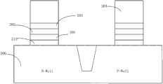
首先,如图2A所示,提供一衬底200。所述衬底可以为以下所提到的材料中的至少一种:硅、绝缘体上硅(SOI)、绝缘体上层叠硅(SSOI)、绝缘体上层叠锗化硅(S-SiGeOI)以及绝缘体上锗化硅(SiGeOI)等。在所述衬底中可以形成有掺杂区域和/或隔离结构,所述隔离结构为浅沟槽隔离(STI)结构或者局部氧化硅(LOCOS)隔离结构。在本发明的实施例中,所述衬底可以是Si衬底,其还可以包括在Si上的SiO2界面层210,通过快速热氧化工艺(RTO)或原子层沉积工艺(ALD)来形成SiO2界面层。然后在该衬底上形成栅极介电层201,可以选用高K材料来形成所述栅极介电层,例如用在Hf02中引入Si、Al、N、La、Ta等元素并优化各元素的比率来得到的高K材料等。所述形成栅极介电层的方法可以是物理气相沉积工艺或原子层沉积工艺。在本发明的实施例中,在所述SiO2界面层上形成HfAION栅极介电层,其厚度为15到60埃。之后,在栅极介电层201上形成栅极堆栈结构的TiN覆盖层202,然后在TiN层202上沉积扩散阻挡层203,可以是TaN层或AlN层。所述沉积扩散阻挡层的方法可以是原子层沉积法(ALD),物理气相沉积法(PVD),化学气相沉积法(CVD)等方法。在本发明的一个实施例中,在UHV/CVD反应腔中进行所述TaN层或AlN层203的沉积,所选择的工艺条件包括压强为1-100乇,温度为500-1000摄氏度。所沉积的TaN层或AlN层203具有10-50埃的厚度。之后在扩散阻挡层203上沉积包括多晶硅材料的栅极电极层204。在本发明的一个实施例中,使用低压化学气相淀积(LPCVD)工艺来形成多晶硅的栅极电极层,其的工艺条件包括:反应气体为硅烷(SiH4),所述硅烷的流量范围为100~200立方厘米/分钟(sccm),如150sccm;反应腔内温度范围为700~750摄氏度;反应腔内压力为250~350毫毫米汞柱(mTorr),如300mTorr;所述反应气体中还包括缓冲气体,所述缓冲气体可为氦气(He)或氮气,所述氦气和氮气的流量范围为5~20升/分钟(slm),如8slm、10slm或15slm。First, as shown in FIG. 2A , a
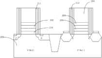
然后,如图2B所示,进行形成栅极的步骤。可以使用光刻工艺对以上步骤所形成的SiO2界面层210,栅极介电层201.TiN层202和TaN层或AlN层203、栅极电极层204进行图案化处理。所形成的栅极具有堆栈的结构。Then, as shown in FIG. 2B, a step of forming a gate is performed. The
然后,如图2C所示,进行形成偏移侧墙(offset spacer)211的步骤。偏移侧墙的材料可以是氮化硅,氧化硅或者氮氧化硅等绝缘材料。偏移侧墙可以提高形成的晶体管的沟道长度,减小短沟道效应和由于短沟道效应引起的热载流子效应。形成偏移侧墙的工艺可以是化学气相沉积。在一个实施例中所形成的偏移侧墙的厚度可以小到80埃。Then, as shown in FIG. 2C , a step of forming an offset
接着,形成轻掺杂源极/漏极(LDD)于栅极结构任一侧的衬底中。所述形成LDD的方法可以是离子注入工艺或扩散工艺。所述LDD注入的离子类型根据将要形成的半导体器件的电性决定,即形成的器件为NMOS器件,则LDD注入工艺中掺入的杂质离子为磷、砷、锑、铋中的一种或组合;若形成的器件为PMOS器件,则注入的杂质离子为硼。根据所需的杂质离子的浓度,离子注入工艺可以一步或多步完成。Next, lightly doped source/drain (LDD) is formed in the substrate on either side of the gate structure. The method for forming the LDD may be an ion implantation process or a diffusion process. The ion type of the LDD implantation is determined according to the electrical properties of the semiconductor device to be formed, that is, the formed device is an NMOS device, and the impurity ions doped in the LDD implantation process are one or a combination of phosphorus, arsenic, antimony, and bismuth ; If the formed device is a PMOS device, the implanted impurity ions are boron. Depending on the desired concentration of impurity ions, the ion implantation process can be performed in one or more steps.
然后,在衬底200和上述步骤所形成的偏移侧墙上形成间隙壁(Spacer)212,可以使用氮化硅、碳化硅、氮氧化硅或其组合的材料。可以在衬底上沉积第一氧化硅层、第一氮化硅层以及第二氧化硅层,然后采用蚀刻方法形成间隙壁,所述间隙壁可以具有10-30NM的厚度。Then, a spacer (Spacer) 212 is formed on the
然后,用离子注入工艺或扩散工艺重掺杂源极和漏极(S/D)形成于栅极间隙壁任一侧的衬底中。Then, heavily doped source and drain (S/D) electrodes are formed in the substrate on either side of the gate spacer by an ion implantation process or a diffusion process.
还可以包括退火步骤、形成袋形注入区、NiSi沉积等步骤。It may also include an annealing step, forming a pocket implant region, NiSi deposition and other steps.
然后在器件表面形成金属硅化物(SAB)阻挡层,可以使用TEOS与氧气形成氧化膜作为SAB膜,然后通过光刻和干刻来形成SAB区。优选的,还可以在形成的SAB膜之前先沉积SiN膜以消除在SAB膜光刻和刻蚀中对会侧墙刻蚀掉的影响。Then a metal silicide (SAB) barrier layer is formed on the surface of the device, an oxide film can be formed using TEOS and oxygen as the SAB film, and then the SAB region is formed by photolithography and dry etching. Preferably, a SiN film may be deposited before the SAB film is formed to eliminate the influence of sidewall etching during the photolithography and etching of the SAB film.
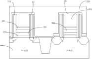
然后,参照图2D,在表面沉积蚀刻停止层221蚀刻停止层可用SiCN、SiN、SiC、SiOF、SiON等形成.然后进行沉积层间介电层(ILD)220于栅极结构上。可以采用化学气相沉积法、高密度等离子体化学气相沉积法、旋转涂布法、溅镀等方法形成。所述层间介电层可以采用氧化硅、氮氧化硅、氮化硅等材料。Then, referring to FIG. 2D, an
然后,参照图2E,对层间介电层220和以上步骤中沉积的层间介电层进行平坦化处理。所述平坦化处理的非限制性实例包括机械平坦化方法和化学机械抛光平坦化方法。以暴露栅极结构的上表面并使其大致与层间介电层220位于一个平面上。Then, referring to FIG. 2E , the
接着,去除PMOS的虚设栅极,形成沟槽300。所述去除的方法可以是光刻和蚀刻。在蚀刻过程中所用的气体包括HBr,其作为主要蚀刻气体;还包括作为刻蚀补充气体的02或Ar,其可以提高刻蚀的品质。在该步骤之后,PMOS中的TaN或AlN层203的最终厚度在10-30埃之间。Next, the dummy gate of the PMOS is removed to form the
然后,参照图2F,进行形成PMOS金属栅极301的步骤。所述金属栅极通过沉积多个薄膜堆栈形成。所述薄膜包括功函数金属层,阻挡层和导电层。所述阻挡层包括TaN、TiN、TaC、TaSiN、WN、TiAl、TiAlN或上述的组合。所述沉积阻挡层方法非限制性实例包括化学气相沉积法(CVD),如低温化学气相沉积(LTCVD)、低压化学气相沉积(LPCVD)、快热化学气相沉积(LTCVD)、等离子体化学气相沉积(PECVD)。在本发明的一个实施例中使用原子层沉积(ALD)、溅镀及物理气相沉积(PVD)的方法,所形成的阻挡层的厚度在10-100埃之间。所述功函数金属层包括一层或多层金属层。所述金属层可以是TiN、TaN、TiN和TaN、上述的组合。所述金属层可以用ALD、PVD或CVD的方法形成。优选地,所述功函数金属层的厚度在10-200埃之间。所述导电层可以是铝层,也可以是铜或钨层。在本发明的一个实施例中使用Al形成所述导电层,可以用CVD或PVD的方法进行沉积。在该导电层形成之后,在300-500摄氏度温度下进行退火。其在含氮环境中反应的时间为10-60分钟。最后进行导电层的平坦化,以除去沟槽300以外的导电层而形成PMOS金属栅极301。Then, referring to FIG. 2F , a step of forming a
然后,参考图2F,用光刻和蚀刻的方法进行NMOS的虚设栅极的去除形成沟槽400。在该步骤之后,NMOS中的TaN或AlN层203的最终厚度在5-20埃之间。Then, referring to FIG. 2F , the dummy gate of the NMOS is removed by photolithography and etching to form a trench 400 . After this step, the final thickness of the TaN or
然后,参照图2G,进行形成NMOS金属栅极401的步骤。所述金属栅极通过沉积多个薄膜堆栈形成。所述薄膜包括功函数金属层,阻挡层和导电层。所述阻挡层包括TaN、TiN、TaC、TaSiN、WN、TiAl、TiAlN或上述的组合。所述沉积阻挡层方法非限制性实例包括化学气相沉积法(CVD),如低温化学气相沉积(LTCVD)、低压化学气相沉积(LPCVD)、快热化学气相沉积(LTCVD)、等离子体化学气相沉积(PECVD)。在本发明的一个实施例中使用原子层沉积(ALD)、溅镀及物理气相沉积(PVD)的方法,所形成的阻挡层的厚度在10-100埃之间。所述功函数金属层包括一层或多层金属层。所述金属层可以是TiAl、Ti和Al、TiN和Al、上述的组合。所述金属层可以用ALD、PVD或CVD的方法形成。优选地,所述功函数金属层的厚度在10-200埃之间。所述导电层可以是铝层,也可以是铜或钨层。在本发明的一个实施例中使用Al形成所述导电层,可以用CVD或PVD的方法进行沉积。在该导电层形成之后,在300-500摄氏度温度下进行退火。在环境氮中反应的时间为10-60分钟。最后进行导电层的平坦化,以除去沟槽400以外的导电层而形成NMOS金属栅极401。Then, referring to FIG. 2G , a step of forming an
在以上步骤中,观察到沉积的TaN或AlN在高温退火之后具有较高的结晶度;TaN或AlN层和TiN层中各自的密度变化仅分别为30%(9.16-12.13g/cc)和10%(4.64-5.08g/cc)。In the above steps, it was observed that the deposited TaN or AlN had high crystallinity after high-temperature annealing; the respective density changes in the TaN or AlN layer and the TiN layer were only 30% (9.16-12.13 g/cc) and 10 % (4.64-5.08g/cc).
所以用本发明的方法可以克服半导体制造过程中半导体制造过程中对门限电压造成较大影响的技术问题,除此之外,还可以对TaN或AlN层的厚度作出选择来控制门限电压。Therefore, the method of the present invention can overcome the technical problem that the threshold voltage is greatly affected in the semiconductor manufacturing process. In addition, the thickness of the TaN or AlN layer can also be selected to control the threshold voltage.
然后进行后续工艺以完成半导体元件的制造。Subsequent processes are then performed to complete the fabrication of the semiconductor element.
为了说明和描述的目的,给出了本发明各个方面的以上描述。其并不旨在穷尽列举或将本发明限制为所公开的精确形式,且明显地,可以进行多种修改和变化。本发明旨在将对本领域技术人员是显而易见的这些修改和变化包括在由所附权利要求限定的本发明的范围内。The foregoing description of various aspects of the invention has been presented for purposes of illustration and description. It is not intended to be exhaustive or to limit the invention to the precise form disclosed, and obviously many modifications and changes are possible. The present invention is intended to include within the scope of the present invention such modifications and variations as would be apparent to those skilled in the art.
Claims (19)
Priority Applications (1)
| Application Number | Priority Date | Filing Date | Title |
|---|---|---|---|
| CN2012101815797ACN103456614A (en) | 2012-06-04 | 2012-06-04 | Manufacturing method for semiconductor device with high-K metal gate |
Applications Claiming Priority (1)
| Application Number | Priority Date | Filing Date | Title |
|---|---|---|---|
| CN2012101815797ACN103456614A (en) | 2012-06-04 | 2012-06-04 | Manufacturing method for semiconductor device with high-K metal gate |
Publications (1)
| Publication Number | Publication Date |
|---|---|
| CN103456614Atrue CN103456614A (en) | 2013-12-18 |
Family
ID=49738863
Family Applications (1)
| Application Number | Title | Priority Date | Filing Date |
|---|---|---|---|
| CN2012101815797APendingCN103456614A (en) | 2012-06-04 | 2012-06-04 | Manufacturing method for semiconductor device with high-K metal gate |
Country Status (1)
| Country | Link |
|---|---|
| CN (1) | CN103456614A (en) |
Cited By (4)
| Publication number | Priority date | Publication date | Assignee | Title |
|---|---|---|---|---|
| CN110459468A (en)* | 2019-08-29 | 2019-11-15 | 上海华力集成电路制造有限公司 | The lithographic method of TiAlN thin film |
| WO2020209081A1 (en)* | 2019-04-11 | 2020-10-15 | 東京エレクトロン株式会社 | Film forming method, method for manufacturing semiconductor device, film forming device, and system for manufacturing semiconductor device |
| CN114530493A (en)* | 2020-11-23 | 2022-05-24 | 长鑫存储技术有限公司 | Semiconductor structure and method for manufacturing semiconductor structure |
| CN114628389A (en)* | 2020-12-10 | 2022-06-14 | 中国科学院微电子研究所 | Method for manufacturing semiconductor structure and semiconductor structure |
Citations (6)
| Publication number | Priority date | Publication date | Assignee | Title |
|---|---|---|---|---|
| US20100112798A1 (en)* | 2008-11-03 | 2010-05-06 | Taiwan Semiconductor Manufacturing Company, Ltd. | Method for gap filling in a gate last process |
| CN102024813A (en)* | 2009-09-14 | 2011-04-20 | 台湾积体电路制造股份有限公司 | Semiconductor device, CMOS device and integrated circuit |
| CN102280375A (en)* | 2010-06-08 | 2011-12-14 | 中国科学院微电子研究所 | A method for preparing a stacked metal gate structure in a gate-first process |
| CN102299061A (en)* | 2010-06-22 | 2011-12-28 | 中国科学院微电子研究所 | Method for manufacturing semiconductor device |
| CN102339752A (en)* | 2010-07-14 | 2012-02-01 | 中国科学院微电子研究所 | Method for manufacturing semiconductor device based on gate replacement process |
| CN102386081A (en)* | 2010-09-02 | 2012-03-21 | 中芯国际集成电路制造(上海)有限公司 | Method for forming metal gate |
- 2012
- 2012-06-04CNCN2012101815797Apatent/CN103456614A/enactivePending
Patent Citations (6)
| Publication number | Priority date | Publication date | Assignee | Title |
|---|---|---|---|---|
| US20100112798A1 (en)* | 2008-11-03 | 2010-05-06 | Taiwan Semiconductor Manufacturing Company, Ltd. | Method for gap filling in a gate last process |
| CN102024813A (en)* | 2009-09-14 | 2011-04-20 | 台湾积体电路制造股份有限公司 | Semiconductor device, CMOS device and integrated circuit |
| CN102280375A (en)* | 2010-06-08 | 2011-12-14 | 中国科学院微电子研究所 | A method for preparing a stacked metal gate structure in a gate-first process |
| CN102299061A (en)* | 2010-06-22 | 2011-12-28 | 中国科学院微电子研究所 | Method for manufacturing semiconductor device |
| CN102339752A (en)* | 2010-07-14 | 2012-02-01 | 中国科学院微电子研究所 | Method for manufacturing semiconductor device based on gate replacement process |
| CN102386081A (en)* | 2010-09-02 | 2012-03-21 | 中芯国际集成电路制造(上海)有限公司 | Method for forming metal gate |
Cited By (10)
| Publication number | Priority date | Publication date | Assignee | Title |
|---|---|---|---|---|
| WO2020209081A1 (en)* | 2019-04-11 | 2020-10-15 | 東京エレクトロン株式会社 | Film forming method, method for manufacturing semiconductor device, film forming device, and system for manufacturing semiconductor device |
| JP2020172688A (en)* | 2019-04-11 | 2020-10-22 | 東京エレクトロン株式会社 | Deposition method, method for producing semiconductor device, deposition device, and system for producing semiconductor device |
| KR20210148279A (en)* | 2019-04-11 | 2021-12-07 | 도쿄엘렉트론가부시키가이샤 | A film forming method, a semiconductor device manufacturing method, a film forming apparatus, and a system for manufacturing a semiconductor device |
| JP7169931B2 (en) | 2019-04-11 | 2022-11-11 | 東京エレクトロン株式会社 | Film forming method, semiconductor device manufacturing method, film forming apparatus, and semiconductor device manufacturing system |
| KR102650982B1 (en)* | 2019-04-11 | 2024-03-26 | 도쿄엘렉트론가부시키가이샤 | Film forming method, semiconductor device manufacturing method, film forming apparatus, and system for manufacturing semiconductor devices |
| US12119219B2 (en) | 2019-04-11 | 2024-10-15 | Tokyo Electron Limited | Film forming method, method for manufacturing semiconductor device, film forming device, and system for manufacturing semiconductor device |
| CN110459468A (en)* | 2019-08-29 | 2019-11-15 | 上海华力集成电路制造有限公司 | The lithographic method of TiAlN thin film |
| CN114530493A (en)* | 2020-11-23 | 2022-05-24 | 长鑫存储技术有限公司 | Semiconductor structure and method for manufacturing semiconductor structure |
| CN114530493B (en)* | 2020-11-23 | 2024-05-03 | 长鑫存储技术有限公司 | Semiconductor structure and manufacturing method thereof |
| CN114628389A (en)* | 2020-12-10 | 2022-06-14 | 中国科学院微电子研究所 | Method for manufacturing semiconductor structure and semiconductor structure |
Similar Documents
| Publication | Publication Date | Title |
|---|---|---|
| JP5931312B2 (en) | CMOS semiconductor device and manufacturing method thereof | |
| CN102969347B (en) | The technology of metal gate device with more barrier layers is provided | |
| CN102194680B (en) | Fabrication method of gate structure | |
| US8765586B2 (en) | Methods of forming metal silicide regions on semiconductor devices | |
| WO2011079594A1 (en) | Semiconductor device and method of manufacturing the same | |
| CN102637685B (en) | Metal gate structure of a cmos semiconductor device | |
| CN102244098A (en) | Semiconductor device and method for manufacturing the same | |
| CN103579111B (en) | A kind of manufacture method of metal gate semiconductor device | |
| US20150084132A1 (en) | Silicon Nitride Layer Deposited at Low Temperature to Prevent Gate Dielectric Regrowth High-K Metal Gate Field Effect Transistors | |
| TW202027278A (en) | Semiconductor device and method manufacturing same | |
| CN103545186B (en) | A kind of method of manufacturing metal gate semiconductor devices | |
| CN106558482A (en) | A kind of semiconductor device and its manufacture method | |
| CN102956460B (en) | Method for manufacturing semiconductor element with metal gate | |
| CN103545185B (en) | A kind of method that use dummy grid manufactures semiconductor devices | |
| CN103456614A (en) | Manufacturing method for semiconductor device with high-K metal gate | |
| US20100193847A1 (en) | Metal gate transistor with barrier layer | |
| CN104681440A (en) | Semiconductor device and preparation method thereof | |
| CN107424926B (en) | Semiconductor device and manufacturing method thereof | |
| CN106328529B (en) | MOS transistor and forming method thereof | |
| CN103943492A (en) | Semiconductor device and preparation method thereof | |
| CN107240573B (en) | A semiconductor device and its manufacturing method and electronic device | |
| CN106558547B (en) | A kind of semiconductor device and its manufacturing method | |
| CN104051245B (en) | A kind of preparation method of semiconductor devices | |
| CN108511392B (en) | CMOS device and method for adjusting threshold of CMOS device | |
| TWI509702B (en) | Metal gate transistor and method for fabricating the same |
Legal Events
| Date | Code | Title | Description |
|---|---|---|---|
| C06 | Publication | ||
| PB01 | Publication | ||
| C10 | Entry into substantive examination | ||
| SE01 | Entry into force of request for substantive examination | ||
| RJ01 | Rejection of invention patent application after publication | Application publication date:20131218 | |
| RJ01 | Rejection of invention patent application after publication |