CN103454821A - Array substrate, flexible display device and electronic equipment - Google Patents
Array substrate, flexible display device and electronic equipmentDownload PDFInfo
- Publication number
- CN103454821A CN103454821ACN2013103977786ACN201310397778ACN103454821ACN 103454821 ACN103454821 ACN 103454821ACN 2013103977786 ACN2013103977786 ACN 2013103977786ACN 201310397778 ACN201310397778 ACN 201310397778ACN 103454821 ACN103454821 ACN 103454821A
- Authority
- CN
- China
- Prior art keywords
- line
- data line
- data
- lines
- array substrate
- Prior art date
- Legal status (The legal status is an assumption and is not a legal conclusion. Google has not performed a legal analysis and makes no representation as to the accuracy of the status listed.)
- Granted
Links
Images


Classifications
- G—PHYSICS
- G09—EDUCATION; CRYPTOGRAPHY; DISPLAY; ADVERTISING; SEALS
- G09G—ARRANGEMENTS OR CIRCUITS FOR CONTROL OF INDICATING DEVICES USING STATIC MEANS TO PRESENT VARIABLE INFORMATION
- G09G3/00—Control arrangements or circuits, of interest only in connection with visual indicators other than cathode-ray tubes
- G09G3/03—Control arrangements or circuits, of interest only in connection with visual indicators other than cathode-ray tubes specially adapted for displays having non-planar surfaces, e.g. curved displays
- G09G3/035—Control arrangements or circuits, of interest only in connection with visual indicators other than cathode-ray tubes specially adapted for displays having non-planar surfaces, e.g. curved displays for flexible display surfaces
- G—PHYSICS
- G02—OPTICS
- G02F—OPTICAL DEVICES OR ARRANGEMENTS FOR THE CONTROL OF LIGHT BY MODIFICATION OF THE OPTICAL PROPERTIES OF THE MEDIA OF THE ELEMENTS INVOLVED THEREIN; NON-LINEAR OPTICS; FREQUENCY-CHANGING OF LIGHT; OPTICAL LOGIC ELEMENTS; OPTICAL ANALOGUE/DIGITAL CONVERTERS
- G02F1/00—Devices or arrangements for the control of the intensity, colour, phase, polarisation or direction of light arriving from an independent light source, e.g. switching, gating or modulating; Non-linear optics
- G02F1/01—Devices or arrangements for the control of the intensity, colour, phase, polarisation or direction of light arriving from an independent light source, e.g. switching, gating or modulating; Non-linear optics for the control of the intensity, phase, polarisation or colour
- G02F1/13—Devices or arrangements for the control of the intensity, colour, phase, polarisation or direction of light arriving from an independent light source, e.g. switching, gating or modulating; Non-linear optics for the control of the intensity, phase, polarisation or colour based on liquid crystals, e.g. single liquid crystal display cells
- G02F1/133—Constructional arrangements; Operation of liquid crystal cells; Circuit arrangements
- G02F1/1333—Constructional arrangements; Manufacturing methods
- G02F1/133305—Flexible substrates, e.g. plastics, organic film
- G—PHYSICS
- G02—OPTICS
- G02F—OPTICAL DEVICES OR ARRANGEMENTS FOR THE CONTROL OF LIGHT BY MODIFICATION OF THE OPTICAL PROPERTIES OF THE MEDIA OF THE ELEMENTS INVOLVED THEREIN; NON-LINEAR OPTICS; FREQUENCY-CHANGING OF LIGHT; OPTICAL LOGIC ELEMENTS; OPTICAL ANALOGUE/DIGITAL CONVERTERS
- G02F1/00—Devices or arrangements for the control of the intensity, colour, phase, polarisation or direction of light arriving from an independent light source, e.g. switching, gating or modulating; Non-linear optics
- G02F1/01—Devices or arrangements for the control of the intensity, colour, phase, polarisation or direction of light arriving from an independent light source, e.g. switching, gating or modulating; Non-linear optics for the control of the intensity, phase, polarisation or colour
- G02F1/13—Devices or arrangements for the control of the intensity, colour, phase, polarisation or direction of light arriving from an independent light source, e.g. switching, gating or modulating; Non-linear optics for the control of the intensity, phase, polarisation or colour based on liquid crystals, e.g. single liquid crystal display cells
- G02F1/133—Constructional arrangements; Operation of liquid crystal cells; Circuit arrangements
- G02F1/1333—Constructional arrangements; Manufacturing methods
- G02F1/1343—Electrodes
- G02F1/134309—Electrodes characterised by their geometrical arrangement
- G02F1/134336—Matrix
- G—PHYSICS
- G09—EDUCATION; CRYPTOGRAPHY; DISPLAY; ADVERTISING; SEALS
- G09G—ARRANGEMENTS OR CIRCUITS FOR CONTROL OF INDICATING DEVICES USING STATIC MEANS TO PRESENT VARIABLE INFORMATION
- G09G3/00—Control arrangements or circuits, of interest only in connection with visual indicators other than cathode-ray tubes
- G09G3/20—Control arrangements or circuits, of interest only in connection with visual indicators other than cathode-ray tubes for presentation of an assembly of a number of characters, e.g. a page, by composing the assembly by combination of individual elements arranged in a matrix no fixed position being assigned to or needed to be assigned to the individual characters or partial characters
- G09G3/2092—Details of a display terminals using a flat panel, the details relating to the control arrangement of the display terminal and to the interfaces thereto
- G—PHYSICS
- G09—EDUCATION; CRYPTOGRAPHY; DISPLAY; ADVERTISING; SEALS
- G09G—ARRANGEMENTS OR CIRCUITS FOR CONTROL OF INDICATING DEVICES USING STATIC MEANS TO PRESENT VARIABLE INFORMATION
- G09G2300/00—Aspects of the constitution of display devices
- G09G2300/08—Active matrix structure, i.e. with use of active elements, inclusive of non-linear two terminal elements, in the pixels together with light emitting or modulating elements
- G09G2300/0809—Several active elements per pixel in active matrix panels
- G—PHYSICS
- G09—EDUCATION; CRYPTOGRAPHY; DISPLAY; ADVERTISING; SEALS
- G09G—ARRANGEMENTS OR CIRCUITS FOR CONTROL OF INDICATING DEVICES USING STATIC MEANS TO PRESENT VARIABLE INFORMATION
- G09G2320/00—Control of display operating conditions
- G09G2320/02—Improving the quality of display appearance
- G09G2320/0223—Compensation for problems related to R-C delay and attenuation in electrodes of matrix panels, e.g. in gate electrodes or on-substrate video signal electrodes
Landscapes
- Physics & Mathematics (AREA)
- Nonlinear Science (AREA)
- General Physics & Mathematics (AREA)
- Engineering & Computer Science (AREA)
- Mathematical Physics (AREA)
- Chemical & Material Sciences (AREA)
- Crystallography & Structural Chemistry (AREA)
- Optics & Photonics (AREA)
- Computer Hardware Design (AREA)
- Theoretical Computer Science (AREA)
- Geometry (AREA)
- Devices For Indicating Variable Information By Combining Individual Elements (AREA)
Abstract
Translated fromChineseDescription
Translated fromChinese技术领域technical field
本发明涉及柔性显示技术,特别是一种阵列基板、柔性显示器件及电子设备。The invention relates to flexible display technology, in particular to an array substrate, a flexible display device and electronic equipment.
背景技术Background technique
柔板显示(Flexible displays)是指一类使用柔性基板,可以制造成超薄、超大、可弯曲的显示器件或显示技术。柔性显示的最主要特点可以用三个字来描述:薄、轻、柔。Flexible displays refer to a class of flexible substrates that can be manufactured into ultra-thin, ultra-large, bendable display devices or display technologies. The main features of flexible displays can be described in three words: thin, light, and soft.
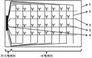
现有技术的柔性基板一般分为两个区域:一部分是非弯折区域,一部分是可弯折区域,如图1所示,阵列基板1其中在设置驱动模块4的位置为不可弯折区,该驱动模块4与数据线2以及栅线3连接,来驱动面板中设置的薄膜晶体管TFT5。The flexible substrate in the prior art is generally divided into two regions: one part is a non-bending region, and the other is a bendable region. As shown in FIG. The driving module 4 is connected to the
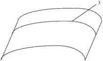
如图1所示,现有技术中,数据线2以及栅线3是以垂直于柔性基板的一个侧边的方式而设置。这种情况下,如图2所示,当显示器件以图2所示的方式弯折时,其中的栅线3会以图2所示的方式弯折。As shown in FIG. 1 , in the prior art, the
虽然现有技术,形成栅线的金属具有一定的拉伸性能,但当弯折超过一定程度时,容易导致栅线断裂,造成设备损坏。如果从材料方面入手,高拉伸性能的金属价格较高,会从整体上提高器件成本。Although in the prior art, the metal forming the grid lines has a certain tensile property, but when the bending exceeds a certain degree, the grid lines are likely to be broken and the equipment is damaged. If we start from the material aspect, the price of metal with high tensile properties is higher, which will increase the cost of the device as a whole.
发明内容Contents of the invention
本发明实施例的目的在于提供一种阵列基板、柔性显示器件及电子设备,在不增加器件成本的情况下提高柔性显示基板的弯折能力。The purpose of the embodiments of the present invention is to provide an array substrate, a flexible display device and an electronic device, which can improve the bending ability of the flexible display substrate without increasing the cost of the device.
为了实现上述目的,本发明实施例提供了一种阵列基板,包括柔性基板和在柔性基板上形成的阵列层,所述阵列层包括:In order to achieve the above object, an embodiment of the present invention provides an array substrate, including a flexible substrate and an array layer formed on the flexible substrate, and the array layer includes:
信号传输线,包括多条数据线和多条栅线,相互交叉在所述柔性基板上形成多个子像素区;Signal transmission lines, including a plurality of data lines and a plurality of gate lines, intersect with each other to form a plurality of sub-pixel regions on the flexible substrate;
设置于所述子像素区中的薄膜晶体管,与对应的数据线和栅线连接;The thin film transistor disposed in the sub-pixel area is connected to the corresponding data line and gate line;
至少一部分所述信号传输线相对于所述柔性基板的任意一个侧边的夹角不等于90度。An included angle of at least a part of the signal transmission lines with respect to any side of the flexible substrate is not equal to 90 degrees.
上述的阵列基板,其中,所述数据线和栅线相互垂直,且数据线与所述柔性基板的一个侧边的夹角在30度到60度之间。In the above-mentioned array substrate, the data lines and the gate lines are perpendicular to each other, and the included angle between the data lines and one side of the flexible substrate is between 30 degrees and 60 degrees.
上述的阵列基板,其中,数据线与所述柔性基板的一个侧边的夹角为45度。In the above array substrate, the angle between the data line and one side of the flexible substrate is 45 degrees.
上述的阵列基板,其中,所述多条数据线包括与第一数量的薄膜晶体管连接的第一数据线和与第二数量的薄膜晶体管连接的第二数据线。In the above array substrate, the plurality of data lines include first data lines connected to a first number of thin film transistors and second data lines connected to a second number of thin film transistors.
上述的阵列基板,其中,所述阵列基板还包括驱动模块,所述驱动模块向第一数据线输出的数据驱动信号中子信号的数量为第一数量,所述驱动模块向第二数据线输出的数据驱动信号中子信号的数量为第二数量。The above-mentioned array substrate, wherein, the array substrate further includes a driving module, the number of sub-signals in the data driving signal output by the driving module to the first data line is the first number, and the driving module outputs to the second data line The number of sub-signals in the data driving signal is the second number.
上述的阵列基板,其中,所述多条数据线存在第一数据线和长度大于第一数据线的长度的第二数据线;和/或The above-mentioned array substrate, wherein the plurality of data lines includes a first data line and a second data line whose length is greater than that of the first data line; and/or
所述多条栅线存在第一栅线和长度大于第一栅线的长度的第二栅线。The plurality of gate lines includes a first gate line and a second gate line whose length is greater than that of the first gate line.
上述的阵列基板,其中,所述第二数据线的截面面积大于所述第一数据线的截面面积,使得截面面积不同的第一数据线与第二数据线之间的第一传输时延差小于截面面积相同的第一数据线与第二数据线之间的第二传输时延差;The above-mentioned array substrate, wherein, the cross-sectional area of the second data line is larger than the cross-sectional area of the first data line, so that the first transmission delay difference between the first data line and the second data line with different cross-sectional areas less than the second transmission delay difference between the first data line and the second data line with the same cross-sectional area;
所述第二栅线的截面面积大于所述第一栅线的截面面积,使得截面面积不同的第一栅线与第二栅线之间的第三传输时延差小于截面面积相同的第一栅线与第二栅线之间的第四传输时延差。The cross-sectional area of the second gate line is larger than the cross-sectional area of the first gate line, so that the third transmission delay difference between the first gate line with different cross-sectional area and the second gate line is smaller than that of the first gate line with the same cross-sectional area. The fourth transmission delay difference between the gate line and the second gate line.
上述的阵列基板,其中,所述柔性基板划分为可弯折的显示区和不可弯折的外围区,所述阵列基板还包括设置于所述外围区的驱动模块。In the above array substrate, the flexible substrate is divided into a bendable display area and a non-bendable peripheral area, and the array substrate further includes a driving module disposed in the peripheral area.
上述的阵列基板,其中,所述驱动模块包括对应设置于所述柔性基板的相对的两个侧边的第一驱动模块和第二驱动模块,所述第一驱动模块和第二驱动模块以就近连接的原则与所述数据线和栅线连接。The above-mentioned array substrate, wherein, the driving module includes a first driving module and a second driving module correspondingly disposed on two opposite sides of the flexible substrate, and the first driving module and the second driving module are arranged in close proximity The connection principle is connected with the data line and the gate line.
为了实现上述目的,本发明实施例还提供了一种柔性显示器件,包括上述任意的阵列基板。In order to achieve the above purpose, an embodiment of the present invention further provides a flexible display device, including any of the above array substrates.
为了实现上述目的,本发明实施例还提供了一种电子设备,包括上述的柔性显示器件。In order to achieve the above object, an embodiment of the present invention further provides an electronic device, including the above flexible display device.
本发明实施例至少具有如下有益效果:Embodiments of the present invention have at least the following beneficial effects:
本发明实施例中,至少一部分所述信号传输线相对于柔性基板的一个侧边斜向设置,因此降低了基板弯折情况下信号传输线的弯曲程度,因此改善了基板的弯曲性能。In the embodiment of the present invention, at least a part of the signal transmission lines is arranged obliquely relative to one side of the flexible substrate, thereby reducing the degree of bending of the signal transmission lines when the substrate is bent, thereby improving the bending performance of the substrate.
附图说明Description of drawings
图1表示现有技术的柔性阵列基板的结构示意图;FIG. 1 shows a schematic structural view of a flexible array substrate in the prior art;
图2表示现有技术的柔性阵列基板弯折时信号传输线的弯曲情况示意图;FIG. 2 shows a schematic diagram of the bending of the signal transmission line when the flexible array substrate in the prior art is bent;
图3a-3b表示本发明实施例的信号传输线与柔性基板侧边夹角的示意图;3a-3b show schematic diagrams of the angle between the signal transmission line and the side of the flexible substrate according to the embodiment of the present invention;
图4a-4b表示本发明实施例的两种阵列基板的结构示意图;4a-4b show schematic structural diagrams of two array substrates according to an embodiment of the present invention;
图5为本发明实施例的阵列基板的效果比较示意图;FIG. 5 is a schematic diagram of comparing effects of array substrates according to an embodiment of the present invention;
图6为本发明实施例的设置有两个驱动模块的阵列基板的结构示意图;6 is a schematic structural diagram of an array substrate provided with two driving modules according to an embodiment of the present invention;
图7为本发明实施例的设置有两个驱动模块时就近连接的示意图;Fig. 7 is a schematic diagram of nearby connections when two drive modules are provided in an embodiment of the present invention;
图8表示本发明实施例的柔性阵列基板中不同数据线连接的薄膜晶体管的数量不同的示意图;FIG. 8 is a schematic diagram showing different numbers of thin film transistors connected to different data lines in a flexible array substrate according to an embodiment of the present invention;
图9表示本发明实施例的柔性阵列基板的数据线划分为两部分的示意图;FIG. 9 shows a schematic diagram of dividing the data line of the flexible array substrate into two parts according to the embodiment of the present invention;
图10为本发明实施例的数据驱动信号的时序示意图;FIG. 10 is a schematic timing diagram of a data driving signal according to an embodiment of the present invention;
图11为本发明实施例中形成的厚度不一的金属薄膜层的结构示意图;11 is a schematic structural view of metal thin film layers with different thicknesses formed in the embodiment of the present invention;
图12为本发明实施例中利用图11的金属薄膜层形成的厚度不一的信号传输线的结构示意图。FIG. 12 is a schematic structural diagram of signal transmission lines with different thicknesses formed by using the metal thin film layer in FIG. 11 in an embodiment of the present invention.
具体实施方式Detailed ways
本发明实施例的阵列基板、柔性显示器件及电子设备中,一部分信号传输线相对于所述柔性基板的一个侧边斜向设置,因此,相对于现有技术的垂直于柔性阵列基板的侧边的布置方式,当柔性阵列基板弯折时,这些斜向布置的信号传输线的弯曲半径更大,也就是说,在相同的弯折情形下,本发明实施例的阵列基板中的信号传输线的弯折程度相对较小,所以提高了阵列基板的弯折能力。In the array substrate, flexible display device, and electronic equipment of the embodiments of the present invention, a part of the signal transmission line is arranged obliquely relative to one side of the flexible substrate. Arrangement mode, when the flexible array substrate is bent, the bending radius of these obliquely arranged signal transmission lines is larger, that is to say, under the same bending situation, the bending radius of the signal transmission lines in the array substrate of the embodiment of the present invention The extent is relatively small, so the bending ability of the array substrate is improved.
在本发明的具体实施例中,先对其中涉及到的线与线之间的夹角定义如下。In a specific embodiment of the present invention, the angle between the lines involved is defined as follows.
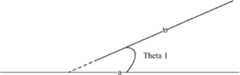
在本发明的具体实施例中,定义数据线与柔性基板的一个侧边的夹角的范围为[0,90度],均以显示区数据线和柔性基板侧边等效为直线(或线段)为例。解释如下。In a specific embodiment of the present invention, the range of the angle between the data line and one side of the flexible substrate is defined as [0, 90 degrees], and the data line in the display area and the side of the flexible substrate are equivalent to a straight line (or a line segment) ) as an example. The explanation is as follows.
如图3a所示,假定a为柔性基板的一个侧边,则信号传输线b和a的夹角定义为图3a中的Theta1,而图3b中,信号传输线b和a的夹角定义为图3b中的Theta2,当a和b垂直时,则a和b的夹角定位为90度,而a和b平行或重合时,a和b的夹角定位为0度。As shown in Figure 3a, assuming that a is a side of the flexible substrate, the angle between the signal transmission line b and a is defined as Theta1 in Figure 3a, and in Figure 3b, the angle between the signal transmission line b and a is defined as Figure 3b In Theta2, when a and b are perpendicular, the angle between a and b is positioned at 90 degrees, and when a and b are parallel or coincident, the angle between a and b is positioned at 0 degrees.
本发明实施例的一种阵列基板,如图4a-4e所示,包括柔性基板6和形成在柔性基板上的阵列层,阵列层包括显示区和非显示区,在显示区域内,所述阵列层包括:An array substrate according to an embodiment of the present invention, as shown in Figures 4a-4e, includes a
信号传输线,包括多条数据线2和多条栅线3,数据线2和栅线3相互交叉在所述柔性基板上形成多个子像素区;The signal transmission line includes a plurality of
设置于所述子像素区中的薄膜晶体管5,与对应的数据线2和栅线3连接;The thin film transistor 5 arranged in the sub-pixel area is connected to the
至少一部分所述信号传输线相对于所述柔性基板的任意一个侧边的夹角不等于90度。An included angle of at least a part of the signal transmission lines with respect to any side of the flexible substrate is not equal to 90 degrees.
如图4a所示,其中所有的栅线3与柔性基板的任意一个侧边的夹角都不等于90度,也就是说,栅线3与柔性基板的任意一个侧边的夹角Φ都满足如下的关系:0°<Φ<90°。As shown in Figure 4a, the included angles between all
可以理解的是,本发明实施例中是简化了薄膜晶体管5与数据线2、栅线3的结构关系;一般情况:薄膜晶体管5的栅极与栅线3连接,薄膜晶体管的源极(或漏极)与数据线2连接,薄膜晶体管的漏极(或源极)与像素电极(未示出)连接;由于薄膜晶体管的漏极和源极在制作工艺基本相同,可以在名称上互换。It can be understood that, in the embodiment of the present invention, the structural relationship between the thin film transistor 5 and the
当然,考虑到在柔性基板上必须有足够的像素点,因此,所述栅线3与柔性基板的侧边的夹角Φ取30°-60°之间为宜,在本发明的一个具体实施例中,该栅线3与柔性基板的侧边的夹角Φ取45°。Of course, considering that there must be enough pixels on the flexible substrate, it is advisable that the included angle Φ between the
图4a中,仅有栅线是斜向布置,但应当理解的是,数据线也可以是斜向布置,如图4b所示,其中所有的栅线3与柔性基板的任意一个侧边的夹角都不等于90度,也就是说,栅线3与柔性基板的任意一个侧边的夹角Φ都满足如下的关系:0°<Φ<90°。而同时,数据线2与柔性基板的任意一个侧边的夹角Ψ都满足如下的关系:0°<Ψ<90°。In Fig. 4a, only the gate lines are arranged obliquely, but it should be understood that the data lines may also be arranged obliquely, as shown in Fig. 4b, wherein all the
以图4b所示的结构中,在本发明的具体实施例中,可以设置数据线2和栅线3相互垂直,且数据线2与所述柔性基板的一个侧边的夹角在30度到60度之间。In the structure shown in Figure 4b, in a specific embodiment of the present invention, the
在本发明的一个具体实施例中,数据线与所述柔性基板的一个侧边的夹角为45度。In a specific embodiment of the present invention, the angle between the data line and one side of the flexible substrate is 45 degrees.
本发明实施例提及的线与线之间的角度关系,长度,数量的比较关系等,都是以在显示区域为例进行说明。下面对本发明实施例的斜向布置的信号传输线的弯折说明如下。The angle relationship between lines, the comparison relationship between length and quantity mentioned in the embodiment of the present invention are all described by taking the display area as an example. The following describes the bending of the obliquely arranged signal transmission lines in the embodiment of the present invention as follows.
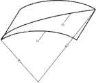
如图5所示,假定图5中,51为现有技术的垂直于柔性基板的一个侧边布置的第一信号传输线,而52为本发明实施例的相对于柔性基板的一个侧边斜向布置的第二信号传输线,从图中可以发现,由于第二信号传输线52的长度大于第一信号传输线51的长度,则在如图5所示的基板弯折情况下,第二信号传输线52具有比第一信号传输线51的曲率半径R1更大的曲率半径R2,也就是说,第二信号传输线52的弯曲程度比第一信号传输线51的弯曲程度要低。As shown in Figure 5, assume that in Figure 5, 51 is the first signal transmission line arranged perpendicular to one side of the flexible substrate in the prior art, and 52 is the oblique direction relative to one side of the flexible substrate in the embodiment of the present invention. The arranged second signal transmission line, it can be found from the figure that since the length of the second
按照几何原理,如果第二信号传输线52相对于柔性基板的一个侧边的夹角为45度,则第二信号传输线52的曲率半径大概是第二信号传输线51的曲率半径的1.4倍左右。According to the geometric principle, if the angle between the second
因此,本发明实施例通过相对于柔性基板的一个侧边斜向设置信号传输线,降低了基板弯折情况下,信号传输线的弯曲程度,因此改善了基板的弯曲性能。当然,本发明实施中以第二信号传输线与现有技术的第一信号传输线材质相同,且作用相同(例如都作为数据线)为例进行介绍,但并不以此为限。Therefore, the embodiment of the present invention reduces the bending degree of the signal transmission line when the substrate is bent by arranging the signal transmission line obliquely relative to one side of the flexible substrate, thereby improving the bending performance of the substrate. Certainly, in the implementation of the present invention, the material of the second signal transmission line is the same as that of the first signal transmission line in the prior art, and the function is the same (for example, they are both used as data lines) as an example for introduction, but it is not limited thereto.
在本发明的具体实施例中,为了保护驱动模块,可以将柔性基板划分为可弯折的显示区和不可弯折的外围区,并将驱动模块设置于所述外围区。In a specific embodiment of the present invention, in order to protect the driving module, the flexible substrate can be divided into a bendable display area and a non-bendable peripheral area, and the driving module is arranged in the peripheral area.
由于外围区的强度较大,因此相对于显示区弯折的可能性较小,将驱动模块设置于所述外围区能够提高对驱动模块的保护。Since the peripheral area has greater strength, it is less likely to be bent relative to the display area, and disposing the driving module in the peripheral area can improve the protection of the driving module.
在本发明的具体实施例中,所述驱动模块可以是一个,但也可以是两个或两个以上。以包括两个驱动模块为例,对应设置于所述柔性基板的相对的两个侧边,两个驱动模块以就近连接的原则与所述数据线和栅线连接。In a specific embodiment of the present invention, there may be one driving module, but there may also be two or more than two. Taking two drive modules as an example, they are arranged on two opposite sides of the flexible substrate, and the two drive modules are connected to the data lines and the gate lines on the principle of close connection.
包括有两个驱动模块的阵列基板如图6所示,可以发现,两个驱动模块以就近连接的原则与所述数据线和栅线连接。An array substrate including two driving modules is shown in FIG. 6 , and it can be found that the two driving modules are connected to the data line and the gate line in the principle of nearby connection.
下面以图7中的数据线2和栅线3对就近连接原则解释如下。Next, the principle of the connection of the
如图7所示,数据线2有可能通过第一连接线71连接到左边的驱动模块,也有可能通过第二连接线72连接到右边的驱动模块,但很明显,第一连接线的长度d1很明显会小于第二连接线72的长度d2,因此,按照就近连接原则,图7中的数据线2由左边的驱动模块进行驱动。As shown in Figure 7, the
如图7所示,栅线3有可能通过第三连接线73连接到右边的驱动模块,也有可能通过第四连接线74连接到左边的驱动模块,但很明显,第三连接线的长度d3很明显会小于第四连接线74的长度d4,因此,按照就近连接原则,图7中的栅线3由右边的驱动模块进行驱动。As shown in FIG. 7 , the
也就是说,对于任意一条信号传输线而言,按照就近连接原则,其到当前连接的驱动模块的连接距离会小于或等于其到另一驱动模块的最小连接距离。That is to say, for any signal transmission line, according to the principle of the nearest connection, the connection distance to the currently connected driving module will be less than or equal to the minimum connection distance to another driving module.
结合图6和图7所示,这种连接方式,大大降低了不同信号传输线与驱动模块之间的连接线的长度差异,也就降低了驱动模块发送的信号传输到不同信号传输线之间的传输时延,提高了系统性能。As shown in Figure 6 and Figure 7, this connection method greatly reduces the length difference between the connection lines between different signal transmission lines and the drive module, and also reduces the transmission of signals sent by the drive module to different signal transmission lines. time delay and improve system performance.
在上述的实施例中,上述的驱动模块同时驱动数据线和栅线,但应当理解的是,本发明实施例中的驱动模块也可以包括单独用于驱动数据线的数据驱动模块和单独用于驱动栅线的栅极驱动模块,该栅极驱动模块可以是独立存在的芯片,也可以是通过GOA(Gate on Array)方式集成于阵列基板。In the above-mentioned embodiment, the above-mentioned drive module drives the data line and the gate line at the same time, but it should be understood that the drive module in the embodiment of the present invention may also include a data drive module for driving the data line alone and a data drive module for A gate drive module for driving gate lines, which can be an independent chip or integrated on the array substrate through GOA (Gate on Array).
在本发明的具体实施例中,上述的数据线和/或栅线斜向设置之后,会使得至少有两条数据线具有不同的长度,和/或;至少两条栅线具有不同的长度;In a specific embodiment of the present invention, after the above-mentioned data lines and/or gate lines are arranged obliquely, at least two data lines have different lengths, and/or; at least two gate lines have different lengths;
进一步的,使得至少有两条数据线分别连接数量不同的薄膜晶体管,和/或,至少两条栅线分别连接数量不同的薄膜晶体管。Further, at least two data lines are respectively connected to different numbers of thin film transistors, and/or at least two gate lines are respectively connected to different numbers of thin film transistors.
例如:多条数据线中至少包括:与第一数量的薄膜晶体管连接的第一数据线,以及与第二数量的薄膜晶体管连接的第二数据线;For example: the plurality of data lines at least include: a first data line connected to a first number of thin film transistors, and a second data line connected to a second number of thin film transistors;
可以理解的是,“第一”和“第二”在比较数值关系时表示不相等,在相互位置关系是相对而言,并非特指。例如:第一数量不等于第二数量;图8所示,数据线81可以称为第一数据线,数据线82可以称为第二数据线,相对而言,数据线82可以称为第一数据线,数据线83可以称为第二数据线;此外,第一数据线(或第一栅线)可以是指其中一条数据线(或栅线),也可以指连接相同数量薄膜晶体管(或长度相同)等功能作用基本相同的数据线(或栅线)。It can be understood that "first" and "second" mean that they are not equal when comparing the numerical relationship, and the mutual positional relationship is relative and not specific. For example: the first number is not equal to the second number; as shown in FIG. 8, the
进一步的,所述驱动模块在一帧时间内向第一数据线输出的数据驱动信号中子信号的数量为第一数量,所述驱动模块在一帧时间内向第二数据线输出的数据驱动信号中子信号的数量为第二数量。Further, the number of sub-signals in the data driving signal output by the driving module to the first data line within one frame time is the first number, and the number of sub-signals in the data driving signal output by the driving module to the second data line within one frame time is The number of sub-signals is the second number.
子信号指的是驱动模块通过一个TFT输入到像素电极的信号。The sub-signal refers to a signal that the driving module inputs to the pixel electrode through a TFT.
以图8所示的情况为例,最上方的数据线81与7个TFT连接,而中间的数据线82与8个TFT连接,最下方的数据线83与9个TFT连接,此时,根据本发明实施例的阵列基板,在一帧时间内,驱动模块向最上方的数据线81输出的数据驱动信号中子信号的数量为7个,驱动模块向中间的数据线82输出的数据驱动信号中子信号的数量为8个,驱动模块向最下方的数据线83输出的数据驱动信号中子信号的数量为9个。Taking the situation shown in Figure 8 as an example, the
下面从驱动模块的角度来进一步描述如下。Further description is given below from the perspective of the drive module.
以图8所示的情况为例,最上方的数据线81与7个TFT连接,而中间的数据线82与8个TFT连接,最下方的数据线83与9个TFT连接;栅线811与1个TFT连接,栅线812与2个TFT连接,栅线813与3个TFT连接。此时,根据本发明实施例的阵列基板,栅线逐行扫描,在t1时间,驱动模块向栅线811输入栅极驱动信号,打开一个薄膜晶体管,此时驱动模块向数据线83输入数据驱动信号,则驱动模块输出的子信号数量为1个;同理,在t2时间,驱动模块向栅线812输入栅极驱动信号的子信号的数量为2个,此时驱动模块向数据线82、83输入数据驱动信号,则驱动模块输出的子信号数量为2个;以此类推……。Taking the situation shown in Figure 8 as an example, the
本发明实施例中,驱动模块根据数据线连接的薄膜晶体管的数量来决定数据驱动信号中子信号的数量,能够满足数据线连接的薄膜晶体管的数量不同的阵列基板的驱动需求,相对于现有技术具有更好的灵活性。In the embodiment of the present invention, the driving module determines the number of sub-signals in the data driving signal according to the number of thin film transistors connected to the data line, which can meet the driving requirements of array substrates with different numbers of thin film transistors connected to the data line. Technology has better flexibility.
如图9所示,在本发明的具体实施例中,按照所述数据线的排列方向,以柔性基板的对角线93为分割线,所述数据线分为第一部分91和第二部分92,位于所述柔性基板左上半部分的数据线为第一部分,位于所述柔性基板右下半部分的数据线为第二部分;As shown in Figure 9, in a specific embodiment of the present invention, according to the arrangement direction of the data lines, the
其中第一部分91所包括的数据线中,按照从上到下的顺序来看,在先的数据线连接的薄膜晶体管的数量小于在后的数据线连接的薄膜晶体管的数量;第二部分92所包括的数据线中,按照从上到下的顺序来看,在先的数据线连接的薄膜晶体管的数量大于在后的数据线连接的薄膜晶体管的数量。Among the data lines included in the
也就是说在数据线的排列方向上,数据线连接的晶体管数量先增大,后减小。That is to say, in the arrangement direction of the data lines, the number of transistors connected to the data lines first increases and then decreases.
优选的,数据线的排列方向上,数据线连接的晶体管数量先等差数值为P1增大,后按照等差数值为P2减小(P1和P2为大于等于1的正整数)。Preferably, in the arrangement direction of the data lines, the number of transistors connected to the data lines first increases with an arithmetic difference value of P1, and then decreases with an arithmetic difference value of P2 (P1 and P2 are positive integers greater than or equal to 1).
进一步的,等差数值为P1与P2相等,即数据线连接的晶体管数量相对对角线呈对称排列。例如P1=P2=2。Further, the arithmetic difference value is that P1 and P2 are equal, that is, the number of transistors connected to the data line is arranged symmetrically with respect to the diagonal line. For example P1=P2=2.
假定有2m条数据线,在数据线的排列方向上,依次连接的晶体管数量为:1、3、5、…、2n-3、2n-1、2n-1、2n-3、…、5、3、1(1≤n≤m,n,m均为正整数),则对应的本发明实施例的数据驱动信号如图10所示。Assuming that there are 2m data lines, in the arrangement direction of the data lines, the number of sequentially connected transistors is: 1, 3, 5, ..., 2n-3, 2n-1, 2n-1, 2n-3, ..., 5, 3. 1 (1≤n≤m, where n and m are both positive integers), the corresponding data driving signals of the embodiment of the present invention are shown in FIG. 10 .
从图10可以发现,在数据线的排列方向上,驱动模块发送的驱动信号包括的子信号的数量先是增大,然后减小。It can be found from FIG. 10 that, in the arrangement direction of the data lines, the number of sub-signals included in the driving signal sent by the driving module first increases and then decreases.
在本发明的具体实施例中,上述的数据线斜向设置之后,会导致多条数据线/栅线中,存在第一信号传输线,和长度大于第一信号传输线的长度的第二信号传输线,也就是说:In a specific embodiment of the present invention, after the above-mentioned data lines are arranged obliquely, there will be a first signal transmission line and a second signal transmission line whose length is greater than the length of the first signal transmission line among the multiple data lines/gate lines, That is to say:
存在第一栅线,和长度大于第一栅线的长度的第二栅线;和/或;there is a first gridline, and a second gridline having a length greater than the length of the first gridline; and/or;
第一数据线,和长度大于第一数据线的长度的第二数据线。a first data line, and a second data line whose length is greater than that of the first data line.
此时为了降低信号传输线之间的时延,本发明具体实施例中,所述第二信号传输线的截面面积大于所述第一信号传输线的截面面积,使得截面面积不同的第一信号传输线与第二信号传输线之间的第一传输时延差小于截面面积相同的第一信号传输线与第二信号传输线之间的第二传输时延差。At this time, in order to reduce the time delay between the signal transmission lines, in a specific embodiment of the present invention, the cross-sectional area of the second signal transmission line is larger than the cross-sectional area of the first signal transmission line, so that the first signal transmission line and the second signal transmission line with different cross-sectional areas The first transmission delay difference between the two signal transmission lines is smaller than the second transmission delay difference between the first signal transmission line and the second signal transmission line with the same cross-sectional area.
也就是说:That is to say:
所述第二数据线的截面面积大于所述第一数据线的截面面积,使得截面面积不同的第一数据线与第二数据线之间的第一传输时延差小于截面面积相同的第一数据线与第二数据线之间的第二传输时延差;The cross-sectional area of the second data line is larger than the cross-sectional area of the first data line, so that the first transmission delay difference between the first data line with different cross-sectional area and the second data line is smaller than that of the first data line with the same cross-sectional area. a second transmission delay difference between the data line and the second data line;
所述第二栅线的截面面积大于所述第一栅线的截面面积,使得截面面积不同的第一栅线与第二栅线之间的第三传输时延差小于截面面积相同的第一栅线与第二栅线之间的第四传输时延差。The cross-sectional area of the second gate line is larger than the cross-sectional area of the first gate line, so that the third transmission delay difference between the first gate line with different cross-sectional area and the second gate line is smaller than that of the first gate line with the same cross-sectional area. The fourth transmission delay difference between the gate line and the second gate line.
本发明实施例所述的阵列基板中,当存在长度不同的信号传输线时,根据二者长度的不同,在制作过程中控制生成的长度不同的信号传输线的截面面积,较长的信号传输线的截面面积较大,因此其阻抗效应相应减小,因此能够弥补由于其长度较长带来的时延,降低了不同信号传输线之间的时延差,提高了显示性能。In the array substrate described in the embodiment of the present invention, when there are signal transmission lines with different lengths, according to the difference in length between the two, the cross-sectional area of the signal transmission lines with different lengths generated during the production process is controlled, and the cross-sectional area of the longer signal transmission line The area is larger, so its impedance effect is correspondingly reduced, so it can make up for the time delay caused by its longer length, reduce the time delay difference between different signal transmission lines, and improve the display performance.
在本发明的具体实施例中,可以设置任意两条长度不同的数据线/栅线,长度较长的数据线/栅线的截面面积大于长度较短的数据线/栅线的截面面积。In a specific embodiment of the present invention, any two data lines/gate lines with different lengths can be provided, and the cross-sectional area of the longer data line/gate line is larger than that of the shorter data line/gate line.
在本发明的具体实施例中,为了保证第一信号传输线和第二信号传输线的截面面积不同,可以采用如下方式:In a specific embodiment of the present invention, in order to ensure that the cross-sectional areas of the first signal transmission line and the second signal transmission line are different, the following methods can be adopted:
截面厚度相同,第二信号传输线的截面宽度大于第一信号传输线的截面宽度;或者The cross-sectional thickness is the same, and the cross-sectional width of the second signal transmission line is larger than that of the first signal transmission line; or
截面宽度相同,第二信号传输线的截面厚度大于第一信号传输线的截面厚度;或者The cross-sectional width is the same, and the cross-sectional thickness of the second signal transmission line is greater than the cross-sectional thickness of the first signal transmission line; or
截面宽度和高度均不相同,第二信号传输线的截面宽度和高度的乘积大于第一信号传输线的截面宽度和高度的乘积。The cross-sectional width and height are different, and the product of the cross-sectional width and height of the second signal transmission line is greater than the product of the cross-sectional width and height of the first signal transmission line.
以信号传输线为数据线为例:数据线的排列方向上,数据线的截面面积可以呈等差或等比的关系先增大后减小;Take the signal transmission line as the data line as an example: in the arrangement direction of the data line, the cross-sectional area of the data line can first increase and then decrease in an equidifferential or proportional relationship;
进一步的,数据线的截面面积相对对角线呈对称排列。例如图11。Further, the cross-sectional area of the data line is arranged symmetrically with respect to the diagonal line. For example, Figure 11.
本发明实施例中,具有上述特征的阵列基板的制作方法包括:In an embodiment of the present invention, the manufacturing method of the array substrate having the above characteristics includes:
形成金属薄膜层;Forming a metal thin film layer;
对所述金属薄膜层进行蚀刻处理,形成多条数据线/栅线;Etching the metal thin film layer to form a plurality of data lines/gate lines;
其中,所述多条数据线/栅线中包括第一信号传输线和长度大于第一信号传输线的长度的第二信号传输线,所述第二信号传输线的截面面积大于所述第二信号传输线的截面面积。Wherein, the plurality of data lines/gate lines include a first signal transmission line and a second signal transmission line whose length is greater than that of the first signal transmission line, and the cross-sectional area of the second signal transmission line is greater than that of the second signal transmission line area.
在本发明的具体实施例中,任意两条长度不同的数据线/栅线,长度较长的数据线/栅线的截面面积大于长度较短的数据线/栅线的截面面积。In a specific embodiment of the present invention, for any two data lines/gate lines with different lengths, the cross-sectional area of the longer data line/gate line is larger than the cross-sectional area of the shorter data line/gate line.
按照上述的方式,结合图9所示,以数据线为例,在图9中箭头所示的方向上,数据线的长度先增大,后减小,按照本发明实施例的技术方案,如果在刻蚀过程中,每条数据线的宽度相同,则在数据线的排列方向上,数据线的厚度先增大,然后减小。According to the above method, as shown in FIG. 9, taking the data line as an example, in the direction indicated by the arrow in FIG. 9, the length of the data line first increases and then decreases. According to the technical solution of the embodiment of the present invention, if During the etching process, the width of each data line is the same, so in the arrangement direction of the data lines, the thickness of the data line first increases and then decreases.
在本发明的具体实施例中,所述形成金属薄膜层的步骤可以通过溅射工艺制作。In a specific embodiment of the present invention, the step of forming the metal thin film layer can be produced by a sputtering process.
上述的阵列基板的制作方法,其中,所述形成金属薄膜层的步骤具体包括:The above method for manufacturing an array substrate, wherein the step of forming the metal thin film layer specifically includes:
通过磁条形成一磁场,在待制作的数据线/栅线的排列方向上,所述磁场的磁场强度先变大后变小;A magnetic field is formed by the magnetic strip, and in the arrangement direction of the data line/gate line to be produced, the magnetic field strength of the magnetic field first becomes larger and then becomes smaller;
利用被电场加速后的等离子化惰性气体撞击靶材,撞击出原子在所述磁场的作用下在面板的表面沉积形成所述金属薄膜层。The plasma inert gas accelerated by the electric field is used to collide with the target, and atoms are deposited on the surface of the panel under the action of the magnetic field to form the metal thin film layer.
本发明实施例中,通过在基板后面设置斜向的磁条,其排列方向与待形成的数据线的排列方向相同,通过磁条之间形成磁场,在强磁场的位置则等离子体密度高,则成膜厚度高。通过将基板背后的磁条斜向设置,这样就可以正好对应到玻璃基板上的膜厚规律,形成如图11所示的金属膜厚。In the embodiment of the present invention, by arranging oblique magnetic stripes behind the substrate, the arrangement direction of which is the same as that of the data lines to be formed, a magnetic field is formed between the magnetic stripes, and the plasma density is high at the position of the strong magnetic field. Then the film thickness is high. By arranging the magnetic strip behind the substrate obliquely, it can just correspond to the film thickness rule on the glass substrate, forming the metal film thickness as shown in Figure 11.
如图11所示,为上述工艺过程之后形成的金属薄膜层的剖面示意图,在数据线排列方向上,可以发现,形成的金属薄膜层111的厚度先增大,然后减小,呈对称排列。As shown in FIG. 11 , it is a schematic cross-sectional view of the metal thin film layer formed after the above process. In the direction of the arrangement of the data lines, it can be found that the thickness of the formed metal
其中,沉积形成的金属薄膜层,按照待制作的数据线/栅线的排列方向,分为两个部分;Wherein, the deposited metal thin film layer is divided into two parts according to the arrangement direction of the data lines/gate lines to be produced;
在所述数据线/栅线的排列方向上,其中一部分金属薄膜层的厚度逐渐增大,而另一部分金属薄膜层的厚度逐渐减小。In the arrangement direction of the data lines/gate lines, the thickness of a part of the metal thin film layer gradually increases, while the thickness of the other part of the metal thin film layer gradually decreases.
这种有规律的波浪形的成膜厚度,刻蚀完成后,可以实现如图12所示的效果,其中在长的走线上有比较厚的膜厚,在短的走线上有比较薄的膜厚,从而实现均一的信号延迟。This regular wave-shaped film thickness, after the etching is completed, can achieve the effect shown in Figure 12, in which there is a relatively thick film thickness on the long traces, and a relatively thin film thickness on the short traces. film thickness to achieve uniform signal delay.
当然,应当理解的是,上述的数据线/栅线也可以通过打印或其他的方式来实现,在本发明具体实施例中不做具体限定。Of course, it should be understood that the above-mentioned data lines/gate lines may also be realized by printing or other methods, which are not specifically limited in specific embodiments of the present invention.
本发明实施例还提供了一种柔性显示器件,包括上述任意的阵列基板。其中,阵列基板的结构以及工作原理同上述实施例,在此不再赘述。另外,柔性显示器件其他部分的结构可以参考现有技术,对此本文不再详细描述。该柔性显示器件可以为:液晶面板、电子纸、液晶电视、液晶显示器、数码相框、手机、平板电脑等具有任何显示功能的产品或部件。An embodiment of the present invention also provides a flexible display device, including any of the above array substrates. Wherein, the structure and working principle of the array substrate are the same as those of the above-mentioned embodiments, and will not be repeated here. In addition, the structure of other parts of the flexible display device can refer to the prior art, which will not be described in detail herein. The flexible display device may be any product or component with display functions such as liquid crystal panel, electronic paper, liquid crystal TV, liquid crystal display, digital photo frame, mobile phone, and tablet computer.
本发明实施例还提供了一种电子设备,包括上述的柔性显示器件。An embodiment of the present invention also provides an electronic device, including the above-mentioned flexible display device.
以上所述是本发明的优选实施方式,应当指出,对于本技术领域的普通技术人员来说,在不脱离本发明所述原理的前提下,还可以作出若干改进和润饰,这些改进和润饰也应视为本发明的保护范围。The above description is a preferred embodiment of the present invention, it should be pointed out that for those of ordinary skill in the art, without departing from the principle of the present invention, some improvements and modifications can also be made, and these improvements and modifications can also be made. It should be regarded as the protection scope of the present invention.
Claims (11)
Translated fromChinesePriority Applications (3)
| Application Number | Priority Date | Filing Date | Title |
|---|---|---|---|
| CN201310397778.6ACN103454821B (en) | 2013-09-04 | 2013-09-04 | A kind of array base palte, flexible display device and electronic equipment |
| US14/402,971US9472134B1 (en) | 2013-09-04 | 2014-04-08 | Array substrate and method for manufacturing the same, flexible display device and electronic product |
| PCT/CN2014/074890WO2015032198A1 (en) | 2013-09-04 | 2014-04-08 | Array substrate and manufacturing method therefor, flexible display, and electronic device |
Applications Claiming Priority (1)
| Application Number | Priority Date | Filing Date | Title |
|---|---|---|---|
| CN201310397778.6ACN103454821B (en) | 2013-09-04 | 2013-09-04 | A kind of array base palte, flexible display device and electronic equipment |
Publications (2)
| Publication Number | Publication Date |
|---|---|
| CN103454821Atrue CN103454821A (en) | 2013-12-18 |
| CN103454821B CN103454821B (en) | 2016-06-15 |
Family
ID=49737366
Family Applications (1)
| Application Number | Title | Priority Date | Filing Date |
|---|---|---|---|
| CN201310397778.6AActiveCN103454821B (en) | 2013-09-04 | 2013-09-04 | A kind of array base palte, flexible display device and electronic equipment |
Country Status (3)
| Country | Link |
|---|---|
| US (1) | US9472134B1 (en) |
| CN (1) | CN103454821B (en) |
| WO (1) | WO2015032198A1 (en) |
Cited By (13)
| Publication number | Priority date | Publication date | Assignee | Title |
|---|---|---|---|---|
| CN103730476A (en)* | 2013-12-27 | 2014-04-16 | 京东方科技集团股份有限公司 | Array substrate and display device |
| CN103926774A (en)* | 2014-04-02 | 2014-07-16 | 京东方科技集团股份有限公司 | Array substrate, flexible display device and electronic equipment |
| CN104090439A (en)* | 2014-06-27 | 2014-10-08 | 京东方科技集团股份有限公司 | Array substrate, driving method of array substrate, flexible display device and electronic device |
| WO2015032210A1 (en)* | 2013-09-04 | 2015-03-12 | 京东方科技集团股份有限公司 | Array substrate and driving method therefor, flexible display, and electronic device |
| WO2015032198A1 (en)* | 2013-09-04 | 2015-03-12 | 京东方科技集团股份有限公司 | Array substrate and manufacturing method therefor, flexible display, and electronic device |
| CN104916245A (en)* | 2014-03-13 | 2015-09-16 | 三星显示有限公司 | Display device |
| CN106340250A (en)* | 2016-07-28 | 2017-01-18 | 友达光电股份有限公司 | Display panel |
| CN106486500A (en)* | 2016-12-28 | 2017-03-08 | 京东方科技集团股份有限公司 | Flexible array substrate and its manufacture method, flexible display panels and display device |
| CN106783890A (en)* | 2017-02-07 | 2017-05-31 | 京东方科技集团股份有限公司 | A kind of array base palte and preparation method thereof, display device |
| CN106952607A (en)* | 2017-05-25 | 2017-07-14 | 京东方科技集团股份有限公司 | Display substrate, display panel and display device |
| CN108181769A (en)* | 2018-01-29 | 2018-06-19 | 武汉华星光电技术有限公司 | A kind of array substrate, display panel and electronic equipment |
| CN109345993A (en)* | 2018-09-18 | 2019-02-15 | 深圳华信嘉源科技有限公司 | A matrix display screen and display control method thereof |
| US10831074B2 (en) | 2018-01-29 | 2020-11-10 | Wuhan China Star Optoelectronics Technology Co., Ltd. | Array substrate, display panel, and electronic apparatus |
Families Citing this family (2)
| Publication number | Priority date | Publication date | Assignee | Title |
|---|---|---|---|---|
| KR102645817B1 (en)* | 2016-12-06 | 2024-03-08 | 한화로보틱스 주식회사 | Apparatus and method for managing behavior of robot |
| KR102484880B1 (en)* | 2018-06-08 | 2023-01-05 | 엘지디스플레이 주식회사 | Stretchable display device, panel driving circuit and the method of driving the same |
Citations (4)
| Publication number | Priority date | Publication date | Assignee | Title |
|---|---|---|---|---|
| JP2009069768A (en)* | 2007-09-18 | 2009-04-02 | Toshiba Matsushita Display Technology Co Ltd | Liquid crystal display device |
| CN101807582A (en)* | 2009-02-16 | 2010-08-18 | 元太科技工业股份有限公司 | Flexible pixel array substrate and flexible display |
| CN102156360A (en)* | 2009-11-23 | 2011-08-17 | 乐金显示有限公司 | Flexible display device and manufacturing method thereof |
| CN203519983U (en)* | 2013-09-04 | 2014-04-02 | 京东方科技集团股份有限公司 | Array substrate, flexible display device and electronic equipment |
Family Cites Families (9)
| Publication number | Priority date | Publication date | Assignee | Title |
|---|---|---|---|---|
| CN201536453U (en)* | 2009-09-24 | 2010-07-28 | 北京京东方光电科技有限公司 | Cof flexible circuit board |
| CN201765413U (en)* | 2010-09-16 | 2011-03-16 | 深圳市飞格达电子有限公司 | High performance liquid crystal module structure |
| CN202056680U (en)* | 2011-04-15 | 2011-11-30 | 郎应红 | Novel backlight structure |
| CN102637633B (en)* | 2011-06-17 | 2015-08-12 | 京东方科技集团股份有限公司 | A kind of manufacturing method of array base plate and system |
| TWI440186B (en)* | 2011-09-23 | 2014-06-01 | E Ink Holdings Inc | Driving substrate and display device using same |
| US9601557B2 (en)* | 2012-11-16 | 2017-03-21 | Apple Inc. | Flexible display |
| CN103454822B (en)* | 2013-09-04 | 2016-03-30 | 京东方科技集团股份有限公司 | Array base palte and driving method, flexible display device and electronic equipment |
| CN103456743B (en)* | 2013-09-04 | 2016-11-23 | 京东方科技集团股份有限公司 | Array base palte and preparation method thereof, flexible display device and electronic equipment |
| CN103454821B (en)* | 2013-09-04 | 2016-06-15 | 京东方科技集团股份有限公司 | A kind of array base palte, flexible display device and electronic equipment |
- 2013
- 2013-09-04CNCN201310397778.6Apatent/CN103454821B/enactiveActive
- 2014
- 2014-04-08USUS14/402,971patent/US9472134B1/enactiveActive
- 2014-04-08WOPCT/CN2014/074890patent/WO2015032198A1/enactiveApplication Filing
Patent Citations (4)
| Publication number | Priority date | Publication date | Assignee | Title |
|---|---|---|---|---|
| JP2009069768A (en)* | 2007-09-18 | 2009-04-02 | Toshiba Matsushita Display Technology Co Ltd | Liquid crystal display device |
| CN101807582A (en)* | 2009-02-16 | 2010-08-18 | 元太科技工业股份有限公司 | Flexible pixel array substrate and flexible display |
| CN102156360A (en)* | 2009-11-23 | 2011-08-17 | 乐金显示有限公司 | Flexible display device and manufacturing method thereof |
| CN203519983U (en)* | 2013-09-04 | 2014-04-02 | 京东方科技集团股份有限公司 | Array substrate, flexible display device and electronic equipment |
Cited By (26)
| Publication number | Priority date | Publication date | Assignee | Title |
|---|---|---|---|---|
| US9514694B2 (en) | 2013-09-04 | 2016-12-06 | Boe Technology Group Co., Ltd. | Array substrate, method for driving the same, flexible display device and electronic equipment |
| WO2015032210A1 (en)* | 2013-09-04 | 2015-03-12 | 京东方科技集团股份有限公司 | Array substrate and driving method therefor, flexible display, and electronic device |
| WO2015032198A1 (en)* | 2013-09-04 | 2015-03-12 | 京东方科技集团股份有限公司 | Array substrate and manufacturing method therefor, flexible display, and electronic device |
| CN103730476A (en)* | 2013-12-27 | 2014-04-16 | 京东方科技集团股份有限公司 | Array substrate and display device |
| CN104916245B (en)* | 2014-03-13 | 2019-11-01 | 三星显示有限公司 | Display device |
| CN104916245A (en)* | 2014-03-13 | 2015-09-16 | 三星显示有限公司 | Display device |
| WO2015149478A1 (en)* | 2014-04-02 | 2015-10-08 | 京东方科技集团股份有限公司 | Array substrate, flexible display device and electronic device |
| US9570021B2 (en) | 2014-04-02 | 2017-02-14 | Boe Technology Group Co., Ltd. | Array substrate, flexible display device and electronic device |
| CN103926774A (en)* | 2014-04-02 | 2014-07-16 | 京东方科技集团股份有限公司 | Array substrate, flexible display device and electronic equipment |
| WO2015196683A1 (en)* | 2014-06-27 | 2015-12-30 | 京东方科技集团股份有限公司 | Array substrate and drive method therefor, flexible display device and electronic apparatus |
| CN104090439B (en)* | 2014-06-27 | 2017-08-08 | 京东方科技集团股份有限公司 | Array base palte and its driving method, flexible display device and electronic equipment |
| CN104090439A (en)* | 2014-06-27 | 2014-10-08 | 京东方科技集团股份有限公司 | Array substrate, driving method of array substrate, flexible display device and electronic device |
| CN106340250A (en)* | 2016-07-28 | 2017-01-18 | 友达光电股份有限公司 | Display panel |
| CN106340250B (en)* | 2016-07-28 | 2019-05-10 | 友达光电股份有限公司 | display panel |
| US20190081086A1 (en)* | 2016-12-28 | 2019-03-14 | Boe Technology Group Co., Ltd. | Flexible array substrate and manufacturing method thereof, flexible display panel and display apparatus |
| CN106486500A (en)* | 2016-12-28 | 2017-03-08 | 京东方科技集团股份有限公司 | Flexible array substrate and its manufacture method, flexible display panels and display device |
| US10515986B2 (en) | 2016-12-28 | 2019-12-24 | Boe Technology Group Co., Ltd. | Flexible array substrate and manufacturing method thereof, flexible display panel and display apparatus |
| CN106783890A (en)* | 2017-02-07 | 2017-05-31 | 京东方科技集团股份有限公司 | A kind of array base palte and preparation method thereof, display device |
| WO2018214738A1 (en)* | 2017-05-25 | 2018-11-29 | 京东方科技集团股份有限公司 | Display substrate, display panel and display apparatus |
| CN106952607A (en)* | 2017-05-25 | 2017-07-14 | 京东方科技集团股份有限公司 | Display substrate, display panel and display device |
| US10713990B2 (en) | 2017-05-25 | 2020-07-14 | Boe Technology Group Co., Ltd. | Display substrate, display panel and display device |
| CN108181769A (en)* | 2018-01-29 | 2018-06-19 | 武汉华星光电技术有限公司 | A kind of array substrate, display panel and electronic equipment |
| WO2019144583A1 (en)* | 2018-01-29 | 2019-08-01 | 武汉华星光电技术有限公司 | Array substrate, display panel, and electronic device |
| CN108181769B (en)* | 2018-01-29 | 2020-11-10 | 武汉华星光电技术有限公司 | Array substrate, display panel and electronic device |
| US10831074B2 (en) | 2018-01-29 | 2020-11-10 | Wuhan China Star Optoelectronics Technology Co., Ltd. | Array substrate, display panel, and electronic apparatus |
| CN109345993A (en)* | 2018-09-18 | 2019-02-15 | 深圳华信嘉源科技有限公司 | A matrix display screen and display control method thereof |
Also Published As
| Publication number | Publication date |
|---|---|
| CN103454821B (en) | 2016-06-15 |
| US20160284262A1 (en) | 2016-09-29 |
| US9472134B1 (en) | 2016-10-18 |
| WO2015032198A1 (en) | 2015-03-12 |
Similar Documents
| Publication | Publication Date | Title |
|---|---|---|
| CN103454821B (en) | A kind of array base palte, flexible display device and electronic equipment | |
| CN103454822B (en) | Array base palte and driving method, flexible display device and electronic equipment | |
| CN103926774B (en) | Array substrate, flexible display device and electronic equipment | |
| CN110308815B (en) | Display panel and display device | |
| CN103646611B (en) | The method for making of a kind of array base palte, flexible display device and array base palte | |
| CN107579081B (en) | Display panel and display device | |
| CN102323681A (en) | Lead structure and display panel with same | |
| WO2018149144A1 (en) | Array substrate, display panel and display apparatus | |
| CN109584776B (en) | Display panel and display device | |
| CN107065332A (en) | A kind of Fanout line structure, display panel and its manufacture method | |
| CN203519983U (en) | Array substrate, flexible display device and electronic equipment | |
| CN103456743B (en) | Array base palte and preparation method thereof, flexible display device and electronic equipment | |
| CN104090439B (en) | Array base palte and its driving method, flexible display device and electronic equipment | |
| WO2020113705A1 (en) | Flexible substrate and display panel using same | |
| CN104915054A (en) | Array substrate and manufacturing method thereof and display device | |
| WO2016065798A1 (en) | Array substrate and manufacturing method therefor, and display device | |
| JP7372931B2 (en) | Display substrate, display device, and display substrate manufacturing method | |
| TW201116921A (en) | Display panel | |
| CN104181714B (en) | GOA (Gate Driver on Array) layout method, array substrate and display device | |
| CN203445121U (en) | Array substrate, flexible display device and electronic device | |
| CN102566147B (en) | Liquid crystal display device and method for forming the same | |
| JP7343396B2 (en) | Array substrates, display panels and display devices | |
| CN109273411B (en) | Flexible electronic device | |
| CN105140297A (en) | Thin film transistor and preparation method thereof, array substrate, and display apparatus | |
| TW202022826A (en) | Pixel array substrate and method of driving the same |
Legal Events
| Date | Code | Title | Description |
|---|---|---|---|
| C06 | Publication | ||
| PB01 | Publication | ||
| C10 | Entry into substantive examination | ||
| SE01 | Entry into force of request for substantive examination | ||
| C14 | Grant of patent or utility model | ||
| GR01 | Patent grant |