CN103454654A - Configurable matching network used at satellite navigation radio frequency front end - Google Patents
Configurable matching network used at satellite navigation radio frequency front endDownload PDFInfo
- Publication number
- CN103454654A CN103454654ACN2013104133671ACN201310413367ACN103454654ACN 103454654 ACN103454654 ACN 103454654ACN 2013104133671 ACN2013104133671 ACN 2013104133671ACN 201310413367 ACN201310413367 ACN 201310413367ACN 103454654 ACN103454654 ACN 103454654A
- Authority
- CN
- China
- Prior art keywords
- array
- mos tube
- series
- parallel
- sub
- Prior art date
- Legal status (The legal status is an assumption and is not a legal conclusion. Google has not performed a legal analysis and makes no representation as to the accuracy of the status listed.)
- Granted
Links
Images


Landscapes
- Microwave Amplifiers (AREA)
Abstract
Translated fromChinese
Description
Translated fromChinese技术领域technical field
本发明涉及无线通信电子技术领域,尤其涉及用于卫星导航信号接收的阻抗匹配。The invention relates to the technical field of wireless communication electronics, in particular to impedance matching for satellite navigation signal reception.
背景技术Background technique
世界上正在运行的全球卫星导航定位系统主要有:美国的GPS系统,俄罗斯的GLONASS系统,欧洲的Galileo和中国的北斗卫星定位系统。其它国家也在积极的制定自主的卫星导航定位系统。因而,未来全球卫星定位系统将是多系统并存的格局。随着信息技术的快速发展和信息需求的不断增长,用户迫切需要利用多个卫星导航系统的资源,采用信息融合的方式,有效提高定位精度。所以未来能够支持两个以上卫星系统的接收机成为一种趋势。The global satellite navigation and positioning systems in operation in the world mainly include: the GPS system of the United States, the GLONASS system of Russia, the Galileo of Europe and the Beidou satellite positioning system of China. Other countries are also actively developing their own satellite navigation and positioning systems. Therefore, the future global satellite positioning system will be a multi-system coexistence pattern. With the rapid development of information technology and the increasing demand for information, users urgently need to use the resources of multiple satellite navigation systems and adopt information fusion to effectively improve positioning accuracy. Therefore, receivers capable of supporting more than two satellite systems will become a trend in the future.
接收机负责射频信号的接收处理,负载阻抗是否与传输线的特征阻抗相等,即阻抗匹配与否关系到信号质量的优劣,阻抗匹配合适时,传输不会产生反射,这样才能保证所有的传输能量都被负载吸收。因此,合适的匹配能有效避免射频信号在传输过程中的功率损耗。导航射频前端的输入阻抗匹配属于窄带匹配,其中心频率可以近似代表整个工作带宽,所以阻抗匹配可以只考虑一个频点,此时构建一个窄带阻抗匹配通常需要两级或三级元件就可以完成。The receiver is responsible for the reception and processing of radio frequency signals. Whether the load impedance is equal to the characteristic impedance of the transmission line, that is, whether the impedance matching is related to the quality of the signal. When the impedance matching is appropriate, the transmission will not produce reflections, so as to ensure all the transmitted energy are absorbed by the load. Therefore, proper matching can effectively avoid power loss during transmission of radio frequency signals. The input impedance matching of the navigation RF front-end belongs to narrowband matching, and its center frequency can approximately represent the entire working bandwidth, so impedance matching can only consider one frequency point. At this time, constructing a narrowband impedance matching usually requires two or three levels of components.
阻抗匹配网络既可以由有源元件也可由无源元件来构建。用无源元件比用有源元件构建更好,因为无源元件比有源元件更简单、更节能,并且成本更低。无源元件中,由于电阻会衰减信号并引入不可忽视的噪声,通常被排除在外。阻抗匹配网络可用一级电感和一级电容来构建,因此普遍选用Γ形的拓扑结构,即两级元件分别由一级串联电路单元和一级并联电路单元组成。Impedance matching networks can be constructed from both active and passive components. It is better to build with passive components than active components because passive components are simpler, more energy efficient and less costly than active components. Among passive components, resistors are usually excluded because they attenuate the signal and introduce non-negligible noise. The impedance matching network can be constructed with a first-level inductor and a first-level capacitor, so a Γ-shaped topology is generally used, that is, the two-level components are composed of a first-level series circuit unit and a first-level parallel circuit unit.
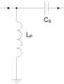
传统的Γ形匹配网络分为两种方案,一种如图3所示,即串联电路单元选用为电感而并联电路单元选用为电容。此时由于串联电路单元选用的为电感元件,那么同时为了使电感的调节作用更连续,也考虑到导航射频信号的接收与处理需要进行隔直的原因,在Γ形结构匹配网络的串联电路单元中,采用电感串联电容来替换原来网络中串联的电感。串联电容不仅起到隔直的作用,还可以弥补电感的不连续性,等效于对电感的微调。另一种传统的方案如图4所示,即串联电路单元选用为电容而并联电路单元选用为电感。此方案中,作为并联电路单元的电感一般会因电感的值不连续而影响调节作用的连续程度。但无论是方案一还是方案二,在不同初始阻抗下,其适用性都有缺陷。两种方案的选择取决于初始阻抗的特性。The traditional Γ-shaped matching network is divided into two schemes, one is shown in Figure 3, that is, the series circuit unit is selected as an inductor and the parallel circuit unit is selected as a capacitor. At this time, since the series circuit unit is selected as an inductance element, at the same time, in order to make the adjustment of the inductance more continuous, and also considering the reason that the reception and processing of the navigation radio frequency signal needs to be blocked directly, the series circuit unit of the Γ-shaped structure matching network In , the inductance in series with the capacitor is used to replace the inductance in series in the original network. The series capacitor not only plays the role of blocking DC, but also can make up for the discontinuity of the inductance, which is equivalent to fine-tuning the inductance. Another traditional scheme is shown in FIG. 4 , that is, the series circuit unit is selected as a capacitor and the parallel circuit unit is selected as an inductor. In this solution, the inductance as a parallel circuit unit generally affects the continuity of the adjustment effect due to the discontinuous value of the inductance. However, no matter it is the first or second scheme, its applicability is flawed under different initial impedances. The choice of the two schemes depends on the characteristics of the initial impedance.
频率越高时,阻抗匹配的效果越明显。射频接收机的输入端需要良好的匹配才能稳定的工作。由于IC流片时的工艺偏差以及封装后键合线的寄生参数不一致,导致最终封装的芯片输入阻抗不一致。如果在IC设计时将固定的校准元件集成到芯片内部,单纯依靠根据理论计算而得出的匹配网络的各器件的值往往不能合理的匹配到传输线的50欧姆特征阻抗,因此在IC设计时是实现不了理想的阻抗匹配的。所以传统的射频接收机的输入匹配网络只能由外电路的电感、电容来实现匹配,包括分布电容、引线电感等参数。The higher the frequency, the more obvious the effect of impedance matching. The input of the RF receiver needs to be well matched to work stably. Due to the process deviation during IC tape-out and the inconsistency of the parasitic parameters of the bonding wire after packaging, the input impedance of the final packaged chip is inconsistent. If the fixed calibration components are integrated into the chip during IC design, the values of the components of the matching network obtained purely based on theoretical calculations often cannot be reasonably matched to the 50 ohm characteristic impedance of the transmission line. Ideal impedance matching cannot be achieved. Therefore, the input matching network of the traditional RF receiver can only be matched by the inductance and capacitance of the external circuit, including parameters such as distributed capacitance and lead inductance.
传统的匹配网络只是一个固定的组合,如图3或图4所示的Γ形的拓扑结构。在外部电路设计完成之后网络中各部分器件的值是固定的,在需要作调整时虽然可以通过手动替换元器件来修改网络的匹配组合,但是元件替换起来不方便,且容易人为地引入非理想的寄生等因素,导致更大的工作量。因此传统的通过外电路进行匹配的方式比较刻板,很受约束,增加了研发中的诸多不便,加大了研发周期。The traditional matching network is just a fixed combination, such as the Γ-shaped topology shown in Figure 3 or Figure 4 . After the external circuit design is completed, the values of each component in the network are fixed. Although the matching combination of the network can be modified by manually replacing the components when adjustments are required, it is inconvenient to replace the components, and it is easy to artificially introduce non-ideal components. Factors such as parasitics lead to a greater workload. Therefore, the traditional way of matching through external circuits is relatively rigid and constrained, which increases a lot of inconvenience in research and development and increases the development cycle.
无线通信产业的迅猛发展,推动了射频前端电路设计向着高性能、低成本、高集成度的方向演变。因而,作为一种性能优、综合成本低、可集成、操作方便快捷的阻抗匹配方式,可通过配置指令实现匹配调谐的可配置匹配网络具有绝对的优势。The rapid development of the wireless communication industry has promoted the evolution of the RF front-end circuit design toward high performance, low cost, and high integration. Therefore, as an impedance matching method with excellent performance, low overall cost, integration, and convenient and quick operation, the configurable matching network that can realize matching and tuning through configuration commands has absolute advantages.
发明内容Contents of the invention
本发明对传统的匹配网络做了优化改进,融合两种传统匹配方案的优点,解决了两种传统匹配方案的缺点,提供一种可配置的匹配网络。The invention optimizes and improves the traditional matching network, integrates the advantages of two traditional matching schemes, solves the shortcomings of the two traditional matching schemes, and provides a configurable matching network.
一种用于卫星导航射频前端的可配置的匹配网络,包括并联电路单元和串联电路单元,其特征在于:所述的并联电路单元包括并联连接的并联开关电容阵列(11)和并联开关电感阵列(12);所述的串联电路单元包括依次串联连接的串联开关电感阵列(13)和串联开关电容阵列(14);天线送入的射频信号首先进入并联开关电容阵列(11)和并联开关电感阵列(12),经过并联开关电容阵列(11)和并联开关电感阵列(12)处理后送入串联连接的串联开关电感阵列(13),串联开关电感阵列(13)的输出信号直接送入串联开关电容阵列(14),之后再输出至后级电路;A configurable matching network for a satellite navigation radio frequency front end, comprising a parallel circuit unit and a series circuit unit, characterized in that: the parallel circuit unit includes a parallel switched capacitor array (11) and a parallel switched inductor array connected in parallel (12); the series circuit unit comprises a series switched inductor array (13) and a series switched capacitor array (14) connected in series; the radio frequency signal sent by the antenna first enters the parallel switched capacitor array (11) and the parallel switched inductor The array (12), after being processed by the parallel switched capacitor array (11) and the parallel switched inductor array (12), is sent to the series connected series switched inductor array (13), and the output signal of the series switched switched inductor array (13) is directly sent to the series A switched capacitor array (14), and then output to the subsequent stage circuit;
串联开关电感阵列(13)与串联开关电容阵列(14),用于对串联电路单元后面连接后级电路的阻抗进行第一步变换;The series switched inductor array (13) and the series switched capacitor array (14) are used to perform the first step of transforming the impedance of the subsequent stage circuit connected behind the series circuit unit;
并联开关电容阵列(11)与并联开关电感阵列(12),用于对第一步变换后的后级电路的阻抗进行进一步变换,将后级电路的初始阻抗变换到史密斯圆图的中心,完成阻抗匹配。The parallel switched capacitor array (11) and the parallel switched inductance array (12) are used to further transform the impedance of the post-stage circuit after the first step transformation, and transform the initial impedance of the post-stage circuit to the center of the Smith chart to complete Impedance matching.
其中,所述的并联开关电容阵列(11)由N个子电路并联组成,每个子电路由MOS管和电容构成;其中,N为大于1的自然数;电容的一端接输入信号连接线,电容的另一端接MOS管的漏极,MOS管的栅极接控制信号,MOS管的源极接地。Wherein, the parallel switched capacitor array (11) is composed of N sub-circuits connected in parallel, and each sub-circuit is composed of a MOS transistor and a capacitor; wherein, N is a natural number greater than 1; one end of the capacitor is connected to the input signal connection line, and the other end of the capacitor One end is connected to the drain of the MOS transistor, the gate of the MOS transistor is connected to the control signal, and the source of the MOS transistor is grounded.
其中,所述的串联开关电容阵列(14)由M个子电路并联组成,每个子电路由MOS管和电容构成;其中,M为大于1的自然数;其中一个子电路中的MOS管的源极接串联开关电感阵列(13)的输出,MOS管的栅极接控制信号,其MOS管的漏极接后级电路;其余子电路中的MOS管的源极接串联开关电感阵列(13)的输出,MOS管的栅极接控制信号,MOS管的漏极接电容的一端,电容的另一端接后级电路。Wherein, the series switched capacitor array (14) is composed of M sub-circuits connected in parallel, and each sub-circuit is composed of a MOS tube and a capacitor; wherein, M is a natural number greater than 1; the source of the MOS tube in one of the sub-circuits is connected The output of the series switch inductance array (13), the gate of the MOS tube is connected to the control signal, and the drain of the MOS tube is connected to the subsequent stage circuit; the sources of the MOS tubes in the remaining sub-circuits are connected to the output of the series switch inductance array (13) The gate of the MOS tube is connected to the control signal, the drain of the MOS tube is connected to one end of the capacitor, and the other end of the capacitor is connected to the subsequent circuit.
其中,所述的串联开关电感阵列(13)由N个子电路串联组成,每个子电路由MOS管和电感构成;其中,N为大于1的自然数;电感的一端接前级电路的输出和MOS管的源极,电感的另一端接MOS管的漏极,MOS管的栅极接控制信号。Wherein, the series switch inductor array (13) is composed of N sub-circuits in series, and each sub-circuit is composed of a MOS tube and an inductor; wherein, N is a natural number greater than 1; one end of the inductor is connected to the output of the previous stage circuit and the MOS tube The source of the inductor, the other end of the inductor is connected to the drain of the MOS transistor, and the gate of the MOS transistor is connected to the control signal.
其中,所述的并联开关电感阵列(12)由N个子电路串联组成,每个子电路由MOS管和电感构成;其中,N为大于1的自然数;其中一个子电路中的MOS管的漏极接天线的输入信号线,MOS管的栅极接控制信号,其MOS管的源极接并联开关电感阵列(12)中下级MOS管的漏极;其余子电路中的MOS管的漏极接并联开关电感阵列(12)中上级MOS管的源极,MOS管的栅极接控制信号,MOS管的漏极接电感的一端,MOS管的源极接电感的另一端;在并联开关电感阵列(12)中,最后一级MOS管的源极接地。Wherein, the parallel switch inductor array (12) is composed of N sub-circuits in series, and each sub-circuit is composed of a MOS tube and an inductor; wherein, N is a natural number greater than 1; the drain of the MOS tube in one of the sub-circuits is connected to The input signal line of the antenna, the gate of the MOS tube is connected to the control signal, and the source of the MOS tube is connected to the drain of the lower-level MOS tube in the parallel switch inductance array (12); the drains of the MOS tubes in the remaining sub-circuits are connected to the parallel switch In the inductance array (12), the source of the superior MOS tube, the gate of the MOS tube is connected to the control signal, the drain of the MOS tube is connected to one end of the inductor, and the source of the MOS tube is connected to the other end of the inductor; in the parallel switch inductor array (12 ), the source of the last stage MOS tube is grounded.
并联开关电容阵列11由N个子电路并联组成,每个子电路由MOS管和电容构成;其中,N为大于1的自然数;电容的一端接输入信号连接线,电容的另一端接MOS管的漏极,MOS管的栅极接控制信号,MOS管的源极接地。The parallel switched
控制信号Si控制MOS管的接通或关断,实现相应电容接入阵列电路。并联开关电容阵列11的控制信号S为一个N位的二进制数字信号,二进制信号的每一位Si控制一个子电路。当最低位子电路中的特定电容的容抗选定为C时,每个子电路中的特定电容的容抗就已确定,为2i*C。N个子电路并联构成整个并联开关电容阵列11,使得该并联开关电容阵列11接入整个网路的等效电容的容抗可以在0~(2N-1)*C的范围内变化,分辨率精度为C。The control signal Si controls the switching on or off of the MOS tube, so as to realize the connection of the corresponding capacitors into the array circuit. The control signal S of the parallel switched
在串联开关电容阵列14中,前N-1个子电路与所述的一组并联开关电容阵列11的子电路具有相同的结构,但,MOS管的源极接前级电路的输出。数字信号最高位S″N-1所控制的子电路仅由一个MOS管M″N-1构成。当子电路的MOS管M″N-1关断时,低N-1位的控制方式和实现功能与所述的并联开关电容阵列11的低N-1位相同。当MOS管M″N-1导通时,整个串联开关电容阵列14被导通的MOS管短路,此时无论阵列中低N-1位状态如何,该阵列不参与匹配调谐。N个子电路并联组成阵列,串联接入匹配网络电路。In the series switched
串联开关电感阵列13由N个子电路串联组成,每个子电路由MOS管和电感构成;其中,N为大于1的自然数;电感的一端接输入信号连接线和MOS管的源极,电感的另一端接MOS管的漏极,MOS管的栅极接控制信号。The series
控制信号S'i控制MOS管的接通或关断,实现相应的电感接入阵列电路。串联开关电感阵列13的控制信号S'为一个N位的二进制数字信号,二进制信号的每一位S'i控制一个子电路。当最低位子电路中的特定电感的感抗选定为L时,每个子电路中的特定电感的感抗就已确定,为2i*L。N个子电路串联构成整个串联开关电感阵列13,使得该电感阵列接入整个网路的等效电感的大小可以在0~(2N-1)*L的范围内变化,分辨率精度为L。The control signalS'i controls the switching on or off of the MOS tube, and realizes that the corresponding inductance is connected to the array circuit. The control signal S' of the series
在并联开关电感阵列12中,前N-1个子电路与所述的一组串联开关电感阵列13的子电路具有相同的结构;数字信号最高位S″'N-1所控制的子电路仅由一个MOS管M″′N-1构成。当子电路的MOS管M″′N-1导通时,低N-1位的控制方式和实现功能与所述的串联开关电感阵列13的低N-1位相同。当MOS管M″′N-1关断时,整个并联开关电感阵列12与匹配网络断开连接,此时无论阵列中低N-1位状态如何,该阵列不参与匹配调谐。N个子电路串联组成阵列,并联接入匹配网络电路。In the parallel
本发明与现有技术相比的有益效果为:The beneficial effects of the present invention compared with prior art are:
本发明用于集成在IC内部,可以方便地通过控制指令对射频前端系统实现输入特征阻抗匹配,操作简单快捷。同时简化了射频前端芯片的外电路,减少了外电路的器件数量,为研发过程节约时间及成本,适用于集成在各种射频前端芯片内部,应用广泛。The invention is used for integration in the IC, and can conveniently realize input characteristic impedance matching for the radio frequency front-end system through control instructions, and the operation is simple and fast. At the same time, the external circuit of the RF front-end chip is simplified, the number of devices in the external circuit is reduced, and time and cost are saved for the research and development process. It is suitable for integration in various RF front-end chips and has a wide range of applications.
附图说明Description of drawings
图1用于卫星导航射频前端的可配置的匹配网络示意图Figure 1 Schematic diagram of a configurable matching network for satellite navigation RF front-end
图2用于卫星导航射频前端的可配置的匹配网络具体实施方式示意图Figure 2 is a schematic diagram of a specific implementation of a configurable matching network for a satellite navigation radio frequency front end
图3传统电路中应用的匹配网络电路方案一示意图;Fig. 3 is a schematic diagram of a matching network circuit solution applied in a traditional circuit;
图4传统电路中应用的匹配网络电路方案二示意图;The second schematic diagram of the matching network circuit scheme applied in the traditional circuit of Fig. 4;
图5二进制加权开关电容阵列的子电路示意图;The subcircuit schematic diagram of Fig. 5 binary weighted switched capacitor array;
图6二进制加权开关电感阵列的子电路示意图;The subcircuit schematic diagram of Fig. 6 binary weighted switching inductance array;
图7匹配网络实现阻抗匹配的牵引路径示意图。Fig. 7 is a schematic diagram of a traction path for impedance matching by a matching network.
具体实施方式Detailed ways
为了使本发明的目的、技术方案和应用优越性更加清楚明白,下面结合附图对本发明的具体实施方式作进一步详细说明。In order to make the purpose, technical solution and application superiority of the present invention clearer, the specific implementation manners of the present invention will be further described in detail below in conjunction with the accompanying drawings.
图2基本组成原理框图所示的是采用本发明的可配置的匹配网络。连接于射频信号接收端之后,LNA等射频前端处理单元之前。包括一组并联开关电容阵列11与一组并联开关电感阵列12的并联电路作为并联电路单元连接在射频信号接收端与地之间;一组串联开关电感阵列13和串联开关电容阵列14的串联电路作为串联电路单元,串联在射频信号接收端与LNA等射频前端处理模块之间。Figure 2 shows the basic composition block diagram of the configurable matching network of the present invention. Connected after the RF signal receiving end, before the RF front-end processing unit such as LNA. A parallel circuit comprising a group of parallel switched
并联开关电容阵列11由N(N为大于1的自然数)组相同子单元并联组成,如图5所示,每个子单元由MOS管和电容串联组成,N(N为大于1的自然数)组子电路中电容容抗值的选取满足二进制加权关系,精度的选取取决于射频前端芯片其他单元的参数。The parallel switched
并联开关电感阵列12由N(N为大于1的自然数)组子单元串联组成,前N-1个子单元有相同的结构,如图6所示,每个子单元由MOS管和电感并联组成,第N组子单元仅由一个MOS管构成。N组子电路中电感感抗值的选取满足二进制加权关系,精度的选取取决于射频前端芯片其他单元的参数。The parallel
串联开关电感阵列13由N(N为大于1的自然数)组相同子单元串联组成,如图6所示,每个子单元由MOS管和电感并联组成,N组子电路中电感感抗值的选取满足二进制加权关系,精度的选取取决于射频前端芯片其他单元的参数。The series
串联开关电容阵列14由N(N为大于1的自然数)组子单元并联组成,前N-1个子单元有相同的结构,如图5所示,每个子单元由MOS管和电容串联组成,第N组子单元仅由一个MOS管构成。N组子电路中电容容抗值的选取满足二进制加权关系,精度的选取取决于射频前端芯片其他单元的参数。The series switched
在窄带阻抗匹配中,当阻抗匹配网络中并联插入一个电容时,插入电容的电纳ΔB=ΔBC为正,其幅度随着工作频率的增加而增加;插入一个并联电容CP,使得阻抗P沿史密斯圆图中的等电导圆顺时针移动,移动弧长由电容值决定。当阻抗匹配网络中并联插入一个电感时,插入电感的电纳ΔB=ΔBL为负,其幅度随着工作频率的增加而减少;插入一个并联电感LP,使得阻抗P沿着史密斯圆图中等电导圆逆时针移动,移动弧长由电感值决定。In narrow-band impedance matching, when a capacitor is inserted in parallel in the impedance matching network, the susceptance ΔB=ΔBC of the inserted capacitor is positive, and its amplitude increases with the increase of the operating frequency; inserting a parallel capacitor CP makes the impedance P Moving clockwise along the equal conductance circle in the Smith chart, the moving arc length is determined by the capacitance value. When an inductance is inserted in parallel in the impedance matching network, the susceptance ΔB=ΔBL of the inserted inductance is negative, and its amplitude decreases with the increase of the operating frequency; inserting a parallel inductance LP makes the impedance P along the Smith chart. The conductance circle moves counterclockwise, and the moving arc length is determined by the inductance value.
当阻抗匹配网络中串联插入一个电感时,插入的感抗ΔX=ΔXL为正,并且其幅度随着工作频率的增加而增加;插入串联电感LS使得阻抗P沿史密斯圆图的等电阻圆顺时针移动,移动的弧长由电感值决定。当阻抗匹配网络串联插入一个电容时,插入容抗ΔX=ΔXC为负,其幅度随工作频率的增加而减少;插入一个串联电容CS使得阻抗P沿史密斯圆图的等电阻圆逆时针移动,移动弧长由电容值决定。When an inductance is inserted in series in the impedance matching network, the inserted inductance ΔX=ΔXL is positive, and its amplitude increases with the increase of the operating frequency; inserting the series inductance LS makes the impedance P follow the equal resistance circle of the Smith chart Moving clockwise, the moving arc length is determined by the inductance value. When the impedance matching network inserts a capacitor in series, the inserted capacitance ΔX=ΔXC is negative, and its amplitude decreases with the increase of the operating frequency; inserting a series capacitor CS makes the impedance P move counterclockwise along the equal resistance circle of the Smith chart , the moving arc length is determined by the capacitance value.
在如图3所示的阻抗匹配网络中,串联电感LS增大时,使得初始阻抗P沿着史密斯圆图中的等电阻圆顺时针移动,移动弧长由电感值增大的多少决定。当串联电感LS减小时,使得初始阻抗P沿史密斯圆图中的等电阻圆逆时针移动,移动弧长由电感值减小的多少决定。在传统的匹配网络中,只能通过更换电感元件进行增大或减小的操作,在不断的调试匹配中,不仅工作量大、繁琐而且容易引入无法计算的寄生参数。而在所述的可配置的匹配网络中,只用简单的通过数字信号控制串联开关电感阵列13,改变某一位或多位MOS管的导通或关断状态,就可实现整个阵列的等效感抗的改变,可等价地看作串联电感LS的增大或减小,完成初始阻抗P在史密斯圆图中沿等电阻圆的顺时针或逆时针的移动。初步完成对初始阻抗P的牵引以实现阻抗匹配。In the impedance matching network shown in Figure 3, when the series inductance LS increases, the initial impedance P moves clockwise along the equal resistance circle in the Smith chart, and the moving arc length is determined by the increase of the inductance value. When the series inductance LS decreases, the initial impedance P moves counterclockwise along the equal-resistance circle in the Smith chart, and the moving arc length is determined by how much the inductance value decreases. In the traditional matching network, the operation of increasing or decreasing can only be performed by replacing the inductance element. In the continuous debugging and matching, not only the workload is heavy and cumbersome, but also it is easy to introduce parasitic parameters that cannot be calculated. In the above-mentioned configurable matching network, only by simply controlling the series
在如图3所示的阻抗匹配网络中,并联电容CP增大时,使得初始阻抗P沿史密斯圆图中的等电导圆顺时针移动,移动弧长由电容值的增大的多少决定。当并联电容CP减小时,使得初始阻抗P沿史密斯圆图中的等电导圆逆时针移动,移动弧长由电容值减小的多少决定。与传统的匹配网络相比,所述的可配置的匹配网络中,同样只用简单的通过数字信号控制并联开关电容阵列11,来完成初始阻抗P在史密斯圆图中沿等电导圆的顺时针或逆时针的移动。从而进一步将初始阻抗P牵引到史密斯圆图的中心。In the impedance matching network shown in Figure 3, when the parallel capacitance CP increases, the initial impedance P moves clockwise along the equal conductance circle in the Smith chart, and the moving arc length is determined by the increase of the capacitance value. When the parallel capacitor CP decreases, the initial impedance P moves counterclockwise along the equal conductance circle in the Smith chart, and the moving arc length is determined by how much the capacitance value decreases. Compared with the traditional matching network, the configurable matching network also only uses a simple digital signal to control the parallel switched
在所述的用于卫星导航射频前端的可配置匹配网络中,为了弥补传统方案一在电路匹配上灵活性差、调试复杂等方面的缺陷,对并联电路单元级并联入一组并联开关电感阵列12。当阻抗匹配网络中并联电感LP增大时,使得初始阻抗P沿着史密斯圆图中的等电导圆逆时针移动;并联电感LP减小时,使得初始阻抗P沿着史密斯圆图中的等电导圆顺时针移动,移动弧长由电感值增大或减小的多少决定。在所述的用于卫星导航射频前端的可配置匹配网络中,对并联开关电感阵列12的控制方式与对串联开关电感阵列13的控制方式相同。In the configurable matching network for satellite navigation radio frequency front-end described above, in order to make up for the shortcomings of the traditional scheme 1 in terms of poor flexibility in circuit matching and complicated debugging, a group of parallel
在所述的用于卫星导航射频前端的可配置匹配网络中,为了使串联开关电感阵列13的调节作用更连续,同样在Γ形网络后串联了串联开关电容阵列14以弥补串联开关电感阵列13变化时的不连续性,同时可对后级的放大等处理单元作隔直保护。串联电容CS增大时,使得初始阻抗P沿史密斯圆图中的等电阻圆逆时针移动;当串联电容CS减小时,使得初始阻抗P沿史密斯圆图中的等电阻圆顺时针移动,移动弧长由电容值增大或减小的多少决定。串联电容对初始阻抗P的牵引作用相比串联电感的作用较弱,因此用电容对电感的牵引作用作微调。在所述的用于卫星导航射频前端的可配置匹配网络中,对串联开关电容阵列14的控制方式与对并联开关电容阵列11的控制方式相同。In the configurable matching network used for satellite navigation radio frequency front-end, in order to make the adjustment function of the series
图2所示的结构是采用此种用于卫星导航射频前端的可配置的匹配网络对射频接收信号进行传输时,对射频前端芯片进行阻抗匹配的应用结构示意图。当天线接收到射频信号后,传输至射频前端芯片输入端口。为了保证射频模块完成在无相移情况下的最大功率传输,在射频前端芯片的输入端口集成了此种用于卫星导航射频前端的可配置的匹配网络,射频信号传输经过该匹配网络后进入低噪放及其它的射频信号放大、下变频、滤波等处理单元。如前面所述,当输入端口阻抗匹配不合理时,会产生反射,因此需要由上位机发送数字控制信号,通过SPI口配置射频前端芯片内部相应的寄存器,对电容阵列的等效容抗以及电感阵列的等效感抗进行调控,先通过调控串联电路单元中的串联开关电感阵列13与串联开关电容阵列14对后级电路的初始阻抗进行第一步牵引,然后对并联电路单元中的并联开关电容阵列11与并联开关电感阵列12进行配置,对第一步中的阻抗进行进一步的牵引,并最终将初始阻抗牵引到史密斯圆图的中心,从而将整个射频前端的输入特征阻抗调整匹配到50欧姆,实现匹配的调控。例如,当初始阻抗P的归一化阻抗位于史密斯圆图的某一区域,如图7所示位置时,这种方案可以将初始阻抗P牵引到史密斯圆图的中心O。沿P-A-O路径的牵引,首先第一步,先通过将串联开关电感阵列13的等效电感调小合适的值,或将串联开关电容阵列13的等效电容调大合适的值,将初始阻抗P沿等电阻圆牵引至A点;第二步,再通过将串联开关电容阵列14的等效电容值调大适当值,或将并联开关电感阵列12的等效电感值调小适当值,即可将初始阻抗沿等电导圆由A点牵引至史密斯圆图的中心O。The structure shown in FIG. 2 is a schematic diagram of an application structure for performing impedance matching on a radio frequency front-end chip when such a configurable matching network for a satellite navigation radio frequency front-end is used to transmit a radio frequency receiving signal. When the antenna receives the radio frequency signal, it is transmitted to the input port of the radio frequency front-end chip. In order to ensure that the RF module completes the maximum power transmission without phase shift, the input port of the RF front-end chip integrates such a configurable matching network for the satellite navigation RF front-end. Noise amplifier and other RF signal amplification, frequency down conversion, filtering and other processing units. As mentioned earlier, when the impedance matching of the input port is unreasonable, reflections will occur, so the host computer needs to send digital control signals, and configure the corresponding registers inside the RF front-end chip through the SPI port, and the equivalent capacitive reactance and inductance of the capacitor array The equivalent inductance of the array is regulated. Firstly, the initial impedance of the subsequent stage circuit is drawn by regulating the series
以上所述,仅为本发明的一种具体的实施方式。这种实现方式为Γ型网络的一种,另外还有T型、Π型等。本发明的保护范围并不局限于此,任何熟悉本技术领域的技术人员在本发明揭露的技术范围内,可轻易想到的变化或替换,都应涵盖在本发明的保护范围之内。The above is only a specific implementation manner of the present invention. This implementation is a kind of Γ-type network, and there are T-type, Π-type and so on. The protection scope of the present invention is not limited thereto, and any changes or substitutions that can be easily conceived by those skilled in the art within the technical scope disclosed in the present invention shall fall within the protection scope of the present invention.
Claims (5)
Translated fromChinesePriority Applications (1)
| Application Number | Priority Date | Filing Date | Title |
|---|---|---|---|
| CN201310413367.1ACN103454654B (en) | 2013-09-11 | 2013-09-11 | Configurable matching network used at satellite navigation radio frequency front end |
Applications Claiming Priority (1)
| Application Number | Priority Date | Filing Date | Title |
|---|---|---|---|
| CN201310413367.1ACN103454654B (en) | 2013-09-11 | 2013-09-11 | Configurable matching network used at satellite navigation radio frequency front end |
Publications (2)
| Publication Number | Publication Date |
|---|---|
| CN103454654Atrue CN103454654A (en) | 2013-12-18 |
| CN103454654B CN103454654B (en) | 2015-03-18 |
Family
ID=49737226
Family Applications (1)
| Application Number | Title | Priority Date | Filing Date |
|---|---|---|---|
| CN201310413367.1AActiveCN103454654B (en) | 2013-09-11 | 2013-09-11 | Configurable matching network used at satellite navigation radio frequency front end |
Country Status (1)
| Country | Link |
|---|---|
| CN (1) | CN103454654B (en) |
Cited By (12)
| Publication number | Priority date | Publication date | Assignee | Title |
|---|---|---|---|---|
| CN104582146A (en)* | 2014-12-17 | 2015-04-29 | 深圳市众明半导体照明有限公司 | Led drive circuit |
| CN105187086A (en)* | 2014-06-11 | 2015-12-23 | Lg伊诺特有限公司 | Rf module |
| CN105917581A (en)* | 2014-01-17 | 2016-08-31 | 高通股份有限公司 | Switchable antenna array |
| CN106571788A (en)* | 2016-11-03 | 2017-04-19 | 青岛海信移动通信技术股份有限公司 | Multiband matching circuit, radio frequency circuit, antenna system and mobile terminal |
| CN107408845A (en)* | 2015-03-20 | 2017-11-28 | 曼珀斯有限公司 | Wireless power receiver |
| CN108832907A (en)* | 2018-05-25 | 2018-11-16 | 广州中海达卫星导航技术股份有限公司 | Data radio station wideband impedance match network and its design method |
| CN109120301A (en)* | 2018-07-13 | 2019-01-01 | 安凯(广州)微电子技术有限公司 | A kind of tuner and method of transmitting and reception community network |
| CN111030726A (en)* | 2019-12-13 | 2020-04-17 | 展讯通信(上海)有限公司 | Radio frequency front end control circuit and control method thereof, radio frequency front end control chip, system, storage medium and terminal |
| CN111786570A (en)* | 2020-06-17 | 2020-10-16 | 西安易恩电气科技有限公司 | High-power automatic programmable inductance device |
| CN113098425A (en)* | 2021-03-30 | 2021-07-09 | 徐显坤 | Impedance matching network, adaptive impedance matching device and method thereof |
| WO2021227280A1 (en)* | 2020-05-14 | 2021-11-18 | 锐石创芯(深圳)科技有限公司 | Radio-frequency front-end module and wireless apparatus |
| CN119602736A (en)* | 2024-11-07 | 2025-03-11 | 中国科学院声学研究所 | An adaptive impedance matching device for underwater low-frequency hydroacoustic transducer |
Citations (6)
| Publication number | Priority date | Publication date | Assignee | Title |
|---|---|---|---|---|
| US20040253939A1 (en)* | 2003-06-12 | 2004-12-16 | Castaneda Jesus A. | Integrated circuit radio front-end architecture and applications thereof |
| CN101150296A (en)* | 2007-11-07 | 2008-03-26 | 北京航空航天大学 | A low noise amplifier for wireless communication and navigation receiver and its realization method |
| CN101183878A (en)* | 2007-12-20 | 2008-05-21 | 复旦大学 | A low-power wireless receiver radio frequency front-end circuit |
| CN102075208A (en)* | 2010-12-31 | 2011-05-25 | 东南大学 | Radio frequency front-end with low power consumption |
| CN102096079A (en)* | 2009-12-12 | 2011-06-15 | 杭州中科微电子有限公司 | Method for constructing radio frequency front end of multi-mode multi-band satellite navigation receiver and module thereof |
| CN102340294A (en)* | 2010-07-21 | 2012-02-01 | 中国科学院微电子研究所 | Four-order active LC radio frequency band-pass filter |
- 2013
- 2013-09-11CNCN201310413367.1Apatent/CN103454654B/enactiveActive
Patent Citations (6)
| Publication number | Priority date | Publication date | Assignee | Title |
|---|---|---|---|---|
| US20040253939A1 (en)* | 2003-06-12 | 2004-12-16 | Castaneda Jesus A. | Integrated circuit radio front-end architecture and applications thereof |
| CN101150296A (en)* | 2007-11-07 | 2008-03-26 | 北京航空航天大学 | A low noise amplifier for wireless communication and navigation receiver and its realization method |
| CN101183878A (en)* | 2007-12-20 | 2008-05-21 | 复旦大学 | A low-power wireless receiver radio frequency front-end circuit |
| CN102096079A (en)* | 2009-12-12 | 2011-06-15 | 杭州中科微电子有限公司 | Method for constructing radio frequency front end of multi-mode multi-band satellite navigation receiver and module thereof |
| CN102340294A (en)* | 2010-07-21 | 2012-02-01 | 中国科学院微电子研究所 | Four-order active LC radio frequency band-pass filter |
| CN102075208A (en)* | 2010-12-31 | 2011-05-25 | 东南大学 | Radio frequency front-end with low power consumption |
Cited By (14)
| Publication number | Priority date | Publication date | Assignee | Title |
|---|---|---|---|---|
| CN105917581B (en)* | 2014-01-17 | 2019-09-17 | 高通股份有限公司 | Switchable Antenna Array |
| CN105917581A (en)* | 2014-01-17 | 2016-08-31 | 高通股份有限公司 | Switchable antenna array |
| CN105187086A (en)* | 2014-06-11 | 2015-12-23 | Lg伊诺特有限公司 | Rf module |
| CN104582146A (en)* | 2014-12-17 | 2015-04-29 | 深圳市众明半导体照明有限公司 | Led drive circuit |
| CN107408845A (en)* | 2015-03-20 | 2017-11-28 | 曼珀斯有限公司 | Wireless power receiver |
| CN106571788A (en)* | 2016-11-03 | 2017-04-19 | 青岛海信移动通信技术股份有限公司 | Multiband matching circuit, radio frequency circuit, antenna system and mobile terminal |
| CN108832907A (en)* | 2018-05-25 | 2018-11-16 | 广州中海达卫星导航技术股份有限公司 | Data radio station wideband impedance match network and its design method |
| CN109120301A (en)* | 2018-07-13 | 2019-01-01 | 安凯(广州)微电子技术有限公司 | A kind of tuner and method of transmitting and reception community network |
| CN111030726A (en)* | 2019-12-13 | 2020-04-17 | 展讯通信(上海)有限公司 | Radio frequency front end control circuit and control method thereof, radio frequency front end control chip, system, storage medium and terminal |
| WO2021227280A1 (en)* | 2020-05-14 | 2021-11-18 | 锐石创芯(深圳)科技有限公司 | Radio-frequency front-end module and wireless apparatus |
| CN111786570A (en)* | 2020-06-17 | 2020-10-16 | 西安易恩电气科技有限公司 | High-power automatic programmable inductance device |
| CN113098425A (en)* | 2021-03-30 | 2021-07-09 | 徐显坤 | Impedance matching network, adaptive impedance matching device and method thereof |
| CN119602736A (en)* | 2024-11-07 | 2025-03-11 | 中国科学院声学研究所 | An adaptive impedance matching device for underwater low-frequency hydroacoustic transducer |
| CN119602736B (en)* | 2024-11-07 | 2025-09-02 | 中国科学院声学研究所 | An adaptive impedance matching device for underwater low-frequency underwater acoustic transducer |
Also Published As
| Publication number | Publication date |
|---|---|
| CN103454654B (en) | 2015-03-18 |
Similar Documents
| Publication | Publication Date | Title |
|---|---|---|
| CN103454654A (en) | Configurable matching network used at satellite navigation radio frequency front end | |
| CN113572440B (en) | Power amplifier output matching circuit, radio frequency front end module and wireless device | |
| CN103326684B (en) | Adjustable impedance matching network | |
| KR101699170B1 (en) | System and method for a low noise amplifier | |
| US10141971B1 (en) | Transceiver circuit having a single impedance matching network | |
| CN107005216B (en) | Attenuator | |
| US8886136B1 (en) | Two-pin TR switch with switched capacitor | |
| CN1965475A (en) | Variable matching circuit | |
| CN106712736B (en) | Adjustable passive network of broadband | |
| US20240088837A1 (en) | Low noise amplification circuit | |
| CN204013405U (en) | Tunable high-efficiency power amplifier supporting multiple frequency bands | |
| EP3189587A1 (en) | Dynamic power divider circuits and methods | |
| US9473101B2 (en) | Amplifier with integral notch filter | |
| US20170187338A1 (en) | Amplifier with coupled inductors | |
| CN103023431B (en) | A method of improving voltage controlled oscillator tuning range and phase noise performance | |
| US20240314002A1 (en) | Input impedance matching network and radio frequency front-end module | |
| CN103916084A (en) | Gain adjustable low noise amplifier circuit | |
| JP2013201757A (en) | Impedance adjustment by amplifier | |
| CN105099479A (en) | Radio-frequency front-end circuit of multi-mode intelligent terminal receiver | |
| CN111162814B (en) | Impedance adjusters, RF circuits and electronic equipment | |
| CN114124029B (en) | Second-order adjustable LC notch filter for polar zero tracking | |
| CN102577121B (en) | Fine grain tuning | |
| CN104579307B (en) | A kind of Q values lifting circuit of RF passive inductance | |
| CN203368415U (en) | Electric-tuning filter | |
| CN108365823B (en) | Voltage-controlled varactor circuit of big varactor ratio based on field effect transistor |
Legal Events
| Date | Code | Title | Description |
|---|---|---|---|
| C06 | Publication | ||
| PB01 | Publication | ||
| C10 | Entry into substantive examination | ||
| SE01 | Entry into force of request for substantive examination | ||
| C14 | Grant of patent or utility model | ||
| GR01 | Patent grant |