CN103441108A - Chip front-mounting BGA encapsulating structure - Google Patents
Chip front-mounting BGA encapsulating structureDownload PDFInfo
- Publication number
- CN103441108A CN103441108ACN2013103808097ACN201310380809ACN103441108ACN 103441108 ACN103441108 ACN 103441108ACN 2013103808097 ACN2013103808097 ACN 2013103808097ACN 201310380809 ACN201310380809 ACN 201310380809ACN 103441108 ACN103441108 ACN 103441108A
- Authority
- CN
- China
- Prior art keywords
- metal
- chip
- substrate
- bump
- bga
- Prior art date
- Legal status (The legal status is an assumption and is not a legal conclusion. Google has not performed a legal analysis and makes no representation as to the accuracy of the status listed.)
- Pending
Links
Images


Classifications
- H—ELECTRICITY
- H01—ELECTRIC ELEMENTS
- H01L—SEMICONDUCTOR DEVICES NOT COVERED BY CLASS H10
- H01L2224/00—Indexing scheme for arrangements for connecting or disconnecting semiconductor or solid-state bodies and methods related thereto as covered by H01L24/00
- H01L2224/01—Means for bonding being attached to, or being formed on, the surface to be connected, e.g. chip-to-package, die-attach, "first-level" interconnects; Manufacturing methods related thereto
- H01L2224/26—Layer connectors, e.g. plate connectors, solder or adhesive layers; Manufacturing methods related thereto
- H01L2224/31—Structure, shape, material or disposition of the layer connectors after the connecting process
- H01L2224/32—Structure, shape, material or disposition of the layer connectors after the connecting process of an individual layer connector
- H01L2224/321—Disposition
- H01L2224/32151—Disposition the layer connector connecting between a semiconductor or solid-state body and an item not being a semiconductor or solid-state body, e.g. chip-to-substrate, chip-to-passive
- H01L2224/32221—Disposition the layer connector connecting between a semiconductor or solid-state body and an item not being a semiconductor or solid-state body, e.g. chip-to-substrate, chip-to-passive the body and the item being stacked
- H01L2224/32225—Disposition the layer connector connecting between a semiconductor or solid-state body and an item not being a semiconductor or solid-state body, e.g. chip-to-substrate, chip-to-passive the body and the item being stacked the item being non-metallic, e.g. insulating substrate with or without metallisation
- H—ELECTRICITY
- H01—ELECTRIC ELEMENTS
- H01L—SEMICONDUCTOR DEVICES NOT COVERED BY CLASS H10
- H01L2224/00—Indexing scheme for arrangements for connecting or disconnecting semiconductor or solid-state bodies and methods related thereto as covered by H01L24/00
- H01L2224/01—Means for bonding being attached to, or being formed on, the surface to be connected, e.g. chip-to-package, die-attach, "first-level" interconnects; Manufacturing methods related thereto
- H01L2224/42—Wire connectors; Manufacturing methods related thereto
- H01L2224/47—Structure, shape, material or disposition of the wire connectors after the connecting process
- H01L2224/48—Structure, shape, material or disposition of the wire connectors after the connecting process of an individual wire connector
- H01L2224/481—Disposition
- H01L2224/48151—Connecting between a semiconductor or solid-state body and an item not being a semiconductor or solid-state body, e.g. chip-to-substrate, chip-to-passive
- H01L2224/48221—Connecting between a semiconductor or solid-state body and an item not being a semiconductor or solid-state body, e.g. chip-to-substrate, chip-to-passive the body and the item being stacked
- H01L2224/48225—Connecting between a semiconductor or solid-state body and an item not being a semiconductor or solid-state body, e.g. chip-to-substrate, chip-to-passive the body and the item being stacked the item being non-metallic, e.g. insulating substrate with or without metallisation
- H01L2224/48227—Connecting between a semiconductor or solid-state body and an item not being a semiconductor or solid-state body, e.g. chip-to-substrate, chip-to-passive the body and the item being stacked the item being non-metallic, e.g. insulating substrate with or without metallisation connecting the wire to a bond pad of the item
- H—ELECTRICITY
- H01—ELECTRIC ELEMENTS
- H01L—SEMICONDUCTOR DEVICES NOT COVERED BY CLASS H10
- H01L2224/00—Indexing scheme for arrangements for connecting or disconnecting semiconductor or solid-state bodies and methods related thereto as covered by H01L24/00
- H01L2224/73—Means for bonding being of different types provided for in two or more of groups H01L2224/10, H01L2224/18, H01L2224/26, H01L2224/34, H01L2224/42, H01L2224/50, H01L2224/63, H01L2224/71
- H01L2224/732—Location after the connecting process
- H01L2224/73251—Location after the connecting process on different surfaces
- H01L2224/73265—Layer and wire connectors
- H—ELECTRICITY
- H01—ELECTRIC ELEMENTS
- H01L—SEMICONDUCTOR DEVICES NOT COVERED BY CLASS H10
- H01L2224/00—Indexing scheme for arrangements for connecting or disconnecting semiconductor or solid-state bodies and methods related thereto as covered by H01L24/00
- H01L2224/91—Methods for connecting semiconductor or solid state bodies including different methods provided for in two or more of groups H01L2224/80 - H01L2224/90
- H01L2224/92—Specific sequence of method steps
- H01L2224/922—Connecting different surfaces of the semiconductor or solid-state body with connectors of different types
- H01L2224/9222—Sequential connecting processes
- H01L2224/92242—Sequential connecting processes the first connecting process involving a layer connector
- H01L2224/92247—Sequential connecting processes the first connecting process involving a layer connector the second connecting process involving a wire connector
- H—ELECTRICITY
- H01—ELECTRIC ELEMENTS
- H01L—SEMICONDUCTOR DEVICES NOT COVERED BY CLASS H10
- H01L2924/00—Indexing scheme for arrangements or methods for connecting or disconnecting semiconductor or solid-state bodies as covered by H01L24/00
- H01L2924/15—Details of package parts other than the semiconductor or other solid state devices to be connected
- H01L2924/151—Die mounting substrate
- H01L2924/153—Connection portion
- H01L2924/1531—Connection portion the connection portion being formed only on the surface of the substrate opposite to the die mounting surface
- H01L2924/15311—Connection portion the connection portion being formed only on the surface of the substrate opposite to the die mounting surface being a ball array, e.g. BGA
Landscapes
- Cooling Or The Like Of Semiconductors Or Solid State Devices (AREA)
Abstract
Translated fromChineseDescription
Translated fromChinese技术领域technical field
本发明涉及一种芯片正装BGA封装结构,属于半导体封装技术领域。The invention relates to a front-mounted chip BGA packaging structure, which belongs to the technical field of semiconductor packaging.
背景技术Background technique
现今,半导体封装产业为了满足各种高功耗芯片要求,其大多在BGA表面放置散热片(如图1所示),散热片虽然增加了封装TOP面的散热效果,但也因此增加了BGA产品的整体高度,很难应用于对BGA封装要求较薄的产品如手机、笔记本等手持设备,而AP等芯片由于考虑到多核运算等,其功率要求也越来越高,对散热的要求也越来越高,无散热片的形式难以胜任要求,但增加散热片又难以满足产品应用环境对厚度的要求。而且带散热片的BGA生产方法,通常是在BGA生产加工完后,再用胶料压合散热片,因此散热片并没有与基板或芯片表面的热源直接接触,其散热效果不好。Nowadays, in order to meet the requirements of various high power consumption chips in the semiconductor packaging industry, most of them place heat sinks on the surface of BGA (as shown in Figure 1). Although the heat sink increases the heat dissipation effect of the TOP surface of the package, it also increases the number of BGA products. The overall height is difficult to apply to products such as mobile phones, notebooks and other handheld devices that require thinner BGA packaging, and chips such as APs have higher power requirements and higher heat dissipation requirements due to multi-core computing. The higher the heat sink, the form without a heat sink is difficult to meet the requirements, but the addition of a heat sink is difficult to meet the thickness requirements of the product application environment. Moreover, the BGA production method with heat sink is usually after the BGA production and processing is completed, and then the heat sink is pressed with glue, so the heat sink does not directly contact the heat source on the substrate or chip surface, and its heat dissipation effect is not good.
发明内容Contents of the invention
本发明的目的在于克服上述不足,提供一种芯片正装BGA封装结构,它在不增加BGA封装厚度的情况下,通过封装工艺将金属凸块集成于BGA 塑封体上,凸块底面与基板表面或芯片表面相接触,凸块顶面通过电镀工艺使其与塑封料表面电镀金属层构成一个整体的散热装置,由于金属凸块直接与基板表面或芯片表面相连,热量可以直接传导至电镀金属层表面,并通过电镀金属层表面与空气的对流辐射作用,提高了整体散热效果。The object of the present invention is to overcome above-mentioned deficiency, provide a kind of chip to install BGA packaging structure, it is under the situation that does not increase BGA packaging thickness, integrates metal bump on the BGA plastic packaging body through packaging technology, and bump bottom surface and substrate surface or The surface of the chip is in contact, and the top surface of the bump is electroplated to form an integral heat sink with the electroplated metal layer on the surface of the plastic encapsulant. Since the metal bump is directly connected to the surface of the substrate or chip, the heat can be directly conducted to the surface of the electroplated metal layer. , and through the convective radiation effect between the surface of the electroplated metal layer and the air, the overall heat dissipation effect is improved.
本发明的目的是这样实现的:一种芯片正装BGA封装结构,它包括基板,所述基板正面通过导电或不导电粘结物质正装有芯片,所述芯片正面与基板正面之间通过金属线相连接,所述芯片正面设置有多个第二金属凸块,所述芯片周围的基板正面设置多个第一金属凸块,所述芯片、第一金属凸块和第二金属凸块外围的区域包封有塑封料,所述塑封料与第一金属凸块和第二金属凸块顶部齐平,所述塑封料正面电镀有金属层,所述金属层与第一金属凸块和第二金属凸块顶部相连接,所述基板背面设置有多个金属球。The object of the present invention is achieved in the following way: a front-mounted BGA packaging structure for chips, which includes a substrate, the front of the substrate is equipped with a chip through a conductive or non-conductive adhesive substance, and the front of the chip is connected to the front of the substrate by a metal wire. connection, the front of the chip is provided with a plurality of second metal bumps, the front of the substrate around the chip is provided with a plurality of first metal bumps, and the peripheral areas of the chip, the first metal bumps and the second metal bumps Encapsulated with molding compound, the molding compound is flush with the top of the first metal bump and the second metal bump, and the front side of the molding compound is electroplated with a metal layer, and the metal layer is in contact with the first metal bump and the second metal bump. The tops of the bumps are connected, and a plurality of metal balls are arranged on the back surface of the substrate.
更进一步的,所述塑封料侧面露出多个第一金属凸块。Furthermore, a plurality of first metal bumps are exposed on the side of the molding compound.
更进一步的,所述第一金属凸块和第二金属凸块的横截面形状为方形、圆形、六边形或八角形。Furthermore, the cross-sectional shape of the first metal bump and the second metal bump is square, circular, hexagonal or octagonal.
与现有技术相比,本发明具有以下有益效果:Compared with the prior art, the present invention has the following beneficial effects:
本发明一种芯片正装BGA封装结构,它在不增加BGA封装厚度的情况下,通过封装工艺将金属凸块集成于BGA 塑封体上,凸块底面与基板表面或芯片表面相接触,凸块顶面通过电镀工艺使其与塑封料表面电镀金属层构成一个整体散热装置,由于金属凸块直接与基板表面或芯片表面相连,热量可以直接传导至电镀金属层表面,并通过电镀金属层表面与空气的对流辐射作用,提高了整体散热效果;金属凸块可采用一些固定尺寸规格,方便批量生产,并且与基板、芯片表面的连接位置、接触面积可根据内部的结构、内部热点位置以及模流成型的需要进行灵活布置,有利于大批量生产,也克服了采用整块散热金属块因芯片大小不同、封装尺寸大小不同需要特制的现象。The present invention is a BGA packaging structure for front-loading chips, which integrates metal bumps on the BGA plastic package through a packaging process without increasing the thickness of the BGA package. The surface is electroplated to form an integral heat sink with the electroplated metal layer on the surface of the plastic packaging compound. Since the metal bump is directly connected to the surface of the substrate or chip, the heat can be directly conducted to the surface of the electroplated metal layer, and through the surface of the electroplated metal layer and the air. The convective radiation effect improves the overall heat dissipation effect; the metal bumps can adopt some fixed size specifications, which is convenient for mass production, and the connection position and contact area with the substrate and chip surface can be formed according to the internal structure, internal hot spot position and mold flow Flexible layout according to the needs of the environment is conducive to mass production, and it also overcomes the phenomenon that the whole heat dissipation metal block needs to be specially made due to different chip sizes and package sizes.
附图说明Description of drawings
图1为以往常见的散热型BGA的结构示意图。FIG. 1 is a schematic diagram of the structure of a common heat dissipation BGA in the past.
图2~图9为本发明一种芯片正装BGA封装结构制造方法的各工序示意图。2 to 9 are schematic diagrams of each process of a method for manufacturing a front-mounted chip BGA package structure according to the present invention.
图10为本发明一种芯片正装BGA封装结构的示意图。FIG. 10 is a schematic diagram of a front-mount BGA packaging structure of a chip according to the present invention.
图11为本发明一种芯片正装BGA封装结构另一实施例的示意图。FIG. 11 is a schematic diagram of another embodiment of a front-mount BGA packaging structure of a chip according to the present invention.
其中:in:
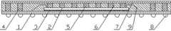
基板1Substrate 1
芯片2Chip 2
导电或不导电粘结物质3Conductive or non-conductive bonding substances3
第一金属凸块4first metal bump 4
第二金属凸块5Second metal bump 5
塑封料6
金属层7
金属球8
金属线9。metal wire9.
具体实施方式Detailed ways
参见图10,本发明一种芯片正装BGA封装结构,它包括基板1,所述基板1正面通过导电或不导电粘结物质3正装有芯片2,所述芯片2正面与基板1正面之间通过金属线9相连接,所述芯片2正面通过导热胶设置有多个第二金属凸块5,所述芯片2周围的基板1正面通过导热胶设置多个第一金属凸块4,所述第一金属凸块4与第二金属凸块5顶部齐平,所述芯片2、第一金属凸块4和第二金属凸块5外围的区域包封有塑封料6,所述塑封料6与第一金属凸块4和第二金属凸块5顶部齐平,所述塑封料6正面电镀有金属层7,所述金属层7与第一金属凸块4和第二金属凸块5顶部相连接,所述基板1背面设置有多个金属球8。Referring to FIG. 10 , a BGA packaging structure for front-mounting chips in the present invention includes a substrate 1, the front of the substrate 1 is equipped with a chip 2 through a conductive or non-conductive adhesive substance 3, and the front of the chip 2 and the front of the substrate 1 are passed through The metal wires 9 are connected, the front of the chip 2 is provided with a plurality of second metal bumps 5 through thermal conductive glue, and the front of the substrate 1 around the chip 2 is provided with a plurality of first metal bumps 4 through thermal conductive glue. A metal bump 4 is flush with the top of the second metal bump 5, and the peripheral area of the chip 2, the first metal bump 4 and the second metal bump 5 is encapsulated with a
所述第一金属凸块4和第二金属凸块5的横截面形状可以是方形、圆形、六边形、八角形等,金属凸块可以在SMT工序或装片工序进行安装。The cross-sectional shape of the first metal bump 4 and the second metal bump 5 can be square, circular, hexagonal, octagonal, etc., and the metal bumps can be installed in the SMT process or chip loading process.
其制造方法如下:Its manufacturing method is as follows:
步骤一、取一片基板Step 1. Take a piece of substrate
参见图2,取一片基板,基板上含有印刷电路,基板厚度的选择可依据产品特性进行选择;See Figure 2, take a piece of substrate, which contains printed circuits, and the thickness of the substrate can be selected according to product characteristics;
步骤二、装片Step 2, loading film
参见图3,在基板的正面通过导电或不导电粘结物质正装上芯片;Referring to Figure 3, the chip is being mounted on the front side of the substrate through a conductive or non-conductive adhesive substance;
步骤三、金属线键合Step 3. Wire bonding
参见图4,在芯片正面与基板正面之间进行键合金属线作业;Referring to Figure 4, the bonding metal wire operation is performed between the front side of the chip and the front side of the substrate;
步骤四、安装金属凸块Step 4. Install metal bumps
参见图5,在完成装片打线的芯片周围的基板正面通过导热胶安装上多个第一金属块,在芯片正面通过导热胶安装上多个第二金属块;Referring to Fig. 5, a plurality of first metal blocks are installed on the front of the substrate around the chip that has been mounted and wired through thermally conductive adhesive, and a plurality of second metal blocks are installed on the front of the chip through thermally conductive adhesive;
步骤五、塑封Step 5, plastic packaging
参加图6,在步骤四完成金属凸块安装的基板正面进行环氧树脂塑封保护,环氧树脂材料可以依据产品特性选择有填料或是没有填料的种类;Referring to Figure 6, the front side of the substrate where the metal bump is installed in step 4 is protected by epoxy resin molding. The epoxy resin material can be selected with or without filler according to product characteristics;
步骤六、研磨
参见图7,在步骤五完成环氧树脂塑封后进行表面研磨,使第一金属凸块和第二金属凸块顶部露出塑封料表面;Referring to Fig. 7, surface grinding is performed after the epoxy resin molding is completed in step 5, so that the tops of the first metal bump and the second metal bump are exposed to the surface of the molding compound;
步骤七、电镀金属层
参见图8,在步骤六完成研磨后的塑封料表面电镀上一层金属层;Referring to Fig. 8, a layer of metal layer is electroplated on the surface of the molding compound after grinding in
步骤八、植球
参见图9,在步骤七完成电镀金属层后的基板背面植入多个金属球。Referring to FIG. 9 , a plurality of metal balls are implanted on the back of the substrate after the electroplating metal layer is completed in step seven.
本发明一种芯片正装BGA封装结构的另一实施如图11所示,它是在电镀金属层工序后通过对边角多余塑封料进行切割,使塑封料侧面露出多个第一金属凸块,从而增加其与空气的接触面积,提升与空气对流辐射的散热效率。Another implementation of a front chip BGA packaging structure of the present invention is shown in Figure 11, which cuts the excess molding compound at the corners after the electroplating metal layer process, so that a plurality of first metal bumps are exposed on the side of the molding compound, Thereby increasing its contact area with the air and improving the heat dissipation efficiency with air convection radiation.
Claims (3)
Priority Applications (1)
| Application Number | Priority Date | Filing Date | Title |
|---|---|---|---|
| CN2013103808097ACN103441108A (en) | 2013-08-28 | 2013-08-28 | Chip front-mounting BGA encapsulating structure |
Applications Claiming Priority (1)
| Application Number | Priority Date | Filing Date | Title |
|---|---|---|---|
| CN2013103808097ACN103441108A (en) | 2013-08-28 | 2013-08-28 | Chip front-mounting BGA encapsulating structure |
Publications (1)
| Publication Number | Publication Date |
|---|---|
| CN103441108Atrue CN103441108A (en) | 2013-12-11 |
Family
ID=49694796
Family Applications (1)
| Application Number | Title | Priority Date | Filing Date |
|---|---|---|---|
| CN2013103808097APendingCN103441108A (en) | 2013-08-28 | 2013-08-28 | Chip front-mounting BGA encapsulating structure |
Country Status (1)
| Country | Link |
|---|---|
| CN (1) | CN103441108A (en) |
Cited By (2)
| Publication number | Priority date | Publication date | Assignee | Title |
|---|---|---|---|---|
| CN107785329A (en)* | 2016-08-30 | 2018-03-09 | 矽品精密工业股份有限公司 | Electronic package structure and method for fabricating the same |
| CN117393517A (en)* | 2023-12-08 | 2024-01-12 | 成都智多晶科技有限公司 | Wire bonding type packaging structure and substrate capable of effectively enhancing heat dissipation efficiency |
Citations (5)
| Publication number | Priority date | Publication date | Assignee | Title |
|---|---|---|---|---|
| JP2005327771A (en)* | 2004-05-12 | 2005-11-24 | Nec Electronics Corp | Ball grid type semiconductor device |
| CN1909216A (en)* | 2005-08-01 | 2007-02-07 | 恩益禧电子股份有限公司 | Semiconductor package featuring metal lid member |
| CN101127334A (en)* | 2006-06-20 | 2008-02-20 | 美国博通公司 | Integrated circuit package and manufacturing method thereof |
| CN102549739A (en)* | 2009-10-13 | 2012-07-04 | 阿尔特拉公司 | Ic package with non-uniform dielectric layer thickness |
| CN103021972A (en)* | 2011-09-22 | 2013-04-03 | 国碁电子(中山)有限公司 | Chip encapsulation structure and method |
- 2013
- 2013-08-28CNCN2013103808097Apatent/CN103441108A/enactivePending
Patent Citations (6)
| Publication number | Priority date | Publication date | Assignee | Title |
|---|---|---|---|---|
| JP2005327771A (en)* | 2004-05-12 | 2005-11-24 | Nec Electronics Corp | Ball grid type semiconductor device |
| CN1909216A (en)* | 2005-08-01 | 2007-02-07 | 恩益禧电子股份有限公司 | Semiconductor package featuring metal lid member |
| US20070045798A1 (en)* | 2005-08-01 | 2007-03-01 | Nec Electronics Corporation | Semiconductor package featuring metal lid member |
| CN101127334A (en)* | 2006-06-20 | 2008-02-20 | 美国博通公司 | Integrated circuit package and manufacturing method thereof |
| CN102549739A (en)* | 2009-10-13 | 2012-07-04 | 阿尔特拉公司 | Ic package with non-uniform dielectric layer thickness |
| CN103021972A (en)* | 2011-09-22 | 2013-04-03 | 国碁电子(中山)有限公司 | Chip encapsulation structure and method |
Cited By (2)
| Publication number | Priority date | Publication date | Assignee | Title |
|---|---|---|---|---|
| CN107785329A (en)* | 2016-08-30 | 2018-03-09 | 矽品精密工业股份有限公司 | Electronic package structure and method for fabricating the same |
| CN117393517A (en)* | 2023-12-08 | 2024-01-12 | 成都智多晶科技有限公司 | Wire bonding type packaging structure and substrate capable of effectively enhancing heat dissipation efficiency |
Similar Documents
| Publication | Publication Date | Title |
|---|---|---|
| TWI506743B (en) | Thermal management structure of semiconduvtor device and methods for forming the same | |
| CN106898591A (en) | A kind of multi-chip framework encapsulation structure of radiating and preparation method thereof | |
| JP2009278103A5 (en) | ||
| CN204375722U (en) | A kind of semiconductor package | |
| TW201434129A (en) | Multi-chip package and method for manufacturing the same | |
| TWI555147B (en) | Heat-dissipation package structure and its heat sink | |
| JP2017108130A5 (en) | ||
| TW201320263A (en) | Thermally enhanced packaging structure | |
| CN108269778A (en) | A kind of biradical island SOP chip-packaging structures | |
| CN103441085B (en) | A kind of flip-chip BGA package method | |
| TW201828425A (en) | Heat-dissipating packaging structure | |
| CN103441080A (en) | Chip front-mounting BGA encapsulating method | |
| CN107731764A (en) | A kind of semiconductor package | |
| CN103441106A (en) | Chip flip-mounting BGA encapsulating structure | |
| CN106098919A (en) | High-thermal-conductivity and high-insulation LED light engine packaging structure and preparation method | |
| CN103441108A (en) | Chip front-mounting BGA encapsulating structure | |
| TWI536515B (en) | Semiconductor package device with a heat dissipation structure and the packaging method thereof | |
| CN202259248U (en) | Packaging structure, small-outline packaging structure and electronic chip thereof | |
| CN101308827A (en) | Heat dissipation type semiconductor package | |
| CN104051373B (en) | Heat dissipation structure and manufacturing method of semiconductor package | |
| CN108447829B (en) | Package structure and method for fabricating the same | |
| CN202142517U (en) | Semiconductor heat dissipating packaging structure | |
| KR20130102299A (en) | Semiconductor package and the method | |
| CN107833866A (en) | The encapsulating structure and manufacture method of the enhancing radiating of encapsulated moulding | |
| CN202839586U (en) | A flat semiconductor packaging structure without external leads using elastic devices |
Legal Events
| Date | Code | Title | Description |
|---|---|---|---|
| C06 | Publication | ||
| PB01 | Publication | ||
| C10 | Entry into substantive examination | ||
| SE01 | Entry into force of request for substantive examination | ||
| C12 | Rejection of a patent application after its publication | ||
| RJ01 | Rejection of invention patent application after publication | Application publication date:20131211 |