CN103427049A - Manufacturing method of quantum dot light-emitting component and quantum dot displaying device - Google Patents
Manufacturing method of quantum dot light-emitting component and quantum dot displaying deviceDownload PDFInfo
- Publication number
- CN103427049A CN103427049ACN2013103674302ACN201310367430ACN103427049ACN 103427049 ACN103427049 ACN 103427049ACN 2013103674302 ACN2013103674302 ACN 2013103674302ACN 201310367430 ACN201310367430 ACN 201310367430ACN 103427049 ACN103427049 ACN 103427049A
- Authority
- CN
- China
- Prior art keywords
- quantum dot
- dot light
- layer
- light emitting
- substrate
- Prior art date
- Legal status (The legal status is an assumption and is not a legal conclusion. Google has not performed a legal analysis and makes no representation as to the accuracy of the status listed.)
- Granted
Links
Images


Classifications
- H—ELECTRICITY
- H10—SEMICONDUCTOR DEVICES; ELECTRIC SOLID-STATE DEVICES NOT OTHERWISE PROVIDED FOR
- H10K—ORGANIC ELECTRIC SOLID-STATE DEVICES
- H10K59/00—Integrated devices, or assemblies of multiple devices, comprising at least one organic light-emitting element covered by group H10K50/00
- H10K59/30—Devices specially adapted for multicolour light emission
- H10K59/38—Devices specially adapted for multicolour light emission comprising colour filters or colour changing media [CCM]
- H—ELECTRICITY
- H10—SEMICONDUCTOR DEVICES; ELECTRIC SOLID-STATE DEVICES NOT OTHERWISE PROVIDED FOR
- H10K—ORGANIC ELECTRIC SOLID-STATE DEVICES
- H10K50/00—Organic light-emitting devices
- H10K50/10—OLEDs or polymer light-emitting diodes [PLED]
- H10K50/11—OLEDs or polymer light-emitting diodes [PLED] characterised by the electroluminescent [EL] layers
- H10K50/115—OLEDs or polymer light-emitting diodes [PLED] characterised by the electroluminescent [EL] layers comprising active inorganic nanostructures, e.g. luminescent quantum dots
- H—ELECTRICITY
- H10—SEMICONDUCTOR DEVICES; ELECTRIC SOLID-STATE DEVICES NOT OTHERWISE PROVIDED FOR
- H10K—ORGANIC ELECTRIC SOLID-STATE DEVICES
- H10K59/00—Integrated devices, or assemblies of multiple devices, comprising at least one organic light-emitting element covered by group H10K50/00
- H10K59/10—OLED displays
- H10K59/12—Active-matrix OLED [AMOLED] displays
- H10K59/122—Pixel-defining structures or layers, e.g. banks
- H—ELECTRICITY
- H10—SEMICONDUCTOR DEVICES; ELECTRIC SOLID-STATE DEVICES NOT OTHERWISE PROVIDED FOR
- H10K—ORGANIC ELECTRIC SOLID-STATE DEVICES
- H10K59/00—Integrated devices, or assemblies of multiple devices, comprising at least one organic light-emitting element covered by group H10K50/00
- H10K59/10—OLED displays
- H10K59/12—Active-matrix OLED [AMOLED] displays
- H10K59/1201—Manufacture or treatment
Landscapes
- Engineering & Computer Science (AREA)
- Chemical & Material Sciences (AREA)
- Crystallography & Structural Chemistry (AREA)
- Inorganic Chemistry (AREA)
- Nanotechnology (AREA)
- Physics & Mathematics (AREA)
- Optics & Photonics (AREA)
- Microelectronics & Electronic Packaging (AREA)
- Electroluminescent Light Sources (AREA)
Abstract
Translated fromChinese
Description
Translated fromChinese技术领域technical field
本发明涉及显示技术领域,尤其是指一种量子点发光元件的制造方法及量子点显示设备。The invention relates to the field of display technology, in particular to a method for manufacturing a quantum dot light-emitting element and a quantum dot display device.
背景技术Background technique
量子点(Quantum Dot,QD)也就是纳米晶体,是一种准零维的纳米材料,量子点三个维度的尺寸都在1~10nm之间,其内部电子在各方向上的运动都受到局限,所以量子限域效应(quantum confinement effect)特别显著。由于电子和空穴被量子限域,连续的能带结构变成具有分子特性的分立能级结构。不同尺寸的量子点,电子和空穴被量子限域的程度不一样,分子特性的分立能级结构也因量子点的尺寸不同而不同。因此,在受到外来能量激发后,不同尺寸的量子点将发出不同波长的荧光,也就是各种颜色的光。另外,由于量子点受激发射的波长与只与量子点的能级结构(量子点的尺寸)有关,因此发射的波长半高宽(FWHM)很窄,发光纯度很高,采用量子点发光材料的显示设备具有很高的色域,显示品质很高。Quantum Dot (QD), also known as nanocrystal, is a quasi-zero-dimensional nanomaterial. The three dimensions of quantum dots are all between 1 and 10nm, and the movement of electrons in them in all directions is limited. , so the quantum confinement effect (quantum confinement effect) is particularly significant. Since electrons and holes are quantum-confined, the continuous energy band structure becomes a discrete energy-level structure with molecular characteristics. For quantum dots of different sizes, the degrees of quantum confinement of electrons and holes are different, and the discrete energy level structure of molecular characteristics is also different due to the size of quantum dots. Therefore, after being excited by external energy, quantum dots of different sizes will emit fluorescence of different wavelengths, that is, light of various colors. In addition, since the wavelength of stimulated emission of quantum dots is only related to the energy level structure of quantum dots (the size of quantum dots), the emitted wavelength at half maximum (FWHM) is very narrow and the luminous purity is very high. Quantum dot luminescent materials are used The display device has a high color gamut, and the display quality is very high.
与传统的使用有机发光材料的有机发光二极管(OLED)相比,量子点发光二极管(QLED)采用量子点发光材料替代有机发光材料形成发光层。采用QLED的显示设备能通过控制量子点的尺寸实现R、G、B三原色以及白光的实现,并且QLED显示设备具有优良的色域以及显示亮度。另外,QLED显示设备可以采用目前OLED以及其他平板显示设备的工艺生产线来制造,这些都使得QLED显示设备越来越受到人们的关注,很有可能成为下一代的显示设备。Compared with traditional organic light-emitting diodes (OLEDs) that use organic light-emitting materials, quantum dot light-emitting diodes (QLEDs) use quantum dot light-emitting materials instead of organic light-emitting materials to form a light-emitting layer. The display device using QLED can realize the three primary colors of R, G, B and white light by controlling the size of quantum dots, and the QLED display device has excellent color gamut and display brightness. In addition, QLED display devices can be manufactured using the current production line of OLED and other flat panel display devices, which makes QLED display devices attract more and more attention from people, and is likely to become the next generation of display devices.
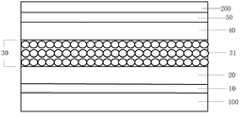
参阅图1所示,量子点发光元件一般包括:在下基板100和上基板200之间设置彼此相对的阳极10和阴极50、以及形成在阳极10和阴极50之间的具有多个量子点31的量子发光层30。其中,在阳极10上形成有由空穴传输粒子构成的空穴传输层20,量子发光层30形成在空穴传输层20上。在量子发光层30上顺序形成有电子传输粒子构成的电子传输层40和阴极50。As shown in FIG. 1 , the quantum dot light-emitting element generally includes: an
现有技术的量子点发光元件的制造过程中,量子点发光层的每一层结构均采用分步或分层制备的方式实现,通常通过溶液工艺在空穴传输层上形成量子点发光层,由于在形成量子点发光层时,用于形成量子点发光层的溶剂会溶解空穴传输层组分,因此量子点发光层下面的空穴传输层的组分也被溶解,从而需要选择在溶液工艺中不能被溶解的材料,因此制备空穴传输层的材料受到限制;此外采用上述制备方法时量子点发光元件的工序较多、工艺复杂,从而造成制造成本很难降低。In the manufacturing process of quantum dot light-emitting elements in the prior art, the structure of each layer of the quantum dot light-emitting layer is realized in a step-by-step or layer-by-layer manner, and the quantum dot light-emitting layer is usually formed on the hole transport layer by a solution process. Since the solvent used to form the quantum dot light-emitting layer will dissolve the hole transport layer components when forming the quantum dot light-emitting layer, the components of the hole transport layer below the quantum dot light-emitting layer are also dissolved, so it is necessary to select Materials that cannot be dissolved in the process, so the materials for preparing the hole transport layer are limited; in addition, when the above preparation method is used, the quantum dot light-emitting element has many procedures and complicated processes, which makes it difficult to reduce the manufacturing cost.
发明内容Contents of the invention
本发明技术方案的目的是提供一种量子点发光元件的制造方法及量子点显示设备,用于简化现有量子点发光元件的制造工序,使量子点发光元件的制造成本降低。The purpose of the technical solution of the present invention is to provide a manufacturing method of a quantum dot light-emitting element and a quantum dot display device, which are used to simplify the manufacturing process of the existing quantum dot light-emitting element and reduce the manufacturing cost of the quantum dot light-emitting element.
本发明提供一种量子点发光元件的制造方法,所述量子点发光元件包括量子点发光层、空穴传输层和电子传输层,其中,所述制造方法包括:The present invention provides a method for manufacturing a quantum dot light-emitting element, the quantum dot light-emitting element includes a quantum dot light-emitting layer, a hole transport layer and an electron transport layer, wherein the manufacturing method includes:
将形成所述量子点发光层的量子点发光材料与形成所述空穴传输层的空穴传输材料混合,或者将形成所述量子点发光层的量子点发光材料与形成所述电子传输层的电子传输材料混合,溶解于有机溶剂中,形成混合溶剂;Mixing the quantum dot luminescent material forming the quantum dot luminescent layer with the hole transport material forming the hole transport layer, or mixing the quantum dot luminescent material forming the quantum dot luminescent layer with the electron transport layer The electron transport material is mixed and dissolved in an organic solvent to form a mixed solvent;
将所述混合溶剂涂覆于所述量子点发光元件的制备基板上;coating the mixed solvent on the preparation substrate of the quantum dot light-emitting element;
除去涂覆有所述混合溶剂的制备基板上的有机溶剂,量子点发光材料与空穴传输材料或者量子点发光材料与所述电子传输材料在所述制备基板上分层,形成所述量子点发光层和所述空穴传输层或者形成所述量子点发光层和所述电子传输层。removing the organic solvent on the prepared substrate coated with the mixed solvent, layering the quantum dot luminescent material and the hole transport material or the quantum dot luminescent material and the electron transport material on the prepared substrate to form the quantum dot The light emitting layer and the hole transport layer or form the quantum dot light emitting layer and the electron transport layer.
优选地,上述所述的制造方法,在将量子点发光材料与空穴传输材料混合并溶解于有机溶剂,形成所述混合溶剂时,将所述混合溶剂涂覆于所述量子点发光元件的制备基板上步骤之前,还包括:Preferably, in the above-mentioned manufacturing method, when the quantum dot luminescent material and the hole transport material are mixed and dissolved in an organic solvent to form the mixed solvent, the mixed solvent is applied to the quantum dot luminescent element. Before preparing the substrate step, also include:
制成所述量子点发光元件的下基板;Making the lower substrate of the quantum dot light-emitting element;
在所述下基板上形成阳极,形成为所述制备基板。An anode is formed on the lower substrate to form the preparation substrate.
优选地,上述所述的制造方法,在形成所述量子点发光层和所述空穴传输层之后还包括:Preferably, the above-mentioned manufacturing method further includes after forming the quantum dot light-emitting layer and the hole transport layer:
在所述量子点发光层的表面沉积电子传输材料,形成为所述电子传输层;Depositing an electron transport material on the surface of the quantum dot light-emitting layer to form the electron transport layer;
在所述电子传输层的表面形成阴极;forming a cathode on the surface of the electron transport layer;
制成所述量子点发光元件的上基板,并使所述上基板与所述阴极连接。The upper substrate of the quantum dot light-emitting element is made, and the upper substrate is connected to the cathode.
优选地,上述所述的制造方法,在将量子点发光材料与电子传输材料混合并溶解于有机溶剂,形成所述混合溶剂时,将所述混合溶剂涂覆于所述量子点发光元件的制备基板上步骤之前,还包括:Preferably, in the above-mentioned manufacturing method, when the quantum dot light-emitting material and the electron transport material are mixed and dissolved in an organic solvent to form the mixed solvent, the mixed solvent is applied to the preparation of the quantum dot light-emitting element Before the on-substrate step, also include:
制成所述量子点发光元件的上基板;Making the upper substrate of the quantum dot light-emitting element;
在所述上基板上形成阴极,形成为所述制备基板。A cathode is formed on the upper substrate to form the preparation substrate.
优选地,上述所述的制造方法,在形成所述量子点发光层与所述电子传输层之后,还包括:Preferably, the above-mentioned manufacturing method, after forming the quantum dot light-emitting layer and the electron transport layer, further includes:
在所述量子点发光层的表面沉积空穴传输材料,形成为所述空穴传输层;Depositing a hole transport material on the surface of the quantum dot light-emitting layer to form the hole transport layer;
在所述空穴传输层的表面形成阳极;forming an anode on the surface of the hole transport layer;
制成所述量子点发光元件的下基板,并使所述下基板与所述阳极连接。The lower substrate of the quantum dot light-emitting element is manufactured, and the lower substrate is connected to the anode.
优选地,上述所述的制造方法,所述下基板上形成有与所述阳极连接的驱动电路,所述上基板上形成有滤光层。Preferably, in the manufacturing method mentioned above, a drive circuit connected to the anode is formed on the lower substrate, and a filter layer is formed on the upper substrate.
优选地,上述所述的制造方法,除去涂覆有所述混合溶剂的制备基板上的有机溶剂的过程包括对所述混合溶剂的加热过程。Preferably, in the above-mentioned manufacturing method, the process of removing the organic solvent on the prepared substrate coated with the mixed solvent includes a process of heating the mixed solvent.
本发明另一方面还提供一种采用如上所述制造方法制成的量子点显示设备,其中,所述量子点显示设备包括量子点发光部分,所述量子点发光部分包括:量子点发光层、空穴传输层和电子传输层。Another aspect of the present invention also provides a quantum dot display device manufactured by the above-mentioned manufacturing method, wherein the quantum dot display device includes a quantum dot light-emitting part, and the quantum dot light-emitting part includes: a quantum dot light-emitting layer, hole transport layer and electron transport layer.
优选地,上述所述的量子点显示设备,还包括:Preferably, the quantum dot display device described above further includes:
下基板,所述下基板上形成有驱动电路;a lower substrate, on which a driving circuit is formed;
阳极,形成于所述下基板上,其中所述空穴传输层、所述量子点发光层和所述电子传输层从所述阳极向上依次形成;an anode formed on the lower substrate, wherein the hole transport layer, the quantum dot light-emitting layer, and the electron transport layer are sequentially formed upward from the anode;
阴极,形成于所述电子传输层上;a cathode formed on the electron transport layer;
上基板,所述上基板上形成有滤光层,所述滤光层与所述阴极连接设置。An upper substrate, a filter layer is formed on the upper substrate, and the filter layer is connected to the cathode.
优选地,上述所述的量子点显示设备,还包括:Preferably, the quantum dot display device described above further includes:
下基板,其中所述下基板上形成有驱动电路和黑色驱阵,所述黑色矩阵将所述下基板划分为多个像素对应区域,每一像素对应区域包括三个子区域;A lower substrate, wherein a driving circuit and a black driving array are formed on the lower substrate, and the black matrix divides the lower substrate into a plurality of pixel-corresponding regions, and each pixel-corresponding region includes three sub-regions;
阳极,形成于每一所述子区域上,所述阳极与所述驱动电路连接;且在每一所述子区域中,所述空穴传输层、所述量子点发光层和所述电子传输层从所述阳极向上依次形成,位于不同子区域上的所述量子点发光层能够发出不同颜色的光;an anode formed on each of the sub-regions, the anode is connected to the driving circuit; and in each of the sub-regions, the hole transport layer, the quantum dot light-emitting layer and the electron transport Layers are formed sequentially upward from the anode, and the quantum dot light-emitting layers located on different sub-regions can emit light of different colors;
阴极,形成于整个所述电子传输层上;a cathode formed over the entire electron transport layer;
上基板,与所述阴极连接设置。The upper substrate is provided in connection with the cathode.
本发明具体实施例上述技术方案中的至少一个具有以下有益效果:At least one of the above technical solutions in specific embodiments of the present invention has the following beneficial effects:
利用量子点发光层上的量子点发光材料与相邻的空穴传输层和电子传输层的电子传输材料粒径尺寸大小的不同,当形成量子点发光层的量子点发光材料与形成空穴传输层的有机分子空穴传输材料或与形成电子传输层的电子传输材料混合并溶解于有机溶剂中时,在除去有机溶剂的过程,上述粒径大小不同的材料能够分层沉积,从而形成量子点发光层和空穴传输层或者形成量子点发光层和电子传输层;因此,所述量子点发光层和所述空穴传输层(或所述电子传输层)通过一步工艺即可制备形成,无需再分层制造,使量子点发光元件的制造工序简化,量子点发光元件的制造成本能够进一步降低;同时还能够改善现有溶液工艺中形成量子点发光层的溶剂对空穴传输层组分的溶解问题。Utilizing the difference in particle size between the quantum dot luminescent material on the quantum dot light-emitting layer and the electron transport material of the adjacent hole transport layer and electron transport layer, when the quantum dot light-emitting material forming the quantum dot light-emitting layer is different from the hole transport material When the organic molecular hole transport material of the layer or the electron transport material forming the electron transport layer is mixed and dissolved in an organic solvent, in the process of removing the organic solvent, the above-mentioned materials with different particle sizes can be layered and deposited to form quantum dots light emitting layer and hole transport layer or form quantum dot light emitting layer and electron transport layer; therefore, said quantum dot light emitting layer and said hole transport layer (or said electron transport layer) can be prepared and formed by one-step process, without Layered manufacturing simplifies the manufacturing process of the quantum dot light-emitting element, and the manufacturing cost of the quantum dot light-emitting element can be further reduced; at the same time, it can also improve the solvent that forms the quantum dot light-emitting layer in the existing solution process. Dissolution problem.
附图说明Description of drawings
图1为现有技术量子点发光元件的一般结构示意图;FIG. 1 is a general structural schematic diagram of a quantum dot light-emitting element in the prior art;
图2为采用本发明第一实施例所述制造方法完成部分工序的结构示意图;Fig. 2 is a structural schematic diagram of part of the process completed by the manufacturing method described in the first embodiment of the present invention;
图3为本发明第一实施例所述制造方法的流程示意图;Fig. 3 is a schematic flow chart of the manufacturing method described in the first embodiment of the present invention;
图4为采用本发明第二实施例所述制造方法完成部分工序的结构示意图;Fig. 4 is a structural schematic diagram of part of the process completed by the manufacturing method described in the second embodiment of the present invention;
图5为采用本发明第二实施例所述制造方法的流程示意图;5 is a schematic flow diagram of the manufacturing method according to the second embodiment of the present invention;
图6为量子点发光层和空穴传输层(或电子传输层)一步工序形成的原理示意图;Figure 6 is a schematic diagram of the principle of one-step formation of the quantum dot light-emitting layer and the hole transport layer (or electron transport layer);
图7为本发明第一实施例所述量子点显示设备的结构示意图;7 is a schematic structural diagram of the quantum dot display device according to the first embodiment of the present invention;
图8为本发明第一实施例所述量子点显示设备采用本发明第一实施例所述制造方法完成部分工序的结构示意图;FIG. 8 is a schematic structural view of the quantum dot display device according to the first embodiment of the present invention using the manufacturing method according to the first embodiment of the present invention to complete part of the process;
图9为本发明第一实施例所述量子点显示设备采用本发明第二实施例所述制造方法完成部分工序的结构示意图;FIG. 9 is a schematic structural view of the quantum dot display device according to the first embodiment of the present invention using the manufacturing method described in the second embodiment of the present invention to complete part of the process;
图10为本发明第二实施例所述量子点显示设备的结构示意图。FIG. 10 is a schematic structural diagram of the quantum dot display device according to the second embodiment of the present invention.
具体实施方式Detailed ways
以下结合附图对本发明的结构和原理进行详细说明,所举实施例仅用于解释和说明本发明保护范围,并非以此限定本发明保护范围。The structure and principle of the present invention will be described in detail below in conjunction with the accompanying drawings. The examples given are only used to explain and illustrate the protection scope of the present invention, not to limit the protection scope of the present invention.
结合图1现有技术量子点发光元件的一般结构示意图,本发明具体实施例所述量子点发光元件的制造方法为利用量子点发光层上的量子点发光材料与相邻的空穴传输层和电子传输材料粒径尺寸大小不同,当形成量子点发光层的量子点发光材料与形成空穴传输层的空穴传输材料或与形成电子传输层的电子传输材料混合并溶解于有机溶剂中时,在除去有机溶剂的过程,上述粒径大小不同的材料能够分层沉积,从而形成量子点发光层和空穴传输层或者形成量子点发光层和电子传输层。In conjunction with the general structural schematic diagram of the quantum dot luminescent element in the prior art in Fig. 1, the manufacturing method of the quantum dot luminescent element described in the specific embodiment of the present invention is to utilize the quantum dot luminescent material on the quantum dot luminescent layer and the adjacent hole transport layer and The particle size of the electron transport material is different. When the quantum dot luminescent material forming the quantum dot luminescent layer is mixed with the hole transport material forming the hole transport layer or with the electron transport material forming the electron transport layer and dissolved in an organic solvent, During the process of removing the organic solvent, the above-mentioned materials with different particle sizes can be layered and deposited to form a quantum dot light emitting layer and a hole transport layer or form a quantum dot light emitting layer and an electron transport layer.
因此,本发明具体实施例所述量子点发光元件的制造方法包括:Therefore, the manufacturing method of the quantum dot light-emitting element described in the specific embodiment of the present invention includes:
将形成所述量子点发光层的量子点发光材料与形成所述空穴传输层的空穴传输材料混合,或者将形成所述量子点发光层的量子点发光材料与形成所述电子传输层的电子传输材料混合,溶解于有机溶剂中,形成混合溶剂;Mixing the quantum dot luminescent material forming the quantum dot luminescent layer with the hole transport material forming the hole transport layer, or mixing the quantum dot luminescent material forming the quantum dot luminescent layer with the electron transport layer The electron transport material is mixed and dissolved in an organic solvent to form a mixed solvent;
将所述混合溶剂涂覆于所述量子点发光元件的制备基板上;coating the mixed solvent on the preparation substrate of the quantum dot light-emitting element;
除去涂覆有所述混合溶剂的制备基板上的有机溶剂,量子点发光材料与空穴传输材料或者量子点发光材料与形成所述电子传输层的电子传输材料在所述制备基板上分层,形成所述量子点发光层和所述空穴传输层或者形成所述量子点发光层和所述电子传输层。removing the organic solvent on the prepared substrate coated with the mixed solvent, layering the quantum dot luminescent material and the hole transport material or the quantum dot luminescent material and the electron transport material forming the electron transport layer on the prepared substrate, Forming the quantum dot light emitting layer and the hole transport layer or forming the quantum dot light emitting layer and the electron transport layer.
采用上述方法,所述量子点发光层和所述空穴传输层(或所述电子传输层)通过一步工艺即可制备形成,无需再分层制造,因此使量子点发光元件的制造工序简化,量子点发光元件的制造成本能够进一步降低。Using the above method, the quantum dot light-emitting layer and the hole transport layer (or the electron transport layer) can be formed through a one-step process without further layered manufacturing, thus simplifying the manufacturing process of the quantum dot light-emitting element, The manufacturing cost of the quantum dot light-emitting element can be further reduced.
此外,所述混合溶剂可以采用旋涂、喷墨或狭缝涂布等通常的溶液涂覆工艺形成在制备基板上,相对于传统的真空蒸镀工艺制备量子点发光层的方式,也能够达到使量子点发光元件的制造工艺简化,量子点发光元件的制造成本进一步降低的目的。In addition, the mixed solvent can be formed on the prepared substrate by common solution coating processes such as spin coating, inkjet or slit coating, compared with the traditional vacuum evaporation process for preparing the quantum dot light-emitting layer, it can also achieve The purpose of simplifying the manufacturing process of the quantum dot light-emitting element and further reducing the manufacturing cost of the quantum dot light-emitting element.
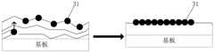
相分离过程主要受两种材料的粒径尺寸和化学特性的影响,量子点发光材料的量子点发光核尺寸较大,如发射白光的量子点发光层由发光核尺寸分别为5.0~5.5nm、3.0~3.5nm、2.0~2.5nm的红色量子点、绿色量子点、蓝色量子点以一定比例混合而成,因此量子点发光核尺寸约为3~10nm,并且量子点表面被烷烃链所包覆,而空穴传输材料(如为四苯基联苯二胺类化合物,N,N′-二苯基-N,N′-二(3-甲苯基)-1,1′-联苯-4,4′-二胺,简称TPD;4,4’-N,N’-二咔唑-联苯,简称CBP;N,N’-二苯基-N,N’-二(1-萘基-1,1’-联苯基-4,4’-二胺),简称a-NPD;4,4’,4’’-三(N-咔唑基)-三苯胺,简称TCA)为芳香族,其分子较小为1nm,因此在将两种材料混合溶解于有机溶剂后,除去有机溶剂的过程中,被烷烃链所包覆的量子点发光材料会与芳香族的空穴传输材料会发生相分离,当使制备基板以涂覆有混合溶剂的表面朝上放置时,量子点发光材料向有机溶剂的上部运动形成覆盖于空穴传输层之上的量子点发光层,空穴传输层形成于量子点发光层的下面,一步工艺实现空穴传输层与量子点发光层的制备。The phase separation process is mainly affected by the particle size and chemical properties of the two materials. The size of the quantum dot luminescent nucleus of the quantum dot luminescent material is relatively large. 3.0-3.5nm, 2.0-2.5nm red quantum dots, green quantum dots, and blue quantum dots are mixed in a certain proportion, so the size of the quantum dot luminescent core is about 3-10nm, and the surface of the quantum dots is covered by alkane chains Covering, while hole transport materials (such as tetraphenylbiphenyl diamine compounds, N,N'-diphenyl-N,N'-bis(3-tolyl)-1,1'-biphenyl- 4,4'-diamine, referred to as TPD; 4,4'-N,N'-dicarbazole-biphenyl, referred to as CBP; N,N'-diphenyl-N,N'-di(1-naphthalene -1,1'-biphenyl-4,4'-diamine), referred to as a-NPD; 4,4',4''-tri(N-carbazolyl)-triphenylamine, referred to as TCA) Aromatic, its molecular size is as small as 1nm. Therefore, after the two materials are mixed and dissolved in an organic solvent, the quantum dot luminescent material covered by the alkane chain will interact with the aromatic hole transport material during the process of removing the organic solvent. Phase separation will occur. When the prepared substrate is placed with the surface coated with the mixed solvent facing up, the quantum dot luminescent material moves to the upper part of the organic solvent to form a quantum dot luminescent layer covering the hole transport layer, and the hole transport The layer is formed under the quantum dot light-emitting layer, and the one-step process realizes the preparation of the hole transport layer and the quantum dot light-emitting layer.
形成电子传输层的电子传输材料可以为TPBI(1,3,5-三(N-苯基苯并咪唑-2-基)苯),TAZ(3-(4-联苯基)-4-苯基-5-叔-丁基苯基-1,2,4-三唑),AlQ3(三(8-羟基喹啉)铝)等有机材料,基于以上相同原理,通过一步工艺也可以实现电子传输层与量子点发光层的制备。The electron transport material that forms electron transport layer can be TPBI (1,3,5-three (N-phenylbenzimidazol-2-yl) benzene), TAZ (3-(4-biphenyl)-4-benzene Based on the same principle as above, electron transport can also be realized by one-step process layer and the preparation of quantum dot light-emitting layer.
本发明实施例所述制造方法中,上述的“制备基板”为在制备形成所述量子点发光层和所述空穴传输层或者制备形成所述量子点发光层和所述电子传输层的工序之前,执行制备量子点发光元件的工序所完成的基板构造,因此并不限于仅包括一透明玻璃基材,也可以包括在透明玻璃基材上形成的阳极以及驱动电路等。In the manufacturing method described in the embodiment of the present invention, the above-mentioned "preparation substrate" refers to the process of preparing and forming the quantum dot light-emitting layer and the hole transport layer or preparing and forming the quantum dot light-emitting layer and the electron transport layer Previously, the substrate structure completed by performing the process of preparing the quantum dot light-emitting element is not limited to only include a transparent glass substrate, but may also include an anode and a driving circuit formed on the transparent glass substrate.
以下结合图1、图2、图3和图6,具体说明本发明第一实施例所述方法,量子点发光层30与空穴传输层20采用一步工艺制成时,量子点发光元件的制备过程,具体包括以下步骤:The method described in the first embodiment of the present invention will be described in detail below in conjunction with FIG. 1, FIG. 2, FIG. 3 and FIG. process, including the following steps:
S110,制成下基板100,通常该下基板100包括一透明玻璃基板;S110, making the
S120,在下基板100上形成具有预定图案的阳极10,形成制备基板;其中采用溅射、蒸镀或旋涂等方法即能够在下基板100上形成该阳极10,本领域技术人员应该了解上述工艺过程,在此不详细描述;S120, forming an
S130,将形成所述量子点发光层的量子点发光材料与形成所述空穴传输层的空穴传输材料溶解于一有机溶剂中,形成混合溶剂,并将混合溶剂涂覆于阳极10的表面;其中可以通过旋涂、喷墨或狭缝涂布等方式进行涂覆,以上涂覆方式为本领域技术人员所熟知的技术,在此不详细描述;S130, dissolving the quantum dot luminescent material forming the quantum dot luminescent layer and the hole transport material forming the hole transport layer in an organic solvent to form a mixed solvent, and coating the mixed solvent on the surface of the
S140,将涂覆有上述混合溶剂的下基板100上的有机溶剂除去,其中该有机溶剂可以为甲苯,除去该有机溶剂的方式可以为加热,随着对下基板100加热过程的进行,有机溶剂蒸发。由于下基板100上所涂覆混合溶剂中的量子点发光材料的粒径尺寸大于空穴传输材料的粒径尺寸,因此量子点材料向上运动,使量子点发光层30形成在空穴传输层20上,该过程原理如图6所示;S140, remove the organic solvent on the
最佳地,对有机溶剂加热的温度为70℃至90℃。Optimally, the temperature for heating the organic solvent is 70°C to 90°C.
除采用以上加热的方式除去混合溶剂中的有机溶液外,也可以采用使混合溶剂在环境温度下自然挥发的方式,完成量子点发光层和空穴传输层的制备分层。In addition to using the above heating method to remove the organic solution in the mixed solvent, the mixed solvent can also be naturally volatilized at ambient temperature to complete the preparation and layering of the quantum dot light-emitting layer and the hole transport layer.
S150,通过溅射、蒸镀或旋涂等方法在量子点发光层30的表面沉积形成电子传输材料,形成为电子传输层40;S150, depositing an electron transport material on the surface of the quantum dot light-emitting
S160,通过溅射、蒸镀或旋涂等方法在电子传输层40表面沉积阴极50;S160, depositing the
S170,制成上基板200,通常该上基板200包括一透明玻璃基板。S170, making the
通过上述的步骤S110至S170,完成如图1所示的量子点发光元件的制备。Through the above steps S110 to S170, the preparation of the quantum dot light-emitting element as shown in FIG. 1 is completed.
以下结合图1、图4、图5与图6,说明本发明第二实施例所述方法,量子点发光层与电子传输层采用一步工艺制成时量子点发光元件的制备过程。1 , 4 , 5 and 6 , the method described in the second embodiment of the present invention, the preparation process of the quantum dot light-emitting element when the quantum dot light-emitting layer and the electron transport layer are made by one-step process will be described below.
S210,制成上基板200;通常该上基板200包括一透明玻璃基板;S210, making the
S220,采用溅射、蒸镀或旋涂等方法在上基板200上形成阴极50;S220, forming the
S230,将形成所述量子点发光层的量子点发光材料与形成所述电子传输层的电子传输材料溶解于一有机溶剂中,形成混合溶剂,并通过旋涂、喷墨或狭缝涂布等方式将混合溶剂涂覆于阴极50的表面;S230, dissolving the quantum dot luminescent material forming the quantum dot luminescent layer and the electron transport material forming the electron transport layer in an organic solvent to form a mixed solvent, and spin coating, inkjet or slit coating, etc. The mixed solvent is coated on the surface of the
S240,将涂覆有上述混合溶剂的上基板200除去其中的有机溶剂,其中除去该有机溶剂的方式可以为加热,随着对上基板200加热过程的进行,有机溶剂蒸发,由于上基板200上所涂覆混合溶剂中的量子点发光材料的粒径大于形成电子传输层的电子传输材料的粒径,因此量子点发光材料向上运动,使量子点发光层30形成在电子传输层40上,如图6所示;S240, remove the organic solvent from the
S250,通过溅射、蒸镀或旋涂等方法在量子点发光层30的表面沉积空穴传输材料,形成为空穴传输层20;S250, depositing a hole transport material on the surface of the quantum dot light-emitting
S260,通过溅射、蒸镀或旋涂等方法在空穴传输层20表面沉积一层阳极10;S260, depositing a layer of
S270,制成下基板100;通常该下基板200包括一透明玻璃基板。S270, making the
通过上述的步骤S210至S270,也能够完成图1所示结构量子点发光元件的制备。Through the above steps S210 to S270, the preparation of the quantum dot light-emitting element with the structure shown in FIG. 1 can also be completed.
本发明上述内容中所提及的“量子点发光元件”可以为一量子点发光二极管也可以为一量子点显示设备,只要为一采用量子点材料发光的元器件均能够采用本发明具体实施例所述方法制备。The "quantum dot light-emitting element" mentioned in the above content of the present invention can be a quantum dot light-emitting diode or a quantum dot display device, as long as it is a component that uses quantum dot materials to emit light, the specific embodiments of the present invention can be used Prepared by the method described.
上述量子点发光元件为一量子点显示设备时,为实现显示设备的彩色图像显示,图1所示结构的下基板100上形成有用于驱动阳极20的驱动电路,上基板200上形成有滤光层。When the above-mentioned quantum dot light-emitting element is a quantum dot display device, in order to realize the color image display of the display device, a driving circuit for driving the
本发明具体实施例另一方面还提供一种采用上述制造方法的量子点显示设备,所述量子点显示设备包括如图1所示结构的量子点发光部分,包括:下基板、阳极、量子点发光层、空穴传输层、电子传输层、阴极和上基板。On the other hand, specific embodiments of the present invention also provide a quantum dot display device using the above-mentioned manufacturing method. The quantum dot display device includes a quantum dot light-emitting part with a structure as shown in Figure 1, including: a lower substrate, an anode, and a quantum dot. Light emitting layer, hole transport layer, electron transport layer, cathode and upper substrate.
图7所示为本发明所述量子点显示设备的第一实施例的结构示意图。FIG. 7 is a schematic structural diagram of the first embodiment of the quantum dot display device of the present invention.
参阅图7所示,第一实施例中,所述量子点显示设备包括下基板100、上基板200以及设置于上基板200与下基板100之间的量子点发光部分,其中:Referring to FIG. 7, in the first embodiment, the quantum dot display device includes a
所述下基板100,包括一透明玻璃基板11,其中该透明玻璃基板11上形成有驱动电路;The
所述量子点发光部分,包括阳极10、空穴传输层20、量子点发光层30、电子传输层40以及阴极50,在从透明玻璃基板11的表面向上顺序设置;The quantum dot light-emitting part, including the
所述下基板200,包括透明玻璃基板21及滤光层22,所述滤光层22包括黑色矩阵及彩膜,形成为多个像素;其中,该滤光层22的结构与普通液晶显示器中滤光层的结构相同。The
利用上述图7所示的量子点显示设备,每一个像素对应的阳极10分别与具有独立驱动功能的薄膜晶体管电路(TFT)相连接(图中未示出),因此每一个像素都可以按照显示器显示画面的要求单独施加不同的电压,以使阳极10和阴极50之间具有不同的电压、电流,因此每一个像素都可以按照画面设定的颜色发出不同亮度光,然后经滤光层22过滤以后混合形成所需显示的画面。图7所示结构的量子点显示设备,采用本发明所述制造方法时,根据本发明所述制造方法的原理,量子点发光层30可以与空穴传输层20采用一步工艺制成,也可以与电子传输层40采用一步工艺制成。Using the quantum dot display device shown in Figure 7 above, the
当量子点发光层30与空穴传输层20采用一步工艺制成时,结合步骤S110至S170以及如图8所示,本发明第一实施例所述量子点显示设备的制造过程包括:When the quantum dot light-emitting
制成下基板100;其中包括在透明玻璃基板11上形成驱动电路;Making the
在下基板100上形成图案化的阳极10,构成为上述的制备基板;A patterned
将形成所述量子点发光层30的量子点发光材料与形成所述空穴传输层20的空穴传输材料溶解于一有机溶剂中,并将混合溶剂涂覆于阳极10的表面;Dissolving the quantum dot luminescent material forming the quantum dot
将涂覆有上述混合溶剂的下基板100除去其中的有机溶剂,其中除去该有机溶剂的方式可以为加热,随着对下基板100加热过程的进行,量子点发光层30形成在空穴传输层20上;Remove the organic solvent from the
通过溅射、蒸镀或旋涂等方法在量子点发光层30的表面沉积形成电子传输材料,形成为电子传输层40;Depositing an electron transport material on the surface of the quantum dot light-emitting
通过溅射、蒸镀或旋涂等方法在电子传输层40表面沉积一层阴极50;Deposit a layer of
制成上基板200,其中包括在透明玻璃基板21上形成滤光层22。The
当量子点发光层30与电子传输层40采用一步工艺制成时,结合步骤S210至S270以及如图9所示,本发明第一实施例所述量子点显示设备的制造过程包括:When the quantum dot light-emitting
制成上基板200,其中包括在透明玻璃基板21上形成滤光层22;Fabricate the
采用溅射、蒸镀或旋涂等方法在上基板200上形成阴极50;Forming the
将形成所述量子点发光层的量子点发光材料与形成所述电子传输层的电子传输材料溶解于一有机溶剂中,形成如图4所示的混合溶剂,并通过旋涂、喷墨或狭缝涂布等方式将混合溶剂涂覆于阴极50的表面;The quantum dot luminescent material forming the quantum dot luminescent layer and the electron transport material forming the electron transport layer are dissolved in an organic solvent to form a mixed solvent as shown in FIG. Coating the mixed solvent on the surface of the
将涂覆有上述混合溶剂的上基板200除去其中的有机溶剂,其中除去该有机溶剂的方式可以为加热,随着对上基板200加热过程的进行,量子点发光层30形成在电子传输层40上;Remove the organic solvent from the
通过溅射、蒸镀或旋涂等方法在量子点发光层30的表面沉积空穴传输材料,形成为空穴传输层20;Depositing a hole transport material on the surface of the quantum dot
通过溅射、蒸镀或旋涂等方法在空穴传输层20表面沉积一层阳极10;Depositing a layer of
制成下基板100,其中包括在透明玻璃基板11上形成驱动电路。The
本领域技术人员应该能够了解在下基板100上形成驱动电路,在上基板200上形成滤光层的具体实现方式,且该部分并非为本发明技术的研究重点,在此不详细描述。Those skilled in the art should be able to understand the specific implementation of forming the driving circuit on the
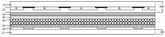
此外,本发明还提供第二实施例的量子点显示设备,参阅图10所示,包括下基板100、上基板200以及设置在两者之间的量子点发光部分,其中:In addition, the present invention also provides the quantum dot display device of the second embodiment, as shown in FIG. 10 , including a
所述下基板100包括:一透明玻璃基板11,该透明玻璃基板11上形成有驱动电路和黑色驱阵111,所述黑色矩阵111将所述下基板划分为多个像素对应区域,每一像素对应区域包括三个子区域;The
阳极10,形成于每一所述子区域上,所述阳极10与所述驱动电路连接;且在每一所述子区域中,所述空穴传输层20、所述量子点发光层30和所述电子传输层40从所述阳极10向上依次形成,位于不同子区域上的所述量子点发光层30能够发出不同颜色的光;An
阴极50,形成于整个所述电子传输层上40;a
上基板200,包括一透明玻璃基板21,与所述阴极50连接设置。The
通过图8所示第二实施例结构的量子点显示设备,利用量子点的特性,当量子点发光核粒径大小不同时,能够发出不同颜色的光,通过在三个不同子区域上设置不同粒径大小的量子点,使不同子区域的所述量子点发光层30能够发出不同颜色的光,最佳地,分别对应发出红色、绿色和蓝色光线,这样无需设置图5所示的滤光层22也能够实现显示设备的RGB三原色的图像显示。Through the quantum dot display device with the structure of the second embodiment shown in Fig. 8, utilizing the characteristics of quantum dots, when the size of quantum dot luminescent core particle size is different, it can emit light of different colors, by setting different colors on three different sub-regions. Quantum dots with particle sizes enable the quantum dot
图10所示结构的量子点显示设备,在采用本发明所述制造方法时,由于量子点发光层30、空穴传输层20和电子传输层40分别被黑色矩阵111划分为多个区域部分,因此上述几层的制备依赖于黑色矩阵111的形成,因此可以仅采用先在下基板100形成黑色矩阵111,形成制备基板,之后在制备基板上使量子点发光层30和空穴传输层20采用一步工艺制备,在此基础上再形成电子传输层40的方式制造,具体可以包括过程:The quantum dot display device with the structure shown in FIG. 10, when using the manufacturing method of the present invention, since the quantum dot light-emitting
制成所述量子点显示设备的下基板100,包括在所述下基板100上依次形成驱动电路和黑色驱阵111,所述黑色矩阵111将下基板100划分为多个像素对应区域,每一像素对应区域包括三个子区域;Making the
在所述下基板100的每一所述子区域上形成阳极10,形成为所述制备基板;forming an
遮挡三个子区域中的其中两个子区域,在剩余一个子区域上涂覆包括有量子点发光材料与空穴传输材料的混合溶剂,其中该子区域上的量子点发光材料用于发出红光;采用同样操作,分别用混合溶剂涂覆另两个子区域,但混合溶剂中的量子点发光材料不同,分别用于发出绿光和蓝光;Blocking two of the three sub-regions, coating the remaining sub-region with a mixed solvent including quantum dot luminescent material and hole transport material, wherein the quantum dot luminescent material on the sub-region is used to emit red light; Using the same operation, the other two sub-regions are coated with mixed solvents, but the quantum dot light-emitting materials in the mixed solvents are different, which are used to emit green light and blue light respectively;
对涂覆有混合溶剂的下基板进行加热,使其中的有机溶剂蒸发,各子区域中的量子点发光层30形成在空穴传输层20上;heating the lower substrate coated with the mixed solvent to evaporate the organic solvent therein, and the quantum dot light-emitting
在每一所述子区域的所述量子点发光层30的表面沉积形成电子传输材料,形成为所述电子传输层40;Depositing and forming an electron transport material on the surface of the quantum dot light-emitting
在整个所述电子传输层40的表面形成阴极50;forming a
制成所述量子点显示设备的上基板200,使所述上基板200与所述阴极50连接。The
因此,图10所示结构的量子点显示设备同样能够采用本发明所述制造方法制备。Therefore, the quantum dot display device with the structure shown in FIG. 10 can also be prepared by the manufacturing method of the present invention.
本发明具体实施例所述制造方法及采用其的量子点显示设备,采用旋涂、喷墨或狭缝涂布等常见的溶液涂覆工艺,将空穴传输材料和量子点发光材料或者将量子点发光材料与形成所述电子传输层的电子传输材料溶解于同一种溶剂中,通过一步工艺即可制备出空穴传输层(电子传输层)与量子点发光层,相对于传统的真空蒸镀以及分层制备的工艺,本发明不仅能够简化制备工艺、降低成本,并且能够制备出致密且均匀的量子点发光层,改善量子点发光层和空穴传输层或电子传输层之间的界面,因此本发明的量子点显示设备具有较低的成本、较高的发光效率、以及较高的色域、亮度等显示品质。The manufacturing method described in the specific embodiments of the present invention and the quantum dot display device using it adopt common solution coating processes such as spin coating, inkjet or slit coating, and the hole transport material and the quantum dot luminescent material or the quantum The dot luminescent material and the electron transport material forming the electron transport layer are dissolved in the same solvent, and the hole transport layer (electron transport layer) and the quantum dot luminescent layer can be prepared through a one-step process. Compared with the traditional vacuum evaporation As well as the process of layered preparation, the present invention can not only simplify the preparation process and reduce the cost, but also can prepare a dense and uniform quantum dot light-emitting layer, improve the interface between the quantum dot light-emitting layer and the hole transport layer or electron transport layer, Therefore, the quantum dot display device of the present invention has lower cost, higher luminous efficiency, and higher display quality such as color gamut and brightness.
以上所述为本发明较佳实施例,应当指出,对于本领域普通技术人员来说,在不脱离本发明保护范围的前提下,还可以作出若干改进和润饰,这些改进和润饰也应视为本发明保护范围。The above description is a preferred embodiment of the present invention. It should be pointed out that for those skilled in the art, some improvements and modifications can also be made without departing from the protection scope of the present invention. These improvements and modifications should also be regarded as The protection scope of the present invention.
Claims (10)
Priority Applications (3)
| Application Number | Priority Date | Filing Date | Title |
|---|---|---|---|
| CN201310367430.2ACN103427049B (en) | 2013-08-21 | 2013-08-21 | Manufacturing method of quantum dot light-emitting component and quantum dot displaying device |
| US14/369,653US20160293875A1 (en) | 2013-08-21 | 2013-12-04 | Method for manufacturing quantum dot light-emitting element and display device using quantum dot |
| PCT/CN2013/088532WO2015024326A1 (en) | 2013-08-21 | 2013-12-04 | Method for manufacturing quantum dot light-emitting element and quantum dot display device |
Applications Claiming Priority (1)
| Application Number | Priority Date | Filing Date | Title |
|---|---|---|---|
| CN201310367430.2ACN103427049B (en) | 2013-08-21 | 2013-08-21 | Manufacturing method of quantum dot light-emitting component and quantum dot displaying device |
Publications (2)
| Publication Number | Publication Date |
|---|---|
| CN103427049Atrue CN103427049A (en) | 2013-12-04 |
| CN103427049B CN103427049B (en) | 2014-12-03 |
Family
ID=49651510
Family Applications (1)
| Application Number | Title | Priority Date | Filing Date |
|---|---|---|---|
| CN201310367430.2AActiveCN103427049B (en) | 2013-08-21 | 2013-08-21 | Manufacturing method of quantum dot light-emitting component and quantum dot displaying device |
Country Status (3)
| Country | Link |
|---|---|
| US (1) | US20160293875A1 (en) |
| CN (1) | CN103427049B (en) |
| WO (1) | WO2015024326A1 (en) |
Cited By (16)
| Publication number | Priority date | Publication date | Assignee | Title |
|---|---|---|---|---|
| CN104051672A (en)* | 2014-07-09 | 2014-09-17 | 深圳市华星光电技术有限公司 | OLED pixel structure |
| CN104299973A (en)* | 2014-09-25 | 2015-01-21 | 京东方科技集团股份有限公司 | Display substrate, preparation method of display substrate and display device |
| WO2015096336A1 (en)* | 2013-12-27 | 2015-07-02 | 京东方科技集团股份有限公司 | Display panel and display device |
| CN105315792A (en)* | 2015-11-18 | 2016-02-10 | Tcl集团股份有限公司 | Quantum dot printing ink and preparation method thereof and quantum dot light-emitting diode |
| CN105336879A (en)* | 2015-10-19 | 2016-02-17 | Tcl集团股份有限公司 | Preparation method for QLED and preparation method for QLED display device |
| CN105655495A (en)* | 2016-03-25 | 2016-06-08 | 深圳市华星光电技术有限公司 | Quantum dot luminescent device, method for preparing quantum dot luminescent device and liquid crystal display device |
| CN105676526A (en)* | 2016-02-18 | 2016-06-15 | 京东方科技集团股份有限公司 | Liquid crystal display panel, manufacturing method thereof and display device comprising liquid crystal display panel |
| CN106356463A (en)* | 2016-10-11 | 2017-01-25 | 深圳市华星光电技术有限公司 | Production method of QLED (Quantum Dot Light Emitting Diode) display device |
| CN108054285A (en)* | 2017-12-12 | 2018-05-18 | 深圳市华星光电技术有限公司 | The preparation method of quantum dot film, electroluminescent device and preparation method thereof |
| WO2018214660A1 (en)* | 2017-05-23 | 2018-11-29 | Tcl集团股份有限公司 | Quantum dot light emitting diode and reverse drive mode thereof |
| CN110161743A (en)* | 2019-05-17 | 2019-08-23 | 京东方科技集团股份有限公司 | A kind of substrate and preparation method thereof, liquid crystal display panel and liquid crystal display device |
| CN110571359A (en)* | 2019-07-31 | 2019-12-13 | 合肥工业大学 | A preparation method of organic molecular doping for improving the performance of CdSe/ZnS quantum dot QLED devices |
| CN112002745A (en)* | 2020-08-25 | 2020-11-27 | 深圳扑浪创新科技有限公司 | Quantum dot color conversion film, preparation method thereof and display panel |
| US11038136B2 (en) | 2018-09-07 | 2021-06-15 | Samsung Electronics Co., Ltd. | Electroluminescent device, and display device comprising thereof |
| CN113614933A (en)* | 2020-03-03 | 2021-11-05 | 东莞市中麒光电技术有限公司 | Light emitting diode and preparation method thereof |
| US11957046B2 (en) | 2018-09-07 | 2024-04-09 | Samsung Electronics Co., Ltd. | Electroluminescent device, and display device comprising thereof |
Families Citing this family (12)
| Publication number | Priority date | Publication date | Assignee | Title |
|---|---|---|---|---|
| US10192932B2 (en)* | 2016-02-02 | 2019-01-29 | Apple Inc. | Quantum dot LED and OLED integration for high efficiency displays |
| US11594698B2 (en)* | 2016-08-23 | 2023-02-28 | Samsung Electronics Co., Ltd. | Electric device and display device comprising quantum dots with improved luminous efficiency |
| KR20180040038A (en)* | 2016-10-11 | 2018-04-19 | 삼성전자주식회사 | Quantum dot light emitting device and optical apparatus including the same |
| KR102783429B1 (en) | 2017-01-25 | 2025-03-18 | 삼성디스플레이 주식회사 | Display device |
| US11342527B2 (en) | 2018-03-29 | 2022-05-24 | Sharp Kabushiki Kaisha | Light-emitting element having commonly formed hole transport layer and anode electrode and light-emitting device |
| KR102087102B1 (en)* | 2018-12-17 | 2020-04-20 | 엘지디스플레이 주식회사 | Organic light emitting pannel and including organic light emitting display |
| US11289557B2 (en) | 2018-12-17 | 2022-03-29 | Lg Display Co., Ltd. | Organic light emitting display panel and organic light emitting display device including the same |
| US11996501B2 (en)* | 2019-02-20 | 2024-05-28 | Sharp Kabushiki Kaisha | Method for manufacturing light-emitting device |
| CN112018249B (en)* | 2019-05-30 | 2024-05-07 | 云谷(固安)科技有限公司 | Light emitting device, manufacturing method thereof and display device |
| CN112331699A (en)* | 2019-12-31 | 2021-02-05 | 广东聚华印刷显示技术有限公司 | Light emitting device, manufacturing method thereof and display device |
| US20230255039A1 (en)* | 2020-07-29 | 2023-08-10 | Sharp Kabushiki Kaisha | Light-emitting device |
| CN114628604A (en)* | 2022-02-25 | 2022-06-14 | 北京京东方技术开发有限公司 | Quantum dot light-emitting device and preparation method thereof, display substrate, and display device |
Citations (3)
| Publication number | Priority date | Publication date | Assignee | Title |
|---|---|---|---|---|
| CN1886844A (en)* | 2003-12-02 | 2006-12-27 | 皇家飞利浦电子股份有限公司 | Electroluminescent device |
| US20090087546A1 (en)* | 2007-09-28 | 2009-04-02 | Dai Nippon Printing Co., Ltd. | Process for producing electroluminescent device |
| CN201796940U (en)* | 2010-09-07 | 2011-04-13 | 上海同天新材料科技有限公司 | Light emitting diode with quantum dots |
Family Cites Families (8)
| Publication number | Priority date | Publication date | Assignee | Title |
|---|---|---|---|---|
| US6770502B2 (en)* | 2002-04-04 | 2004-08-03 | Eastman Kodak Company | Method of manufacturing a top-emitting OLED display device with desiccant structures |
| TWI230798B (en)* | 2004-02-19 | 2005-04-11 | Univ Nat Formosa | Flexible plastic substrate for optical display and producing process |
| US7414294B2 (en)* | 2005-12-16 | 2008-08-19 | The Trustees Of Princeton University | Intermediate-band photosensitive device with quantum dots having tunneling barrier embedded in organic matrix |
| US20080278063A1 (en)* | 2007-05-07 | 2008-11-13 | Cok Ronald S | Electroluminescent device having improved power distribution |
| JP2009087760A (en)* | 2007-09-28 | 2009-04-23 | Dainippon Printing Co Ltd | Method for manufacturing electroluminescence element |
| JP2009087744A (en)* | 2007-09-28 | 2009-04-23 | Dainippon Printing Co Ltd | Light emitting element |
| CN102666369B (en)* | 2009-12-18 | 2014-08-27 | 株式会社村田制作所 | Thin film forming method and quantum dot device |
| KR102038075B1 (en)* | 2012-12-14 | 2019-10-30 | 삼성디스플레이 주식회사 | Organinc light emitting display device and manufacturing method for the same |
- 2013
- 2013-08-21CNCN201310367430.2Apatent/CN103427049B/enactiveActive
- 2013-12-04WOPCT/CN2013/088532patent/WO2015024326A1/enactiveApplication Filing
- 2013-12-04USUS14/369,653patent/US20160293875A1/ennot_activeAbandoned
Patent Citations (3)
| Publication number | Priority date | Publication date | Assignee | Title |
|---|---|---|---|---|
| CN1886844A (en)* | 2003-12-02 | 2006-12-27 | 皇家飞利浦电子股份有限公司 | Electroluminescent device |
| US20090087546A1 (en)* | 2007-09-28 | 2009-04-02 | Dai Nippon Printing Co., Ltd. | Process for producing electroluminescent device |
| CN201796940U (en)* | 2010-09-07 | 2011-04-13 | 上海同天新材料科技有限公司 | Light emitting diode with quantum dots |
Cited By (29)
| Publication number | Priority date | Publication date | Assignee | Title |
|---|---|---|---|---|
| WO2015096336A1 (en)* | 2013-12-27 | 2015-07-02 | 京东方科技集团股份有限公司 | Display panel and display device |
| US9379344B2 (en) | 2013-12-27 | 2016-06-28 | Boe Technology Group Co., Ltd. | Display panel and display device |
| CN104051672B (en)* | 2014-07-09 | 2019-01-01 | 深圳市华星光电技术有限公司 | OLED pixel structure |
| CN104051672A (en)* | 2014-07-09 | 2014-09-17 | 深圳市华星光电技术有限公司 | OLED pixel structure |
| CN104299973A (en)* | 2014-09-25 | 2015-01-21 | 京东方科技集团股份有限公司 | Display substrate, preparation method of display substrate and display device |
| CN104299973B (en)* | 2014-09-25 | 2018-04-06 | 京东方科技集团股份有限公司 | A kind of display base plate and preparation method thereof, display device |
| CN105336879A (en)* | 2015-10-19 | 2016-02-17 | Tcl集团股份有限公司 | Preparation method for QLED and preparation method for QLED display device |
| CN105315792A (en)* | 2015-11-18 | 2016-02-10 | Tcl集团股份有限公司 | Quantum dot printing ink and preparation method thereof and quantum dot light-emitting diode |
| CN105676526B (en)* | 2016-02-18 | 2018-12-25 | 京东方科技集团股份有限公司 | A kind of liquid crystal display panel, its production method and display device |
| CN105676526A (en)* | 2016-02-18 | 2016-06-15 | 京东方科技集团股份有限公司 | Liquid crystal display panel, manufacturing method thereof and display device comprising liquid crystal display panel |
| US10139679B2 (en) | 2016-02-18 | 2018-11-27 | Boe Technology Group Co., Ltd. | Liquid crystal display panel and method of manufacturing the same, and display device |
| CN105655495B (en)* | 2016-03-25 | 2018-05-25 | 深圳市华星光电技术有限公司 | Quantum dot light emitting device and preparation method thereof and liquid crystal display device |
| US9978972B2 (en) | 2016-03-25 | 2018-05-22 | Shenzhen China Star Optoelectronics Technology Co., Ltd | Quantum dot light emitting device and manufacture method thereof and liquid crystal display device |
| CN105655495A (en)* | 2016-03-25 | 2016-06-08 | 深圳市华星光电技术有限公司 | Quantum dot luminescent device, method for preparing quantum dot luminescent device and liquid crystal display device |
| US10263220B2 (en) | 2016-10-11 | 2019-04-16 | Shenzhen China Star Optoelectronics Technology Co., Ltd. | Manufacturing method for QLED display |
| CN106356463A (en)* | 2016-10-11 | 2017-01-25 | 深圳市华星光电技术有限公司 | Production method of QLED (Quantum Dot Light Emitting Diode) display device |
| WO2018214660A1 (en)* | 2017-05-23 | 2018-11-29 | Tcl集团股份有限公司 | Quantum dot light emitting diode and reverse drive mode thereof |
| CN108054285A (en)* | 2017-12-12 | 2018-05-18 | 深圳市华星光电技术有限公司 | The preparation method of quantum dot film, electroluminescent device and preparation method thereof |
| CN108054285B (en)* | 2017-12-12 | 2020-06-05 | 深圳市华星光电技术有限公司 | Preparation method of quantum dot film, electroluminescent device and preparation method thereof |
| US11038136B2 (en) | 2018-09-07 | 2021-06-15 | Samsung Electronics Co., Ltd. | Electroluminescent device, and display device comprising thereof |
| US11957046B2 (en) | 2018-09-07 | 2024-04-09 | Samsung Electronics Co., Ltd. | Electroluminescent device, and display device comprising thereof |
| US12016190B2 (en) | 2018-09-07 | 2024-06-18 | Samsung Electronics Co., Ltd. | Electroluminescent device, and display device comprising thereof |
| CN110161743A (en)* | 2019-05-17 | 2019-08-23 | 京东方科技集团股份有限公司 | A kind of substrate and preparation method thereof, liquid crystal display panel and liquid crystal display device |
| CN110161743B (en)* | 2019-05-17 | 2021-08-10 | 京东方科技集团股份有限公司 | Substrate and preparation method thereof, liquid crystal display panel and liquid crystal display device |
| CN110571359A (en)* | 2019-07-31 | 2019-12-13 | 合肥工业大学 | A preparation method of organic molecular doping for improving the performance of CdSe/ZnS quantum dot QLED devices |
| CN113614933A (en)* | 2020-03-03 | 2021-11-05 | 东莞市中麒光电技术有限公司 | Light emitting diode and preparation method thereof |
| US12068357B2 (en) | 2020-03-03 | 2024-08-20 | Hcp Technology Co., Ltd. | Light emitting diode and preparation method therefor |
| US12191339B2 (en) | 2020-03-03 | 2025-01-07 | Hcp Technology Co., Ltd. | Light emitting diode and manufacturing method therefor |
| CN112002745A (en)* | 2020-08-25 | 2020-11-27 | 深圳扑浪创新科技有限公司 | Quantum dot color conversion film, preparation method thereof and display panel |
Also Published As
| Publication number | Publication date |
|---|---|
| WO2015024326A1 (en) | 2015-02-26 |
| US20160293875A1 (en) | 2016-10-06 |
| CN103427049B (en) | 2014-12-03 |
Similar Documents
| Publication | Publication Date | Title |
|---|---|---|
| CN103427049B (en) | Manufacturing method of quantum dot light-emitting component and quantum dot displaying device | |
| CN105097878B (en) | Organic EL display panel and preparation method, display device | |
| EP3836240A1 (en) | Oled display substrate and manufacturing method therefor, and display apparatus | |
| CN107256879A (en) | Organic electroluminescence display panel and preparation method thereof, organic light-emitting display device | |
| CN104299973B (en) | A kind of display base plate and preparation method thereof, display device | |
| CN108666349B (en) | Color filter substrate, manufacturing method thereof and WOLED display | |
| US20130140533A1 (en) | Pixel structure of electroluminescent display panel | |
| WO2014172951A1 (en) | Organic electroluminescent diode display device | |
| CN106960913A (en) | Light emitting diode with quantum dots display panel and preparation method thereof | |
| CN106531896B (en) | Organic light emitting display device, manufacturing method thereof, and organic light emitting display device | |
| CN105870346B (en) | The manufacturing method and LED display of LED display | |
| JP2001313172A (en) | Organic electroluminescent white light source and method of manufacturing the same | |
| US20030222577A1 (en) | Full color organic light-emitting display device | |
| CN103681773A (en) | Organic electroluminescent display device, preparation method thereof and display device | |
| CN105304681A (en) | Electroluminescent display with organic and inorganic mixed luminescent layer and preparation method of display | |
| TW200932041A (en) | Organic EL display device and method of manufacturing the same | |
| CN105098084B (en) | Quantum dot-based light-emitting diode and display device | |
| WO2018120362A1 (en) | Oled substrate and manufacturing method therefor | |
| CN105704869A (en) | Photochromic and electroluminescent hybrid light emitting display device and fabrication method thereof | |
| CN109037301A (en) | Array substrate and production method, display device | |
| CN106206968B (en) | Pixel structure of OLED display device and preparation method thereof, OLED display device | |
| US20030222576A1 (en) | Full color organic light-emitting display device | |
| CN107180847A (en) | Dot structure, organic electroluminescence display panel and preparation method thereof, display device | |
| CN104681736A (en) | OLED (Organic Light Emitting Diode) unit, manufacturing method of OLED unit and display panel | |
| CN106229418A (en) | A kind of electro-luminescence display device and display device |
Legal Events
| Date | Code | Title | Description |
|---|---|---|---|
| C06 | Publication | ||
| PB01 | Publication | ||
| C10 | Entry into substantive examination | ||
| SE01 | Entry into force of request for substantive examination | ||
| C14 | Grant of patent or utility model | ||
| GR01 | Patent grant |