CN103425316A - Full-plane touch screen panel with single substrate - Google Patents
Full-plane touch screen panel with single substrateDownload PDFInfo
- Publication number
- CN103425316A CN103425316ACN2012103128760ACN201210312876ACN103425316ACN 103425316 ACN103425316 ACN 103425316ACN 2012103128760 ACN2012103128760 ACN 2012103128760ACN 201210312876 ACN201210312876 ACN 201210312876ACN 103425316 ACN103425316 ACN 103425316A
- Authority
- CN
- China
- Prior art keywords
- touch screen
- screen panel
- substrate
- whole plane
- plane touch
- Prior art date
- Legal status (The legal status is an assumption and is not a legal conclusion. Google has not performed a legal analysis and makes no representation as to the accuracy of the status listed.)
- Granted
Links
Images


Classifications
- G—PHYSICS
- G06—COMPUTING OR CALCULATING; COUNTING
- G06F—ELECTRIC DIGITAL DATA PROCESSING
- G06F3/00—Input arrangements for transferring data to be processed into a form capable of being handled by the computer; Output arrangements for transferring data from processing unit to output unit, e.g. interface arrangements
- G06F3/01—Input arrangements or combined input and output arrangements for interaction between user and computer
- G06F3/03—Arrangements for converting the position or the displacement of a member into a coded form
- G06F3/041—Digitisers, e.g. for touch screens or touch pads, characterised by the transducing means
- G06F3/044—Digitisers, e.g. for touch screens or touch pads, characterised by the transducing means by capacitive means
- G06F3/0443—Digitisers, e.g. for touch screens or touch pads, characterised by the transducing means by capacitive means using a single layer of sensing electrodes
- G—PHYSICS
- G06—COMPUTING OR CALCULATING; COUNTING
- G06F—ELECTRIC DIGITAL DATA PROCESSING
- G06F1/00—Details not covered by groups G06F3/00 - G06F13/00 and G06F21/00
- G06F1/16—Constructional details or arrangements
- G06F1/1613—Constructional details or arrangements for portable computers
- G06F1/1633—Constructional details or arrangements of portable computers not specific to the type of enclosures covered by groups G06F1/1615 - G06F1/1626
- G06F1/1637—Details related to the display arrangement, including those related to the mounting of the display in the housing
- G06F1/1643—Details related to the display arrangement, including those related to the mounting of the display in the housing the display being associated to a digitizer, e.g. laptops that can be used as penpads
- G—PHYSICS
- G06—COMPUTING OR CALCULATING; COUNTING
- G06F—ELECTRIC DIGITAL DATA PROCESSING
- G06F1/00—Details not covered by groups G06F3/00 - G06F13/00 and G06F21/00
- G06F1/16—Constructional details or arrangements
- G06F1/1613—Constructional details or arrangements for portable computers
- G06F1/1633—Constructional details or arrangements of portable computers not specific to the type of enclosures covered by groups G06F1/1615 - G06F1/1626
- G06F1/1637—Details related to the display arrangement, including those related to the mounting of the display in the housing
- G06F1/1652—Details related to the display arrangement, including those related to the mounting of the display in the housing the display being flexible, e.g. mimicking a sheet of paper, or rollable
- H—ELECTRICITY
- H01—ELECTRIC ELEMENTS
- H01H—ELECTRIC SWITCHES; RELAYS; SELECTORS; EMERGENCY PROTECTIVE DEVICES
- H01H9/00—Details of switching devices, not covered by groups H01H1/00 - H01H7/00
- H01H9/02—Bases, casings, or covers
- G—PHYSICS
- G06—COMPUTING OR CALCULATING; COUNTING
- G06F—ELECTRIC DIGITAL DATA PROCESSING
- G06F2203/00—Indexing scheme relating to G06F3/00 - G06F3/048
- G06F2203/041—Indexing scheme relating to G06F3/041 - G06F3/045
- G06F2203/04102—Flexible digitiser, i.e. constructional details for allowing the whole digitising part of a device to be flexed or rolled like a sheet of paper
Landscapes
- Engineering & Computer Science (AREA)
- Theoretical Computer Science (AREA)
- Computer Hardware Design (AREA)
- General Engineering & Computer Science (AREA)
- Human Computer Interaction (AREA)
- Physics & Mathematics (AREA)
- General Physics & Mathematics (AREA)
- Position Input By Displaying (AREA)
- Laminated Bodies (AREA)
Abstract
Translated fromChineseDescription
Translated fromChinese技术领域technical field
本发明关于一种触屏(触控)面板,特别关于一种全平面触屏面板。The present invention relates to a touch screen (touch) panel, in particular to a full plane touch screen panel.
背景技术Background technique
各类型的触摸(触控)输入装置已广泛应用于电子产品,例如:行动电话与平板计算机多以触屏(触控)面板作为输入装置,用戶可以方便的将手直接接触输入面板的表面来下达指令,或是在触屏面板的表面游移来操作鼠标或是进行手写文字的输入。与触屏面板搭配的显示面板亦可显示出虚拟按键供用戶点选,用戶可透过这些虚拟按键来输入对应的相关文字。Various types of touch (touch) input devices have been widely used in electronic products. For example, mobile phones and tablet computers mostly use touch screen (touch) panels as input devices. Users can easily touch the surface of the input panel with their hands to Give instructions, or move around on the surface of the touch screen panel to operate the mouse or input handwritten characters. The display panel matched with the touch screen panel can also display virtual buttons for the user to click, and the user can input corresponding relevant text through these virtual buttons.
一般来说,触屏面板一般分为电阻式、电容式、超音波式及红外线式等多种类型,其中又以电阻式触屏面板的产品最多,电阻式触屏面板的设计主要又可区分为四线式、五线式、六线式、八线式等等。四线式触屏面板因为成本及技术层面较为成熟,目前已广泛的生产与应用。Generally speaking, touch screen panels are generally divided into resistive, capacitive, ultrasonic, and infrared types. Among them, resistive touch panels have the most products, and the design of resistive touch panels is mainly divided into Four-wire, five-wire, six-wire, eight-wire and so on. The four-wire touch panel has been widely produced and applied because of its relatively mature cost and technical aspects.
触屏面板包括一基板、在基板上形成的一线路层、绝缘层及软性印刷电路板图案等,然而,基板通常采用透明材质例如玻璃,位于基板边缘的黏接用材料一般为透光材质,故其无法在视觉上遮住绝缘层及软性印刷电路板图案,用戶从基板侧观看触屏面板时仍会看到绝缘层及软性印刷电路板图案。为解决此视觉不美观的问题,传统技术需在壳体额外加上边框,当触屏面板组装于壳体内时,利用边框将触屏面板不欲为人观看到的部份(例如绝缘层及软性印刷电路板图案)遮住,这也造成产品的壳体必须保留额外边框的缺点。The touch screen panel includes a substrate, a circuit layer formed on the substrate, an insulating layer and a flexible printed circuit board pattern, etc. However, the substrate is usually made of a transparent material such as glass, and the bonding material at the edge of the substrate is generally a light-transmitting material , so it cannot visually cover the insulating layer and the pattern of the flexible printed circuit board, and the user will still see the insulating layer and the pattern of the flexible printed circuit board when viewing the touch screen panel from the substrate side. In order to solve this visually unsightly problem, the traditional technology needs to add an additional frame to the housing. When the touch screen panel is assembled in the housing, the part of the touch screen panel that does not want to be viewed by people (such as the insulating layer and the soft layer) The printed circuit board pattern) is covered, which also causes the disadvantage that the product's housing must retain an additional frame.
因此,如何提供一种全平面触屏面板,使其中的边框线路在视觉上不会被用戶察觉,已成为一项重要的课题。Therefore, how to provide a full-plane touch-screen panel in which the frame lines are visually invisible to the user has become an important issue.
发明内容Contents of the invention
本发明的目的为提供一种能够避免边框线路视觉上露出的全平面触屏面板。The purpose of the present invention is to provide a full-plane touch screen panel which can avoid the visual exposure of the frame lines.
此外,本发明另一目的为透过一种新颖的全平面触屏面板设计,使得基板得以兼具多种功能于一体,包括可装饰遮蔽内部线路、保护内侧组件及/或提供完整触摸功能。又,本发明又一目的为提供一种易于与目前现有的电子组件相互整合的全平面触屏面板。In addition, another object of the present invention is to use a novel design of a full-plane touch screen panel, so that the substrate can have multiple functions in one body, including decorating and shielding internal circuits, protecting internal components and/or providing complete touch functions. Furthermore, another object of the present invention is to provide a full-plane touch screen panel that is easy to integrate with existing electronic components.
本发明可采用以下技术方案来实现的。The present invention can be realized by adopting the following technical solutions.
本发明的一种全平面触屏面板包括一基板及多个周边结构。基板具有多个透明导电图案,且各透明导电图案具有一第一端及一第二端。第一端的宽度小于第二端的宽度。周边结构邻设于所述透明导电图案的第一端,且各周边结构具有一第一导电层及一装饰层。第一导电层设置于基板并朝第一端延伸,且覆盖第一端。装饰层设置于基板及第一导电层并朝第一导电层延伸,且在第一导电层上具有一开口。A full-plane touch screen panel of the present invention includes a substrate and a plurality of peripheral structures. The substrate has a plurality of transparent conductive patterns, and each transparent conductive pattern has a first end and a second end. The width of the first end is smaller than the width of the second end. The peripheral structures are adjacent to the first end of the transparent conductive pattern, and each peripheral structure has a first conductive layer and a decoration layer. The first conductive layer is disposed on the substrate, extends toward the first end, and covers the first end. The decoration layer is arranged on the substrate and the first conductive layer and extends toward the first conductive layer, and has an opening on the first conductive layer.
在本发明的一实施例中,透明导电图案的宽度由第二端向第一端渐缩。In an embodiment of the invention, the width of the transparent conductive pattern is tapered from the second end to the first end.
在本发明的一实施例中,装饰层未超过第一导电层的边缘。In an embodiment of the invention, the decoration layer does not exceed the edge of the first conductive layer.
在本发明的一实施例中,透明导电图案的材质包括氧化铟锡,且第一导电层的材质包括碳胶。In an embodiment of the invention, the material of the transparent conductive pattern includes indium tin oxide, and the material of the first conductive layer includes carbon glue.
在本发明的一实施例中,各周边结构还包括一第二导电层。第二导电层设置于装饰层。In an embodiment of the invention, each peripheral structure further includes a second conductive layer. The second conductive layer is disposed on the decoration layer.
在本发明的一实施例中,第二导电层的一部份设置于开口。In an embodiment of the invention, a part of the second conductive layer is disposed in the opening.
在本发明的一实施例中,第二导电层的材质包括银胶、铜、钼或铝。In an embodiment of the invention, the material of the second conductive layer includes silver glue, copper, molybdenum or aluminum.
在本发明的一实施例中,各周边结构还包括一导电填充物。导电填充物设置于装饰层的开口。In an embodiment of the invention, each peripheral structure further includes a conductive filler. The conductive filler is disposed on the opening of the decoration layer.
在本发明的一实施例中,全平面触屏面板还包括一接脚及一导电黏接物。导电黏接物黏接接脚与周边结构的其中之一。In an embodiment of the present invention, the full-plane touch screen panel further includes a pin and a conductive adhesive. The conductive adhesive bonds the pin to one of the surrounding structures.
在本发明的一实施例中,全平面触屏面板还包括一显示模块及一光学胶。光学胶黏接显示模块、基板与周边结构。In an embodiment of the present invention, the full-flat touch screen panel further includes a display module and an optical glue. Optical adhesive bonding display module, substrate and peripheral structure.
在本发明的一实施例中,全平面触屏面板还包括一偏光板。偏光板设置于基板相对于透明导电图案的另一侧。In an embodiment of the present invention, the full plane touch screen panel further includes a polarizer. The polarizing plate is disposed on the other side of the substrate opposite to the transparent conductive pattern.
在本发明的一实施例中,基板兼具触摸感测及盖板的功效。In an embodiment of the present invention, the substrate serves both as a touch sensor and as a cover.
在本发明的一实施例中,全平面触屏面板包括两个基板,且周边结构夹设于基板之间。In an embodiment of the invention, the full-plane touch screen panel includes two substrates, and the peripheral structure is interposed between the substrates.
在本发明的一实施例中,基板可为透明塑料基材、透明玻璃基材、聚酰亚胺(polyimide,PI)或聚对苯二甲酸乙二酯膜状基材。In an embodiment of the present invention, the substrate may be a transparent plastic substrate, a transparent glass substrate, a polyimide (PI) or polyethylene terephthalate film substrate.
在本发明的一实施例中,全平面触屏面板为硬性或可挠性全平面触屏面板。In an embodiment of the present invention, the full flat touch screen panel is a rigid or flexible full flat touch screen panel.
本发明可采用以下技术方案来实现的。The present invention can be realized by adopting the following technical solutions.
为达上述目的,依据本发明的一种全平面触屏面板包括一基板及多个周边结构。基板具有多个透明导电图案,且各透明导电图案具有一第一端及一第二端。第一端的宽度小于第二端的宽度。周边结构分别邻设于所述透明导电图案的其中之一的第一端,且各周边结构具有一第一导电层及一装饰层。装饰层设置于基板并朝第一端延伸。第一导电层设置于装饰层与第一端,并从第一端朝装饰层延伸。To achieve the above purpose, a full-plane touch screen panel according to the present invention includes a substrate and a plurality of peripheral structures. The substrate has a plurality of transparent conductive patterns, and each transparent conductive pattern has a first end and a second end. The width of the first end is smaller than the width of the second end. The peripheral structures are respectively adjacent to the first end of one of the transparent conductive patterns, and each peripheral structure has a first conductive layer and a decoration layer. The decoration layer is arranged on the substrate and extends toward the first end. The first conductive layer is disposed on the decoration layer and the first end, and extends from the first end toward the decoration layer.
在本发明的一实施例中,第一导电层不超过透明导电图案的边缘。In an embodiment of the invention, the first conductive layer does not exceed the edge of the transparent conductive pattern.
在本发明的一实施例中,所述透明导电图案的材质为氧化铟锡,且第一导电层的材质包括高分子导电材料或氧化铟锡。In an embodiment of the present invention, the material of the transparent conductive pattern is indium tin oxide, and the material of the first conductive layer includes a polymer conductive material or indium tin oxide.
在本发明的一实施例中,各周边结构还包括一第二导电层。第二导电层设置于装饰层上朝第一导电层延伸,且未超过第一导电层的边缘。In an embodiment of the invention, each peripheral structure further includes a second conductive layer. The second conductive layer is disposed on the decoration layer and extends toward the first conductive layer, and does not exceed the edge of the first conductive layer.
在本发明的一实施例中,第二导电层的材质包括银胶、铜、钼或铝。In an embodiment of the invention, the material of the second conductive layer includes silver glue, copper, molybdenum or aluminum.
在本发明的一实施例中,全平面触屏面板还包括一接脚及一导电黏接物。导电黏接物黏接接脚与周边结构的其中之一。In an embodiment of the present invention, the full-plane touch screen panel further includes a pin and a conductive adhesive. The conductive adhesive bonds the pin to one of the surrounding structures.
在本发明的一实施例中,全平面触屏面板还包括一显示模块及一光学胶。光学胶黏接显示模块、基板与周边结构。In an embodiment of the present invention, the full-flat touch screen panel further includes a display module and an optical glue. Optical adhesive bonding display module, substrate and peripheral structure.
在本发明的一实施例中,透明导电图案的宽度由第二端向第一端渐缩。In an embodiment of the invention, the width of the transparent conductive pattern is tapered from the second end to the first end.
在本发明的一实施例中,全平面触屏面板还包括一偏光板。偏光板设置于基板相对于透明导电图案的另一侧。In an embodiment of the present invention, the full plane touch screen panel further includes a polarizer. The polarizing plate is disposed on the other side of the substrate opposite to the transparent conductive pattern.
在本发明的一实施例中,基板兼具触摸感测及盖板的功效。In an embodiment of the present invention, the substrate serves both as a touch sensor and as a cover.
在本发明的一实施例中,全平面触屏面板包括两个基板,且周边结构夹设于基板之间。In an embodiment of the invention, the full-plane touch screen panel includes two substrates, and the peripheral structure is interposed between the substrates.
在本发明的一实施例中,基板可为透明塑料基材、透明玻璃基材或聚对苯二甲酸乙二酯膜状基材。In an embodiment of the present invention, the substrate may be a transparent plastic substrate, a transparent glass substrate or a polyethylene terephthalate film substrate.
在本发明的一实施例中,全平面触屏面板为硬性或可挠性全平面触屏面板。In an embodiment of the present invention, the full flat touch screen panel is a rigid or flexible full flat touch screen panel.
承上所述,本发明的全平面触屏面板通过第一导电层设置于基板并朝第一端延伸,且覆盖第一端,而装饰层设置于基板并朝第一导电层延伸,或装饰层设置于基板并朝第一端延伸,且第一导电层设置于装饰层与第一端,从而使得装饰层能够遮蔽边框线路,使得用户在视觉上不会直接观看到边框线路。此外,利用本发明的全平面触屏面板,可以仅使用单片基板,进而免除额外使用透明接着胶或盖板的需要,利于产品薄型化。Based on the above, the full-plane touch screen panel of the present invention is arranged on the substrate and extends toward the first end through the first conductive layer, and covers the first end, and the decoration layer is arranged on the substrate and extends toward the first conductive layer, or the decorative layer The layer is disposed on the substrate and extends toward the first end, and the first conductive layer is disposed on the decoration layer and the first end, so that the decoration layer can shield the frame circuit, so that the user cannot directly observe the frame circuit visually. In addition, by using the full-plane touch screen panel of the present invention, only a single substrate can be used, thereby eliminating the need for additional use of transparent adhesive or cover plate, which is beneficial to thinning the product.
更重要且有利的是,依据本发明的全平面触屏面板,其基板可兼具多种功能于一体,是为已知技术中所不能达成的。其一是可以提供装饰功能,以遮蔽周边结构、边框线路或其它内部组件;其二是保护透明导电图案、周边结构、边框线路或其它内部组件不受损害;其三是可供设置透明导电图案,以提供触摸感测功能。总和而言,虽然已知技术可以加设盖板的方式而有前述的装饰及保护两项效果,但需要额外的制程及材料,反观本发明透过新颖的设计,实现了多功能基板的概念,又因为单一个基板的功能增强,免除了面板内另一个基板的需求,以及简化其它为达装饰或保护目的而增加的额外贴合或组装步骤,故适合模块化的制程,有利成本的降低。More importantly and advantageously, according to the full-plane touch screen panel of the present invention, the substrate thereof can combine multiple functions into one body, which cannot be achieved in the known technology. One is to provide a decorative function to cover the surrounding structure, frame line or other internal components; the other is to protect the transparent conductive pattern, surrounding structure, frame line or other internal components from damage; the third is to set the transparent conductive pattern , to provide touch sensing functionality. In summary, although the known technology can add a cover plate to achieve the aforementioned two effects of decoration and protection, it requires additional manufacturing processes and materials. In contrast, the present invention realizes the concept of a multifunctional substrate through a novel design , and because the enhanced function of a single substrate eliminates the need for another substrate in the panel, and simplifies other additional bonding or assembly steps for decorative or protective purposes, it is suitable for modular manufacturing processes and is beneficial to cost reduction .
此外,透过本发明结构,可通过包括宽度渐缩的第一导电层在内的特征,使全平面触屏面板可与目前现有效能略差的驱动芯片及运算单元兼容,提升应用性。In addition, through the structure of the present invention, through the features including the first conductive layer with tapered width, the full-plane touch panel can be compatible with the currently existing driver chips and computing units with slightly lower performance, thereby improving applicability.
附图说明Description of drawings
图1A至图1F为本发明优选实施例的一种全平面触屏面板的示意图;1A to 1F are schematic diagrams of a full-plane touch screen panel according to a preferred embodiment of the present invention;
图2为本发明优选实施例的另一种全平面触屏面板的示意图;2 is a schematic diagram of another full-plane touch screen panel according to a preferred embodiment of the present invention;
图3A至图3F为本发明优选实施例的一种全平面触屏面板的示意图;3A to 3F are schematic diagrams of a full-plane touch screen panel in a preferred embodiment of the present invention;
图4为本发明优选实施例的另一种全平面触屏面板的示意图;4 is a schematic diagram of another full-plane touch screen panel according to a preferred embodiment of the present invention;
图5A及图5B分别为本发明优选实施例的又一全平面触屏面板的示意图;以及FIG. 5A and FIG. 5B are respectively schematic diagrams of another full-plane touch screen panel according to a preferred embodiment of the present invention; and
图6A及图6B为本发明不同实施例的一种全平面触屏面板的示意图。6A and 6B are schematic diagrams of a full-plane touch screen panel according to different embodiments of the present invention.
主要元件符号说明:Description of main component symbols:
1、1a、2、3、3a、4、6a、6b:全平面触屏面板1, 1a, 2, 3, 3a, 4, 6a, 6b: Full flat touch panel
11、11a、31、31a、61a、61b:基板11, 11a, 31, 31a, 61a, 61b: Substrate
111、111a、311、311a、611a、611b:透明导电图案111, 111a, 311, 311a, 611a, 611b: transparent conductive pattern
112、162、312、362:光学膜112, 162, 312, 362: optical film
12、32、62a、62b:周边结构12, 32, 62a, 62b: Surrounding structures
121、121a、321、321a、41:第一导电层121, 121a, 321, 321a, 41: first conductive layer
122、122a、322、322a:装饰层122, 122a, 322, 322a: decorative layer
123、123a、323、323a:第二导电层123, 123a, 323, 323a: second conductive layer
13、13a、33、33a:绝缘层13, 13a, 33, 33a: insulating layer
14、34:接脚14, 34: pin
15、15a、35、35a:导电黏接物15, 15a, 35, 35a: Conductive adhesive
16、36:显示模块16, 36: display module
161、361、18、38:偏光板161, 361, 18, 38: polarizer
17、37:光学胶17, 37: optical glue
21:导电填充物21: Conductive filler
E1:第一端E1: first end
E2:第二端E2: second end
H:开口H: open
S1:外表面S1: Outer surface
S2:内表面S2: inner surface
具体实施方式Detailed ways
以下将参照相关附图,说明依本发明优选实施例的一种全平面触屏面板,其中相同的元件将以相同的元件符号加以说明。A full-flat touch screen panel according to a preferred embodiment of the present invention will be described below with reference to related drawings, wherein the same components will be described with the same reference numerals.
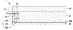
首先,请参照图1A至图1F,其为本发明优选实施例的一种全平面触屏面板1的示意图。如图1A及图1B所示,全平面触屏面板1包括一基板11及多个周边结构12,由于仅具有单一基板11,故可称为具单基板的全平面触屏面板。基板11为一透明基材,例如是透明塑料基材或透明玻璃基材,另外,基板11也可以是聚对苯二甲酸乙二酯膜状基材。基板11的外表面S1供用户操作,用户通常从外表面S1观看全平面触屏面板1并于外表面S1进行操作,全平面触屏面板1的其余结构及组件则设置于基板11的内表面S2一侧。First of all, please refer to FIG. 1A to FIG. 1F , which are schematic diagrams of a full-flat touch screen panel 1 according to a preferred embodiment of the present invention. As shown in FIG. 1A and FIG. 1B , the full-planar touch screen panel 1 includes a
基板11的内表面S2具有多个透明导电图案111,且透明导电图案111用以定义出触摸(触控)感应线路,其材质例如是氧化铟锡(IndiumTin Oxide,ITO)。各透明导电图案111具有一第一端E1及一第二端E2,且相邻的透明导电图案111的设置方向为镜像设置的关系。各透明导电图案111的宽度是由第二端E2向第一端E1渐缩,且第一端E1的宽度是小于第二端E2的宽度。The inner surface S2 of the
在本实施例中,是以透明导电图案111的数量为五个,且其外观是三角形为例进行说明,然而并非以此为限。在实际运用时,透明导电图案111的数量及其形状,将可依据全平面触屏面板1的尺寸及设计上的考虑,而有不同的选择。In this embodiment, it is illustrated by taking five transparent
周边结构12是分别邻设于透明导电图案111的第一端E1,且各周边结构12具有一第一导电层121及一装饰层122。第一导电层121设置于基板11并朝透明导电图案111的第一端E1延伸,且覆盖第一端E1。装饰层122设置于基板11及第一导电层121并朝第一导电层121延伸,且在第一导电层121上具有一开口H。此外,装饰层122的设置位置并未超过第一导电层121的边缘。换句话说,装饰层122的投影是落在于第一导电层121,或与第一导电层121的边缘齐平。The
第一导电层121的材质包括具导电性的碳胶,装饰层122的材质例如是绝缘材料或具备绝缘性的各种颜色油墨(Ink),在装饰层122的颜色的选择上,较佳的是选用与第一导电层121的颜色相似的颜色。因而,用户从外表面S1观看全平面触屏面板1将较不易察觉到装饰层122与第一导电层121之间的颜色变化。其中,第一导电层121及装饰层122可通过印刷的方式形成于基板11上。The material of the first
接着,如图1C所示,周边结构12包括一第二导电层123。第二导电层123设置于装饰层122,且其一部份填入于开口H并与第一导电层121电性连接。第二导电层123的材质可包括银胶、铜、钼或铝。在实施上,若第二导电层123包括银胶时,其可经由网印设备搭配细线路的网版而定义出细线路,并印刷于装饰层122上。此外,若第二导电层123的材质包括铜、钼或铝时,则可经由溅镀制程形成铜导线或钼铝导线。Next, as shown in FIG. 1C , the
值得一提的是,在本发明中当涉及印刷制程时,可采用例如是凸版印刷、凹版印刷、平版印刷或网版印刷等印刷方式而形成,本发明于此并不加以限定,例如第一导电层121、装饰层122及第二导电层123均可采用上述各式印刷方式。此外,当第二导电层123包括银胶时,前述的银胶可包括奈米银粒子,且银胶还可包括其它的导电金属,例如是钛、锌、锆、锑、铟、锡、铜、钼或铝,以进一步强化导电性能。It is worth mentioning that when the printing process is involved in the present invention, printing methods such as letterpress printing, gravure printing, offset printing or screen printing can be used to form, and the present invention is not limited here. For example, the first The
此外,第二导电层123的印刷方式还可以进一步与微影制程配合。具体来说,第二导电层123的图案可采用感光型导电物质或辐射固化导电物质作为印刷材料,并以上述的印刷方式印制于基板11,较佳的是以网版印刷方式进行印制;其后,使用例如紫外光等电磁波辐射,并搭配光罩的遮蔽,以固化部分的感光型导电物质或辐射固化导电物质;接着,当清洗或蚀刻未固化的部分后,即可形成所需的图案,在实施上,可通过例如是纯水,以将未固化的感光型导电物质或辐射固化导电物质移除,而使已固化的感光型导电物质或辐射固化导电物质形成所需的特定图案的第二导电层123。In addition, the printing method of the second
进一步而言,上述的感光型导电物质或辐射固化导电物质并不限制于特殊的成份组成,而可为任一种具有一定导电特性,且受到光线照射,特别是短波长辐射照射后,其性质会产生干燥或固化的物质,且重要的是,以此作法能使第二导电层123形成线宽较小、线距较窄的细导电线路。Further, the above-mentioned photosensitive conductive material or radiation-curable conductive material is not limited to a specific composition, but can be any one with certain conductive properties, and its properties can be improved after being irradiated by light, especially short-wavelength radiation. A dry or solidified substance will be produced, and importantly, the second
如图1D所示,全平面触屏面板1还包括一绝缘层13、一接脚14及一导电黏接物15。绝缘层13设置于第二导电层123上,导电黏接物15黏接接脚14与第二导电层123。在实施上,绝缘层13可透过网版印刷的方式覆盖于第二导电层123上,借以避免第二导电层123因暴露于空气中而形成氧化。接脚14例如是一软性印刷电路板(Flexible Printed Circuit Board,FPC)的接脚,其通过导电黏接物15黏着固定于第二导电层123上,并邻设于绝缘层13。接脚14透过导电黏接物15及第二导电层123而与第一导电层121电性连接,从而接收透明导电图案111所产生的触摸感应讯号。其中,导电黏接物15可为异方性导电膜(Anisotropic Conductive Film,ACF)或异方性导电胶(AnisotropicConductive Paste,ACP)。当然,在其它实施例中亦可不设置绝缘层,本发明在此不限。As shown in FIG. 1D , the full-flat touch screen panel 1 further includes an insulating
接着,如图1E所示,全平面触屏面板1还包括一显示模块16及一光学胶17。在实施上,显示模块16包括一液晶显示模块及一偏光板。光学胶17用以黏接显示模块16、基板11与周边结构12。Next, as shown in FIG. 1E , the full-flat touch screen panel 1 further includes a
因此,通过上述的结构,本发明将可透过选用颜色相似的第一导电层121及装饰层122,以及将第二导电层123设置于装饰层122上,从而使得由第一导电层121、第二导电层123、导电黏接物15与接脚14所构成的边框线路,在视觉上不会被用户察觉。其次,本发明透过将透明导电图案111直接形成于基板11上,还使得基板11兼具触摸感测及盖板的功效,而利于产品的薄型化。此外,由于第一导电层121是直接设置于基板11并与第一端E1连接,将不易因周边结构12的高度的影响而发生断线的状况,从而提升全平面触屏面板1的讯号传递的可靠度。Therefore, through the above-mentioned structure, the present invention can select the first
另外,如图1F所示,全平面触屏面板1的显示模块16除同前述而可具有一偏光板161外,另外还可具有一光学膜162。其中,偏光板161可为轴向偏光板,且光学膜162可例如具有1/4λ的位相差补偿功能。此外,全平面触屏面板1在基板11的外侧同样可贴合一光学膜112,其也可具有例如1/4λ的位相差补偿功能,以与光学膜162配合,使射入的光线能在圆光与线光间适当的转换。全平面触屏面板1还包括另一偏光板18,且较佳的,偏光板18也是为轴向偏光板。偏光板18可设置于基板11相对于透明导电图案的另一侧111,也就是用户进行触摸操作或直接观看的一侧。In addition, as shown in FIG. 1F , the
在实施上,当基板11为聚碳酸脂薄膜(PC film),且由操作或直接观看的一侧向内依序具有偏光板18、具有1/4λ的位相差补偿特性的光学膜112以及显示模块16的光学膜162与偏光板161时,一方面可以防止光学干涉纹路或图形产生,另一方面也可以加强在强光环境下的可视程度,例如太阳光下的可视程度。当然,在其它实施例中,光学膜112或光学膜162也可以透过在基板11或显示模块16内的结构上涂布位相差涂层来取代。In practice, when the
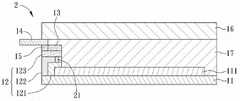
接着,请参照图2,其为本发明优选实施例的另一种全平面触屏面板2的示意图。全平面触屏面板2与全平面触屏面板1的区别在于,全平面触屏面板2还具有一导电填充物21,且导电填充物21是设置于装饰层122的开口H(请参照图1B所示),而第二导电层123是设置于装饰层122及导电填充物21上。其中,导电填充物21的材质例如但不限于碳、奈米铜、奈米银、或高分子导电树脂等等。Next, please refer to FIG. 2 , which is a schematic diagram of another full-flat
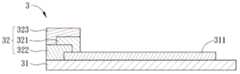
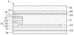
请参照图3A至图3F,其为本发明优选实施例的一种全平面触屏面板3的示意图。如图3A及图3B所示,全平面触屏面板3包括一基板31及多个周边结构32。基板31为一透明基板,例如是塑料基板或玻璃基板。基板31具有一外表面S1及一内表面S2。用户通常从外表面S1观看全平面触屏面板3并于外表面S1进行操作,全平面触屏面板3的其余结构及组件则设置于基板31的内表面S2一侧。Please refer to FIG. 3A to FIG. 3F , which are schematic diagrams of a full-flat
基板31的内表面S2具有多个透明导电图案311,且透明导电图案311定义出触摸感应线路,且其材质例如是氧化铟锡。各透明导电图案311具有一第一端E1及一第二端E2。各透明导电图案311的宽度是由第二端E2向第一端E1渐缩,且第一端E1的宽度是小于第二端E2的宽度。在本实施例中,是以透明导电图案311的数量为五个,且其外观是梯形为例进行说明,然而并非以此为限。The inner surface S2 of the
周边结构32是分别邻设于透明导电图案311的第一端E1,且各周边结构32具有一第一导电层321及一装饰层322。装饰层322设置于基板31并朝第一端E1延伸,第一导电层321设置于装饰层322与第一端E1,并从第一端E1朝装饰层322延伸,而超过透明导电图案311的边缘。其中,第一导电层321的材质包括高分子导电材料或氧化铟锡,且其可利用印刷方式形成。The
接着,如图3C所示,全平面触屏面板3还包括一第二导电层323。第二导电层323设置于装饰层322与第一导电层321,并朝第一导电层321延伸,且未超过第一导电层321的边缘。换句话说,第二导电层323的投影是落在于第一导电层321,或与第一导电层321的边缘切齐。第二导电层323的材质可包括银胶,其可经由网印设备搭配细线路的网版而定义出细线路,并印刷于装饰层322上。另外,第二导电层323的材质可包括铜、钼、铝等金属,其可经由溅镀制程形成铜导线或钼铝导线。Next, as shown in FIG. 3C , the full-plane
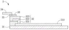
如图3D所示,全平面触屏面板3还包括一绝缘层33、一接脚34及一导电黏接物35。绝缘层33设置于第二导电层323上,导电黏接物35黏接接脚34与第二导电层323。在实施上,绝缘层33可透过网版印刷的方式覆盖于第二导电层323上,借以避免第二导电层323因暴露于空气中而形成氧化。接脚34例如是一软性印刷电路板(Flexible Printed Circuit Board,FPC)的接脚,其通过导电黏接物35黏着固定于第二导电层323上。接脚34透过导电黏接物35及第二导电层323而与第一导电层321电性连接,从而接收透明导电图案311所产生的触摸感应讯号。其中,导电黏接物35可为异方性导电膜或异方性导电胶。当然,同样的,在其它实施例中亦可不设置绝缘层,本发明在此不限。As shown in FIG. 3D , the full-flat
接着,如图3E所示,全平面触屏面板3还包括一显示模块36及一光学胶37。在实施上,显示模块36包括一液晶显示模块及一偏光板。光学胶37用以黏接显示模块36、基板31与周边结构32。Next, as shown in FIG. 3E , the full-flat
因此,通过上述的结构,本发明可透过将装饰层322设置于基板31,以及将第一导电层321设置于装饰层322上,从而使得由第一导电层321、第二导电层323、导电黏接物35与接脚34所构成的边框线路,在视觉上不会被用户察觉。Therefore, through the above-mentioned structure, the present invention can arrange the
其次,通过将透明导电图案311直接形成于基板31上,使得基板31具有触摸感测功能,进而与前述相同,基板31可具有三重功用,一是供形成透明导电图案311,以用于触摸感测;二是直接作为保护体;三是遮蔽装饰周边结构32或其它边框或内部线路及组件,利于产品的薄型化。Secondly, by directly forming the transparent
又如图3F所示,全平面触屏面板3如前述全平面触屏面板1,还可包括偏光板361、38以及光学膜362、312,以防止光学干涉纹路或图形产生,并同时加强在强光环境下的可视程度。其中,由于偏光板361、38以及光学膜362、312的特性与前述实施例的偏光板161、18以及光学膜162、112大致相同,故于此不再赘述。As shown in FIG. 3F, the full-flat
需再次强调的是,在前述多个使用单一基板的全平面触屏面板实施例中,由于单片基板上设置有功能完整的透明导电图案,基板可兼具多种功能于一体。其一,当组装完成后,基板位于外表面,覆盖于周边结构、边框线路、透明导电图案及其它组件上,故一方面可以提供装饰功能,以遮蔽周边结构、边框线路或其它内部组件,避免外露而被察觉;另一方面也可以保护周边结构、边框线路及透明导电图案不受损害。再加上基板上有完整的透明导电图案,足以提供感测功能。是故,本发明实现了基板制程简单化且功能多样化的目标,属于前瞻性的概念创作,并免除了额外再贴合一遮蔽结构的步骤,适合模块化的制程,有利成本的降低。并在上述的概念下,本发明并无其它的限制,而涵盖以实质上相同或相似的任一制程或结构所形成的不同态样的全平面触屏面板。It should be emphasized again that in the above-mentioned embodiments of full-plane touch screen panels using a single substrate, since the transparent conductive pattern with complete functions is disposed on the single substrate, the substrate can have multiple functions in one body. First, when the assembly is completed, the substrate is located on the outer surface and covers the surrounding structures, frame lines, transparent conductive patterns and other components, so on the one hand it can provide a decorative function to cover the surrounding structures, frame lines or other internal components to avoid On the other hand, it can also protect the surrounding structures, frame lines and transparent conductive patterns from damage. Coupled with a complete transparent conductive pattern on the substrate, it is sufficient to provide sensing functions. Therefore, the present invention achieves the goal of simplifying the substrate manufacturing process and diversifying functions, which is a forward-looking concept creation, and eliminates the additional step of attaching a masking structure, which is suitable for a modular manufacturing process and is beneficial to cost reduction. And under the above concepts, the present invention has no other limitations, but covers full-plane touch screen panels of different styles formed by any process or structure that is substantially the same or similar.
值得一提的是,在以上实施例中,当基板11、31为膜片(膜状)基材时,触屏面板可为可挠性触屏面板(或称可挠式触屏面板)。若基板11、31为玻璃基材时,触屏面板可为一硬性触屏面板(或称硬式触屏面板),当然,若基板11、31为软性玻璃,触屏面板还具有可挠性。It is worth mentioning that, in the above embodiments, when the
换言之,若以基板11、31的材质及其所呈现的特性进行区分,本发明的全平面触屏面板可以是硬性(式)全平面触屏面板或可挠性(式)全平面触屏面板。In other words, if the materials of the
接着,请参照图4所示,其为本发明优选实施例的另一种全平面触屏面板4的示意图。全平面触屏面板4与全平面触屏面板3的区别在于,全平面触屏面板4的第一导电层41并未超过透明导电图案311的边缘。换句话说,第一导电层41的投影是落在透明导电图案311上。Next, please refer to FIG. 4 , which is a schematic diagram of another full-plane touch screen panel 4 according to a preferred embodiment of the present invention. The difference between the full plane touch screen panel 4 and the full plane
此外,值得另外说明的是,依据上述实施例的结构,其通过包括宽度渐缩的第一导电层在内的特征,使本发明的全平面触屏面板可与目前的驱动芯片及运算单元兼容,特别是效能略差的兼容,因而利于与当前的电子组件相互整合,进而提升其应用性。In addition, it is worth explaining that, according to the structure of the above-mentioned embodiment, the full-flat touch screen panel of the present invention is compatible with the current driver chip and computing unit through the features including the first conductive layer with tapered width. , especially those with slightly lower performance, which is conducive to the mutual integration with current electronic components, thereby improving its applicability.
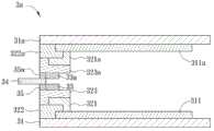
图5A及图5B分别为本发明优选实施例的又一全平面触屏面板的示意图。请先参考图5A所示,全平面触屏面板1a包括基板11、11a、透明导电图案111、111a、第一导电层121、121a、装饰层122、122a、第二导电层123、123a、绝缘层13、13a、接脚14以及导电黏接物15、15a。由于基板11a、透明导电图案111a、第一导电层121a、装饰层122a、第二导电层123a、绝缘层13a、接脚14以及导电黏接物15a与前述图1A至1D的对应组件具有类似的结构及制造过程,故此不再赘述细节。5A and 5B are schematic diagrams of yet another full-plane touch screen panel according to a preferred embodiment of the present invention. Please refer to FIG. 5A first, the full-plane touch screen panel 1a includes
又再参考图5B所示,全平面触屏面板3a包括基板31、31a、透明导电图案311、311a、第一导电层321、321a、装饰层322、322a、第二导电层323、323a、绝缘层33、33a、接脚34以及导电黏接物35、35a。由于基板31a、透明导电图案311a、第一导电层321a、装饰层322a、第二导电层323a、绝缘层33a、接脚34以及导电黏接物35a与前述图3A至3D的对应组件具有类似的结构及制造过程,故此不再赘述细节。Referring again to FIG. 5B, the full-plane
惟要说明的是,上述两种全平面触屏面板可说明本发明亦可应用于双层基材结构,应用范围不受限。具体而言,全平面触屏面板在原有单一基板外,可加设另一基板,且周边结构夹设于基板之间,故即便于双层基材结构中,接近用户操作一侧的基板亦具有三重功用,除可兼具装饰以及保护周边结构、边框线路或其它组件不受损害的功能外,亦可提供例如一轴向上的触摸感测功能,换言的,为一种多功能基板。It should be noted that the above two types of full-flat touch screen panels can illustrate that the present invention can also be applied to a double-layer substrate structure, and the scope of application is not limited. Specifically, in addition to the original single substrate of the full-flat touch screen panel, another substrate can be added, and the surrounding structure is sandwiched between the substrates, so even in the double-layer substrate structure, the substrate on the side close to the user's operation is also It has a triple function. In addition to the functions of decoration and protection of surrounding structures, frame lines or other components from damage, it can also provide, for example, an axial touch sensing function. In other words, it is a multifunctional substrate. .
又,图6A及图6B为本发明不同实施例的一种全平面触屏面板的示意图。在此两个实施例中,全平面触屏面板6a、6b与前述实施例所揭示的大致相同,亦具有基板61a、61b、透明导电图案611a、611b、周边结构62a、62b,且第一端E1的宽度小于第二端E2的宽度。惟不同处在于,图6A所示的透明导电图案611a的形状实质上呈直角三角形状,而图6B所示的透明导电图案611b的形状实质上呈梯型形状。据此可知,依据本发明的透明导电图案不已特定形状为限,端视符合第一端的宽度小于第二端的宽度的概念即可,而亦涵盖其它实质意义上相同或相似的图案。6A and 6B are schematic diagrams of a full-plane touch screen panel according to different embodiments of the present invention. In these two embodiments, the full-plane
在上述的实施例中,基板11a、31a、61a、61b为一透明基材,例如是透明塑料基材、透明玻璃基材、聚酰亚胺(polyimide,PI)或聚对苯二甲酸乙二酯膜状基材。In the above-mentioned embodiments, the
综上所述,本发明的全平面触屏面板通过第一导电层设置于基板并朝第一端延伸,且覆盖第一端,而装饰层设置于基板并朝第一导电层延伸,或装饰层设置于基板并朝第一端延伸,且第一导电层设置于装饰层与第一端,从而使得装饰层能够遮蔽边框线路,以使得用户在视觉上不会直接观看到边框线路。此外,利用本发明的全平面触屏面板,可以仅使用单片基板,进而免除额外使用透明接着胶或盖板的需要,利于产品薄型化。To sum up, the full-plane touch screen panel of the present invention is arranged on the substrate and extends toward the first end through the first conductive layer, and covers the first end, and the decoration layer is arranged on the substrate and extends toward the first conductive layer, or decorates The layer is disposed on the substrate and extends toward the first end, and the first conductive layer is disposed on the decoration layer and the first end, so that the decoration layer can shield the frame circuit so that the user cannot directly observe the frame circuit visually. In addition, by using the full-plane touch screen panel of the present invention, only a single substrate can be used, thereby eliminating the need for additional use of transparent adhesives or cover plates, which is conducive to thinning the product.
更重要且有利的是,依据本发明的全平面触屏面板,其基板可兼具多种功能于一体,是为已知技术中所不能达成的。其一是可以提供装饰功能,以遮蔽周边结构、边框线路或其它内部组件;其二是保护透明导电图案、周边结构及边框线路或其它内部组件不受损害;其三是透过设置透明导电图案,以提供感测功能。简单而言,依据本发明的全平面触屏面板具有三重功用:一是实现触摸感测;二是直接作为保护体;三是遮蔽装饰。More importantly and advantageously, according to the full-plane touch screen panel of the present invention, the substrate thereof can combine multiple functions into one body, which cannot be achieved in the known technology. One is to provide a decorative function to cover the surrounding structure, frame circuit or other internal components; the other is to protect the transparent conductive pattern, surrounding structure and frame circuit or other internal components from damage; the third is to set the transparent conductive pattern , to provide the sensing function. In short, the full flat touch screen panel according to the present invention has three functions: one is to realize touch sensing; the other is to directly serve as a protective body; the third is to cover and decorate.
虽然已知技术可以加设盖板的方式而有前述的装饰及保护两项效果,但需要额外的制程及材料,反观本发明透过新颖的设计,实现了多功能基板的概念,又因为单一个基板的功能增强,可免除全平面触屏面板内另一个基板的需求,以及简化其它为达装饰目的而增加的额外贴合或组装步骤,故适合模块化的制程,有利成本的降低。Although the known technology can add a cover plate to achieve the aforementioned two effects of decoration and protection, it requires additional manufacturing processes and materials. In contrast, the present invention realizes the concept of a multi-functional substrate through a novel design, and because of the single The enhanced function of one substrate can eliminate the need for another substrate in the full-flat touch panel, and simplify other additional bonding or assembly steps for decorative purposes, so it is suitable for modular manufacturing processes and is beneficial to cost reduction.
此外,透过本发明结构,可通过包括宽度渐缩的第一导电层在内的特征,使全平面触屏面板可与目前现有效能略差的驱动芯片及运算单元兼容,提升应用性。In addition, through the structure of the present invention, through the features including the first conductive layer with tapered width, the full-plane touch panel can be compatible with the currently existing driver chips and computing units with slightly lower performance, thereby improving applicability.
以上所述仅是举例性,而非限制性。任何未脱离本发明的精神与范畴,而对其进行的等效修改或变更,均应包括在权利要求所限定的范围内。The above description is only illustrative, not restrictive. Any equivalent modification or change made without departing from the spirit and scope of the present invention shall be included within the scope defined in the claims.
Claims (28)
Applications Claiming Priority (2)
| Application Number | Priority Date | Filing Date | Title |
|---|---|---|---|
| TW101117217 | 2012-05-15 | ||
| TW101117217ATWI495930B (en) | 2012-05-15 | 2012-05-15 | Planar touch panel with single substrate |
Publications (2)
| Publication Number | Publication Date |
|---|---|
| CN103425316Atrue CN103425316A (en) | 2013-12-04 |
| CN103425316B CN103425316B (en) | 2016-08-17 |
Family
ID=49580923
Family Applications (1)
| Application Number | Title | Priority Date | Filing Date |
|---|---|---|---|
| CN201210312876.0AActiveCN103425316B (en) | 2012-05-15 | 2012-08-29 | Full-plane touch screen panel with single substrate |
Country Status (3)
| Country | Link |
|---|---|
| US (1) | US20130307798A1 (en) |
| CN (1) | CN103425316B (en) |
| TW (1) | TWI495930B (en) |
Cited By (3)
| Publication number | Priority date | Publication date | Assignee | Title |
|---|---|---|---|---|
| CN104317436A (en)* | 2014-09-17 | 2015-01-28 | 福建省飞阳光电有限公司 | Touch control display module |
| CN104317445A (en)* | 2014-10-15 | 2015-01-28 | 重庆京东方光电科技有限公司 | Touch substrate and preparation method thereof, and touch display panel |
| CN107845640A (en)* | 2016-09-19 | 2018-03-27 | 上海和辉光电有限公司 | A kind of display module and display device |
Families Citing this family (6)
| Publication number | Priority date | Publication date | Assignee | Title |
|---|---|---|---|---|
| TWI488084B (en)* | 2013-02-08 | 2015-06-11 | Acer Inc | Touch panel |
| US20150199048A1 (en)* | 2014-01-15 | 2015-07-16 | Carestream Health, Inc. | Touch panel assembly |
| US20160054825A1 (en)* | 2014-08-25 | 2016-02-25 | Carestream Health, Inc. | Touch panels and methods |
| KR20180000877A (en)* | 2016-06-24 | 2018-01-04 | 엘지이노텍 주식회사 | Touch sensing apparatus, and electric apparatus including the apparatus |
| CN107920432B (en)* | 2017-11-29 | 2020-04-28 | 维沃移动通信有限公司 | Electronic equipment and housings for electronic equipment |
| TWI710939B (en)* | 2019-09-19 | 2020-11-21 | 緯創資通股份有限公司 | Touch panel and manufacturing method thereof |
Citations (5)
| Publication number | Priority date | Publication date | Assignee | Title |
|---|---|---|---|---|
| US20090051668A1 (en)* | 2007-08-24 | 2009-02-26 | Cheng Po-Ping | Touch Panel Structure |
| US20090160819A1 (en)* | 2004-09-10 | 2009-06-25 | Kuniaki Sasaki | Touch panel and method for manufacturing film material for touch panel |
| TW201102702A (en)* | 2010-05-11 | 2011-01-16 | Mastouch Optoelectronics Technologies Co Ltd | Capacitive touch panel |
| TW201102698A (en)* | 2010-01-26 | 2011-01-16 | Mastouch Optoelectronics Technologies Co Ltd | Single-layer projected capacitive touch panel and fabricating method thereof |
| CN202142025U (en)* | 2010-11-09 | 2012-02-08 | 宸鸿光电科技股份有限公司 | touch panel device |
Family Cites Families (19)
| Publication number | Priority date | Publication date | Assignee | Title |
|---|---|---|---|---|
| KR101322981B1 (en)* | 2009-12-01 | 2013-10-29 | 엘지디스플레이 주식회사 | Display Device Comprising Touch Device |
| TWM383161U (en)* | 2009-12-18 | 2010-06-21 | Minlead Ltd | Projected capacitive touch control panel |
| JP5370944B2 (en)* | 2010-03-17 | 2013-12-18 | 株式会社ジャパンディスプレイ | Touch panel and manufacturing method thereof |
| CN102243544B (en)* | 2010-05-12 | 2013-08-14 | 群康科技(深圳)有限公司 | Touch screen, touch screen manufacturing method and touch display device |
| US20130141380A1 (en)* | 2011-05-18 | 2013-06-06 | Wintek Corporation | Touch-sensitive device and touch-sensitive display device |
| JP5533364B2 (en)* | 2010-07-06 | 2014-06-25 | パナソニック株式会社 | Touch panel |
| KR20120030832A (en)* | 2010-09-20 | 2012-03-29 | 삼성전기주식회사 | Touch screen and method of manufacturing the same |
| TWM397557U (en)* | 2010-09-23 | 2011-02-01 | Mastouch Optoelectronics Technologies Co Ltd | Capacitive touch screen panel |
| US9563315B2 (en)* | 2010-11-09 | 2017-02-07 | Tpk Touch Solutions Inc. | Capacitive touch panel and method for producing the same |
| JP5097840B2 (en)* | 2011-03-29 | 2012-12-12 | アルプス電気株式会社 | Input device and manufacturing method thereof |
| TW201243663A (en)* | 2011-04-20 | 2012-11-01 | Wintek Corp | Touch display panel |
| CN102955603B (en)* | 2011-08-17 | 2016-05-25 | 宸鸿科技(厦门)有限公司 | Contact panel and manufacture method thereof |
| CN103049121B (en)* | 2011-10-13 | 2016-04-06 | 宸鸿科技(厦门)有限公司 | Contactor control device and manufacture method thereof |
| CN103076907B (en)* | 2011-10-26 | 2016-04-06 | 宸鸿科技(厦门)有限公司 | Contactor control device and manufacture method thereof |
| TWI446244B (en)* | 2011-11-25 | 2014-07-21 | Wistron Corp | Touch panel border without color difference and manufacturing method thereof |
| TW201327312A (en)* | 2011-12-19 | 2013-07-01 | Wintek Corp | Touch panel having electrostatic protecting structure |
| TW201340185A (en)* | 2012-03-19 | 2013-10-01 | Wintek China Technology Ltd | Touch panel and touch display panel and method of making the same |
| US9915979B2 (en)* | 2012-03-21 | 2018-03-13 | Kyocera Corporation | Input device, display device, electronic device, and mobile terminal |
| TWI588718B (en)* | 2012-03-28 | 2017-06-21 | 友達光電股份有限公司 | Touch panel and method of fabricating the same |
- 2012
- 2012-05-15TWTW101117217Apatent/TWI495930B/enactive
- 2012-08-29CNCN201210312876.0Apatent/CN103425316B/enactiveActive
- 2013
- 2013-05-15USUS13/894,432patent/US20130307798A1/ennot_activeAbandoned
Patent Citations (5)
| Publication number | Priority date | Publication date | Assignee | Title |
|---|---|---|---|---|
| US20090160819A1 (en)* | 2004-09-10 | 2009-06-25 | Kuniaki Sasaki | Touch panel and method for manufacturing film material for touch panel |
| US20090051668A1 (en)* | 2007-08-24 | 2009-02-26 | Cheng Po-Ping | Touch Panel Structure |
| TW201102698A (en)* | 2010-01-26 | 2011-01-16 | Mastouch Optoelectronics Technologies Co Ltd | Single-layer projected capacitive touch panel and fabricating method thereof |
| TW201102702A (en)* | 2010-05-11 | 2011-01-16 | Mastouch Optoelectronics Technologies Co Ltd | Capacitive touch panel |
| CN202142025U (en)* | 2010-11-09 | 2012-02-08 | 宸鸿光电科技股份有限公司 | touch panel device |
Cited By (5)
| Publication number | Priority date | Publication date | Assignee | Title |
|---|---|---|---|---|
| CN104317436A (en)* | 2014-09-17 | 2015-01-28 | 福建省飞阳光电有限公司 | Touch control display module |
| CN104317436B (en)* | 2014-09-17 | 2018-03-13 | 福建省飞阳光电股份有限公司 | A kind of touch-control display module |
| CN104317445A (en)* | 2014-10-15 | 2015-01-28 | 重庆京东方光电科技有限公司 | Touch substrate and preparation method thereof, and touch display panel |
| CN107845640A (en)* | 2016-09-19 | 2018-03-27 | 上海和辉光电有限公司 | A kind of display module and display device |
| CN107845640B (en)* | 2016-09-19 | 2020-05-19 | 上海和辉光电有限公司 | Display module and display device |
Also Published As
| Publication number | Publication date |
|---|---|
| TWI495930B (en) | 2015-08-11 |
| TW201346386A (en) | 2013-11-16 |
| CN103425316B (en) | 2016-08-17 |
| US20130307798A1 (en) | 2013-11-21 |
Similar Documents
| Publication | Publication Date | Title |
|---|---|---|
| CN103425316B (en) | Full-plane touch screen panel with single substrate | |
| CN103150049B (en) | Touch screen panel with frame free of chromatic aberration and manufacturing method thereof | |
| CN102141865B (en) | Single-layer projected capacitive touch panel and manufacturing method thereof | |
| CN103034356B (en) | Touch panel and method of manufacturing the same | |
| JP5746619B2 (en) | Window panel integrated electrostatic capacitance type touch sensor and manufacturing method | |
| CN103513819B (en) | Multifunctional touch panel with single substrate | |
| JP3153971U (en) | Touchpad | |
| US20180077827A1 (en) | Touch panel with single plate and manufacturing method thereof | |
| CN110503039B (en) | Fingerprint sensor, display module device and electronic equipment | |
| TWI616900B (en) | Dielectric substrate structure for 4-wire type touch panel and manufacturing method thereof | |
| CN202102393U (en) | Laminated structure of touch panel | |
| JP3177770U (en) | Portable electronics | |
| CN104714678A (en) | Touch panel, touch display device and manufacturing method of touch panel | |
| TW201525787A (en) | Touch panel, touch display and manufacturing method of touch panel | |
| TWI515753B (en) | Substrate structure for touch panel and manufacturing method thereof | |
| TWI588845B (en) | Conductive substrate structure for 4-wire type touch panel and manufacturing method thereof | |
| CN205680069U (en) | A kind of multifunctional fast formula touch screen | |
| TWI588844B (en) | Etching-free conductive substrate structure for 4-wire type touch panel and manufacturing method thereof | |
| TWI588846B (en) | Conductive substrate structure for 5-wire type touch panel and manufacturing method thereof | |
| TWI616901B (en) | Dielelectric substrate structure for 5-wire type touch panel and manufacturing method thereof | |
| CN106569625A (en) | Touch sensing device and manufacturing method thereof | |
| KR20120113154A (en) | A method of manufacturing a touch sensor using fpcb and an apparatus for the same |
Legal Events
| Date | Code | Title | Description |
|---|---|---|---|
| C06 | Publication | ||
| PB01 | Publication | ||
| C10 | Entry into substantive examination | ||
| SE01 | Entry into force of request for substantive examination | ||
| C14 | Grant of patent or utility model | ||
| GR01 | Patent grant |