CN103412673A - Colored film substrate, manufacturing method of colored film substrate and touch screen - Google Patents
Colored film substrate, manufacturing method of colored film substrate and touch screenDownload PDFInfo
- Publication number
- CN103412673A CN103412673ACN201310302567XACN201310302567ACN103412673ACN 103412673 ACN103412673 ACN 103412673ACN 201310302567X ACN201310302567X ACN 201310302567XACN 201310302567 ACN201310302567 ACN 201310302567ACN 103412673 ACN103412673 ACN 103412673A
- Authority
- CN
- China
- Prior art keywords
- touch
- unit
- photosensitive unit
- sweep trace
- black matrix
- Prior art date
- Legal status (The legal status is an assumption and is not a legal conclusion. Google has not performed a legal analysis and makes no representation as to the accuracy of the status listed.)
- Granted
Links
Images


Classifications
- G—PHYSICS
- G06—COMPUTING OR CALCULATING; COUNTING
- G06F—ELECTRIC DIGITAL DATA PROCESSING
- G06F3/00—Input arrangements for transferring data to be processed into a form capable of being handled by the computer; Output arrangements for transferring data from processing unit to output unit, e.g. interface arrangements
- G06F3/01—Input arrangements or combined input and output arrangements for interaction between user and computer
- G06F3/03—Arrangements for converting the position or the displacement of a member into a coded form
- G06F3/041—Digitisers, e.g. for touch screens or touch pads, characterised by the transducing means
- G06F3/0416—Control or interface arrangements specially adapted for digitisers
- G06F3/04166—Details of scanning methods, e.g. sampling time, grouping of sub areas or time sharing with display driving
- G—PHYSICS
- G02—OPTICS
- G02F—OPTICAL DEVICES OR ARRANGEMENTS FOR THE CONTROL OF LIGHT BY MODIFICATION OF THE OPTICAL PROPERTIES OF THE MEDIA OF THE ELEMENTS INVOLVED THEREIN; NON-LINEAR OPTICS; FREQUENCY-CHANGING OF LIGHT; OPTICAL LOGIC ELEMENTS; OPTICAL ANALOGUE/DIGITAL CONVERTERS
- G02F1/00—Devices or arrangements for the control of the intensity, colour, phase, polarisation or direction of light arriving from an independent light source, e.g. switching, gating or modulating; Non-linear optics
- G02F1/01—Devices or arrangements for the control of the intensity, colour, phase, polarisation or direction of light arriving from an independent light source, e.g. switching, gating or modulating; Non-linear optics for the control of the intensity, phase, polarisation or colour
- G02F1/13—Devices or arrangements for the control of the intensity, colour, phase, polarisation or direction of light arriving from an independent light source, e.g. switching, gating or modulating; Non-linear optics for the control of the intensity, phase, polarisation or colour based on liquid crystals, e.g. single liquid crystal display cells
- G02F1/133—Constructional arrangements; Operation of liquid crystal cells; Circuit arrangements
- G02F1/1333—Constructional arrangements; Manufacturing methods
- G02F1/13338—Input devices, e.g. touch panels
- G—PHYSICS
- G02—OPTICS
- G02F—OPTICAL DEVICES OR ARRANGEMENTS FOR THE CONTROL OF LIGHT BY MODIFICATION OF THE OPTICAL PROPERTIES OF THE MEDIA OF THE ELEMENTS INVOLVED THEREIN; NON-LINEAR OPTICS; FREQUENCY-CHANGING OF LIGHT; OPTICAL LOGIC ELEMENTS; OPTICAL ANALOGUE/DIGITAL CONVERTERS
- G02F1/00—Devices or arrangements for the control of the intensity, colour, phase, polarisation or direction of light arriving from an independent light source, e.g. switching, gating or modulating; Non-linear optics
- G02F1/01—Devices or arrangements for the control of the intensity, colour, phase, polarisation or direction of light arriving from an independent light source, e.g. switching, gating or modulating; Non-linear optics for the control of the intensity, phase, polarisation or colour
- G02F1/13—Devices or arrangements for the control of the intensity, colour, phase, polarisation or direction of light arriving from an independent light source, e.g. switching, gating or modulating; Non-linear optics for the control of the intensity, phase, polarisation or colour based on liquid crystals, e.g. single liquid crystal display cells
- G02F1/133—Constructional arrangements; Operation of liquid crystal cells; Circuit arrangements
- G02F1/1333—Constructional arrangements; Manufacturing methods
- G02F1/1335—Structural association of cells with optical devices, e.g. polarisers or reflectors
- G02F1/133509—Filters, e.g. light shielding masks
- G02F1/133514—Colour filters
- G—PHYSICS
- G06—COMPUTING OR CALCULATING; COUNTING
- G06F—ELECTRIC DIGITAL DATA PROCESSING
- G06F3/00—Input arrangements for transferring data to be processed into a form capable of being handled by the computer; Output arrangements for transferring data from processing unit to output unit, e.g. interface arrangements
- G06F3/01—Input arrangements or combined input and output arrangements for interaction between user and computer
- G06F3/03—Arrangements for converting the position or the displacement of a member into a coded form
- G06F3/041—Digitisers, e.g. for touch screens or touch pads, characterised by the transducing means
- G06F3/0412—Digitisers structurally integrated in a display
- G—PHYSICS
- G06—COMPUTING OR CALCULATING; COUNTING
- G06F—ELECTRIC DIGITAL DATA PROCESSING
- G06F3/00—Input arrangements for transferring data to be processed into a form capable of being handled by the computer; Output arrangements for transferring data from processing unit to output unit, e.g. interface arrangements
- G06F3/01—Input arrangements or combined input and output arrangements for interaction between user and computer
- G06F3/03—Arrangements for converting the position or the displacement of a member into a coded form
- G06F3/041—Digitisers, e.g. for touch screens or touch pads, characterised by the transducing means
- G06F3/042—Digitisers, e.g. for touch screens or touch pads, characterised by the transducing means by opto-electronic means
- G06F3/0421—Digitisers, e.g. for touch screens or touch pads, characterised by the transducing means by opto-electronic means by interrupting or reflecting a light beam, e.g. optical touch-screen
- G—PHYSICS
- G02—OPTICS
- G02F—OPTICAL DEVICES OR ARRANGEMENTS FOR THE CONTROL OF LIGHT BY MODIFICATION OF THE OPTICAL PROPERTIES OF THE MEDIA OF THE ELEMENTS INVOLVED THEREIN; NON-LINEAR OPTICS; FREQUENCY-CHANGING OF LIGHT; OPTICAL LOGIC ELEMENTS; OPTICAL ANALOGUE/DIGITAL CONVERTERS
- G02F1/00—Devices or arrangements for the control of the intensity, colour, phase, polarisation or direction of light arriving from an independent light source, e.g. switching, gating or modulating; Non-linear optics
- G02F1/01—Devices or arrangements for the control of the intensity, colour, phase, polarisation or direction of light arriving from an independent light source, e.g. switching, gating or modulating; Non-linear optics for the control of the intensity, phase, polarisation or colour
- G02F1/13—Devices or arrangements for the control of the intensity, colour, phase, polarisation or direction of light arriving from an independent light source, e.g. switching, gating or modulating; Non-linear optics for the control of the intensity, phase, polarisation or colour based on liquid crystals, e.g. single liquid crystal display cells
- G02F1/133—Constructional arrangements; Operation of liquid crystal cells; Circuit arrangements
- G02F1/1333—Constructional arrangements; Manufacturing methods
- G02F1/1335—Structural association of cells with optical devices, e.g. polarisers or reflectors
- G02F1/133509—Filters, e.g. light shielding masks
- G02F1/133512—Light shielding layers, e.g. black matrix
- G—PHYSICS
- G06—COMPUTING OR CALCULATING; COUNTING
- G06F—ELECTRIC DIGITAL DATA PROCESSING
- G06F2203/00—Indexing scheme relating to G06F3/00 - G06F3/048
- G06F2203/041—Indexing scheme relating to G06F3/041 - G06F3/045
- G06F2203/04103—Manufacturing, i.e. details related to manufacturing processes specially suited for touch sensitive devices
- Y—GENERAL TAGGING OF NEW TECHNOLOGICAL DEVELOPMENTS; GENERAL TAGGING OF CROSS-SECTIONAL TECHNOLOGIES SPANNING OVER SEVERAL SECTIONS OF THE IPC; TECHNICAL SUBJECTS COVERED BY FORMER USPC CROSS-REFERENCE ART COLLECTIONS [XRACs] AND DIGESTS
- Y10—TECHNICAL SUBJECTS COVERED BY FORMER USPC
- Y10T—TECHNICAL SUBJECTS COVERED BY FORMER US CLASSIFICATION
- Y10T29/00—Metal working
- Y10T29/49—Method of mechanical manufacture
- Y10T29/49002—Electrical device making
- Y10T29/49117—Conductor or circuit manufacturing
- Y10T29/49124—On flat or curved insulated base, e.g., printed circuit, etc.
- Y10T29/49155—Manufacturing circuit on or in base
Landscapes
- Engineering & Computer Science (AREA)
- Physics & Mathematics (AREA)
- Theoretical Computer Science (AREA)
- General Engineering & Computer Science (AREA)
- General Physics & Mathematics (AREA)
- Nonlinear Science (AREA)
- Human Computer Interaction (AREA)
- Crystallography & Structural Chemistry (AREA)
- Optics & Photonics (AREA)
- Chemical & Material Sciences (AREA)
- Mathematical Physics (AREA)
- Position Input By Displaying (AREA)
- Optical Filters (AREA)
- User Interface Of Digital Computer (AREA)
Abstract
Translated fromChinese
Description
Translated fromChinese技术领域technical field
本发明涉及液晶显示领域,特别涉及一种彩膜基板及其制造方法和触摸屏。The invention relates to the field of liquid crystal display, in particular to a color filter substrate, a manufacturing method thereof, and a touch screen.
背景技术Background technique
近来,液晶显示器(Liquid Crystal Display,LCD)技术有了飞速的发展,从屏幕的尺寸到显示的质量都取得了极大的进步,LCD具有体积小、功耗低、无辐射等特点,现已占据了平面显示领域的主导地位。Recently, liquid crystal display (Liquid Crystal Display, LCD) technology has developed rapidly, and great progress has been made in terms of screen size and display quality. LCD has the characteristics of small size, low power consumption, and no radiation. Occupied a dominant position in the field of flat-panel display.
其中,触摸屏是将输入、输出终端一体化的重要载体之一,近年来,随着小巧、轻盈的手持设备等一系列产品的问世,市场对触摸屏的需求激增。Among them, the touch screen is one of the important carriers for the integration of input and output terminals. In recent years, with the advent of a series of products such as compact and light hand-held devices, the market demand for touch screens has surged.
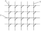
图1为现有技术中的触摸屏的结构示意图,如图1所示,现有技术中的触摸屏为电压感应式触摸屏,所述触摸屏包括:阵列基板和彩膜基板,所述阵列基板包括栅线1、数据线2和一套独立的实现触摸功能的触控扫描线3、触控感应线4和感光单元5,所述感光单元5包括两个独立的感光结构,触控扫描线3和触控感应线4分别连接一个感光结构。当触摸屏被触摸时,感光结构会分别向对应的触控扫描线3或触控感应线4发送一个电信号。触摸屏的控制单元接收到触控扫描线3和触控感应线4返回的电信号后可以计算出触控点的坐标,从而现实对触摸点的定位。Fig. 1 is a schematic structural diagram of a touch screen in the prior art. As shown in Fig. 1, the touch screen in the prior art is a voltage-sensitive touch screen, and the touch screen includes: an array substrate and a color filter substrate, and the array substrate includes
触摸屏在显示时,光线经由背光板发射出来,但是并非所有的光线都能穿过面板,比如信号走线(数据线1、栅线2、触控扫描线3、触控感应线4)、薄膜场效应晶体管(Thin Film Transistor,简称TFT)和储存电容等地方。这些地方除了不完全透光外,而且经过这些地方的光线不受电压控制,从而无法显示正确的灰阶,所以这些地方都需利用黑矩阵加以遮蔽,以免干扰其它透光区域。When the touch screen is displayed, the light is emitted through the backlight panel, but not all the light can pass through the panel, such as signal wiring (
现有技术将触控扫描线3和触控感应线4都设置在已经形成有栅线和数据线的阵列基板上,使得彩膜基板上的黑矩阵的面积必然要增大,使得像素单元的透光区域减小,从而使得像素单元的开口率下降。In the prior art, both the
将触控扫描线3和触控感应线4设置在阵列基板上,还会使得阵列基板上的走线过多,而增加制备触摸屏的工艺难度,相应的工艺不良也会增多。Arranging the
发明内容Contents of the invention
本发明提供了一种彩膜基板及其制造方法、触摸屏和显示装置,本发明能提高像素的开口率,降低触摸屏的工艺难度,提升了工艺良率。The invention provides a color filter substrate and a manufacturing method thereof, a touch screen and a display device. The invention can increase the aperture ratio of pixels, reduce the process difficulty of the touch screen, and improve the process yield.
为实现上述目的,本发明提供一种彩膜基板,包括:衬底基板和位于所述衬底基板上的黑矩阵,所述黑矩阵限定出若干个像素单元,每个所述像素单元内设置有彩膜,该彩膜基板还包括:感光单元、相互绝缘的触控扫描线和触控感应线,所述感光单元位于所述像素单元内,所述感光单元、所述触控扫描线和所述触控感应线设置于所述黑矩阵所对应的区域内,所述感光单元与所述触控扫描线和所述触控感应线接触。In order to achieve the above object, the present invention provides a color filter substrate, including: a base substrate and a black matrix located on the base substrate, the black matrix defines several pixel units, and each of the pixel units is set There is a color film, and the color film substrate also includes: a photosensitive unit, a touch scanning line and a touch sensing line insulated from each other, the photosensitive unit is located in the pixel unit, and the photosensitive unit, the touch scanning line and the The touch sensing line is disposed in the area corresponding to the black matrix, and the photosensitive unit is in contact with the touch scanning line and the touch sensing line.
可选地,所述感光单元为一体化结构,所述感光单元当被特定的光线照射时导通所述触控扫描线和所述触控感应线。Optionally, the photosensitive unit is an integrated structure, and the photosensitive unit conducts the touch scanning line and the touch sensing line when irradiated by a specific light.
可选地,所述触控扫描线上施加时序脉冲信号;所述触控感应线在感光单元导通时输出与所述触控扫描线上时序相同的脉冲信号。Optionally, a timing pulse signal is applied to the touch scanning line; the touch sensing line outputs a pulse signal with the same timing as that on the touch scanning line when the photosensitive unit is turned on.
可选地,在每个所述像素单元内都设置有所述感光单元,或在间隔的所述像素单元内设置有所述感光单元。Optionally, the photosensitive unit is provided in each of the pixel units, or the photosensitive unit is provided in alternate pixel units.
可选地,所述感光单元为光敏半导体。Optionally, the photosensitive unit is a photosensitive semiconductor.
为实现上述目的,本发明还提供一种触摸屏,包括:相对设置的阵列基板和彩膜基板,所述阵列基板包括:栅线和数据线,所述彩膜基板采用上述的彩膜基板。To achieve the above object, the present invention also provides a touch screen, comprising: an array substrate and a color filter substrate oppositely arranged, the array substrate includes: gate lines and data lines, and the color filter substrate adopts the above-mentioned color filter substrate.
可选地,所述触摸屏还包括:信号加载单元和信号处理单元;所述信号加载单元用于向所述触控扫描线加载所述触控扫描信号;Optionally, the touch screen further includes: a signal loading unit and a signal processing unit; the signal loading unit is configured to load the touch scanning signal to the touch scanning line;
所述信号处理单元用于接收并处理所述触控感应线中的所述触控感应信号。The signal processing unit is used for receiving and processing the touch sensing signal in the touch sensing line.
可选地,所述信号加载单元和信号处理单元均设置于所述彩膜基板上,所述信号加载单元与所述触控扫描线连接;所述信号处理单元与所述触控感应线连接。Optionally, both the signal loading unit and the signal processing unit are arranged on the color filter substrate, the signal loading unit is connected to the touch scanning line; the signal processing unit is connected to the touch sensing line .
可选地,所述信号加载单元和信号处理单元均设置于所述阵列基板上,所述信号加载单元通过柔性电路板与所述触控扫描线连接,所述信号处理单元通过柔性电路板与所述触控感应线连接。Optionally, both the signal loading unit and the signal processing unit are arranged on the array substrate, the signal loading unit is connected to the touch scanning line through a flexible circuit board, and the signal processing unit is connected to the touch scanning line through a flexible circuit board. The touch sensing line is connected.
为实现上述目的,本发明还提供一种彩膜基板的制造方法,包括:To achieve the above purpose, the present invention also provides a method for manufacturing a color filter substrate, including:
在衬底基板上形成触控扫描线。A touch scanning line is formed on the base substrate.
在所述衬底基板上形成触控感应线,触控扫描线和触控感应线相互绝缘。A touch sensing line is formed on the base substrate, and the touch scanning line and the touch sensing line are insulated from each other.
在所述衬底基板上形成感光单元,所述感光单元与所述触控扫描线和所述触控感应线接触。A photosensitive unit is formed on the base substrate, and the photosensitive unit is in contact with the touch scanning line and the touch sensing line.
在所述衬底基板上形成黑矩阵和彩膜,所述黑矩阵限定出若干个像素单元,每个所述像素单元内设置有彩膜,所述感光单元位于所述像素单元内,所述感光单元、所述触控扫描线和所述触控感应线设置于所述黑矩阵所对应的区域内。A black matrix and a color filter are formed on the base substrate, the black matrix defines several pixel units, each pixel unit is provided with a color filter, the photosensitive unit is located in the pixel unit, the The photosensitive unit, the touch scanning line and the touch sensing line are arranged in the corresponding area of the black matrix.
本发明具有以下有益效果:The present invention has the following beneficial effects:
本发明提供一种彩膜基板及其制造方法和触摸屏,通过将实现触摸功能的感光单元、触控扫描线和触控感应线设置在彩膜基板上,可有效提高像素单元的开口率,同时也降低了触摸屏的工艺难度,提升了工艺良率。The invention provides a color filter substrate, a manufacturing method thereof, and a touch screen. By arranging a photosensitive unit, a touch scanning line, and a touch sensing line for realizing a touch function on the color filter substrate, the aperture ratio of a pixel unit can be effectively improved, and at the same time It also reduces the process difficulty of the touch screen and improves the process yield.
附图说明Description of drawings
图1为现有技术中的触摸屏的结构示意图;FIG. 1 is a schematic structural view of a touch screen in the prior art;
图2为本发明实施例一提供的彩膜基板的示意图;FIG. 2 is a schematic diagram of a color filter substrate provided in
图3为本发明实施例一提供的彩膜基板上的等效电路图;FIG. 3 is an equivalent circuit diagram on the color filter substrate provided by
图4为触控扫描线施加信号的时序图;FIG. 4 is a timing diagram of signals applied to touch scanning lines;
图5为本发明实施例二提供的触摸屏上的等效电路图;FIG. 5 is an equivalent circuit diagram on the touch screen provided by
图6为本发明实施例二提供的触摸屏中的阵列基板的示意图;FIG. 6 is a schematic diagram of an array substrate in a touch screen provided by
图7为本发明实施例三提供的彩膜基板的制造方法的流程图。FIG. 7 is a flowchart of a method for manufacturing a color filter substrate according to
具体实施方式Detailed ways
为使本领域的技术人员更好地理解本发明的技术方案,下面结合附图对本发明提供的彩膜基板及其制造方法和触摸屏进行详细描述。In order for those skilled in the art to better understand the technical solution of the present invention, the color filter substrate provided by the present invention, its manufacturing method, and the touch screen will be described in detail below with reference to the accompanying drawings.
实施例一Embodiment one
图2为本发明实施例一提供的彩膜基板的示意图,如图2所示,该彩膜基板包括:衬底基板和位于衬底基板上的黑矩阵,黑矩阵限定出若干个像素单元,每个像素单元内设置有彩膜,彩膜基板还包括:感光单元5、触控扫描线3和触控感应线4,感光单元5位于像素单元内,感光单元5、触控扫描线3和触控感应线4设置于与黑矩阵对应的区域内,感光单元5与触控扫描线3和触控感应线4接触。其中,感光单元5、触控扫描线3和触控感应线4设置于与黑矩阵对应的区域内具体指:触控扫描线3和触控感应线4可以位于黑矩阵的下方或者上方,或者部分位于上方,另一部分位于下方,例如,触控扫描线位于黑矩阵的下方,触控感应线位于黑矩阵的上方,黑矩阵可以遮蔽触控扫描线3和触控感应线4,但感光单元5必须位于黑矩阵远离阵列基板的一侧,或者说必须使感光单元5位于能够接收外界光线的一侧。如果触摸感应线和/或触摸扫描线与感光单元不在黑矩阵的同一侧,可通过过孔或其他方式将触摸感应线和/或触摸扫描线与感光单元连接。在图2中,衬底基板、黑矩阵均未示出。Fig. 2 is a schematic diagram of a color filter substrate provided in
其中,每个像素单元内的彩膜层可以包括红、绿、蓝三色彩膜,也可以包括红、绿、蓝、白四色彩膜区域,还可以包括红、绿、蓝、黄四色彩膜区域或者其他能够实现正常显示的多个彩膜区域。本实施例以包括红、绿、蓝三色彩膜区域为例进行说明。Wherein, the color film layer in each pixel unit may include red, green, and blue three-color films, may also include red, green, blue, and white four-color film areas, and may also include red, green, blue, and yellow four-color films. area or other multiple color filter areas that can achieve normal display. In this embodiment, the region including the red, green and blue color filters is taken as an example for illustration.
本方案中,感光单元5具体可以设置在红色彩膜区域内,也可以设置在绿色彩膜区域内,或者设置在蓝色彩膜区域内,优选设置在蓝色彩膜区域内,由于人眼对蓝色的敏感度比较低,这样设置,可以使人眼不太容易察觉到由于设置感光单元5而导致的显示效果的差异,保证较好的显示效果。In this solution, the
在本发明的实施一的技术方案中,将实现触控功能的触控扫描线3和触控感应线4设置在彩膜基板上,可减小阵列基板中像素单元内布线的复杂度,降低了阵列基板的工艺难度,提升了工艺良率。In the technical solution of
需要说明的是,本发明中彩膜基板上的黑矩阵的位置与阵列基板上的栅线和数据线的位置相对应。彩膜区域与栅线和数据线在阵列基板上限定的像素单元相对应。It should be noted that the positions of the black matrix on the color filter substrate in the present invention correspond to the positions of the gate lines and data lines on the array substrate. The color filter area corresponds to the pixel unit defined by the gate line and the data line on the array substrate.
下面将结合图2详细的阐述本发明的技术方案的原理,本发明将触控扫描线3和触控感应线4都设置在彩膜基板上,而且触控扫描线3和触控感应线4都设置在黑矩阵的下方或者黑矩阵的上方或者其中之一设置在黑矩阵的上方,另一个设置在黑矩阵的下方,使得彩膜基板上的触控扫描线3和触控感应线4的位置与阵列基板上的栅线和数据线的位置对应,因而,原本只能遮蔽栅线和数据线的黑矩阵即使不增大面积也能实现对触控扫描线3和触控感应线4的遮蔽,因此像素单元的透光区域也不会减小,所以相较现有技术本发明有效提高了像素单元的开口率。The principle of the technical solution of the present invention will be described in detail below in conjunction with FIG. 2. In the present invention, both the
较优地,感光单元5为一体化结构,感光单元5当被特定的光线照射时导通触控扫描线3和触控感应线4。进一步地,触控扫描线3上施加时序脉冲信号;触控感应线4在感光单元5导通时输出与触控扫描线3上时序相同的脉冲信号。本发明实施例一提供的彩膜基板在进行触控定位时可采用逐行扫描的工作方式。Preferably, the
图3为本发明实施例一提供的彩膜基板上的等效电路图,图4为触控扫描线施加信号的时序图,如图3和图4所示,外部的控制单元接收到开始触控信号的同时外部控制单元向触控扫描线施加信号,该信号为时序脉冲信号。触控扫描线3逐行的接收到脉冲信号,即第一行触控扫描线接收到第一个脉冲信号的下降沿对应第二行触控扫描线接收到的第一个脉冲信号的上升沿,第二行触控扫描线的接收到的第一个脉冲信号的下降沿对应第三行触控扫描线接收到的第一个脉冲信号的上升沿,如此顺序扫描,直到完成所有触控扫描线3的扫描,再从第一行开始重复上述过程。Fig. 3 is an equivalent circuit diagram on the color filter substrate provided by
在进行逐行扫描的过程中,如没有触摸动作,由于感光单元5的导电性能很差,因此,触控感应线4会输出一个低电平信号或者没有信号输出;若有触摸动作,使得感光单元5被特定的光线照射,感光单元5将导通触控扫描线3和触控感应线4,触控感应线4输出的信号会发生变化,触控感应线4会输出与触控扫描线5上时序相同的脉冲信号,外部的处理单元接收到触控感应线4输出的脉冲信号并通过判断此脉冲信号来判断触控发生的位置,即X坐标的位置可以通过触控感应线4的位置确定,Y坐标的位置可以通过将触控感应线4中的脉冲信号与每行触控扫描线3中的脉冲信号相对比得到。In the process of performing progressive scanning, if there is no touch action, because the conductivity of the
下面对上述位置确定进行举例说明。假设在第二行第三个像素的位置发生触控动作,将该点坐标定义为(3,2),则第二行触控扫描线与第三列像素对应的触控感应线通过感光单元导通,第三列的触控感应线会输出一个波形与第二行触控扫描线中脉冲信号的波形相同的脉冲信号,但强度可能会略有差别,通过将触控感应线输出的脉冲信号的波形与各条触控扫描线的波形进行对比,可以确定触控位置的Y坐标,X坐标可以通过输出脉冲信号的的触控感应线的位置确定。The above location determination is described below with an example. Assuming that a touch action occurs at the position of the third pixel in the second row, and the coordinates of this point are defined as (3, 2), then the touch scanning line in the second row and the touch sensing line corresponding to the pixel in the third column pass through the photosensitive unit turn on, the touch sensing line in the third column will output a pulse signal with the same waveform as the pulse signal in the touch scanning line in the second row, but the intensity may be slightly different. By comparing the waveform of the signal with the waveform of each touch scanning line, the Y coordinate of the touch position can be determined, and the X coordinate can be determined by the position of the touch sensing line outputting the pulse signal.
当触摸点的位置为多个时,处理单元会接收到多个脉冲信号,但是由于采用这种逐行扫描的方式,使得处理单元在接收到每个脉冲信号的时序是不同的,处理单元可通过时序区别出每个脉冲信号,并通过计算可得出每个脉冲信号所对应的位置,即实现了多点触控功能。When there are multiple touch points, the processing unit will receive multiple pulse signals, but due to the progressive scanning method, the processing unit receives each pulse signal at a different timing, and the processing unit can Each pulse signal is distinguished through timing, and the position corresponding to each pulse signal can be obtained through calculation, that is, the multi-touch function is realized.
本发明实施一中的触控扫描线3的数量为n行,触控感应线4的数量为m列,感光单元5的数量为m×n,则该彩膜基板的触控单元的数量为m×n。在实际设计过程中,触控单元的数量可根据实际情况进行设定。In
感光单元5为采用一体化结构,同时触控模块采用逐行扫描的工作方式,可有效的防止在触摸时“鬼点”的出现。所谓鬼点是在多点触摸屏上出现的,例如,现有技术中的触摸屏有两点触摸时,在屏上位置会出现两个横坐标点、两个纵坐标点,综合起来就是4个点,但实际上只触摸了两个点,另外两个点就是鬼点。The
当然,利用感光单元5、触控扫描线3和触控感应线4对触摸点定位的工作方式还可有多种,上述的将感光单元设计为一体化结构以及利用逐行扫描这种工作方式均为本发明的优选方案,并不构成对本发明的限定。Of course, there are many ways to position the touch point by using the
可选地,在每个像素单元内都设置有感光单元5,或在间隔的像素单元内设置有感光单元5。在每个像素单元内都设置感光单元5可实现对触摸点的精准定位。在实际使用中也可在间隔的像素单元内设置感光单元5,因为像素单元的尺寸较小,而利用手指触摸屏幕时,手指的接触面积一般都会比较大,因此可以不必在每个像素单元内都设置感光单元5。Optionally, a
可选地,感光单元5为光敏半导体。Optionally, the
本发明实施例一提供了一种彩膜基板,将实现触摸功能的感光单元、触控扫描线和触控感应线设置在彩膜基板上。本发明实施例一的技术方案不但能有效提高像素单元的开口率,而且也降低了触摸屏的工艺难度,提升了工艺良率,同时还能实现多点触控功能。
实施例二Embodiment two
本发明实施例二提供了一种触摸屏,该触摸屏包括:相对设置的阵列基板和彩膜基板,阵列基板包括:栅线和数据线,彩膜基板采用上述实施例提供的彩膜基板。
图5为本发明实施例二提供的触摸屏上的等效电路图,如图5所示,可选地,触摸屏包括信号加载单元6和信号处理单元7,信号加载单元6用于向触控扫描线3加载触控扫描信号,信号处理单元7用于接收并处理触控感应线4中的触控感应信号,在触控扫描线3和触控感应线4的交叉处设置有感光单元5,感光单元5分别与一条触控扫描线3和一条触控感应线4接触。本发明实施例二中的信号加载单元6的功能与上述实施例一中的控制单元的功能相同,且触控扫描信号也可为时序脉冲信号,信号处理单元7的功能与上述实施例一中的处理单元的功能相同,且触控感应信号也可为脉冲信号。但是现有技术中将控制单元和处理单元集成在显示屏外部的电路板上,而本发明实施例二的技术方案可将信号加载单元6和信号处理单元7直接设置于阵列基板或彩膜基板上,该技术手段可有效的利用触摸屏的空间。FIG. 5 is an equivalent circuit diagram on the touch screen provided by
可选地,信号加载单元6和信号处理单元7位于彩膜基板上,信号加载单元6与触控扫描线3连接,信号处理单元7与触控感应线4连接。或者,信号加载单元6和信号处理单元7位于阵列基板上,信号加载单元6通过柔性电路板(Flexible Printed Circuit,简称PCB板)与触控扫描线3连接,信号处理单元7通过柔性电路板与触控感应线4连接。Optionally, the signal loading unit 6 and the signal processing unit 7 are located on the color filter substrate, the signal loading unit 6 is connected to the
本发明实施例二提供的触摸屏中的彩膜基板的结构示意图可参照图2,具体的结构特征以及产生的技术效果可参见上述实施例一中,此处不再赘述。本发明实施例二提供的触摸屏中的阵列基板的结构示意图参见图6所示,阵列基板上设置有用于显示功能的栅线1和数据线2,而没有了用于触控功能的触控扫描线和触控感应线。因而可使得像素单元内走线变的简单,触摸屏的工艺难度降低,更重要的是,由于像素单元内的显示区域的面积变大,使得像素单元的开口率得到了提高。Refer to FIG. 2 for a structural schematic diagram of the color filter substrate in the touch screen provided by
需要说明的是,在图6中R、G、B仅代表位于彩膜基板上的红色彩膜R、绿色彩膜G以及蓝色彩膜B对应在阵列基板上的区域,而不是代表彩膜本身。It should be noted that in Figure 6, R, G, and B only represent the areas on the array substrate corresponding to the red color filter R, green color filter G, and blue color filter B on the color filter substrate, rather than the color filter itself. .
本发明实施例二提供了一种触摸屏,将实现触摸功能的感光单元、触控扫描线和触控感应线设置在彩膜基板上。本发明实施例二的技术方案不但能有效提高像素单元的开口率,而且也降低了触摸屏的工艺难度,提升了工艺良率,同时还能实现多点触控功能。
实施例三Embodiment Three
图7为本发明实施例三提供的彩膜基板的制造方法的流程图,如图7所示,该彩膜基板包括:衬底基板、位于衬底基板上的黑矩阵、感光单元、触控扫描线和触控感应线,黑矩阵限定出若干个像素单元,每个像素单元内设置有彩膜,该制造方法包括:Fig. 7 is a flow chart of the manufacturing method of the color filter substrate provided by
步骤101:在衬底基板上形成触控扫描线。Step 101: forming a touch scanning line on a base substrate.
步骤102:在衬底基板上形成触控感应线,触控扫描线和触控感应线相互绝缘。Step 102: Form a touch sensing line on the base substrate, and the touch scanning line and the touch sensing line are insulated from each other.
步骤103:在衬底基板上形成感光单元,感光单元与触控扫描线和触控感应线接触。Step 103: forming a photosensitive unit on the base substrate, the photosensitive unit is in contact with the touch scanning line and the touch sensing line.
步骤104:在衬底基板上形成黑矩阵和彩膜,黑矩阵限定出若干个像素单元,每个像素单元内设置有彩膜,感光单元位于像素单元内,感光单元、触控扫描线和触控感应线设置于黑矩阵所对应的区域内。Step 104: Form a black matrix and a color filter on the base substrate, the black matrix defines several pixel units, each pixel unit is provided with a color filter, the photosensitive unit is located in the pixel unit, the photosensitive unit, the touch scanning line and the touch The control sensing line is arranged in the area corresponding to the black matrix.
需要说明的是步骤101、步骤102、步骤103和步骤104的顺序可任意调换,即对触控扫描线、触控感应线、感光单元、黑矩阵和彩膜的制造顺序没有限制。例如:可以先形成感光单元,再形成触控扫描线、触控感应线,再将感光单元连接触控扫描线和触控感应线,最后再形成黑矩阵和彩膜。但是感光单元必须位于黑矩阵远离阵列基板的一侧,或者说必须使感光单元位于能够接收外界光线的一侧。It should be noted that the order of
本发明实施例三提供了一种彩膜基板的制造方法,先将实现触摸功能的感光单元、触控扫描线和触控感应线设置在彩膜基板上,再在衬底基板上形成黑矩阵和彩膜。本发明实施例四的技术方案不但能有效提高像素单元的开口率,而且也降低了整个触摸屏的工艺难度,提升了工艺良率,同时还能实现多点触控功能。
需要说明的是,本发明中的触控扫描线和触控感应线的材料可以为铝(Al)、钼(Mo)或铜(Cu)铜等金属材料,触控扫描线和触控感应线的材料还可为氧化铟锡(Indium Tin Oxides,简称ITO)。本发明所提供的技术方案可应用于盒内触摸(In-Cell Touch)屏上。It should be noted that the materials of the touch scanning lines and touch sensing lines in the present invention can be metal materials such as aluminum (Al), molybdenum (Mo) or copper (Cu), and the touch scanning lines and touch sensing lines The material can also be indium tin oxide (Indium Tin Oxides, referred to as ITO). The technical solution provided by the invention can be applied to an In-Cell Touch screen.
可以理解的是,以上实施方式仅仅是为了说明本发明的原理而采用的示例性实施方式,然而本发明并不局限于此。对于本领域内的普通技术人员而言,在不脱离本发明的精神和实质的情况下,可以做出各种变型和改进,这些变型和改进也视为本发明的保护范围。It can be understood that, the above embodiments are only exemplary embodiments adopted for illustrating the principle of the present invention, but the present invention is not limited thereto. For those skilled in the art, various modifications and improvements can be made without departing from the spirit and essence of the present invention, and these modifications and improvements are also regarded as the protection scope of the present invention.
Claims (10)
Priority Applications (3)
| Application Number | Priority Date | Filing Date | Title |
|---|---|---|---|
| CN201310302567.XACN103412673B (en) | 2013-07-18 | 2013-07-18 | Colored film substrate, manufacturing method of colored film substrate and touch screen |
| US14/436,916US9778793B2 (en) | 2013-07-18 | 2013-11-01 | Color filter substrate to be disposed opposite to an array substrate and manufacturing method thereof |
| PCT/CN2013/086421WO2015007030A1 (en) | 2013-07-18 | 2013-11-01 | Colour film substrate and manufacturing method therefor, and touchscreen |
Applications Claiming Priority (1)
| Application Number | Priority Date | Filing Date | Title |
|---|---|---|---|
| CN201310302567.XACN103412673B (en) | 2013-07-18 | 2013-07-18 | Colored film substrate, manufacturing method of colored film substrate and touch screen |
Publications (2)
| Publication Number | Publication Date |
|---|---|
| CN103412673Atrue CN103412673A (en) | 2013-11-27 |
| CN103412673B CN103412673B (en) | 2017-02-15 |
Family
ID=49605689
Family Applications (1)
| Application Number | Title | Priority Date | Filing Date |
|---|---|---|---|
| CN201310302567.XAExpired - Fee RelatedCN103412673B (en) | 2013-07-18 | 2013-07-18 | Colored film substrate, manufacturing method of colored film substrate and touch screen |
Country Status (3)
| Country | Link |
|---|---|
| US (1) | US9778793B2 (en) |
| CN (1) | CN103412673B (en) |
| WO (1) | WO2015007030A1 (en) |
Cited By (7)
| Publication number | Priority date | Publication date | Assignee | Title |
|---|---|---|---|---|
| CN104698522A (en)* | 2015-03-26 | 2015-06-10 | 南京中电熊猫液晶显示科技有限公司 | Touch type colored light filter and manufacturing method thereof, touch display panel |
| CN104750320A (en)* | 2015-04-22 | 2015-07-01 | 京东方科技集团股份有限公司 | Infrared touch module, infrared touch device and touch position determining method |
| WO2015096214A1 (en)* | 2013-12-26 | 2015-07-02 | 深圳市华星光电技术有限公司 | In-cell touch control array substrate and liquid crystal display (lcd) panel |
| CN106990876A (en)* | 2016-03-08 | 2017-07-28 | 罗天成 | It is a kind of to carry touch function electronic product without the new of additional touch-screen |
| EP3203358A4 (en)* | 2014-09-29 | 2018-05-23 | Boe Technology Group Co. Ltd. | Touch control display panel and display device |
| CN108107633A (en)* | 2017-11-20 | 2018-06-01 | 友达光电股份有限公司 | Pixel structure and curved surface display device |
| WO2019237660A1 (en)* | 2018-06-12 | 2019-12-19 | 广州视源电子科技股份有限公司 | Direct type backlight display module and display device |
Families Citing this family (3)
| Publication number | Priority date | Publication date | Assignee | Title |
|---|---|---|---|---|
| CN103280448B (en)* | 2013-04-27 | 2016-01-06 | 北京京东方光电科技有限公司 | A kind of array base palte and preparation method thereof, display unit |
| US10684500B2 (en) | 2015-05-27 | 2020-06-16 | Semiconductor Energy Laboratory Co., Ltd. | Touch panel |
| CN106653770A (en)* | 2016-12-27 | 2017-05-10 | 武汉华星光电技术有限公司 | Display panel and array substrate thereof |
Citations (6)
| Publication number | Priority date | Publication date | Assignee | Title |
|---|---|---|---|---|
| US20100214247A1 (en)* | 2009-02-20 | 2010-08-26 | Acrosense Technology Co., Ltd. | Capacitive Touch Panel |
| CN101825787A (en)* | 2009-03-04 | 2010-09-08 | 北京京东方光电科技有限公司 | Touch display screen and manufacture method thereof |
| CN202351848U (en)* | 2011-11-18 | 2012-07-25 | 京东方科技集团股份有限公司 | Touch liquid crystal display |
| CN102929031A (en)* | 2012-10-31 | 2013-02-13 | 北京京东方光电科技有限公司 | Color membrane substrate and manufacture method thereof and touch display device and driving method thereof |
| CN103019448A (en)* | 2012-12-21 | 2013-04-03 | 北京京东方光电科技有限公司 | Manufacture method of color film substrate, color film substrate and display device |
| CN203376707U (en)* | 2013-07-18 | 2014-01-01 | 合肥京东方光电科技有限公司 | Color film substrate, touch screen and touch device |
Family Cites Families (13)
| Publication number | Priority date | Publication date | Assignee | Title |
|---|---|---|---|---|
| US20050243023A1 (en)* | 2004-04-06 | 2005-11-03 | Damoder Reddy | Color filter integrated with sensor array for flat panel display |
| US7495713B2 (en)* | 2006-08-07 | 2009-02-24 | Hannstar Display Corp. | Touch panel |
| US7960682B2 (en)* | 2007-12-13 | 2011-06-14 | Apple Inc. | Display device control based on integrated ambient light detection and lighting source characteristics |
| TWI380089B (en)* | 2008-12-03 | 2012-12-21 | Au Optronics Corp | Method of forming a color filter touch sensing substrate |
| US8692808B2 (en)* | 2009-06-16 | 2014-04-08 | Au Optronics Corp. | Touch panel |
| JP2012230132A (en)* | 2009-09-09 | 2012-11-22 | Sharp Corp | Optical sensor and display device |
| CN101751188B (en)* | 2010-01-27 | 2012-04-25 | 汕头超声显示器(二厂)有限公司 | Display device of built-in sensitive device |
| TWI471796B (en)* | 2011-02-11 | 2015-02-01 | Wintek Corp | Touch-sensitive display device |
| KR101878976B1 (en)* | 2011-07-07 | 2018-07-17 | 삼성디스플레이 주식회사 | Method of driving touch sensing display panel and display apparatus performing the same |
| US9470941B2 (en)* | 2011-08-19 | 2016-10-18 | Apple Inc. | In-cell or on-cell touch sensor with color filter on array |
| CN102955622B (en)* | 2012-10-19 | 2016-04-13 | 京东方科技集团股份有限公司 | Based on the optical sensing formula touch-screen and preparation method thereof of multi-dimensional electric field mode |
| CN103049156B (en)* | 2012-12-13 | 2015-12-23 | 北京京东方光电科技有限公司 | A kind of capacitance type in-cell touch panel and display device |
| WO2016144108A1 (en)* | 2015-03-10 | 2016-09-15 | 크루셜텍 (주) | Display device capable of scanning images |
- 2013
- 2013-07-18CNCN201310302567.XApatent/CN103412673B/ennot_activeExpired - Fee Related
- 2013-11-01USUS14/436,916patent/US9778793B2/enactiveActive
- 2013-11-01WOPCT/CN2013/086421patent/WO2015007030A1/enactiveApplication Filing
Patent Citations (6)
| Publication number | Priority date | Publication date | Assignee | Title |
|---|---|---|---|---|
| US20100214247A1 (en)* | 2009-02-20 | 2010-08-26 | Acrosense Technology Co., Ltd. | Capacitive Touch Panel |
| CN101825787A (en)* | 2009-03-04 | 2010-09-08 | 北京京东方光电科技有限公司 | Touch display screen and manufacture method thereof |
| CN202351848U (en)* | 2011-11-18 | 2012-07-25 | 京东方科技集团股份有限公司 | Touch liquid crystal display |
| CN102929031A (en)* | 2012-10-31 | 2013-02-13 | 北京京东方光电科技有限公司 | Color membrane substrate and manufacture method thereof and touch display device and driving method thereof |
| CN103019448A (en)* | 2012-12-21 | 2013-04-03 | 北京京东方光电科技有限公司 | Manufacture method of color film substrate, color film substrate and display device |
| CN203376707U (en)* | 2013-07-18 | 2014-01-01 | 合肥京东方光电科技有限公司 | Color film substrate, touch screen and touch device |
Cited By (10)
| Publication number | Priority date | Publication date | Assignee | Title |
|---|---|---|---|---|
| WO2015096214A1 (en)* | 2013-12-26 | 2015-07-02 | 深圳市华星光电技术有限公司 | In-cell touch control array substrate and liquid crystal display (lcd) panel |
| EP3203358A4 (en)* | 2014-09-29 | 2018-05-23 | Boe Technology Group Co. Ltd. | Touch control display panel and display device |
| US10254898B2 (en) | 2014-09-29 | 2019-04-09 | Boe Technology Group Co., Ltd. | Touch display panel and display device |
| CN104698522A (en)* | 2015-03-26 | 2015-06-10 | 南京中电熊猫液晶显示科技有限公司 | Touch type colored light filter and manufacturing method thereof, touch display panel |
| CN104750320A (en)* | 2015-04-22 | 2015-07-01 | 京东方科技集团股份有限公司 | Infrared touch module, infrared touch device and touch position determining method |
| CN104750320B (en)* | 2015-04-22 | 2018-04-27 | 京东方科技集团股份有限公司 | The definite method of infrared type touch module, infrared type touching device and touch location |
| CN106990876A (en)* | 2016-03-08 | 2017-07-28 | 罗天成 | It is a kind of to carry touch function electronic product without the new of additional touch-screen |
| CN108107633A (en)* | 2017-11-20 | 2018-06-01 | 友达光电股份有限公司 | Pixel structure and curved surface display device |
| CN108107633B (en)* | 2017-11-20 | 2020-10-30 | 友达光电股份有限公司 | Pixel structure and curved surface display device |
| WO2019237660A1 (en)* | 2018-06-12 | 2019-12-19 | 广州视源电子科技股份有限公司 | Direct type backlight display module and display device |
Also Published As
| Publication number | Publication date |
|---|---|
| US9778793B2 (en) | 2017-10-03 |
| CN103412673B (en) | 2017-02-15 |
| US20150234538A1 (en) | 2015-08-20 |
| WO2015007030A1 (en) | 2015-01-22 |
Similar Documents
| Publication | Publication Date | Title |
|---|---|---|
| CN103412673B (en) | Colored film substrate, manufacturing method of colored film substrate and touch screen | |
| CN104020912B (en) | Capacitive touch structure, embedded touch screen, display device and scanning method of display device | |
| CN103970392B (en) | A kind of touch screen and display device | |
| CN103926729B (en) | Array substrate, color film substrate, touch display device and driving method thereof | |
| CN104022127B (en) | A kind of array base palte and preparation method thereof and display device | |
| CN104020906B (en) | A kind of In-cell touch panel and display device | |
| JP6430536B2 (en) | In-cell touch panel and display device | |
| CN103838431B (en) | A kind of In-cell touch panel and display device | |
| CN106897696B (en) | Grain identification module, driving method thereof and display device | |
| CN104022128B (en) | Array substrate, manufacturing method thereof and displaying device | |
| CN102866815B (en) | Capacitance type embedded touch screen and display device | |
| CN102541335B (en) | Touch display device | |
| CN104020913A (en) | Embedded touch screen and display device | |
| US9830028B2 (en) | In-cell touch panel with self-capacitive electrodes and display device | |
| CN104049800B (en) | Embedded touch screen and display device | |
| CN104536619B (en) | Touch substrate and preparation method thereof, display device | |
| CN101937293A (en) | Information input device and display device | |
| CN104570446B (en) | A kind of touch-control display panel and its control method | |
| CN104915081A (en) | Array substrate, manufacturing method thereof and touch display panel | |
| US20160370913A1 (en) | Display apparatus, electronic apparatus and driving method | |
| CN105739768A (en) | Touch display panel and touch display equipment | |
| CN203376707U (en) | Color film substrate, touch screen and touch device | |
| CN202736016U (en) | Capacitive embedded touch screen and display device | |
| TWI480781B (en) | Touch screen device | |
| CN104035639B (en) | Capacitance touch structure, In-cell touch panel, display device and scan method thereof |
Legal Events
| Date | Code | Title | Description |
|---|---|---|---|
| C06 | Publication | ||
| PB01 | Publication | ||
| C10 | Entry into substantive examination | ||
| SE01 | Entry into force of request for substantive examination | ||
| C14 | Grant of patent or utility model | ||
| GR01 | Patent grant | ||
| CF01 | Termination of patent right due to non-payment of annual fee | Granted publication date:20170215 Termination date:20210718 | |
| CF01 | Termination of patent right due to non-payment of annual fee |