CN103412450A - Array substrate, manufacturing method thereof and display device - Google Patents
Array substrate, manufacturing method thereof and display deviceDownload PDFInfo
- Publication number
- CN103412450A CN103412450ACN2013103198024ACN201310319802ACN103412450ACN 103412450 ACN103412450 ACN 103412450ACN 2013103198024 ACN2013103198024 ACN 2013103198024ACN 201310319802 ACN201310319802 ACN 201310319802ACN 103412450 ACN103412450 ACN 103412450A
- Authority
- CN
- China
- Prior art keywords
- layer
- oxide semiconductor
- metal oxide
- semiconductor layer
- mobility
- Prior art date
- Legal status (The legal status is an assumption and is not a legal conclusion. Google has not performed a legal analysis and makes no representation as to the accuracy of the status listed.)
- Pending
Links
Images


Classifications
- H—ELECTRICITY
- H10—SEMICONDUCTOR DEVICES; ELECTRIC SOLID-STATE DEVICES NOT OTHERWISE PROVIDED FOR
- H10D—INORGANIC ELECTRIC SEMICONDUCTOR DEVICES
- H10D30/00—Field-effect transistors [FET]
- H10D30/60—Insulated-gate field-effect transistors [IGFET]
- H10D30/67—Thin-film transistors [TFT]
- H10D30/674—Thin-film transistors [TFT] characterised by the active materials
- H10D30/6755—Oxide semiconductors, e.g. zinc oxide, copper aluminium oxide or cadmium stannate
- H—ELECTRICITY
- H10—SEMICONDUCTOR DEVICES; ELECTRIC SOLID-STATE DEVICES NOT OTHERWISE PROVIDED FOR
- H10D—INORGANIC ELECTRIC SEMICONDUCTOR DEVICES
- H10D30/00—Field-effect transistors [FET]
- H10D30/60—Insulated-gate field-effect transistors [IGFET]
- H10D30/67—Thin-film transistors [TFT]
- H10D30/6757—Thin-film transistors [TFT] characterised by the structure of the channel, e.g. transverse or longitudinal shape or doping profile
- H—ELECTRICITY
- H10—SEMICONDUCTOR DEVICES; ELECTRIC SOLID-STATE DEVICES NOT OTHERWISE PROVIDED FOR
- H10D—INORGANIC ELECTRIC SEMICONDUCTOR DEVICES
- H10D86/00—Integrated devices formed in or on insulating or conducting substrates, e.g. formed in silicon-on-insulator [SOI] substrates or on stainless steel or glass substrates
- H10D86/01—Manufacture or treatment
- H10D86/021—Manufacture or treatment of multiple TFTs
- H10D86/0221—Manufacture or treatment of multiple TFTs comprising manufacture, treatment or patterning of TFT semiconductor bodies
- H—ELECTRICITY
- H10—SEMICONDUCTOR DEVICES; ELECTRIC SOLID-STATE DEVICES NOT OTHERWISE PROVIDED FOR
- H10D—INORGANIC ELECTRIC SEMICONDUCTOR DEVICES
- H10D86/00—Integrated devices formed in or on insulating or conducting substrates, e.g. formed in silicon-on-insulator [SOI] substrates or on stainless steel or glass substrates
- H10D86/01—Manufacture or treatment
- H10D86/021—Manufacture or treatment of multiple TFTs
- H10D86/0231—Manufacture or treatment of multiple TFTs using masks, e.g. half-tone masks
- H—ELECTRICITY
- H10—SEMICONDUCTOR DEVICES; ELECTRIC SOLID-STATE DEVICES NOT OTHERWISE PROVIDED FOR
- H10D—INORGANIC ELECTRIC SEMICONDUCTOR DEVICES
- H10D86/00—Integrated devices formed in or on insulating or conducting substrates, e.g. formed in silicon-on-insulator [SOI] substrates or on stainless steel or glass substrates
- H10D86/40—Integrated devices formed in or on insulating or conducting substrates, e.g. formed in silicon-on-insulator [SOI] substrates or on stainless steel or glass substrates characterised by multiple TFTs
- H10D86/421—Integrated devices formed in or on insulating or conducting substrates, e.g. formed in silicon-on-insulator [SOI] substrates or on stainless steel or glass substrates characterised by multiple TFTs having a particular composition, shape or crystalline structure of the active layer
- H10D86/423—Integrated devices formed in or on insulating or conducting substrates, e.g. formed in silicon-on-insulator [SOI] substrates or on stainless steel or glass substrates characterised by multiple TFTs having a particular composition, shape or crystalline structure of the active layer comprising semiconductor materials not belonging to the Group IV, e.g. InGaZnO
- H—ELECTRICITY
- H10—SEMICONDUCTOR DEVICES; ELECTRIC SOLID-STATE DEVICES NOT OTHERWISE PROVIDED FOR
- H10D—INORGANIC ELECTRIC SEMICONDUCTOR DEVICES
- H10D86/00—Integrated devices formed in or on insulating or conducting substrates, e.g. formed in silicon-on-insulator [SOI] substrates or on stainless steel or glass substrates
- H10D86/40—Integrated devices formed in or on insulating or conducting substrates, e.g. formed in silicon-on-insulator [SOI] substrates or on stainless steel or glass substrates characterised by multiple TFTs
- H10D86/60—Integrated devices formed in or on insulating or conducting substrates, e.g. formed in silicon-on-insulator [SOI] substrates or on stainless steel or glass substrates characterised by multiple TFTs wherein the TFTs are in active matrices
- H—ELECTRICITY
- H10—SEMICONDUCTOR DEVICES; ELECTRIC SOLID-STATE DEVICES NOT OTHERWISE PROVIDED FOR
- H10D—INORGANIC ELECTRIC SEMICONDUCTOR DEVICES
- H10D99/00—Subject matter not provided for in other groups of this subclass
Landscapes
- Thin Film Transistor (AREA)
Abstract
Translated fromChinese
Description
Translated fromChinese技术领域technical field
本发明涉及显示技术领域,特别涉及一种阵列基板及其制作方法和显示装置。The present invention relates to the field of display technology, in particular to an array substrate, a manufacturing method thereof, and a display device.
背景技术Background technique
随着科技的不断进步,用户对液晶显示设备的需求日益增加,TFT-LCD(Thin Film Transistor-Liquid Crystal Display,薄膜场效应晶体管液晶显示器)也成为了手机、平板电脑等产品中使用的主流显示器。此外,随着显示设备的普及,用户对大尺寸显示产品的需求也越来越普遍。With the continuous advancement of technology, users' demand for liquid crystal display equipment is increasing, and TFT-LCD (Thin Film Transistor-Liquid Crystal Display, Thin Film Field Effect Transistor Liquid Crystal Display) has also become the mainstream display used in mobile phones, tablet computers and other products . In addition, with the popularization of display devices, users' demand for large-size display products is becoming more and more common.
TFT的性能决定了液晶显示器的显示品质。量产中常常采用非晶硅作为有源层,但非晶硅具有较多的缺陷,并且迁移率较低。非晶硅TFT的载流子实际迁移率大致在10cm2/(V*s)左右,但由于缺陷数目太多,栅电极所吸引的大部分电荷被攫取在缺陷中而无法提供导电能力,使得等效载流子迁移率仅仅剩下不到1cm2/(V*s),不能满足大尺寸显示产品的需求。The performance of TFT determines the display quality of LCD. Amorphous silicon is often used as the active layer in mass production, but amorphous silicon has many defects and low mobility. The actual carrier mobility of amorphous silicon TFT is about 10cm2 /(V*s), but due to the large number of defects, most of the charges attracted by the gate electrode are captured in the defects and cannot provide conductivity, making The equivalent carrier mobility is only less than 1cm2 /(V*s), which cannot meet the needs of large-scale display products.
为了提高有源层的迁移率,现有技术采用金属氧化物半导体制作有源层,但有的金属氧化物半导体的迁移率不够高,而有的金属氧化物半导体虽然迁移率比较高,但是漏电流比较大,将会影响TFT的性能,导致显示器不能正常显示。In order to improve the mobility of the active layer, the existing technology uses metal oxide semiconductors to make the active layer, but the mobility of some metal oxide semiconductors is not high enough, and some metal oxide semiconductors have relatively high mobility, but the drain If the current is relatively large, it will affect the performance of the TFT and cause the display to not display normally.
发明内容Contents of the invention
本发明要解决的技术问题是提供一种阵列基板及其制作方法和显示装置,能够制备性能良好、稳定且具有高迁移率的有源层。The technical problem to be solved by the present invention is to provide an array substrate and its manufacturing method and a display device, which can prepare an active layer with good performance, stability and high mobility.
为解决上述技术问题,本发明的实施例提供技术方案如下:In order to solve the above technical problems, embodiments of the present invention provide technical solutions as follows:
一方面,提供一种阵列基板,所述阵列基板的有源层由至少两个金属氧化物半导体层组成,其中,靠近栅绝缘层的第一金属氧化物半导体层的迁移率大于靠近源漏金属层的第二金属氧化物半导体层的迁移率。In one aspect, an array substrate is provided, the active layer of the array substrate is composed of at least two metal oxide semiconductor layers, wherein the mobility of the first metal oxide semiconductor layer close to the gate insulating layer is higher than that close to the source-drain metal layer. The mobility of the second metal oxide semiconductor layer.
进一步地,上述方案中,所述第一金属氧化物半导体层的迁移率大于30cm2/V*s,所述第二金属氧化物半导体层的迁移率为8-10cm2/V*s。Further, in the above solution, the mobility of the first metal oxide semiconductor layer is greater than 30 cm2 /V*s, and the mobility of the second metal oxide semiconductor layer is 8-10 cm2 /V*s.
进一步地,上述方案中,所述第一金属氧化物半导体层的厚度为10nm-50nm,所述第二金属氧化物半导体层的厚度为10nm-50nm。Further, in the above solution, the thickness of the first metal oxide semiconductor layer is 10 nm-50 nm, and the thickness of the second metal oxide semiconductor layer is 10 nm-50 nm.
进一步地,上述方案中,所述第一金属氧化物半导体层为ITZO,所述第二金属氧化物半导体层为IGZO。Further, in the above solution, the first metal oxide semiconductor layer is ITZO, and the second metal oxide semiconductor layer is IGZO.
进一步地,上述方案中,所述阵列基板具体包括:Further, in the above solution, the array substrate specifically includes:
衬底基板;Substrate substrate;
所述衬底基板上的栅电极和栅线;a gate electrode and a gate line on the base substrate;
所述栅电极和所述栅线上的所述栅绝缘层;the gate electrode and the gate insulating layer on the gate line;
所述栅绝缘层上的所述有源层,所述有源层由第一金属氧化物半导体层和第二金属氧化物半导体层组成;the active layer on the gate insulating layer, the active layer is composed of a first metal oxide semiconductor layer and a second metal oxide semiconductor layer;
所述有源层上的刻蚀阻挡层;an etch stop layer on the active layer;
所述刻蚀阻挡层上的由所述源漏金属层组成的漏电极、源电极和数据线;A drain electrode, a source electrode and a data line composed of the source-drain metal layer on the etching barrier layer;
所述漏电极、所述源电极和所述数据线上的钝化层,所述钝化层包括有对应所述漏电极的过孔;The passivation layer on the drain electrode, the source electrode and the data line, the passivation layer includes a via hole corresponding to the drain electrode;
所述钝化层上的像素电极,所述像素电极通过所述过孔与所述漏电极电连接。The pixel electrode on the passivation layer is electrically connected to the drain electrode through the via hole.
本发明实施例还提供了一种显示装置,包括如上所述的阵列基板。An embodiment of the present invention also provides a display device, including the above-mentioned array substrate.
本发明实施例还提供了一种阵列基板的制作方法,利用至少两个金属氧化物半导体层完成有源层的制作,其中,靠近栅绝缘层的第一金属氧化物半导体层的迁移率大于靠近源漏金属层的第二金属氧化物半导体层的迁移率。An embodiment of the present invention also provides a method for fabricating an array substrate. At least two metal oxide semiconductor layers are used to complete the fabrication of the active layer, wherein the mobility of the first metal oxide semiconductor layer close to the gate insulating layer is greater than that close to the gate insulating layer. The mobility of the second metal oxide semiconductor layer of the source-drain metal layer.
进一步地,上述方案中,所述制作方法具体包括:Further, in the above solution, the production method specifically includes:
在衬底基板上依次形成栅金属层和栅绝缘层,所述栅金属层包括栅电极和栅线的图形;sequentially forming a gate metal layer and a gate insulating layer on the base substrate, the gate metal layer including patterns of gate electrodes and gate lines;
在形成有所述栅绝缘层的衬底基板上形成有源层的图形,所述有源层由第一金属氧化物半导体层和第二金属氧化物半导体层组成;forming a pattern of an active layer on the substrate on which the gate insulating layer is formed, the active layer consisting of a first metal oxide semiconductor layer and a second metal oxide semiconductor layer;
在形成有所述有源层的衬底基板上形成刻蚀阻挡层的图形;forming a pattern of an etching stopper layer on the base substrate on which the active layer is formed;
在形成有所述刻蚀阻挡层的衬底基板上形成数据线、源电极和漏电极的图形;forming patterns of data lines, source electrodes, and drain electrodes on the base substrate on which the etching stopper layer is formed;
在形成有所述数据线、所述源电极和所述漏电极的衬底基板上形成钝化层的图形,所述钝化层的图形包括有对应所述漏电极的过孔;forming a pattern of a passivation layer on the base substrate on which the data line, the source electrode, and the drain electrode are formed, and the pattern of the passivation layer includes a via hole corresponding to the drain electrode;
在形成有所述钝化层的衬底基板上形成像素电极的图形,所述像素电极通过所述过孔与所述漏电极电连接。A pattern of a pixel electrode is formed on the base substrate on which the passivation layer is formed, and the pixel electrode is electrically connected to the drain electrode through the via hole.
进一步地,上述方案中,所述在形成有所述栅绝缘层的衬底基板上形成有源层的图形包括:Further, in the above solution, the pattern of forming the active layer on the base substrate on which the gate insulating layer is formed includes:
在形成有所述栅绝缘层的衬底基板上沉积所述第一金属氧化物半导体层;depositing the first metal oxide semiconductor layer on the substrate on which the gate insulating layer is formed;
在所述第一金属氧化物半导体层上沉积所述第二金属氧化物半导体层;depositing the second metal oxide semiconductor layer on the first metal oxide semiconductor layer;
在所述第二金属氧化物半导体层上涂覆光刻胶,通过构图工艺,形成由所述第一金属氧化物半导体层和所述第二金属氧化物半导体层组成的有源层的图形。A photoresist is coated on the second metal oxide semiconductor layer, and a pattern of an active layer composed of the first metal oxide semiconductor layer and the second metal oxide semiconductor layer is formed through a patterning process.
进一步地,上述方案中,所述第一金属氧化物半导体层为ITZO,所述第二金属氧化物半导体层为IGZO。Further, in the above solution, the first metal oxide semiconductor layer is ITZO, and the second metal oxide semiconductor layer is IGZO.
本发明的实施例具有以下有益效果:Embodiments of the present invention have the following beneficial effects:
上述方案中,阵列基板的有源层由至少两个金属氧化物半导体层组成,其中,靠近栅绝缘层的第一金属氧化物半导体层作为载流子传输层具有较高的迁移率,而靠近源漏金属层的第二金属氧化物半导体层作为相对高电阻层具有较低的迁移率,可以起到降低漏电流、稳定TFT特性的作用。这样通过至少两个金属氧化物半导体层组合,最终可以制备性能良好、稳定且具有高迁移率的有源层。In the above solution, the active layer of the array substrate is composed of at least two metal oxide semiconductor layers, wherein the first metal oxide semiconductor layer close to the gate insulating layer has a higher mobility as a carrier transport layer, and the first metal oxide semiconductor layer close to the The second metal oxide semiconductor layer of the source-drain metal layer has a relatively low mobility as a relatively high-resistance layer, which can reduce leakage current and stabilize TFT characteristics. In this way, by combining at least two metal oxide semiconductor layers, an active layer with good performance, stability and high mobility can be prepared finally.
附图说明Description of drawings
图1为本发明实施例在阵列基板上形成栅电极和栅线后的截面示意图;1 is a schematic cross-sectional view of gate electrodes and gate lines formed on an array substrate according to an embodiment of the present invention;
图2为本发明实施例在阵列基板上形成栅绝缘层后的截面示意图;2 is a schematic cross-sectional view after forming a gate insulating layer on an array substrate according to an embodiment of the present invention;
图3为本发明实施例在阵列基板上形成第一金属氧化物半导体层和第二金属氧化物半导体层后的截面示意图;3 is a schematic cross-sectional view after forming a first metal oxide semiconductor layer and a second metal oxide semiconductor layer on an array substrate according to an embodiment of the present invention;
图4为本发明实施例在阵列基板上形成有源层的图形后的截面示意图;4 is a schematic cross-sectional view of an active layer pattern formed on an array substrate according to an embodiment of the present invention;
图5为本发明实施例在阵列基板上形成刻蚀阻挡层的图形后的截面示意图;FIG. 5 is a schematic cross-sectional view after forming a pattern of an etching stopper layer on an array substrate according to an embodiment of the present invention;
图6为本发明实施例在阵列基板上形成源电极、漏电极和数据线后的截面示意图;6 is a schematic cross-sectional view after forming source electrodes, drain electrodes and data lines on an array substrate according to an embodiment of the present invention;
图7为本发明实施例在阵列基板上形成钝化层的图形后的截面示意图;7 is a schematic cross-sectional view after forming a pattern of a passivation layer on an array substrate according to an embodiment of the present invention;
图8为本发明实施例在阵列基板上形成像素电极后的截面示意图。FIG. 8 is a schematic cross-sectional view after forming a pixel electrode on an array substrate according to an embodiment of the present invention.
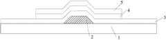
附图标记reference sign
1衬底基板 2栅电极 3栅绝缘层1
4第一金属氧化物半导体层 5第二金属氧化物半导体层4 first metal
6刻蚀阻挡层 7源漏金属层 8钝化层6
9像素电极9 pixel electrodes
具体实施方式Detailed ways
为使本发明的实施例要解决的技术问题、技术方案和优点更加清楚,下面将结合附图及具体实施例进行详细描述。In order to make the technical problems, technical solutions and advantages to be solved by the embodiments of the present invention clearer, the following will describe in detail with reference to the drawings and specific embodiments.
本发明的实施例提供一种阵列基板及其制作方法和显示装置,能够制备性能良好、稳定且具有高迁移率的有源层。Embodiments of the present invention provide an array substrate, a manufacturing method thereof, and a display device, capable of preparing an active layer with good performance, stability, and high mobility.
本发明实施例提供了一种阵列基板,所述阵列基板的有源层由至少两个金属氧化物半导体层组成,其中,靠近栅绝缘层的第一金属氧化物半导体层的迁移率大于靠近源漏金属层的第二金属氧化物半导体层的迁移率。An embodiment of the present invention provides an array substrate. The active layer of the array substrate is composed of at least two metal oxide semiconductor layers, wherein the mobility of the first metal oxide semiconductor layer close to the gate insulating layer is greater than that close to the source layer. Drain the mobility of the second metal oxide semiconductor layer from the metal layer.
本发明的阵列基板中,靠近栅绝缘层的第一金属氧化物半导体层作为载流子传输层具有较高的迁移率,而靠近源漏金属层的第二金属氧化物半导体层作为相对高电阻层具有较低的迁移率,可以起到降低漏电流、稳定TFT特性的作用。这样通过至少两个金属氧化物半导体层组合,最终可以制备性能良好、稳定且具有高迁移率的有源层。In the array substrate of the present invention, the first metal oxide semiconductor layer close to the gate insulating layer serves as a carrier transport layer with high mobility, while the second metal oxide semiconductor layer close to the source-drain metal layer serves as a relatively high-resistance The layer has a lower mobility, which can play a role in reducing leakage current and stabilizing TFT characteristics. In this way, by combining at least two metal oxide semiconductor layers, an active layer with good performance, stability and high mobility can be prepared finally.
本发明的阵列基板并不局限于采用两个金属氧化物半导体层形成有源层,有源层还可以具有三层以上的结构,只需要保证靠近栅绝缘层的那一层结构具有较高的迁移率,靠近源漏金属层的那一层结构具有较低的迁移率即可。在实际生产中,为了简化生产流程和节省生产成本,一般采用两个金属氧化物半导体层形成有源层。The array substrate of the present invention is not limited to using two metal oxide semiconductor layers to form the active layer, and the active layer can also have a structure of more than three layers. It only needs to ensure that the layer structure close to the gate insulating layer has a higher Mobility, the layer structure close to the source-drain metal layer should have a lower mobility. In actual production, in order to simplify the production process and save production costs, two metal oxide semiconductor layers are generally used to form the active layer.
进一步地,为了保证制备的有源层具有较高的迁移率,一般地,所采用的第一金属氧化物半导体层的迁移率大于30cm2/V*s;为了保证制备的有源层性能良好、稳定,一般地,所采用的第二金属氧化物半导体层的迁移率为8-10cm2/V*s。Further, in order to ensure that the prepared active layer has a high mobility, generally, the mobility of the first metal oxide semiconductor layer used is greater than 30 cm2 /V*s; in order to ensure that the prepared active layer has good performance , stability, generally, the mobility of the second metal oxide semiconductor layer used is 8-10 cm2 /V*s.
进一步地,所述第一金属氧化物半导体层的厚度可以为10nm-50nm,所述第二金属氧化物半导体层的厚度可以为10nm-50nm。Further, the thickness of the first metal oxide semiconductor layer may be 10nm-50nm, and the thickness of the second metal oxide semiconductor layer may be 10nm-50nm.
具体地,本发明的阵列基板中,第一金属氧化物半导体层可以采用ITZO,第二金属氧化物半导体层可以采用IGZO。IGZO的迁移率在10cm2/V*s左右,ITZO的迁移率可以达到30cm2/V*s以上,但是ITZO的漏电流比较大,这样将ITZO作为第一金属氧化物半导体层布置在栅绝缘层之上,由于其具有较高的迁移率可以作为载流子传输层;将IGZO作为第二金属氧化物半导体层布置在源漏金属层之下,由于其具有较低的迁移率可以作为相对高电阻层,起到降低漏电流、稳定TFT特性的作用。Specifically, in the array substrate of the present invention, ITZO may be used for the first metal oxide semiconductor layer, and IGZO may be used for the second metal oxide semiconductor layer. The mobility of IGZO is about 10cm2 /V*s, and the mobility of ITZO can reach more than 30cm2 /V*s, but the leakage current of ITZO is relatively large, so ITZO is arranged as the first metal oxide semiconductor layer on the gate insulation layer, because of its high mobility can be used as a carrier transport layer; IGZO as the second metal oxide semiconductor layer arranged under the source and drain metal layer, because of its low mobility can be used as a relative The high resistance layer plays the role of reducing leakage current and stabilizing TFT characteristics.
具体地,本发明的阵列基板可以包括:Specifically, the array substrate of the present invention may include:
衬底基板;Substrate substrate;
所述衬底基板上的栅电极和栅线;a gate electrode and a gate line on the base substrate;
所述栅电极和所述栅线上的所述栅绝缘层;the gate electrode and the gate insulating layer on the gate line;
所述栅绝缘层上的所述有源层,所述有源层由第一金属氧化物半导体层和第二金属氧化物半导体层组成;the active layer on the gate insulating layer, the active layer is composed of a first metal oxide semiconductor layer and a second metal oxide semiconductor layer;
所述有源层上的刻蚀阻挡层;an etch stop layer on the active layer;
所述刻蚀阻挡层上的由所述源漏金属层组成的漏电极、源电极和数据线;A drain electrode, a source electrode and a data line composed of the source-drain metal layer on the etching barrier layer;
所述漏电极、所述源电极和所述数据线上的钝化层,所述钝化层包括有对应所述漏电极的过孔;The passivation layer on the drain electrode, the source electrode and the data line, the passivation layer includes a via hole corresponding to the drain electrode;
所述钝化层上的像素电极,所述像素电极通过所述过孔与所述漏电极电连接。The pixel electrode on the passivation layer is electrically connected to the drain electrode through the via hole.
本发明实施例还提供了一种显示装置,包括如上任一实施例所述的阵列基板。其中,阵列基板的结构同上述实施例,在此不再赘述。另外,显示装置其他部分的结构可以参考现有技术,对此本文不再详细描述。该显示装置可以为:液晶面板、电子纸、液晶电视、液晶显示器、数码相框、手机、平板电脑等具有任何显示功能的产品或部件。An embodiment of the present invention also provides a display device, including the array substrate as described in any one of the above embodiments. Wherein, the structure of the array substrate is the same as that of the above-mentioned embodiments, and will not be repeated here. In addition, the structure of other parts of the display device can refer to the prior art, which will not be described in detail herein. The display device may be a product or component with any display function such as a liquid crystal panel, electronic paper, liquid crystal TV, liquid crystal display, digital photo frame, mobile phone, and tablet computer.
本发明实施例还提供了一种阵列基板的制作方法,包括:利用至少两个金属氧化物半导体层完成有源层的制作,其中,靠近栅绝缘层的第一金属氧化物半导体层的迁移率大于靠近源漏金属层的第二金属氧化物半导体层的迁移率。An embodiment of the present invention also provides a method for fabricating an array substrate, including: using at least two metal oxide semiconductor layers to complete the fabrication of the active layer, wherein the mobility of the first metal oxide semiconductor layer close to the gate insulating layer is Greater than the mobility of the second metal oxide semiconductor layer close to the source-drain metal layer.
本发明制作的阵列基板,靠近栅绝缘层的第一金属氧化物半导体层作为载流子传输层具有较高的迁移率,而靠近源漏金属层的第二金属氧化物半导体层作为相对高电阻层具有较低的迁移率,可以起到降低漏电流、稳定TFT特性的作用。这样通过至少两个金属氧化物半导体层组合,最终可以制备性能良好、稳定且具有高迁移率的有源层。In the array substrate produced by the present invention, the first metal oxide semiconductor layer close to the gate insulating layer serves as a carrier transport layer with high mobility, while the second metal oxide semiconductor layer close to the source-drain metal layer serves as a relatively high resistance The layer has a lower mobility, which can play a role in reducing leakage current and stabilizing TFT characteristics. In this way, by combining at least two metal oxide semiconductor layers, an active layer with good performance, stability and high mobility can be prepared finally.
本发明的制作方法并不局限于采用两个金属氧化物半导体层形成有源层,还可以利用三个以上的金属氧化物半导体层形成有源层,只需要保证靠近栅绝缘层的那一层金属氧化物半导体层具有较高的迁移率,靠近源漏金属层的那一层金属氧化物半导体层具有较低的迁移率即可。在实际生产中,为了简化生产流程和节省生产成本,一般采用两个金属氧化物半导体层形成有源层。The manufacturing method of the present invention is not limited to the use of two metal oxide semiconductor layers to form the active layer, and it is also possible to use more than three metal oxide semiconductor layers to form the active layer, as long as the layer close to the gate insulating layer needs to be guaranteed The metal oxide semiconductor layer has relatively high mobility, and the metal oxide semiconductor layer close to the source-drain metal layer only needs to have relatively low mobility. In actual production, in order to simplify the production process and save production costs, two metal oxide semiconductor layers are generally used to form the active layer.
进一步地,为了保证制备的有源层具有较高的迁移率,一般地,所采用的第一金属氧化物半导体层的迁移率大于30cm2/V*s;为了保证制备的有源层性能良好、稳定,一般地,所采用的第二金属氧化物半导体层的迁移率为8-10cm2/V*s。Further, in order to ensure that the prepared active layer has a high mobility, generally, the mobility of the first metal oxide semiconductor layer used is greater than 30 cm2 /V*s; in order to ensure that the prepared active layer has good performance , stability, generally, the mobility of the second metal oxide semiconductor layer used is 8-10 cm2 /V*s.
具体地,所述制作方法可以包括:Specifically, the manufacturing method may include:
在衬底基板上依次形成栅金属层和栅绝缘层,所述栅金属层包括栅电极和栅线的图形;sequentially forming a gate metal layer and a gate insulating layer on the base substrate, the gate metal layer including patterns of gate electrodes and gate lines;
在形成有所述栅绝缘层的衬底基板上形成有源层的图形,所述有源层由第一金属氧化物半导体层和第二金属氧化物半导体层组成;forming a pattern of an active layer on the substrate on which the gate insulating layer is formed, the active layer consisting of a first metal oxide semiconductor layer and a second metal oxide semiconductor layer;
在形成有所述有源层的衬底基板上形成刻蚀阻挡层的图形;forming a pattern of an etching stopper layer on the base substrate on which the active layer is formed;
在形成有所述刻蚀阻挡层的衬底基板上形成数据线、源电极和漏电极的图形;forming patterns of data lines, source electrodes, and drain electrodes on the base substrate on which the etching stopper layer is formed;
在形成有所述数据线、所述源电极和所述漏电极的衬底基板上形成钝化层的图形,所述钝化层的图形包括有对应所述漏电极的过孔;forming a pattern of a passivation layer on the base substrate on which the data line, the source electrode, and the drain electrode are formed, and the pattern of the passivation layer includes a via hole corresponding to the drain electrode;
在形成有所述钝化层的衬底基板上形成像素电极的图形,所述像素电极通过所述过孔与所述漏电极电连接。A pattern of a pixel electrode is formed on the base substrate on which the passivation layer is formed, and the pixel electrode is electrically connected to the drain electrode through the via hole.
其中,所述在形成有所述栅绝缘层的衬底基板上形成有源层的图形包括:Wherein, the pattern of forming the active layer on the base substrate on which the gate insulating layer is formed includes:
在形成有所述栅绝缘层的衬底基板上沉积所述第一金属氧化物半导体层;depositing the first metal oxide semiconductor layer on the substrate on which the gate insulating layer is formed;
在所述第一金属氧化物半导体层上沉积所述第二金属氧化物半导体层;depositing the second metal oxide semiconductor layer on the first metal oxide semiconductor layer;
在所述第二金属氧化物半导体层上涂覆光刻胶,通过构图工艺,形成由所述第一金属氧化物半导体层和所述第二金属氧化物半导体层组成的有源层的图形。A photoresist is coated on the second metal oxide semiconductor layer, and a pattern of an active layer composed of the first metal oxide semiconductor layer and the second metal oxide semiconductor layer is formed through a patterning process.
具体地,本发明的制作方法中,可以采用ITZO作为第一金属氧化物半导体层,可以采用IGZO作为第二金属氧化物半导体层。IGZO的迁移率在10cm2/V*s左右,ITZO的迁移率可以达到30cm2/V*s以上,但是ITZO的漏电流比较大,这样将ITZO作为第一金属氧化物半导体层布置在栅绝缘层之上,由于其具有较高的迁移率可以作为载流子传输层;将IGZO作为第二金属氧化物半导体层布置在源漏金属层之下,由于其具有较低的迁移率可以作为相对高电阻层,起到降低漏电流、稳定TFT特性的作用。Specifically, in the manufacturing method of the present invention, ITZO can be used as the first metal oxide semiconductor layer, and IGZO can be used as the second metal oxide semiconductor layer. The mobility of IGZO is about 10cm2 /V*s, and the mobility of ITZO can reach more than 30cm2 /V*s, but the leakage current of ITZO is relatively large, so ITZO is arranged as the first metal oxide semiconductor layer on the gate insulation layer, because of its high mobility can be used as a carrier transport layer; IGZO as the second metal oxide semiconductor layer arranged under the source and drain metal layer, because of its low mobility can be used as a relative The high resistance layer plays the role of reducing leakage current and stabilizing TFT characteristics.
下面结合具体的工艺流程对本实施例的阵列基板的制作方法进行进一步地介绍:The manufacturing method of the array substrate of this embodiment will be further introduced in combination with the specific process flow below:
如图1~图8所示,本发明的阵列基板的制作方法包括以下步骤:As shown in Figures 1 to 8, the manufacturing method of the array substrate of the present invention includes the following steps:
步骤a、提供一衬底基板,在衬底基板上形成由栅金属层组成的栅电极和栅线的图形;Step a, providing a base substrate, forming a pattern of gate electrodes and gate lines composed of a gate metal layer on the base substrate;
如图1所示,首先通过一次构图工艺在衬底基板1上形成由栅金属层组成的包括栅电极2和与栅电极2连接的栅线的图形。其中,衬底基板1可为玻璃基板或石英基板。As shown in FIG. 1 , firstly, a pattern consisting of a gate metal layer, including a
具体地,可以采用溅射或热蒸发的方法在衬底基板1上沉积一层栅金属层。栅金属层的材料可以是Cr、W、Ti、Ta、Mo、Al、Cu等金属及其合金,栅金属层也可以是由多层金属薄膜组成。在栅金属层上涂覆一层光刻胶,采用掩膜板对光刻胶进行曝光,使光刻胶形成光刻胶未保留区域和光刻胶保留区域,其中,光刻胶保留区域对应于栅线和栅电极2的图形所在区域,光刻胶未保留区域对应于上述图形以外的区域;进行显影处理,光刻胶未保留区域的光刻胶被完全去除,光刻胶保留区域的光刻胶厚度保持不变;通过刻蚀工艺完全刻蚀掉光刻胶未保留区域的栅金属薄膜,形成栅线和栅电极2的图形;剥离剩余的光刻胶。Specifically, a gate metal layer may be deposited on the
步骤b:如图2所示,在形成有栅电极2和栅线的衬底基板1上形成栅绝缘层3;Step b: as shown in FIG. 2 , forming a
具体地,可以采用等离子体增强化学气相沉积(PECVD)方法,在经过步骤a的衬底基板1上沉积厚度为
步骤c:在形成有栅绝缘层3的衬底基板1上沉积第一金属氧化物半导体层4和第二金属氧化物半导体层5;Step c: depositing a first metal
具体地,如图3所示,可以先在经过步骤b的衬底基板1上采用磁控溅射、热蒸发或其它成膜方法沉积ITZO作为第一金属氧化物半导体层4,具体地,ITZO的厚度可以为10nm-50nm,之后可以再沉积IGZO作为第二金属氧化物半导体层5,IGZO的厚度可以为10nm-50nm。Specifically, as shown in FIG. 3, ITZO can be deposited as the first metal
步骤d:如图4所示,在衬底基板1上形成有源层的图形;Step d: As shown in FIG. 4 , forming a pattern of the active layer on the
具体地,在第二金属氧化物半导体层5上涂覆光刻胶,对光刻胶进行曝光,使光刻胶形成光刻胶未保留区域和光刻胶保留区域;之后进行显影处理,光刻胶未保留区域的光刻胶被完全去除,光刻胶保留区域的光刻胶厚度保持不变;通过刻蚀工艺完全刻蚀掉光刻胶未保留区域的第一金属氧化物半导体层和第二金属氧化物半导体层,形成有源层的图形;剥离光刻胶保留区域的剩余的光刻胶。Specifically, a photoresist is coated on the second metal
步骤e:如图5所示,在衬底基板1上形成刻蚀阻挡层6的图形;Step e: As shown in FIG. 5 , forming a pattern of an
具体地,在经过步骤d的衬底基板1上采用磁控溅射、热蒸发或其它成膜方法沉积刻蚀阻挡层材料,其中,刻蚀阻挡层材料可以选用氧化物或者氮化物。在刻蚀阻挡层材料上涂覆一层光刻胶,采用掩膜板对光刻胶进行曝光,使光刻胶形成光刻胶未保留区域和光刻胶保留区域,其中,光刻胶保留区域对应于刻蚀阻挡层6的图形所在区域,光刻胶未保留区域对应于上述图形以外的区域;进行显影处理,光刻胶未保留区域的光刻胶被完全去除,光刻胶保留区域的光刻胶厚度保持不变;通过刻蚀工艺完全刻蚀掉光刻胶未保留区域的刻蚀阻挡层材料,形成刻蚀阻挡层6的图形;剥离剩余的光刻胶。Specifically, magnetron sputtering, thermal evaporation or other film-forming methods are used to deposit an etch stop layer material on the
步骤f:如图6所示,在衬底基板1上形成由源漏金属层7组成的源电极、漏电极和数据线的图形;Step f: As shown in FIG. 6 , forming patterns of source electrodes, drain electrodes and data lines composed of source and drain
具体地,在经过步骤e的衬底基板1上采用磁控溅射、热蒸发或其它成膜方法沉积一层源漏金属层7。源漏金属层7的材料可以是Cr、W、Ti、Ta、Mo、Al、Cu等金属及其合金,源漏金属层7也可以是由多层金属薄膜组成。在源漏金属层7上涂覆一层光刻胶,采用掩膜板对光刻胶进行曝光,使光刻胶形成光刻胶未保留区域和光刻胶保留区域,其中,光刻胶保留区域对应于源电极、漏电极和数据线的图形所在区域,光刻胶未保留区域对应于上述图形以外的区域;进行显影处理,光刻胶未保留区域的光刻胶被完全去除,光刻胶保留区域的光刻胶厚度保持不变;通过刻蚀工艺完全刻蚀掉光刻胶未保留区域的源漏金属薄膜,形成源电极、漏电极和数据线的图形;剥离剩余的光刻胶。Specifically, a source-
步骤g:如图7所示,在衬底基板1上形成钝化层8的图形;Step g: As shown in FIG. 7 , forming a pattern of a
具体地,在经过步骤f的衬底基板1上采用磁控溅射、热蒸发或其它成膜方法沉积厚度为
步骤h:如图8所示,在衬底基板1上形成像素电极9的图形,像素电极9通过过孔与漏电极连接。Step h: As shown in FIG. 8 , a pattern of pixel electrodes 9 is formed on the
具体地,在经过步骤g的衬底基板1上采用磁控溅射、热蒸发或其它成膜方法沉积厚度为
经过上述步骤a-h即可得到如图8所示的本实施例的阵列基板,本实施例的技术方案采用两个金属氧化物半导体层制备有源层,其中,靠近栅绝缘层的第一金属氧化物半导体层作为载流子传输层具有较高的迁移率,而靠近源漏金属层的第二金属氧化物半导体层作为相对高电阻层具有较低的迁移率,可以起到降低漏电流、稳定TFT特性的作用。这样通过至少两个金属氧化物半导体层组合,最终可以制备性能良好、稳定且具有高迁移率的有源层。After the above steps a-h, the array substrate of this embodiment as shown in Figure 8 can be obtained. The technical solution of this embodiment uses two metal oxide semiconductor layers to prepare the active layer, wherein the first metal oxide layer close to the gate insulating layer The material semiconductor layer has a high mobility as a carrier transport layer, and the second metal oxide semiconductor layer close to the source and drain metal layer has a relatively low mobility as a relatively high resistance layer, which can reduce leakage current and stabilize Effect of TFT characteristics. In this way, by combining at least two metal oxide semiconductor layers, an active layer with good performance, stability and high mobility can be prepared finally.
以上所述是本发明的优选实施方式,应当指出,对于本技术领域的普通技术人员来说,在不脱离本发明所述原理的前提下,还可以作出若干改进和润饰,这些改进和润饰也应视为本发明的保护范围。The above description is a preferred embodiment of the present invention, it should be pointed out that for those of ordinary skill in the art, without departing from the principle of the present invention, some improvements and modifications can also be made, and these improvements and modifications can also be made. It should be regarded as the protection scope of the present invention.
Claims (10)
Priority Applications (3)
| Application Number | Priority Date | Filing Date | Title |
|---|---|---|---|
| CN2013103198024ACN103412450A (en) | 2013-07-26 | 2013-07-26 | Array substrate, manufacturing method thereof and display device |
| PCT/CN2013/089674WO2015010427A1 (en) | 2013-07-26 | 2013-12-17 | Array substrate and manufacturing method therefor, and display device |
| US14/381,646US9646997B2 (en) | 2013-07-26 | 2013-12-17 | Array substrate, method for manufacturing the same and display device |
Applications Claiming Priority (1)
| Application Number | Priority Date | Filing Date | Title |
|---|---|---|---|
| CN2013103198024ACN103412450A (en) | 2013-07-26 | 2013-07-26 | Array substrate, manufacturing method thereof and display device |
Publications (1)
| Publication Number | Publication Date |
|---|---|
| CN103412450Atrue CN103412450A (en) | 2013-11-27 |
Family
ID=49605477
Family Applications (1)
| Application Number | Title | Priority Date | Filing Date |
|---|---|---|---|
| CN2013103198024APendingCN103412450A (en) | 2013-07-26 | 2013-07-26 | Array substrate, manufacturing method thereof and display device |
Country Status (3)
| Country | Link |
|---|---|
| US (1) | US9646997B2 (en) |
| CN (1) | CN103412450A (en) |
| WO (1) | WO2015010427A1 (en) |
Cited By (11)
| Publication number | Priority date | Publication date | Assignee | Title |
|---|---|---|---|---|
| CN103943638A (en)* | 2014-04-15 | 2014-07-23 | 京东方科技集团股份有限公司 | Array substrate, manufacturing method of array substrate and display device |
| CN103943639A (en)* | 2014-04-15 | 2014-07-23 | 京东方科技集团股份有限公司 | Array substrate, manufacturing method thereof, and display device |
| WO2015010427A1 (en)* | 2013-07-26 | 2015-01-29 | 京东方科技集团股份有限公司 | Array substrate and manufacturing method therefor, and display device |
| CN104332474A (en)* | 2014-09-02 | 2015-02-04 | 重庆京东方光电科技有限公司 | Array substrate and preparation method thereof, and display device |
| CN105304651A (en)* | 2015-11-25 | 2016-02-03 | 深圳市华星光电技术有限公司 | Array substrate, display, and preparation method of array substrate |
| WO2016019649A1 (en)* | 2014-08-06 | 2016-02-11 | 京东方科技集团股份有限公司 | Display device, array substrate and manufacturing method therefor, and thin-film transistor and manufacturing method therefor |
| KR20160070881A (en)* | 2014-12-10 | 2016-06-21 | 삼성디스플레이 주식회사 | Thin film transistor |
| CN110010626A (en)* | 2019-04-11 | 2019-07-12 | 京东方科技集团股份有限公司 | Display substrate, manufacturing method thereof, and display device |
| CN111403336A (en)* | 2020-03-31 | 2020-07-10 | 成都中电熊猫显示科技有限公司 | Array substrate, display panel and manufacturing method of array substrate |
| CN114420762A (en)* | 2020-10-28 | 2022-04-29 | 京东方科技集团股份有限公司 | Oxide thin film transistor, manufacturing method thereof and display device |
| CN115295564A (en)* | 2022-09-27 | 2022-11-04 | 广州华星光电半导体显示技术有限公司 | Array substrates and display panels |
Families Citing this family (4)
| Publication number | Priority date | Publication date | Assignee | Title |
|---|---|---|---|---|
| CN104392928A (en)* | 2014-11-20 | 2015-03-04 | 深圳市华星光电技术有限公司 | Manufacturing method of film transistor |
| KR102106366B1 (en)* | 2015-11-25 | 2020-05-04 | 가부시키가이샤 아루박 | Thin film transistor, oxide semiconductor film and sputtering target |
| JP2019067791A (en)* | 2017-09-28 | 2019-04-25 | シャープ株式会社 | Semiconductor device |
| CN112909025A (en)* | 2021-02-09 | 2021-06-04 | 福建华佳彩有限公司 | Array substrate and preparation method thereof |
Citations (2)
| Publication number | Priority date | Publication date | Assignee | Title |
|---|---|---|---|---|
| WO2012091297A1 (en)* | 2010-12-30 | 2012-07-05 | 주성엔지니어링㈜ | Thin-film transistor and method for manufacturing same |
| CN203351574U (en)* | 2013-07-26 | 2013-12-18 | 京东方科技集团股份有限公司 | Array substrate and display device |
Family Cites Families (7)
| Publication number | Priority date | Publication date | Assignee | Title |
|---|---|---|---|---|
| KR101513601B1 (en) | 2008-03-07 | 2015-04-21 | 삼성전자주식회사 | transistor |
| KR101497425B1 (en) | 2008-08-28 | 2015-03-03 | 삼성디스플레이 주식회사 | Liquid crystal display device and manufacturing method thereof |
| KR102436902B1 (en)* | 2010-04-02 | 2022-08-25 | 가부시키가이샤 한도오따이 에네루기 켄큐쇼 | Semiconductor device |
| KR20130111874A (en)* | 2012-04-02 | 2013-10-11 | 삼성디스플레이 주식회사 | Thin film transistor, thin film transistor array panel and display device including the same, and manufacturing method of thin film transistor |
| CN202957251U (en) | 2012-12-13 | 2013-05-29 | 京东方科技集团股份有限公司 | A kind of thin film transistor, array substrate and display device |
| DE112013006219T5 (en)* | 2012-12-25 | 2015-09-24 | Semiconductor Energy Laboratory Co., Ltd. | Semiconductor device and its manufacturing method |
| CN103412450A (en)* | 2013-07-26 | 2013-11-27 | 京东方科技集团股份有限公司 | Array substrate, manufacturing method thereof and display device |
- 2013
- 2013-07-26CNCN2013103198024Apatent/CN103412450A/enactivePending
- 2013-12-17WOPCT/CN2013/089674patent/WO2015010427A1/enactiveApplication Filing
- 2013-12-17USUS14/381,646patent/US9646997B2/enactiveActive
Patent Citations (2)
| Publication number | Priority date | Publication date | Assignee | Title |
|---|---|---|---|---|
| WO2012091297A1 (en)* | 2010-12-30 | 2012-07-05 | 주성엔지니어링㈜ | Thin-film transistor and method for manufacturing same |
| CN203351574U (en)* | 2013-07-26 | 2013-12-18 | 京东方科技集团股份有限公司 | Array substrate and display device |
Cited By (16)
| Publication number | Priority date | Publication date | Assignee | Title |
|---|---|---|---|---|
| WO2015010427A1 (en)* | 2013-07-26 | 2015-01-29 | 京东方科技集团股份有限公司 | Array substrate and manufacturing method therefor, and display device |
| US9646997B2 (en) | 2013-07-26 | 2017-05-09 | Boe Technology Group Co., Ltd. | Array substrate, method for manufacturing the same and display device |
| CN103943639A (en)* | 2014-04-15 | 2014-07-23 | 京东方科技集团股份有限公司 | Array substrate, manufacturing method thereof, and display device |
| CN103943638A (en)* | 2014-04-15 | 2014-07-23 | 京东方科技集团股份有限公司 | Array substrate, manufacturing method of array substrate and display device |
| WO2016019649A1 (en)* | 2014-08-06 | 2016-02-11 | 京东方科技集团股份有限公司 | Display device, array substrate and manufacturing method therefor, and thin-film transistor and manufacturing method therefor |
| CN104332474A (en)* | 2014-09-02 | 2015-02-04 | 重庆京东方光电科技有限公司 | Array substrate and preparation method thereof, and display device |
| CN104332474B (en)* | 2014-09-02 | 2017-10-31 | 重庆京东方光电科技有限公司 | A kind of array base palte and preparation method thereof and display device |
| KR102260886B1 (en)* | 2014-12-10 | 2021-06-07 | 삼성디스플레이 주식회사 | Thin film transistor |
| KR20160070881A (en)* | 2014-12-10 | 2016-06-21 | 삼성디스플레이 주식회사 | Thin film transistor |
| CN105702740A (en)* | 2014-12-10 | 2016-06-22 | 三星显示有限公司 | Thin film transistor with improved electrical characteristics |
| CN105304651A (en)* | 2015-11-25 | 2016-02-03 | 深圳市华星光电技术有限公司 | Array substrate, display, and preparation method of array substrate |
| CN105304651B (en)* | 2015-11-25 | 2018-07-20 | 深圳市华星光电技术有限公司 | The preparation method of array substrate, display and array substrate |
| CN110010626A (en)* | 2019-04-11 | 2019-07-12 | 京东方科技集团股份有限公司 | Display substrate, manufacturing method thereof, and display device |
| CN111403336A (en)* | 2020-03-31 | 2020-07-10 | 成都中电熊猫显示科技有限公司 | Array substrate, display panel and manufacturing method of array substrate |
| CN114420762A (en)* | 2020-10-28 | 2022-04-29 | 京东方科技集团股份有限公司 | Oxide thin film transistor, manufacturing method thereof and display device |
| CN115295564A (en)* | 2022-09-27 | 2022-11-04 | 广州华星光电半导体显示技术有限公司 | Array substrates and display panels |
Also Published As
| Publication number | Publication date |
|---|---|
| US9646997B2 (en) | 2017-05-09 |
| US20160233250A1 (en) | 2016-08-11 |
| WO2015010427A1 (en) | 2015-01-29 |
Similar Documents
| Publication | Publication Date | Title |
|---|---|---|
| CN103412450A (en) | Array substrate, manufacturing method thereof and display device | |
| CN102751240B (en) | Thin film transistor array substrate, manufacturing method thereof, display panel and display device | |
| CN103700665B (en) | Metal oxide thin-film transistor array base palte and preparation method thereof, display unit | |
| CN103236440B (en) | Thin-film transistor, array base palte and manufacture method thereof, display unit | |
| CN102709234B (en) | Thin-film transistor array base-plate and manufacture method thereof and electronic device | |
| CN105070684B (en) | Preparation method of array substrate, array substrate and display device | |
| CN103887245B (en) | A kind of manufacture method of array base palte | |
| CN104078470B (en) | Array substrate, producing method thereof, display device | |
| CN103545319A (en) | Low-temperature polysilicon thin film transistor array substrate, manufacturing method thereof, and display device | |
| CN202473925U (en) | Top gate type TFT (Thin Film Transistor) array substrate and display device | |
| CN102881598B (en) | The manufacture method of thin-film transistor, the manufacture method of array base palte and display unit | |
| CN104779302A (en) | Thin film transistor and manufacturing method, array substrate and display device thereof | |
| CN104952932A (en) | Thin-film transistor, array substrate, manufacturing method of thin-film transistor, manufacturing method of array substrate, and display device | |
| CN102654698A (en) | Liquid crystal display array substrate and manufacturing method thereof as well as liquid crystal display | |
| CN106784014A (en) | Thin film transistor (TFT) and preparation method thereof, display base plate, display device | |
| CN102637648B (en) | Thin film transistor liquid crystal display, array substrate and manufacturing method thereof | |
| CN103700670B (en) | Array base palte and preparation method thereof, display device | |
| CN103700628A (en) | Manufacturing method of array substrate, array substrate and display device | |
| CN106449667A (en) | Array substrate, manufacturing method thereof and display device | |
| CN104167365A (en) | Metal oxide thin-film transistor, array substrate, manufacturing method of metal oxide thin-film transistor and display device | |
| CN104934443A (en) | Array substrate, manufacture method thereof, and display device | |
| CN103048840B (en) | Array substrate, manufacture method of array substrate, liquid crystal display panel and display device | |
| CN103337462B (en) | Preparation method of thin film transistor | |
| CN103700663B (en) | A kind of array base palte and preparation method thereof, display device | |
| CN103456747A (en) | Array substrate, manufacturing method of array substrate and display device |
Legal Events
| Date | Code | Title | Description |
|---|---|---|---|
| C06 | Publication | ||
| PB01 | Publication | ||
| C10 | Entry into substantive examination | ||
| SE01 | Entry into force of request for substantive examination | ||
| C12 | Rejection of a patent application after its publication | ||
| RJ01 | Rejection of invention patent application after publication | Application publication date:20131127 |