CN103401424A - Systems and methods for adjusting output current of a power conversion system - Google Patents
Systems and methods for adjusting output current of a power conversion systemDownload PDFInfo
- Publication number
- CN103401424A CN103401424ACN201310306106XACN201310306106ACN103401424ACN 103401424 ACN103401424 ACN 103401424ACN 201310306106X ACN201310306106X ACN 201310306106XACN 201310306106 ACN201310306106 ACN 201310306106ACN 103401424 ACN103401424 ACN 103401424A
- Authority
- CN
- China
- Prior art keywords
- terminal
- voltage
- signal
- transistor
- resistor
- Prior art date
- Legal status (The legal status is an assumption and is not a legal conclusion. Google has not performed a legal analysis and makes no representation as to the accuracy of the status listed.)
- Granted
Links
Images


Classifications
- H—ELECTRICITY
- H02—GENERATION; CONVERSION OR DISTRIBUTION OF ELECTRIC POWER
- H02M—APPARATUS FOR CONVERSION BETWEEN AC AND AC, BETWEEN AC AND DC, OR BETWEEN DC AND DC, AND FOR USE WITH MAINS OR SIMILAR POWER SUPPLY SYSTEMS; CONVERSION OF DC OR AC INPUT POWER INTO SURGE OUTPUT POWER; CONTROL OR REGULATION THEREOF
- H02M3/00—Conversion of DC power input into DC power output
- H02M3/22—Conversion of DC power input into DC power output with intermediate conversion into AC
- H02M3/24—Conversion of DC power input into DC power output with intermediate conversion into AC by static converters
- H02M3/28—Conversion of DC power input into DC power output with intermediate conversion into AC by static converters using discharge tubes with control electrode or semiconductor devices with control electrode to produce the intermediate AC
- H02M3/325—Conversion of DC power input into DC power output with intermediate conversion into AC by static converters using discharge tubes with control electrode or semiconductor devices with control electrode to produce the intermediate AC using devices of a triode or a transistor type requiring continuous application of a control signal
- H02M3/335—Conversion of DC power input into DC power output with intermediate conversion into AC by static converters using discharge tubes with control electrode or semiconductor devices with control electrode to produce the intermediate AC using devices of a triode or a transistor type requiring continuous application of a control signal using semiconductor devices only
- H02M3/33507—Conversion of DC power input into DC power output with intermediate conversion into AC by static converters using discharge tubes with control electrode or semiconductor devices with control electrode to produce the intermediate AC using devices of a triode or a transistor type requiring continuous application of a control signal using semiconductor devices only with automatic control of the output voltage or current, e.g. flyback converters
- H—ELECTRICITY
- H02—GENERATION; CONVERSION OR DISTRIBUTION OF ELECTRIC POWER
- H02M—APPARATUS FOR CONVERSION BETWEEN AC AND AC, BETWEEN AC AND DC, OR BETWEEN DC AND DC, AND FOR USE WITH MAINS OR SIMILAR POWER SUPPLY SYSTEMS; CONVERSION OF DC OR AC INPUT POWER INTO SURGE OUTPUT POWER; CONTROL OR REGULATION THEREOF
- H02M1/00—Details of apparatus for conversion
- H02M1/08—Circuits specially adapted for the generation of control voltages for semiconductor devices incorporated in static converters
- H—ELECTRICITY
- H05—ELECTRIC TECHNIQUES NOT OTHERWISE PROVIDED FOR
- H05B—ELECTRIC HEATING; ELECTRIC LIGHT SOURCES NOT OTHERWISE PROVIDED FOR; CIRCUIT ARRANGEMENTS FOR ELECTRIC LIGHT SOURCES, IN GENERAL
- H05B45/00—Circuit arrangements for operating light-emitting diodes [LED]
- H05B45/30—Driver circuits
- H05B45/32—Pulse-control circuits
- H05B45/325—Pulse-width modulation [PWM]
- H—ELECTRICITY
- H05—ELECTRIC TECHNIQUES NOT OTHERWISE PROVIDED FOR
- H05B—ELECTRIC HEATING; ELECTRIC LIGHT SOURCES NOT OTHERWISE PROVIDED FOR; CIRCUIT ARRANGEMENTS FOR ELECTRIC LIGHT SOURCES, IN GENERAL
- H05B45/00—Circuit arrangements for operating light-emitting diodes [LED]
- H05B45/30—Driver circuits
- H05B45/37—Converter circuits
- H05B45/3725—Switched mode power supply [SMPS]
- H05B45/38—Switched mode power supply [SMPS] using boost topology
- H—ELECTRICITY
- H05—ELECTRIC TECHNIQUES NOT OTHERWISE PROVIDED FOR
- H05B—ELECTRIC HEATING; ELECTRIC LIGHT SOURCES NOT OTHERWISE PROVIDED FOR; CIRCUIT ARRANGEMENTS FOR ELECTRIC LIGHT SOURCES, IN GENERAL
- H05B45/00—Circuit arrangements for operating light-emitting diodes [LED]
- H05B45/30—Driver circuits
- H05B45/37—Converter circuits
- H05B45/3725—Switched mode power supply [SMPS]
- H05B45/382—Switched mode power supply [SMPS] with galvanic isolation between input and output
- H—ELECTRICITY
- H02—GENERATION; CONVERSION OR DISTRIBUTION OF ELECTRIC POWER
- H02M—APPARATUS FOR CONVERSION BETWEEN AC AND AC, BETWEEN AC AND DC, OR BETWEEN DC AND DC, AND FOR USE WITH MAINS OR SIMILAR POWER SUPPLY SYSTEMS; CONVERSION OF DC OR AC INPUT POWER INTO SURGE OUTPUT POWER; CONTROL OR REGULATION THEREOF
- H02M1/00—Details of apparatus for conversion
- H02M1/0003—Details of control, feedback or regulation circuits
- H02M1/0009—Devices or circuits for detecting current in a converter
- H—ELECTRICITY
- H02—GENERATION; CONVERSION OR DISTRIBUTION OF ELECTRIC POWER
- H02M—APPARATUS FOR CONVERSION BETWEEN AC AND AC, BETWEEN AC AND DC, OR BETWEEN DC AND DC, AND FOR USE WITH MAINS OR SIMILAR POWER SUPPLY SYSTEMS; CONVERSION OF DC OR AC INPUT POWER INTO SURGE OUTPUT POWER; CONTROL OR REGULATION THEREOF
- H02M1/00—Details of apparatus for conversion
- H02M1/0003—Details of control, feedback or regulation circuits
- H02M1/0016—Control circuits providing compensation of output voltage deviations using feedforward of disturbance parameters
- H02M1/0022—Control circuits providing compensation of output voltage deviations using feedforward of disturbance parameters the disturbance parameters being input voltage fluctuations
- H—ELECTRICITY
- H02—GENERATION; CONVERSION OR DISTRIBUTION OF ELECTRIC POWER
- H02M—APPARATUS FOR CONVERSION BETWEEN AC AND AC, BETWEEN AC AND DC, OR BETWEEN DC AND DC, AND FOR USE WITH MAINS OR SIMILAR POWER SUPPLY SYSTEMS; CONVERSION OF DC OR AC INPUT POWER INTO SURGE OUTPUT POWER; CONTROL OR REGULATION THEREOF
- H02M1/00—Details of apparatus for conversion
- H02M1/36—Means for starting or stopping converters
Landscapes
- Engineering & Computer Science (AREA)
- Power Engineering (AREA)
- Dc-Dc Converters (AREA)
- Amplifiers (AREA)
Abstract
Description
Translated fromChinese技术领域technical field
本发明涉及集成电路。更具体地,本发明提供了用于电流调整的系统和方法。仅仅作为示例,本发明已应用于电源变换系统。但是将认识到,本发明具有更广泛的应用范围。The present invention relates to integrated circuits. More specifically, the present invention provides systems and methods for current regulation. Merely by way of example, the invention has been applied to power conversion systems. It will be appreciated, however, that the invention has a much broader range of applicability.
背景技术Background technique
发光二极管(LED)被广泛用于照明应用。通常,流经LED的电流需要近似恒定。LED的输出电流精度常常被用于确定LED照明系统的恒流特性。Light emitting diodes (LEDs) are widely used in lighting applications. Typically, the current through the LED needs to be approximately constant. The output current accuracy of LEDs is often used to determine the constant current characteristics of LED lighting systems.
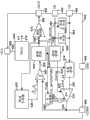
图1是传统的用于LED照明的电源变换系统的简化示图。该电源变换系统100包括控制器102、电阻器104,124,126和132、电容器106,120和134、二极管108、包含初级绕组112、次级绕组114和辅助绕组116的变压器110、功率开关128、电流感测电阻器130以及整流二极管118。控制器102包括端子138、140、142、144、146和148。例如,功率开关128是双极面结型晶体管。在另一示例中,功率开关128是MOS晶体管。FIG. 1 is a simplified diagram of a conventional power conversion system for LED lighting. The
交流(AC)输入电压152被施加给系统100。与AC输入电压152相关联的体电压(bulk voltage)150(例如,不小于0V的经整流电压)被电阻器104接收。电容器106响应于体电压150被充电,并且电压154在端子138(例如,端子VCC)处被提供给控制器102。如果电压154的大小大于预定阈值电压(例如,欠压锁定阈值),则控制器102开始正常工作,并且通过端子142(例如,端子GATE)输出驱动信号156。例如,驱动信号156是与开关频率和占空比相关联的脉宽调制(PWM)信号。开关128响应于驱动信号156而闭合(例如,接通)或断开(例如,关断),以使得输出电流158被调整为近似恒定。An alternating current (AC)
当开关128响应于驱动信号156闭合(例如,接通)时辅助绕组116通过二极管108对电容器106充电,以使得控制器102可以正常工作。反馈信号160通过端子140(例如,端子FB)被提供给控制器102,以便检测次级绕组118的退磁过程的结束以用于利用控制器102中的内部误差放大器来对电容器134充电或放电。电阻器130用于检测流经初级绕组112的初级电流162,并且电流感测信号164通过端子144(例如,端子CS)被提供给控制器102以便在每个开关周期期间被处理。电流感测信号164的峰值大小被采样并被提供给内部误差放大器。电容器120被用来使输出电压168保持稳定。When the
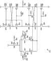
图2是示出作为系统100一部分的控制器102的简化传统示图。该控制器102包括振荡器202、欠压锁定(UVLO)组件204、调制组件206、逻辑控制器208、驱动组件210、退磁检测器212、误差放大器216和电流感测组件214。FIG. 2 is a simplified conventional diagram
如图2所示,UVLO组件204检测信号154并且输出信号218。如果信号154的大小大于预定阈值,则控制器102开始正常工作。如果信号154的大小小于预定阈值,则控制器102关断。误差放大器216接收参考信号222和来自电流感测组件214的信号220,并且向调制组件206输出放大信号224。调制组件206还接收来自振荡器202的信号228并且输出调制信号226,该调制信号226是PWM信号。例如,信号228是斜坡信号并且在每个开关时间周期期间线性地或非线性地增大到峰值大小。在另一示例中,调制信号226具有固定开关频率并且信号226的占空比基于信号224与信号228之间的比较来确定。逻辑控制器208处理调制信号226并且向驱动组件210输出控制信号230,驱动组件210生成信号156以接通或关断开关128。退磁检测器212检测反馈信号160并且输出信号232用于确定次级绕组114的退磁过程的开始和结束。As shown in FIG. 2 ,
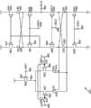
图3是示出作为控制器102的部分的电流感测组件214和误差放大器216的简化传统示图。电流感测组件214包括开关302和电容器304。误差放大器216包括开关306和308、运算放大器310。FIG. 3 is a simplified conventional diagram showing the
如图3所示,电流感测组件214对电流感测信号164采样并且误差放大器216放大信号220与参考信号222之差。具体地,开关302响应于信号314被闭合(例如接通)或断开(例如,关断)以便在不同开关时间周期中对电流感测信号164的峰值大小进行采样。如果开关302响应于信号314闭合(例如接通)并且开关306响应于来自退磁检测器212的信号232断开(例如,关断),则电容器304被充电并且信号220的大小增大。如果开关306响应于信号232闭合(例如接通),则开关308响应于信号312断开(例如,关断)并且信号220与参考信号222之差被放大器310放大。例如,在次级绕组114的退磁过程期间,信号232为逻辑高电平。开关306保持闭合(例如接通)并且开关308保持断开(例如,关断)。放大器310与电容器134一起执行与信号220相关联的积分。As shown in FIG. 3 , the
在稳定的正常工作下,根据下式来确定平均输出电流而无需考虑任何误差电流:Under stable normal operation, the average output current is determined according to the following formula without considering any error current:
其中,N表示初级绕组112与次级绕组114之间的匝数比,Vref_ea表示参考信号222并且Rcs表示电阻器130的电阻。Where N represents the turns ratio between the
但是,系统100在将输出电流调整为近似恒定时存在问题。因此,改善调整电源变换系统的输出电流的技术变得非常重要。However,
发明内容Contents of the invention
本发明涉及集成电路。更具体地,本发明提供了用于电流调整的系统和方法。仅仅作为示例,本发明已应用于电源变换系统。但是将认识到,本发明具有更广泛的应用范围。The present invention relates to integrated circuits. More specifically, the present invention provides systems and methods for current regulation. Merely by way of example, the invention has been applied to power conversion systems. It will be appreciated, however, that the invention has a much broader range of applicability.
根据一个实施例,一种用于处理与电源变换系统的电流相关联的输入信号和参考信号的误差放大器包括:第一运算放大器、第二运算放大器、第一晶体管、第二晶体管、电流镜组件、开关、第一电阻器和第二电阻器。第一运算放大器包括第一输入端子、第二输入端子和第一输出端子,所述第一输入端子被配置为接收参考信号。第一晶体管包括第一晶体管端子、第二晶体管端子和第三晶体管端子,所述第一晶体管端子被配置为从所述第一输出端子接收第一放大信号,所述第三晶体管端子被耦合到所述第二输入端子。第二运算放大器包括第三输入端子、第四输入端子和第二输出端子,所述第三输入端子被配置为接收与流经电源变换系统的初级绕组的电流相关联的输入信号。第二晶体管包括第四晶体管端子、第五晶体管端子和第六晶体管端子,所述第四晶体管端子被配置为从所述第二输出端子接收第二放大信号,所述第六晶体管端子被耦合到所述第四输入端子。电流镜组件包括第一组件端子和第二组件端子,所述第一组件端子被耦合到所述第二晶体管端子。开关包括第一开关端子和第二开关端子,所述第一开关端子被耦合到所述第二组件端子,所述第二开关端子被耦合到所述第五晶体管端子。第一电阻器包括第一电阻器端子和第二电阻器端子,所述第一电阻器与第一电阻相关联,所述第一电阻器端子被耦合到所述第二输入端子。第二电阻器包括第三电阻器端子和第四电阻器端子,所述第二电阻器与第二电阻相关联,所述第三电阻器端子被耦合到所述第四输入端子。所述第一电阻的大小大于所述第二电阻。所述第二组件端子被配置为至少基于与所述参考信号和所述输入信号相关联的信息输出输出信号。According to one embodiment, an error amplifier for processing an input signal and a reference signal associated with a current of a power conversion system includes: a first operational amplifier, a second operational amplifier, a first transistor, a second transistor, a current mirror assembly , switch, first resistor and second resistor. The first operational amplifier includes a first input terminal, a second input terminal and a first output terminal, the first input terminal being configured to receive a reference signal. The first transistor includes a first transistor terminal configured to receive a first amplified signal from the first output terminal, a second transistor terminal and a third transistor terminal, the third transistor terminal being coupled to the second input terminal. The second operational amplifier includes a third input terminal, a fourth input terminal, and a second output terminal, the third input terminal being configured to receive an input signal associated with current flowing through the primary winding of the power conversion system. The second transistor includes a fourth transistor terminal, a fifth transistor terminal and a sixth transistor terminal, the fourth transistor terminal being configured to receive a second amplified signal from the second output terminal, the sixth transistor terminal being coupled to the fourth input terminal. A current mirror component includes a first component terminal and a second component terminal, the first component terminal being coupled to the second transistor terminal. A switch includes a first switch terminal coupled to the second component terminal and a second switch terminal coupled to the fifth transistor terminal. The first resistor includes a first resistor terminal and a second resistor terminal, the first resistor being associated with the first resistance, the first resistor terminal being coupled to the second input terminal. The second resistor includes a third resistor terminal and a fourth resistor terminal, the second resistor being associated with the second resistance, the third resistor terminal being coupled to the fourth input terminal. The magnitude of the first resistor is greater than that of the second resistor. The second component terminal is configured to output an output signal based at least on information associated with the reference signal and the input signal.
根据另一实施例,一种用于调整电源变换系统的系统控制器包括:第一控制器端子,被配置为接收与第一电流相关联的第一电压,所述第一电流与电源变换系统的输入电压有关;补偿组件,被耦合到所述第一控制器端子并被配置为如果所述第一电压满足一个或多个第一条件则至少基于与所述第一电流相关联的信息生成补偿电流;以及第二控制器端子,被耦合到所述补偿组件并被配置为至少基于与所述补偿电流相关联的信息提供补偿电压,所述补偿电压的大小等于所述补偿电流乘以补偿电阻,所述补偿电阻与补偿电阻器相关联。该系统控制器还包括:电流感测组件,被配置为接收第二电压并且生成第二输出信号,所述第二电压的大小等于第三电压与所述补偿电压之和,所述第三电压与流经所述电源变换系统的初级绕组的第二电流成比例;以及误差放大器,被配置为接收所述输出信号和参考信号,至少基于与所述输出信号和所述参考信号相关联的信息生成放大信号,并且输出所述放大信号以影响与所述第二电流相关联的开关。According to another embodiment, a system controller for regulating a power conversion system includes: a first controller terminal configured to receive a first voltage associated with a first current, the first current being related to a power conversion system related to the input voltage; a compensation component coupled to the first controller terminal and configured to generate, based at least on information associated with the first current, if the first voltage satisfies one or more first conditions a compensation current; and a second controller terminal coupled to the compensation component and configured to provide a compensation voltage having a magnitude equal to the compensation current multiplied by a compensation current based at least on information associated with the compensation current A resistor, the compensation resistor is associated with the compensation resistor. The system controller further includes: a current sensing component configured to receive a second voltage equal to a sum of a third voltage and the compensation voltage, and generate a second output signal, the third voltage proportional to a second current flowing through a primary winding of the power conversion system; and an error amplifier configured to receive the output signal and a reference signal based at least on information associated with the output signal and the reference signal An amplified signal is generated and output to affect a switch associated with the second current.
根据又一实施例,一种用于调整电源变换系统的系统控制器包括:第一控制器端子,被配置为接收与电源变换系统的输出电压相关联的反馈信号;补偿组件,被耦合到所述第一控制器端子并被配置为在所述电源变换系统的退磁过程期间对所述反馈信号采样并且至少基于与所述第一电流相关联的信息生成补偿电流;以及第二控制器端子,被耦合到所述补偿组件并被配置为至少基于与所述补偿电流相关联的信息提供补偿电压,所述补偿电压的大小等于所述补偿电流乘以补偿电阻,所述补偿电阻与补偿电阻器相关联。另外,该系统控制器包括:电流感测组件,被配置为接收输入电压并且生成输出信号,所述输入电压的大小等于第一电压与所述补偿电压之和,所述第一电压与流经所述电源变换系统的初级绕组的第一电流成比例;以及误差放大器,被配置为接收所述输出信号和参考信号,至少基于与所述输出信号和所述参考信号相关联的信息生成放大信号,并且输出所述放大信号以影响与所述第一电流相关联的开关。According to yet another embodiment, a system controller for regulating a power conversion system includes: a first controller terminal configured to receive a feedback signal associated with an output voltage of the power conversion system; a compensation component coupled to the the first controller terminal and configured to sample the feedback signal and generate a compensation current based at least on information associated with the first current during a demagnetization process of the power conversion system; and a second controller terminal, coupled to the compensation component and configured to provide a compensation voltage equal to the compensation current multiplied by a compensation resistance based at least on information associated with the compensation current, the compensation resistance being equal to the compensation resistor Associated. In addition, the system controller includes: a current sensing component configured to receive an input voltage equal to the sum of a first voltage and the compensation voltage, the first voltage and the current flowing through it and generate an output signal. a first current proportional to a primary winding of the power conversion system; and an error amplifier configured to receive the output signal and a reference signal, generate an amplified signal based at least on information associated with the output signal and the reference signal , and outputting the amplified signal to affect a switch associated with the first current.
根据又一实施例,一种用于调整电源变换系统的系统控制器包括:第一控制器端子,被配置为接收与电源变换系统的输出电压相关联的反馈信号;补偿组件,被耦合到所述第一控制器端子并被配置为在所述电源变换系统的退磁过程期间对所述反馈信号采样并且至少基于与被采样的反馈信号相关联的信息生成补偿电流;以及误差放大器,包括第一输入端子、第二输入端子和被耦合到所述补偿组件的输出端子。所述第一输入端子被配置为接收输入电压,所述第二输入端子被配置为接收参考电压,并且所述输出端子被配置为输出在大小上与所述输入电压和所述参考电压之差相关的第一输出电流。所述误差放大器和所述补偿组件还被配置为生成在大小上与所述第一输出电流和所述补偿电流之差相等的第二输出电流。According to yet another embodiment, a system controller for regulating a power conversion system includes: a first controller terminal configured to receive a feedback signal associated with an output voltage of the power conversion system; a compensation component coupled to the the first controller terminal and configured to sample the feedback signal during a demagnetization process of the power conversion system and generate a compensation current based at least on information associated with the sampled feedback signal; and an error amplifier comprising a first An input terminal, a second input terminal and an output terminal coupled to the compensation component. The first input terminal is configured to receive an input voltage, the second input terminal is configured to receive a reference voltage, and the output terminal is configured to output a difference in magnitude to the input voltage and the reference voltage related to the first output current. The error amplifier and the compensation component are further configured to generate a second output current equal in magnitude to a difference between the first output current and the compensation current.
在一个实施例中,一种用于调整电源变换系统的方法包括:接收与第一电流相关联的第一电压,所述第一电流与电源变换系统的输入电压有关;如果所述第一电压满足一个或多个第一条件,则至少基于与所述第一电流相关联的信息生成补偿电流;以及至少基于与所述补偿电流相关联的信息提供补偿电压,所述补偿电压的大小等于所述补偿电流乘以补偿电阻,所述补偿电阻与补偿电阻器相关联。该方法还包括:接收输入电压,所述输入电压的大小等于第二电压与所述补偿电压之和,所述第二电压与流经所述电源变换系统的初级绕组的第二电流成比例;至少基于与所述输入电压相关联的信息生成输出信号;以及接收所述输出信号和参考信号。另外,该方法包括:至少基于与所述输出信号和所述参考信号相关联的信息生成放大信号;以及输出所述放大信号以影响与所述第二电流相关联的开关。In one embodiment, a method for regulating a power conversion system includes: receiving a first voltage associated with a first current, the first current being related to an input voltage of the power conversion system; if the first voltage If one or more first conditions are met, generating a compensation current based at least on information associated with the first current; and providing a compensation voltage at least based on information associated with the compensation current, the magnitude of the compensation voltage being equal to the The compensation current is multiplied by a compensation resistance associated with the compensation resistor. The method further includes: receiving an input voltage having a magnitude equal to a sum of a second voltage and the compensation voltage, the second voltage being proportional to a second current flowing through the primary winding of the power conversion system; generating an output signal based at least on information associated with the input voltage; and receiving the output signal and a reference signal. Additionally, the method includes: generating an amplified signal based at least on information associated with the output signal and the reference signal; and outputting the amplified signal to affect a switch associated with the second current.
在另一实施例中,一种用于调整电源变换系统的方法包括:接收与电源变换系统的输出电压相关联的反馈信号;在所述电源变换系统的退磁过程期间对所述反馈信号采样;以及至少基于与被采样的反馈信号相关联的信息生成补偿电流。该方法还包括:至少基于与所述补偿电流相关联的信息提供补偿电压,所述补偿电压的大小等于所述补偿电流乘以补偿电阻,所述补偿电阻与补偿电阻器相关联;接收输入电压,所述输入电压的大小等于第一电压与所述补偿电压之和,所述第一电压与流经所述电源变换系统的初级绕组的第一电流成比例;以及生成输出信号。另外,该方法包括:接收所述输出信号和参考信号;至少基于与所述输出信号和所述参考信号相关联的信息生成放大信号;以及输出所述放大信号以影响与所述第一电流相关联的开关。In another embodiment, a method for regulating a power conversion system includes: receiving a feedback signal associated with an output voltage of a power conversion system; sampling the feedback signal during a demagnetization process of the power conversion system; and generating a compensation current based at least on information associated with the sampled feedback signal. The method also includes providing a compensation voltage based at least on information associated with the compensation current, the compensation voltage having a magnitude equal to the compensation current multiplied by a compensation resistance associated with the compensation resistor; receiving an input voltage , the magnitude of the input voltage is equal to the sum of a first voltage and the compensation voltage, the first voltage is proportional to a first current flowing through the primary winding of the power conversion system; and an output signal is generated. Additionally, the method includes: receiving the output signal and a reference signal; generating an amplified signal based at least on information associated with the output signal and the reference signal; and outputting the amplified signal to affect linked switch.
在又一实施例中,一种用于调整电源变换系统的方法包括:接收与电源变换系统的输出电压相关联的反馈信号;在所述电源变换系统的退磁过程期间对所述反馈信号采样;以及至少基于与被采样的反馈信号相关联的信息生成补偿电流。另外,该方法包括在误差放大器的第一输入端子处接收输入电压,所述误差放大器还包括第二输入端子和输出端子。此外,该方法包括:在所述第二输入端子处接收参考电压;在所述输出端子处生成在大小上与所述输入电压和所述参考电压之差相关的第一输出电流;以及输出在大小上与所述第一输出电流和所述补偿电流之差相等的第二输出电流。In yet another embodiment, a method for regulating a power conversion system includes: receiving a feedback signal associated with an output voltage of a power conversion system; sampling the feedback signal during a demagnetization process of the power conversion system; and generating a compensation current based at least on information associated with the sampled feedback signal. Additionally, the method includes receiving an input voltage at a first input terminal of an error amplifier, the error amplifier also including a second input terminal and an output terminal. Additionally, the method includes: receiving a reference voltage at the second input terminal; generating a first output current at the output terminal that is related in magnitude to the difference between the input voltage and the reference voltage; and outputting at the output terminal a second output current equal in magnitude to the difference between the first output current and the compensation current.
取决于实施例,可以获得一个或多个益处。参考下面的详细描述和附图可以全面地理解本发明的这些益处以及各个另外的目的、特征和优点。Depending on the embodiment, one or more benefits may be obtained. These benefits, as well as various additional objects, features and advantages of the present invention, can be fully understood with reference to the following detailed description and accompanying drawings.
附图说明Description of drawings
图1是传统的用于LED照明的电源变换系统的简化示图。FIG. 1 is a simplified diagram of a conventional power conversion system for LED lighting.
图2是示出作为如图1所示系统一部分的控制器的简化传统示图。FIG. 2 is a simplified conventional diagram showing a controller as part of the system shown in FIG. 1 .
图3是示出作为如图2所示控制器的部分的电流感测组件和误差放大器的简化传统示图。FIG. 3 is a simplified conventional diagram showing a current sensing component and an error amplifier as part of the controller shown in FIG. 2 .
图4是根据本发明一个实施例的电源变换系统的简化示图。Figure 4 is a simplified diagram of a power conversion system according to one embodiment of the present invention.
图5是示出根据本发明一个实施例的作为如图4所示电源变换系统一部分的控制器的简化示图。FIG. 5 is a simplified diagram illustrating a controller as part of the power conversion system shown in FIG. 4 according to one embodiment of the present invention.
图6是示出根据本发明另一实施例的作为如图4所示电源变换系统一部分的控制器的简化示图。FIG. 6 is a simplified diagram showing a controller as part of the power conversion system shown in FIG. 4 according to another embodiment of the present invention.
图7是根据本发明一个实施例的作为如图4所示电源变换系统一部分的控制器的某些组件的简化示图。FIG. 7 is a simplified diagram of certain components of a controller that is part of the power conversion system shown in FIG. 4 in accordance with one embodiment of the present invention.
图8是示出根据本发明另一实施例的作为如图4所示电源变换系统一部分的控制器的某些组件的简化示图。FIG. 8 is a simplified diagram showing certain components of a controller that is part of the power conversion system shown in FIG. 4 according to another embodiment of the present invention.
图9和图10是示出根据本发明某些实施例的作为如图8所示误差放大器一部分的运算放大器的不同工作条件的简化示图。9 and 10 are simplified diagrams showing different operating conditions for an operational amplifier that is part of the error amplifier shown in FIG. 8, according to some embodiments of the present invention.
图11是示出根据本发明又一实施例的作为如图4所示电源变换系统一部分的控制器的某些组件的简化示图。11 is a simplified diagram illustrating certain components of a controller that is part of the power conversion system shown in FIG. 4 according to yet another embodiment of the present invention.
图12是示出初级电流的实际峰值大小与作为输入线电压的函数的所希望峰值大小之差的如图1所示系统的简化时序图。12 is a simplified timing diagram of the system shown in FIG. 1 showing the difference between the actual peak magnitude of the primary current and the desired peak magnitude as a function of input line voltage.
图13是示出根据本发明另一实施例的如图4所示系统的某些组件的简化示图。FIG. 13 is a simplified diagram showing certain components of the system shown in FIG. 4 according to another embodiment of the present invention.
图14是示出作为输出电压的函数的次级电流的峰值大小的如图1所示系统的简化时序图。14 is a simplified timing diagram of the system shown in FIG. 1 showing the peak magnitude of the secondary current as a function of output voltage.
图15是示出根据本发明又一实施例的如图4所示系统的某些组件的简化示图。FIG. 15 is a simplified diagram showing certain components of the system shown in FIG. 4 according to yet another embodiment of the present invention.
图16是示出根据本发明又一实施例的如图4所示系统的某些组件的简化示图。FIG. 16 is a simplified diagram showing certain components of the system shown in FIG. 4 according to yet another embodiment of the present invention.
图17是示出根据本发明又一实施例的作为如图4所示电源变换系统一部分的控制器的简化示图。FIG. 17 is a simplified diagram showing a controller as part of the power conversion system shown in FIG. 4 according to yet another embodiment of the present invention.
图18是示出根据本发明又一实施例的作为如图4所示电源变换系统一部分的控制器的简化示图。FIG. 18 is a simplified diagram showing a controller as part of the power conversion system shown in FIG. 4 according to yet another embodiment of the present invention.
图19是根据本发明又一实施例的作为如图4所示电源变换系统一部分的控制器的某些组件的简化示图。19 is a simplified diagram of certain components of a controller that is part of the power conversion system shown in FIG. 4 according to yet another embodiment of the present invention.
具体实施方式Detailed ways
本发明涉及集成电路。更具体地,本发明提供了用于电流调整的系统和方法。仅仅作为示例,本发明已应用于电源变换系统。但是将认识到,本发明具有更广泛的应用范围。The present invention relates to integrated circuits. More specifically, the present invention provides systems and methods for current regulation. Merely by way of example, the invention has been applied to power conversion systems. It will be appreciated, however, that the invention has a much broader range of applicability.
根据式1,N,Rcs和Vref_ea可影响恒定输出电流的精度。N和Rcs是外围组件的参数,并且可通过系统设计进行选择。因此,参考信号222极大地影响恒定输出电流的精度。在实际应用中,平均输出电流和变压器110的匝数比通常被预先确定,并且因此Rcs与Vref_ea之比也大致固定。因此,参考信号222的大小越大,电阻器130的电阻就越大。电阻器130的大电阻通常导致大的功率损耗,并且因此为了更好的效率,参考信号222可能需要具有小的大小。但是如果参考信号222具有小的大小,则非理想因素(例如,偏移误差、增益误差)可能对恒定输出电流的精度具有更大的负面影响。According to
图4是根据本发明一个实施例的电源变换系统的简化示图。该示图仅仅是示例,其不应当不当地限制权利要求的范围。本领域技术人员将认识到许多变体、替换和修改。系统400包括控制器402、电阻器404,424,426和432、电容器406,420和434、二极管408、包含初级绕组412、次级绕组414和辅助绕组416的变压器410、功率开关428、电流感测电阻器430以及整流二极管418。控制器402包括端子438、440、442、444、446和448。例如,功率开关428是双极面结型晶体管。在另一示例中,功率开关428是MOS晶体管。系统400向输出负载422(例如一个或多个LED)提供电力。Figure 4 is a simplified diagram of a power conversion system according to one embodiment of the present invention. This diagram is merely an example, which should not unduly limit the scope of the claims. Those skilled in the art will recognize many variations, substitutions and modifications.
根据一个实施例,交流(AC)输入电压452被施加给系统400。例如,与AC输入电压452相关联的体电压450(例如,不小于0V的经整流电压)被电阻器404接收。在另一示例中,电容器406响应于体电压450被充电,并且电压454在端子438(例如,端子VCC)处被提供给控制器402。在又一示例中,如果电压454的大小大于预定阈值电压(例如,欠压锁定阈值),则控制器402开始正常工作,并且通过端子442(例如,端子GATE)输出驱动信号456。在又一示例中,开关428响应于驱动信号456而闭合(例如,接通)或断开(例如,关断),以使得输出电流458被调整为近似恒定。According to one embodiment, an alternating current (AC) input voltage 452 is applied to the
根据另一实施例,当开关428响应于驱动信号456闭合(例如,接通)时辅助绕组416通过二极管408对电容器406充电,以使得控制器402可以正常工作。例如,反馈信号460通过端子440(例如,端子FB)被提供给控制器402,以便检测次级绕组418的退磁过程的结束以用于利用控制器402中的内部误差放大器来对电容器434充电或放电。在另一示例中,电阻器430用于检测流经初级绕组412的初级电流462,并且电流感测信号464通过端子444(例如,端子CS)被提供给控制器402以便在每个开关周期期间被处理。在又一示例中,电流感测信号464的峰值大小被采样并被提供给内部误差放大器。在又一示例中,电容器420被用来使输出电压468保持稳定。According to another embodiment, when the
根据又一实施例,控制器402包括误差放大器(例如,如图5-8和图11所示),该误差放大器与误差放大器216相比具有更高的输出阻抗和更大的增益。例如,控制器402包括线电压补偿组件(例如,如图13所示)的至少一部分以用于在宽范围的输入线电压下使输出电流保持近似恒定(例如,具有小的误差)。在另一示例中,电阻器432被包括在该线电压补偿组件中。在又一示例中,控制器402包括负载补偿组件(例如,如图15所示)的至少一部分以用于在宽范围的输出电压下使输出电流保持近似恒定(例如,具有小的误差)。在又一示例中,电阻器432被包括在该负载补偿组件中。在一些实施例中,电阻器432被省略。According to yet another embodiment, the
图5是示出根据本发明一个实施例的作为电源变换系统400一部分的控制器402的简化示图。该示图仅仅是示例,其不应当不当地限制权利要求的范围。本领域技术人员将认识到许多变体、替换和修改。该控制器402包括振荡器502、欠压锁定(UVLO)组件504、调制组件506、逻辑控制器508、驱动组件510、退磁检测器512、误差放大器516、电流感测组件514和斩波(chopping)组件540。另外,控制器402包括线电压补偿组件550的至少一部分和负载补偿组件560的至少一部分。FIG. 5 is a simplified diagram illustrating a
根据一个实施例,UVLO组件504检测信号454并且输出信号518。例如,如果信号454的大小大于预定阈值,则控制器402开始正常工作。在另一示例中,如果信号454的大小小于预定阈值,则控制器402关断。在又一示例中,误差放大器516接收参考信号522和来自电流感测组件514的信号520,并且向调制组件506输出放大信号524。在又一示例中,调制组件506还接收来自振荡器502的信号528并且输出调制信号526。在又一示例中,信号528是斜坡信号并且在每个开关时间周期期间线性地或非线性地增大到峰值大小。在又一示例中,调制信号526是具有固定开关频率的脉宽调制(PWM)信号,并且信号526的占空比基于信号524与信号528之间的比较来确定。在又一示例中,逻辑控制器508处理调制信号526并且向驱动组件510输出控制信号530,驱动组件510生成信号456以接通或关断开关428。在又一示例中,逻辑控制器508还向电流感测组件514输出控制信号530。According to one embodiment,
根据另一实施例,如果控制信号530为逻辑高电平,则控制信号456为逻辑高电平。例如,如果控制信号530为逻辑低电平,则控制信号456为逻辑低电平。在另一示例中,退磁检测器512检测反馈信号460并且输出退磁信号532以用于确定每个开关时间周期期间次级绕组414的退磁过程的开始和结束。在又一示例中,退磁信号532在每个开关周期的退磁时段期间为逻辑高电平,并且在每个开关周期的其余时段期间为逻辑低电平。在又一示例中,如果控制信号456从逻辑高电平变为逻辑低电平,则退磁信号532从逻辑低电平变为逻辑高电平。在又一示例中,退磁检测器512向负载补偿组件560输出采样信号538。According to another embodiment, if the
根据又一实施例,斩波组件540接收来自振荡器502的时钟信号并且向误差放大器516输出信号536。例如,信号536也是时钟信号,其具有50%的占空比且其频率是时钟信号534的频率的1/N。在另一示例中,如果信号536为逻辑高电平,则误差放大器516在非反向输入端子处接收参考信号522并且在反向输入端子处接收信号520;如果信号536为逻辑低电平,则误差放大器516在反向输入端子处接收参考信号522并且在非反向输入端子处接收信号520。在某些实施例中,作为响应,在信号536为逻辑高电平的时间段期间生成的误差放大器516的偏移电压与在信号536为逻辑低电平的时间段期间生成的误差放大器516的偏移电压在大小上相等,但是具有不同极性。例如,如果信号536具有50%的占空比,则在信号536为逻辑高电平的时间段期间生成的偏移电压与在信号536为逻辑低电平的时间段期间生成的偏移电压相抵消。因此,根据一些实施例,信号536在完整斩波时段期间的平均偏移电压近似为0。According to yet another embodiment, the
在另一实施例中,线电压补偿组件550用于在宽范围的输入线电压下使输出电流保持近似恒定(例如,具有小的误差)。例如,负载补偿组件560用于在宽范围的输出电压下使输出电流保持近似恒定(例如,具有小的误差)。In another embodiment, the line
如上面讨论且在此进一步强调的,图5仅仅是示例,其不应当不当地限制权利要求的范围。本领域技术人员将认识到许多变体、替换和修改。例如,电流感测组件514与电流感测组件214相同。在另一示例中,误差放大器516可由误差放大器216替代。在一些实施例中,线电压补偿组件550被去除。在某些实施例中,负载补偿组件560被去除。As discussed above and further emphasized here, FIG. 5 is an example only, which should not unduly limit the scope of the claims. Those skilled in the art will recognize many variations, substitutions and modifications. For example, the
图6是示出根据本发明另一实施例的作为电源变换系统400一部分的控制器402的简化示图。该示图仅仅是示例,其不应当不当地限制权利要求的范围。本领域技术人员将认识到许多变体、替换和修改。控制器402包括斜坡信号生成器602、欠压锁定(UVLO)组件604、调制组件606、逻辑控制器608、驱动组件610、退磁检测器612、误差放大器616、电流感测组件614和斩波组件640。另外,控制器402包括线电压补偿组件650的至少一部分和负载补偿组件660的至少一部分。FIG. 6 is a simplified diagram illustrating a
根据一个实施例,UVLO组件604检测信号454并且输出信号618。例如,如果信号454的大小大于预定阈值,则控制器402开始正常工作。在另一示例中,如果信号454的大小小于预定阈值,则控制器402关断。在又一示例中,误差放大器616接收参考信号622和来自电流感测组件614的信号620,并且向调制组件606输出放大信号624。在又一示例中,调制组件606还接收来自振荡器602的信号628并且输出调制信号626。在又一示例中,信号628是斜坡信号并且在每个开关时间周期期间线性地或非线性地增大到峰值大小。在又一示例中,调制信号626具有固定开关频率。在又一示例中,逻辑控制器608处理调制信号626并且向驱动组件610输出控制信号630,驱动组件610生成信号456以接通或关断开关428。在又一示例中,逻辑控制器608还向电流感测组件614输出控制信号630。According to one embodiment,
根据另一实施例,如果控制信号630为逻辑高电平,则控制信号456为逻辑高电平。例如,如果控制信号630为逻辑低电平,则控制信号456为逻辑低电平。在另一示例中,退磁检测器612检测反馈信号460并且输出退磁信号632以用于确定每个开关时间周期期间次级绕组414的退磁过程的开始和结束。在又一示例中,退磁信号632在每个开关周期的退磁时段期间为逻辑高电平,并且在每个开关周期的其余时段期间为逻辑低电平。在又一示例中,如果控制信号456从逻辑高电平变为逻辑低电平,则退磁信号632从逻辑低电平变为逻辑高电平。在又一示例中,退磁检测器612向负载补偿组件660输出采样信号638。在又一示例中,斜坡信号生成器602接收控制信号630并输出信号628。According to another embodiment, if the
根据又一实施例,斩波组件640接收来自逻辑控制器608的控制信号630并且向误差放大器616输出信号636。例如,信号636也是时钟信号,其具有50%的占空比且其频率是控制信号630的频率的1/N。在另一示例中,信号636用于对误差放大器616进行斩波。在又一示例中,线电压补偿组件650用于在宽范围的输入线电压内保持恒定输出电流的精度。在又一示例中,负载补偿组件660用于在宽范围的输出电压内保持恒定输出电流的精度。According to yet another embodiment, the
如上面讨论且在此进一步强调的,图6仅仅是示例,其不应当不当地限制权利要求的范围。本领域技术人员将认识到许多变体、替换和修改。例如,电流感测组件614与电流感测组件214相同。在另一示例中,误差放大器616可由误差放大器216替代。在一些实施例中,线电压补偿组件650被去除。在某些实施例中,负载补偿组件660被去除。As discussed above and further emphasized here, FIG. 6 is merely an example, which should not unduly limit the scope of the claims. Those skilled in the art will recognize many variations, substitutions and modifications. For example, the
图7是根据本发明一个实施例的作为电源变换系统400一部分的控制器402的某些组件的简化示图。该示图仅仅是示例,其不应当不当地限制权利要求的范围。本领域技术人员将认识到许多变体、替换和修改。控制器402包括电流感测组件714和误差放大器716。电流感测组件714包括开关702和电容器704。误差放大器716包括运算放大器710和712、开关706、晶体管754,756,758和760以及电阻器750和752。例如,电流感测组件714与电流感测组件514相同,并且误差放大器716与如图5所示的误差放大器516相同。在另一示例中,电流感测组件714与电流感测组件614相同,并且误差放大器716与如图6所示的误差放大器616相同。FIG. 7 is a simplified diagram of certain components of a
根据一个实施例,电流感测组件714对电流感测信号464采样并输出信号720,并且误差放大器716放大信号720与参考信号722之差。例如,开关702响应于信号788闭合(例如,接通)或断开(例如,关断),以便在不同开关时间周期中对电流感测信号464的峰值大小采样。在另一示例中,如果信号788为逻辑高电平,则开关702闭合,并且如果信号788为逻辑低电平,则开关702断开。在又一示例中,如果开关702响应于信号788而闭合(例如,接通),则电容器704被充电并且信号720的大小增大。在又一示例中,在次级绕组414的退磁过程期间,信号732为逻辑高电平,并且开关706闭合(例如,接通)。在又一示例中,流经晶体管758的电流764的大小与流经晶体管756的电流766成比例。According to one embodiment, the
根据另一实施例,电阻器750的电阻大于电阻器752的电阻。例如,电阻器750的电阻等于电阻器752的电阻乘以常数K(例如,K>1)。在另一示例中,系统400的平均输出电流可以根据下式来确定而无需考虑任何误差电流:According to another embodiment, the resistance of
其中,N表示初级绕组412与次级绕组414之间的匝数比,Vref_ea表示参考信号722,并且Rcs表示电阻器430的电阻。例如,在不影响系统400的效率或不改变电阻器430的电阻的情况下,可以通过增大电阻器750的电阻来增大参考信号722的大小,以使得由放大器710的偏移电压引起的负面影响可被极大地减小。在另一示例中,信号788、信号720、信号722、信号730和信号732分别与信号530、信号520、信号522、信号530和信号532相同。在又一示例中,信号788、信号720、信号722、信号730和信号732分别与信号630、信号620、信号622、信号630和信号632相同。Where N represents the turns ratio between the primary winding 412 and the secondary winding 414 , Vref_ea represents the
图8是示出根据本发明另一实施例的作为电源变换系统400一部分的控制器402的某些组件的简化示图。该示图仅仅是示例,其不应当不当地限制权利要求的范围。本领域技术人员将认识到许多变体、替换和修改。控制器402包括电流感测组件814和误差放大器816。电流感测组件814包括开关802和电容器804。误差放大器816包括运算放大器810和812、开关806、晶体管854,856,858和860以及电阻器850和852。例如,电流感测组件814与电流感测组件514相同,并且误差放大器816与如图5所示的误差放大器516相同。在另一示例中,电流感测组件814与电流感测组件614相同,并且误差放大器816与如图6所示的误差放大器616相同。FIG. 8 is a simplified diagram illustrating certain components of a
根据一个实施例,电流感测组件814对电流感测信号464采样并输出信号820,并且误差放大器816放大信号820与参考信号822之差。例如,开关802响应于信号888闭合(例如,接通)或断开(例如,关断),以便在不同开关时间周期中对电流感测信号464的峰值大小采样。在另一示例中,如果信号888为逻辑高电平,则开关802闭合,并且如果信号888为逻辑低电平,则开关802断开。在又一示例中,如果开关802响应于信号888而闭合(例如,接通),则电容器804被充电并且信号820的大小增大。在又一示例中,在次级绕组414的退磁过程期间,信号832为逻辑高电平,并且开关806闭合(例如,接通)。在又一示例中,流经晶体管858的电流864的大小与流经晶体管856的电流866成比例。According to one embodiment, the
根据另一实施例,电阻器850的电阻大于电阻器852的电阻。例如,电阻器850的电阻等于电阻器852的电阻乘以常数K’(例如,K’>1)。在另一示例中,系统400的平均输出电流可以根据下式来确定而无需考虑任何误差电流:According to another embodiment, the resistance of
其中,N表示初级绕组412与次级绕组414之间的匝数比,Vref_ea表示参考信号822,并且Rcs表示电阻器430的电阻。例如,在不影响系统400的效率或不改变电阻器430的电阻的情况下,可以通过增大电阻器850的电阻来增大参考信号822的大小,以使得由放大器810的偏移电压引起的负面影响可被极大地减小。例如,信号888、信号820、信号822、信号830和信号832分别与信号530、信号520、信号522、信号530和信号532相同。在又一示例中,信号888、信号820、信号822、信号830和信号832分别与信号630、信号620、信号622、信号630和信号632相同。Where N represents the turns ratio between the primary winding 412 and the secondary winding 414 , Vref_ea represents the
根据又一实施例,放大器812接收来自斩波组件(例如,组件540或组件640)的信号836。例如,放大器812的状态在一开关时间周期中响应于信号836而变化,以使得放大器812的偏移电压的负面影响可被减小。在另一示例中,信号836是具有50%占空比的逻辑信号,并且或者为逻辑高电平(例如“1”)或者为逻辑低电平(例如“0”)。在另一示例中,如果信号836为特定逻辑电平(例如“1”),则运算放大器812具有对应的状态,并且如果信号836为另一逻辑电平(例如“0”),则运算放大器812呈现不同状态,如图9和图10所示。According to yet another embodiment,
图9和图10是示出根据本发明某些实施例的作为误差放大器816一部分的运算放大器812的不同工作条件的简化示图。这些示图仅仅是示例,其不应当不当地限制权利要求的范围。本领域技术人员将认识到许多变体、替换和修改。放大器812包括晶体管902、904、906、916、918、924、926、928、930、936和938,以及开关908、910、912、914、920、922、932和934。另外,放大器812包括反向输入端子940、非反向输入端子942和输出端子952。例如,开关908、910、912、914、920、922、932和934的每个可以在两个状态之间切换。9 and 10 are simplified diagrams illustrating different operating conditions for the
根据一个实施例,如图9所示,响应于信号836为特定逻辑电平(例如,“1”),运算放大器812呈现某个状态。例如,响应于开关908、910、912和914的状态,晶体管904的栅极端子被连接到反向输入端子940,并且晶体管906的栅极端子被连接到非反向输入端子942。在另一示例中,响应于开关920、922、932和934的状态,晶体管918和晶体管938位于包含晶体管926和930以及输出端子952的同一电流路径中。According to one embodiment, as shown in FIG. 9 ,
根据另一实施例,如图10所示,响应于信号836为不同的逻辑电平(例如,“0”),运算放大器812呈现不同状态。例如,响应于开关908、910、912和914的状态,晶体管906的栅极端子被连接到反向输入端子940,并且晶体管904的栅极端子被连接到非反向输入端子942。在另一示例中,响应于开关920、922、932和934的状态,晶体管916和晶体管936位于包含晶体管926和930以及输出端子952的同一电流路径中。根据某些实施例,如图9和图10所示,晶体管902针对输入端子940和942提供偏置电流954。例如,信号944、946、948和950是偏置电压信号。According to another embodiment, as shown in FIG. 10 , the
如上面讨论并在此进一步强调的,图7和图8仅仅是示例,其不应当不当地限制权利要求的范围。本领域技术人员将认识到许多变体、替换和修改。例如,另外的组件/设备可被包括在误差放大器716或误差放大器816中以产生大的输出阻抗,从而增大增益和/或分别减小晶体管756与758之间的失配或晶体管856与858之间的失配,如图11所示。As discussed above and further emphasized here, FIGS. 7 and 8 are examples only, which should not unduly limit the scope of the claims. Those skilled in the art will recognize many variations, substitutions and modifications. For example, additional components/devices may be included in
图11是示出根据本发明又一实施例的作为电源变换系统400一部分的控制器402的某些组件的简化示图。该示图仅仅是示例,其不应当不当地限制权利要求的范围。本领域技术人员将认识到许多变体、替换和修改。控制器402包括电流感测组件1114和误差放大器1116。控制器402包括电流感测组件1114和误差放大器1116。电流感测组件1114包括开关1102和电容器1104。误差放大器1116包括运算放大器1110,1112和1170、开关1106、晶体管1154,1156,1158,1160和1172以及电阻器1150和1152。例如,电流感测组件1114与电流感测组件514相同,并且误差放大器1116与误差放大器516相同。在另一示例中,电流感测组件1114与电流感测组件614相同,并且误差放大器1116与误差放大器616相同。FIG. 11 is a simplified diagram illustrating certain components of a
根据一个实施例,电流感测组件1114对电流感测信号464采样并输出信号1120,并且误差放大器1116放大信号1120与参考信号1122之差。例如,开关1102响应于信号1188闭合(例如,接通)或断开(例如,关断),以便在不同开关时间周期中对电流感测信号464的峰值大小采样。在另一示例中,如果信号1188为逻辑高电平,则开关1102闭合,并且如果信号1188为逻辑低电平,则开关1102断开。在又一示例中,如果开关1102响应于信号1188而闭合(例如,接通),则电容器1104被充电并且信号1120的大小增大。在又一示例中,在次级绕组414的退磁过程期间,信号1132为逻辑高电平,并且开关1106闭合(例如,接通)。在又一示例中,放大器1170和晶体管1172形成增益提升电路。在又一示例中,包含放大器1170和晶体管1172的该增益提升电路增大误差放大器1116的输出阻抗,并且使得晶体管1156的漏极端子处的电压1166近似等于晶体管1158的漏极端子处的电压1168,以便减小晶体管1156与1158之间的失配。According to one embodiment, the
根据另一实施例,电阻器1150的电阻大于电阻器1152的电阻。例如,电阻器1150的电阻等于电阻器1152的电阻乘以常数K”(例如,K”>1)。在另一示例中,系统400的平均输出电流可以根据下式来确定而无需考虑任何误差电流:According to another embodiment, the resistance of
其中,N表示初级绕组412与次级绕组414之间的匝数比,Vref_ea表示参考信号1122,并且Rcs表示电阻器430的电阻。例如,在不影响系统400的效率或不改变电阻器430的电阻的情况下,可以通过增大电阻器1150的电阻来增大参考信号1122的大小,以使得由放大器1110的偏移电压引起的负面影响可被极大地减小。例如,信号1188、信号1120、信号1122、信号1130和信号1132分别与信号530、信号520、信号522、信号530和信号532相同。在又一示例中,信号1188、信号1120、信号1122、信号1130和信号1132分别与信号630、信号620、信号622、信号630和信号632相同。Where N represents the turns ratio between the primary winding 412 and the secondary winding 414 , Vref_ea represents the
根据又一实施例,放大器1112接收来自斩波组件(例如,组件540或组件640)的信号1136。例如,放大器1112的状态在一开关时间周期中响应于信号1136而变化,以使得放大器1112的偏移电压的负面影响可被减小。在另一示例中,信号1136是具有50%占空比的逻辑信号,并且或者为逻辑高电平(例如“1”)或者为逻辑低电平(例如“0”)。在另一示例中,如果信号1136为特定逻辑电平(例如“1”),则运算放大器1112具有对应的状态,并且如果信号1136为另一逻辑电平(例如“0”),则运算放大器1112呈现不同状态,这类似于图9和图10所示的。According to yet another embodiment,
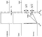
返回参考图1和图2,在实际应用中输入线电压152常常在90V~264V的范围中变化。由于非理想因素,诸如传输延迟,实际输出电流158不同于所设计的理想电流值,例如相差ΔIout的量。Referring back to FIGS. 1 and 2 , in practical applications the
图12是示出初级电流162的实际峰值大小与作为输入线电压152的函数的所希望峰值大小之差的系统100的简化时序图。波形1202表示作为时间的函数的信号226,波形1204表示作为时间的函数的信号156,波形1206表示作为时间的函数的、高输入线电压下的初级电流162,并且波形1208表示作为时间的函数的、低输入线电压下的初级电流162。FIG. 12 is a simplified timing diagram of the
如图12所示,在一开关时间周期期间,调制组件206在t0处将信号226从逻辑低电平变为逻辑高电平(例如,如波形1202所示),并且驱动组件210将信号156从逻辑低电平变为逻辑高电平(例如,如波形1204所示)。然后,在t1处,调制组件206将信号226从逻辑高电平变为逻辑低电平(例如,如波形1202所示)。在一传输延迟(例如Td)之后,驱动组件210将信号156从逻辑高电平变为逻辑低电平(例如,如波形1204所示的t2处)。在t0与t2之间,初级电流162的大小增大,例如,如波形1206和1208所示。与高的线输入电压相关联的初级电流比与低的线输入电压相关联的初级电流增大得更快,例如如波形1206和1208所示。初级电流162在t1与t2之间的增大可根据下式来确定:As shown in FIG. 12, during a switching time period,
其中,VAC表示输入线电压152,L表示初级绕组112的电感,并且Td表示传输延迟。电流感测信号164在t1与t2之间的与初级电流162的增大相对应的增大可根据下式来确定:where VAC represents the
其中,R5表示电流感测电阻器130的电阻。Wherein, R5 represents the resistance of the
根据式5,在相同的传输延迟下,与高的线输入电压相关联的初级电流162在t1与t2之间的改变在大小上大于与低的线输入电压相关联的其改变。因此,输出电流的残余量随着线输入电压而改变。According to Equation 5, the change in primary current 162 between t1 and t2 associated with a high line input voltage is larger in magnitude than its change associated with a low line input voltage for the same propagation delay. Therefore, the residual amount of output current varies with the line input voltage.
图13是示出根据本发明另一实施例的系统400的某些组件的简化示图。该示图仅仅是示例,其不应当不当地限制权利要求的范围。本领域技术人员将认识到许多变体、替换和修改。控制器402还包括晶体管1304,1306和1308以及运算放大器1310。例如,线电压补偿组件550包括电阻器424,430和432、晶体管1304,1306和1308、以及运算放大器1310。在另一示例中,线电压补偿组件650包括电阻器424,430和432、晶体管1304,1306和1308、以及运算放大器1310。FIG. 13 is a simplified diagram illustrating certain components of a
根据一个实施例,放大器1310的非反向输入端子(例如,如图13所示的“+”端子)被连接到地电压,并且放大器1310的反向输入端子(例如,如图13所示的“-”端子)被连接到端子440(例如,端子FB)。例如,在退磁过程之前和/或之后,如果开关428闭合(例如,接通),则辅助绕组416处的电压1318低于地电压(例如0V)。在另一示例中,运算放大器1310与晶体管1308一起工作来将端子440(例如,端子FB)处的电压1398调节为近似等于地电压(例如0V)。在又一示例中,电流1316经由端子440(例如,端子FB)通过电阻器424流出控制器402。在另一示例中,电流1316根据下式确定:According to one embodiment, the non-inverting input terminal of the amplifier 1310 (eg, the "+" terminal as shown in FIG. 13 ) is connected to ground voltage, and the inverting input terminal of the amplifier 1310 (eg, the "-" terminal) is connected to a terminal 440 (eg, terminal FB). For example, if the
其中,IFB表示电流1316,VAC表示线输入电压452,Nap表示辅助绕组416与初级绕组412之间的匝数比,并且R6表示电阻器424的电阻。在又一示例中,在退磁过程期间,如果辅助绕组416处的电压1318高于地电压,则端子440(例如,端子FB)处的电压1398高于地电压,并且作为响应,运算放大器1310输出信号1396以使晶体管1308截止。where IFB represents the current 1316 , VAC represents the line input voltage 452 , Nap represents the turns ratio between the auxiliary winding 416 and the primary winding 412 , and R6 represents the resistance of the
根据另一实施例,晶体管1304的大小(例如宽度与长度之比)与晶体管1306的大小成比例。例如,包括晶体管1304和1306的电流镜电路对电流1316进行镜像以生成电流1314。在另一示例中,电流1314从晶体管1306通过端子444(例如,端子CS)流到电阻器432。在又一示例中,退磁过程之前和/或之后的电流1314根据下式确定:According to another embodiment, the size (eg width to length ratio) of
其中,ICC_AC表示电流1314,并且s表示晶体管1304的大小与晶体管1306的大小之比。在另一示例中,退磁过程之前和/或之后的对于电流感测信号1320的补偿值根据下式确定:where ICC_AC represents the current 1314 and s represents the ratio of the size of
其中,ΔCS表示对于电流感测信号1320的补偿值,并且R4表示电阻器432的电阻。例如,端子444处的电压在大小上等于电流感测信号1320被提高ΔCS。在另一示例中,电流感测信号1320的大小与初级电流462成比例。Wherein, ΔCS represents the compensation value for the
在一个实施例中,如果将某个误差输出电流考虑在内而不考虑对于电流感测信号1320的任何补偿(例如,如式9所示的ΔCS),则系统400的平均输出电流根据下式确定:In one embodiment, the average output current of the
其中,N表示初级绕组412与次级绕组414之间的匝数比,Vref_ea表示内部参考信号(例如参考信号522或参考信号622),Rcs表示电阻器430的电阻,并且ΔIo(VAC)表示作为线输入电压452(例如VAC)的函数的误差输出电流。where N represents the turns ratio between primary winding 412 and secondary winding 414, Vref_ea represents an internal reference signal (such as
在另一实施例中,如果对于电流感测信号1320的补偿(例如,如式9所示的ΔCS)也被考虑在内,则内部参考信号(例如参考信号522或参考信号622)被有效地减小与补偿相同的量。例如,基于式10,获得下式:In another embodiment, if the compensation for the current sense signal 1320 (eg, ΔCS as shown in Equation 9) is also taken into account, the internal reference signal (eg,
因此,根据某些实施例,在不同的输入线电压下,可通过调节对于电流感测信号1320的补偿值ΔCS(例如,通过调节电阻器432和424的电阻)来使系统400的平均输出电流保持近似恒定。Therefore, according to some embodiments, at different input line voltages, the average output current of the
返回参考图1和图2,通常,由于变压器110的漏电感,初级侧中的能量不能被完全传送到次级侧,因此,输出电流158与所设计的理想电流值例如相差ΔIout的量。该差值随着输出电压168改变。Referring back to FIGS. 1 and 2 , typically, the energy in the primary side cannot be fully transferred to the secondary side due to the leakage inductance of the transformer 110 , and therefore, the output current 158 differs from the designed ideal current value by, for example, ΔIout . This difference varies with
图14是示出作为输出电压168的函数的次级电流169的峰值大小的系统100的简化时序图。波形1402表示作为时间的函数的初级电流162,并且波形1404表示作为时间的函数的次级电流169。例如,次级电流169与输出电流158紧密相关。FIG. 14 is a simplified timing diagram of the
如图14所示,在接通时间段期间(例如,t5与t6之间),开关128闭合(例如接通),并且初级电流162的大小增大,例如如波形1402所示。在t6,开关128断开(例如关断)。在时间段Δt期间(例如,t6与t7之间),初级电流162的大小由于漏电感而减小(例如如波形1402所示),并且次级电流169的大小从低的大小(例如,t6)增大到峰值大小(例如,t7处),如波形1404所示。在t7之后,次级电流169的大小减小,例如如波形1404所示。如果输出电压168的大小增大,则时间段Δt(例如,t6与t7之间)的持续时间增大并且次级电流169的峰值大小减小(例如如波形1404所示)。因此,输出电流158的大小减小,并且输出电流158与理想电流值之差增大。As shown in FIG. 14 , during the on-time period (eg, betweent5 andt6 ),
图15是示出根据本发明又一实施例的系统400的某些组件的简化示图。该示图仅仅是示例,其不应当不当地限制权利要求的范围。本领域技术人员将认识到许多变体、替换和修改。控制器402还包括晶体管1504,1506,1510,1518和1520、运算放大器1508、电阻器1516、电容器1512以及开关1514。例如,负载补偿组件560包括电阻器432、晶体管1504,1506,1510,1518和1520、运算放大器1508、电阻器1516、电容器1512和开关1514。在另一示例中,负载补偿组件660包括电阻器432、晶体管1504,1506,1510,1518和1520、运算放大器1508、电阻器1516、电容器1512和开关1514。FIG. 15 is a simplified diagram illustrating certain components of a
根据一个实施例,如果在次级绕组414的退磁过程期间开关1514响应于采样信号1538而闭合(例如接通),则反馈信号460被采样并被保持在电容器1512处。例如,放大器1508在非反向输入端子(例如,如图15所示的“+”端子)处接收采样和保持信号1530。在另一示例中,采样和保持信号1530根据下式确定:According to one embodiment, if
VFB_sample=Vout×Nas (式13)VFB_sample = Vout ×Nas (Formula 13)
其中,VFB_sample表示采样和保持信号1530,Vout表示输出电压468,并且Nas表示辅助绕组416与次级绕组414之间的匝数比。在又一示例中,在次级绕组414的退磁过程之前和/或之后,开关1514响应于采样信号1538而断开(例如关断)。在又一示例中,采样信号1538与信号538相同。在又一示例中,采样信号1538与信号638相同。Where VFB_sample represents the sample and hold
根据另一实施例,如果开关428在接通时间段期间闭合(例如接通),则电流1522流经晶体管1504和1510以及电阻器1516。例如,包括晶体管1504,1506,1518和1520的电流镜电路对电流1522进行镜像以生成流经晶体管1506和1518的电流1524,并且对电流1524镜像以生成补偿电流1526(例如,ICC_load)。在另一示例中,补偿电流1526从电阻器432通过端子444流到晶体管1520。在又一示例中,在退磁过程期间,补偿电流1526根据下式确定:According to another embodiment, current 1522 flows through
其中,ICC_load表示电流1526,VFB_sample表示采样和保持信号1530,R151表示电阻器1516的电阻,并且p表示与包括晶体管1504,1506,1518和1520在内的电流镜电路相关联的比率。在又一示例中,电流1526流经电阻器432以提供对电流感测信号1532的补偿值,该补偿值在退磁过程期间可根据下式确定:where ICC_load represents current 1526 , VFB_sample represents sample and hold
其中,ΔCS’表示对电流感测信号1532的补偿值,并且R4表示电阻器432的电阻。例如,端子444处的电压在大小上等于电流感测信号1532降低ΔCS’。在另一示例中,电流感测信号1532在大小上与初级电流462成比例。Wherein, ΔCS' represents the compensation value for the
在一个实施例中,如果考虑到某个误差输出电流而不考虑对电流感测信号1532的补偿(例如,如式15所示的ΔCS’),则系统400的平均输出电流根据下式确定:In one embodiment, the average output current of the
其中,N表示初级绕组412与次级绕组414之间的匝数比,Vref_ea表示内部参考信号(例如,参考信号522或参考信号622),Rcs表示电阻器430的电阻,并且ΔIo(Vout)表示作为输出电压468(例如Vout)的函数的误差电流。where N represents the turns ratio between primary winding 412 and secondary winding 414, Vref_ea represents an internal reference signal (eg,
在另一实施例中,如果对电流感测信号1532的补偿(例如,如式15所示的ΔCS’)也被考虑在内,则内部参考信号(例如,参考信号522或参考信号622)被有效地减少与补偿相同的量。例如,基于式16,下式被获得:In another embodiment, if the compensation for the current sense signal 1532 (eg, ΔCS' as shown in Equation 15) is also taken into account, the internal reference signal (eg,
因此,根据某些实施例,在不同的输出电压下,可通过调节对于电流感测信号1532的补偿值ΔCS’(例如,通过调节电阻器432和1516的电阻)来使系统400的平均输出电流保持近似恒定。Therefore, according to some embodiments, at different output voltages, the average output current of the
图16是示出根据本发明又一实施例的系统400的某些组件的简化示图。该示图仅仅是示例,其不应当不当地限制权利要求的范围。本领域技术人员将认识到许多变体、替换和修改。控制器402还包括晶体管1604,1606,1618和1620、跨导放大器1608、电容器1612和开关1614。例如,负载补偿组件560包括电阻器432、晶体管1604,1606,1618和1620、跨导放大器1608、电容器1612和开关1614。在另一示例中,负载补偿组件660包括电阻器432、晶体管1604,1606,1618和1620、跨导放大器1608、电容器1612和开关1614。FIG. 16 is a simplified diagram illustrating certain components of a
根据一个实施例,如果在次级绕组414的退磁过程期间开关1614响应于采样信号1638而闭合(例如,接通),则反馈信号460被采样并被保持在电容器1612处。例如,跨导放大器1608在反向输入端子(例如,图16所示的“-”端子)处接收采样和保持信号1630并且在非反向输入端子(例如,如图16所示的“+”端子)处接收阈值信号1610(例如,Vth_load)并且生成电流1622(例如,Igm)。在另一示例中,采样和保持信号1630根据下式确定:According to one embodiment, if
VFB_sample=Vout×Nas (式18)VFB_sample = Vout × Nas (Formula 18)
其中,VFB_sample表示采样和保持信号1630,Vout表示输出电压468,并且Nas表示辅助绕组416与次级绕组414之间的匝数比。在又一示例中,在次级绕组414的退磁过程之前和/或之后,开关1614响应于采样信号1638而断开(例如关断)。在又一示例中,采样信号1638与信号538相同。在又一示例中,采样信号1638与信号638相同。Where VFB_sample represents the sample and hold
根据另一实施例,包括晶体管1504、1506、1518和1520的电流镜电路对电流1622进行镜像以生成流经晶体管1604和1620的电流1624,并且对电流1624进行镜像以生成补偿电流1626(例如,Icc_load)。例如,补偿电流1626从晶体管1606通过端子444流到电阻器432。在另一示例中,在退磁过程期间,补偿电流1626根据下式确定:According to another embodiment, a current mirror
其中,ICC_load表示电流1626,VFB_sample表示采样和保持信号1630,gm表示放大器1608的跨导,并且p表示与包括晶体管1604,1606,1618和1620的电流镜电路相关联的比率。在另一示例中,补偿电流1626(例如Icc_load)流经电阻器432以提供对电流感测信号1632的补偿值,该补偿值在退磁过程期间可根据下式确定:where ICC_load represents current 1626 , VFB_sample represents sample and hold
其中,ΔCS”表示对电流感测信号1632的补偿值,并且R4表示电阻器432的电阻。例如,端子444处的电压在大小上等于电流感测信号1632降低ΔCS”。在另一示例中,电流感测信号1632在大小上与初级电流462成比例。Where ΔCS" represents the compensation value for the
在一个实施例中,如果考虑某个误差输出电流但不考虑对电流感测信号1632的补偿(例如,如式20所示的ΔCS”),则根据下式确定系统400的平均输出电流:In one embodiment, if a certain error output current is considered but no compensation for the current sense signal 1632 (e.g., ΔCS" as shown in Equation 20), the average output current of the
其中N表示初级绕组412与次级绕组414之间的匝数比,Vref_ea表示内部参考信号(例如参考信号522或参考信号622),Rcs表示电阻器430的电阻,并且ΔIo(Vout)表示作为输出电压468(例如Vout)的函数的误差电流。where N represents the turns ratio between primary winding 412 and secondary winding 414, Vref_ea represents an internal reference signal (eg,
在另一实施例中,如果对电流感测信号1632的补偿(例如,如式20所示的ΔCS”)也被考虑在内,则内部参考信号(例如参考信号522或参考信号622)被有效地减小与补偿相同的量。例如,基于式21,获得下式:In another embodiment, an internal reference signal (eg,
因此,根据某些实施例,在不同的输出电压下,可通过调节对于电流感测信号1632的补偿值ΔCS”(例如,通过调节电阻器432的电阻)来使系统400的平均输出电流保持近似恒定。Therefore, according to some embodiments, at different output voltages, the average output current of
图17是示出根据本发明又一实施例的作为电源变换系统400一部分的控制器402的简化示图。该示图仅仅是示例,其不应当不当地限制权利要求的范围。本领域技术人员将认识到许多变体、替换和修改。FIG. 17 is a simplified diagram illustrating a
控制器402包括振荡器1702、欠压锁定(UVLO)组件1704、调制组件1706、逻辑控制器1708、驱动组件1710、退磁检测器1712、误差放大器1716、电流感测组件1714和斩波组件1740。另外,控制器402包括线电压补偿组件1750的至少一部分和负载补偿组件1760的至少一部分。例如,误差放大器1716与误差放大器516相同。在另一示例中,线电压补偿组件1750与线电压补偿组件550相同。在又一示例中,负载补偿组件1760与负载补偿组件560相同。
根据一个实施例,UVLO组件1704检测信号454并输出信号1718。例如,如果信号454的大小大于预定阈值,则控制器402开始正常工作。在另一示例中,如果信号454的大小小于该预定阈值,则控制器402关断。在又一示例中,误差放大器1716接收参考信号1722和来自电流感测组件1714的信号1720,并且向调制组件1706输出放大信号1724。在又一示例中,调制组件1706还接收来自振荡器1702的信号1728并且输出调制信号1726。在又一示例中,信号1728是斜坡信号并且在每个开关时间周期期间线性地或非线性地增大到峰值大小。在又一示例中,调制信号1726是具有固定开关频率的脉宽调制(PWM)信号并且信号1726的占空比基于信号1724与信号1728之间的比较来确定。在又一示例中,逻辑控制器1708处理调制信号1726并且向驱动组件1710输出控制信号1730,驱动组件1710生成信号456以接通或关断开关428。在又一示例中,逻辑控制器1708还输出控制信号1730给电流感测组件1714。According to one embodiment,
根据另一实施例,如果控制信号1730为逻辑高电平,控制信号456为逻辑高电平。例如,如果控制信号1730为逻辑低电平,则控制信号456为逻辑低电平。在另一示例中,退磁检测器1712检测反馈信号460并且输出退磁信号1732以用于确定每个开关时间周期期间次级绕组414的退磁过程的开始和结束。在又一示例中,退磁信号1732在每个开关周期的退磁时段期间为逻辑高电平,并且在每个开关周期的其余时段期间为逻辑低电平。在又一示例中,如果控制信号456从逻辑高电平变为逻辑低电平,则退磁信号1732从逻辑低电平变为逻辑高电平。在又一示例中,退磁检测器1712向负载补偿组件1760输出采样信号1738,负载补偿组件1760输出补偿信号1798以影响误差放大器1716的输出。According to another embodiment, if the
根据又一实施例,斩波组件1740接收来自振荡器1702的时钟信号1734并且向误差放大器1716输出信号1736。例如,信号1736也是时钟信号,其具有50%的占空比且其频率是时钟信号1734的频率的1/N。在另一示例中,信号1736用于对误差放大器1716进行斩波。在又一示例中,线电压补偿组件1750用于在宽范围的输入线电压下使输出电流保持近似恒定(例如,具有小的误差)。在又一示例中,负载补偿组件1760用于在宽范围的输出电压下使输出电流保持近似恒定(例如,具有小的误差)。According to yet another embodiment, the
如上面讨论且在此进一步强调的,图17仅仅是示例,其不应当不当地限制权利要求的范围。本领域技术人员将认识到许多变体、替换和修改。例如,电流感测组件1714与电流感测组件214相同。在另一示例中,误差放大器1716可由误差放大器216替代。在一些实施例中,线电压补偿组件1750被去除。在某些实施例中,负载补偿组件1760被去除。As discussed above and further emphasized here, FIG. 17 is an example only, which should not unduly limit the scope of the claims. Those skilled in the art will recognize many variations, substitutions and modifications. For example,
图18是示出根据本发明又一实施例的作为电源变换系统400一部分的控制器402的简化示图。该示图仅仅是示例,其不应当不当地限制权利要求的范围。本领域技术人员将认识到许多变体、替换和修改。FIG. 18 is a simplified diagram illustrating a
控制器402包括斜坡信号生成器2002、欠压锁定(UVLO)组件2004、调制组件2006、逻辑控制器2008、驱动组件2010、退磁检测器2012、误差放大器2016、电流感测组件2014和斩波组件2040。另外,控制器402包括线电压补偿组件2050的至少一部分和负载补偿组件2060的至少一部分。例如,误差放大器2016与误差放大器616相同。在另一示例中,线电压补偿组件2050与线电压补偿组件650相同。在又一示例中,负载补偿组件2060与负载补偿组件660相同。The
根据一个实施例,UVLO组件2004检测信号454并且输出信号2018。例如,如果信号454的大小大于预定阈值,则控制器402开始正常工作。在另一示例中,如果信号454的大小小于预定阈值,则控制器402关断。在又一示例中,误差放大器2016接收参考信号2022和来自电流感测组件2014的信号2020,并且向调制组件2006输出放大信号2024。在又一示例中,调制组件2006还接收来自振荡器2002的信号2028并且输出调制信号2026。在又一示例中,信号2028是斜坡信号并且在每个开关时间周期期间线性地或非线性地增大到峰值大小。在又一示例中,调制信号2026不具有固定开关频率。在又一示例中,逻辑控制器2008处理调制信号2026并且向驱动组件2010输出控制信号2030,驱动组件2010生成信号456以接通或关断开关428。在又一示例中,逻辑控制器2008还向电流感测组件2014输出控制信号2030。According to one embodiment, UVLO component 2004 detects signal 454 and outputs signal 2018 . For example, if the magnitude of the
根据另一实施例,如果控制信号2030为逻辑高电平,则控制信号456为逻辑高电平。例如,如果控制信号2030为逻辑低电平,则控制信号456为逻辑低电平。在另一示例中,退磁检测器2012检测反馈信号2060并且输出退磁信号2032以用于确定每个开关时间周期期间次级绕组414的退磁过程的开始和结束。在又一示例中,退磁信号2032在每个开关周期的退磁时段期间为逻辑高电平,并且在每个开关周期的其余时段期间为逻辑低电平。在又一示例中,如果控制信号456从逻辑高电平变为逻辑低电平,则退磁信号2032从逻辑低电平变为逻辑高电平。在又一示例中,退磁检测器2012向负载补偿组件2060输出采样信号2038,负载补偿组件2060输出补偿信号2098以影响误差放大器2016的输出。在又一示例中,斜坡信号生成器2002接收控制信号2030并向调制组件2006输出信号2028。According to another embodiment, if the
根据又一实施例,斩波组件2040接收来自逻辑控制器2008的控制信号2030并且向误差放大器2016输出信号2036。例如,信号2036也是时钟信号,其具有50%的占空比且其频率是控制信号2030的频率的1/N。在另一示例中,信号2036用于对误差放大器2016进行斩波。在又一示例中,线电压补偿组件2050用于在宽范围的输入线电压内保持恒定输出电流的精度。在又一示例中,负载补偿组件2060用于在宽范围的输出电压内保持恒定输出电流的精度。According to yet another embodiment, the
如上面讨论且在此进一步强调的,图18仅仅是示例,其不应当不当地限制权利要求的范围。本领域技术人员将认识到许多变体、替换和修改。例如,电流感测组件2014与电流感测组件214相同。在另一示例中,误差放大器2016可由误差放大器216替代。在一些实施例中,线电压补偿组件2050被去除。在某些实施例中,负载补偿组件2060被去除。As discussed above and further emphasized here, FIG. 18 is an example only, which should not unduly limit the scope of the claims. Those skilled in the art will recognize many variations, substitutions and modifications. For example,
图19是根据本发明又一实施例的系统400的某些组件的简化示图。该示图仅仅是示例,其不应当不当地限制权利要求的范围。本领域技术人员将认识到许多变体、替换和修改。FIG. 19 is a simplified diagram of certain components of a
控制器402包括负载补偿组件1960、电流感测组件1914和误差放大器1916。负载补偿组件1960包括晶体管1818和1820、跨导放大器1808、电容器1812和开关1814。例如,负载补偿组件1960与负载补偿组件1760相同。在另一示例中,负载补偿组件1960与负载补偿组件2060相同。在又一示例中,电流感测组件1914与电流感测组件1714相同。在又一示例中,电流感测组件1914与电流感测组件2014相同。在又一示例中,误差放大器1916与误差放大器1716相同。在又一示例中,误差放大器1916与误差放大器2016相同。
根据一个实施例,误差放大器1916的输出电流1924与由电流感测组件1914生成的输出信号1920和参考信号1922之差有关。例如,误差放大器1916的输出电流1924在大小上与参考信号1922和输出信号1920之差成比例。According to one embodiment, the
根据另一实施例,如果在次级绕组414的退磁过程期间开关1814响应于采样信号1938而闭合(例如接通),则反馈信号460被采样并被保持在电容器1812处。例如,跨导放大器1808在反向输入端子(例如,如图19所示的“-”端子)处接收采样和保持信号1830并且在非反向输入端子(例如,如图19所示的“+”端子)处接收阈值信号1810(例如,Vth_load),并且生成电流1822(例如,Igm)。在另一示例中,采样和保持信号1830根据下式确定:According to another embodiment, if switch 1814 is closed (eg, turned on) in response to
VFB_sample=Vout×Nas (式23)VFB_sample = Vout × Nas (Formula 23)
其中,VFB_sample表示采样和保持信号1830,Vout表示输出电压468,并且Nas表示辅助绕组416与次级绕组414之间的匝数比。在又一示例中,在次级绕组414的退磁过程之前和/或之后,开关1814响应于采样信号1938而断开(例如关断)。在又一示例中,采样信号1938与信号1738相同。在又一示例中,采样信号1938与信号2038相同。Where VFB_sample represents the sample and hold
根据又一实施例,包括晶体管1818和1820的电流镜电路对电流1822进行镜像以生成补偿电流1824(例如Icc_load)。例如,该电流镜电路在电路节点1930处被耦合到误差放大器1916,并且输出电流1924被划分为补偿电流1824和电流1926。在一个实施例中,输出电流1924从误差放大器1916流到电路节点1930,补偿电流从电路节点1930流到晶体管1820,并且电流1926从电路节点1930流到端子448。在另一实施例中,电流1926在大小上等于输出电流1924减去补偿电流1824。According to yet another embodiment, a current mirror
根据又一实施例,在退磁过程期间,补偿电流1824根据下式确定:According to yet another embodiment, during the demagnetization process, the compensation current 1824 is determined according to the following equation:
其中,ICC_load表示电流1824,VFB_sample表示采样和保持信号1830,gm表示放大器1808的跨导,并且p表示与包括晶体管1818和1820的电流镜电路相关联的比率。例如,在退磁过程期间补偿电流1824(例如Icc_load)对误差放大器1916的影响近似等效于生成参考信号1922(例如Vref_ea)的补偿值。在另一示例中,参考信号1922的补偿值根据下式确定:where ICC_load represents current 1824 , VFB_sample represents sample and hold
其中,ΔVref_ea表示对参考信号1922的补偿值,并且gm_ea表示误差放大器1916的跨导。where ΔVref_ea represents the compensation value for the
在一个实施例中,如果考虑某个误差输出电流但不考虑对参考信号1922(例如Vref_ea)的补偿(例如,如式25所示的ΔVref_ea),则根据下式确定系统400的平均输出电流:In oneembodiment , the averageoutput of the
其中N表示初级绕组412与次级绕组414之间的匝数比,Vref_ea表示参考信号1922,Rcs表示电阻器430的电阻,并且ΔIo(Vout)表示作为输出电压468(例如Vout)的函数的误差电流。where N represents the turns ratio between the primary winding 412 and the secondary winding 414, Vref_ea represents the
在另一实施例中,如果对参考信号1922(例如Vref_ea)的补偿(例如,如式25所示的ΔVref_ea)也被考虑在内,则则根据下式确定系统400的平均输出电流:In another embodiment, if the compensation (eg, ΔVref_ea as shown in Equation 25) to the reference signal 1922 (eg, Vref_ea ) is also taken into account, then the average output current of the
因此,根据某些实施例,在不同的输出电压下,可通过调节对于参考信号1922(例如Vref_ea)的补偿(例如,ΔVref_ea)(例如,通过调节电阻器424的电阻与电阻器426的电阻之间的比率)来使系统400的平均输出电流保持近似恒定。Therefore, according to some embodiments, at different output voltages, the compensation (eg, ΔVref_ea ) for the reference signal 1922 (eg, Vref_ea ) can be adjusted (eg, by adjusting the resistance of
根据另一实施例,一种用于处理与电源变换系统的电流相关联的输入信号和参考信号的误差放大器包括:第一运算放大器、第二运算放大器、第一晶体管、第二晶体管、电流镜组件、开关、第一电阻器和第二电阻器。第一运算放大器包括第一输入端子、第二输入端子和第一输出端子,所述第一输入端子被配置为接收参考信号。第一晶体管包括第一晶体管端子、第二晶体管端子和第三晶体管端子,所述第一晶体管端子被配置为从所述第一输出端子接收第一放大信号,所述第三晶体管端子被耦合到所述第二输入端子。第二运算放大器包括第三输入端子、第四输入端子和第二输出端子,所述第三输入端子被配置为接收与流经电源变换系统的初级绕组的电流相关联的输入信号。第二晶体管包括第四晶体管端子、第五晶体管端子和第六晶体管端子,所述第四晶体管端子被配置为从所述第二输出端子接收第二放大信号,所述第六晶体管端子被耦合到所述第四输入端子。电流镜组件包括第一组件端子和第二组件端子,所述第一组件端子被耦合到所述第二晶体管端子。开关包括第一开关端子和第二开关端子,所述第一开关端子被耦合到所述第二组件端子,所述第二开关端子被耦合到所述第五晶体管端子。第一电阻器包括第一电阻器端子和第二电阻器端子,所述第一电阻器与第一电阻相关联,所述第一电阻器端子被耦合到所述第二输入端子。第二电阻器包括第三电阻器端子和第四电阻器端子,所述第二电阻器与第二电阻相关联,所述第三电阻器端子被耦合到所述第四输入端子。所述第一电阻的大小大于所述第二电阻。所述第二组件端子被配置为至少基于与所述参考信号和所述输入信号相关联的信息输出输出信号。例如,该误差放大器至少根据图7、图8、图9、图10和/或图11来实现。According to another embodiment, an error amplifier for processing an input signal and a reference signal associated with a current of a power conversion system includes: a first operational amplifier, a second operational amplifier, a first transistor, a second transistor, a current mirror components, switch, first resistor and second resistor. The first operational amplifier includes a first input terminal, a second input terminal and a first output terminal, the first input terminal being configured to receive a reference signal. The first transistor includes a first transistor terminal configured to receive a first amplified signal from the first output terminal, a second transistor terminal and a third transistor terminal, the third transistor terminal being coupled to the second input terminal. The second operational amplifier includes a third input terminal, a fourth input terminal, and a second output terminal, the third input terminal being configured to receive an input signal associated with current flowing through the primary winding of the power conversion system. The second transistor includes a fourth transistor terminal, a fifth transistor terminal and a sixth transistor terminal, the fourth transistor terminal being configured to receive a second amplified signal from the second output terminal, the sixth transistor terminal being coupled to the fourth input terminal. A current mirror component includes a first component terminal and a second component terminal, the first component terminal being coupled to the second transistor terminal. A switch includes a first switch terminal coupled to the second component terminal and a second switch terminal coupled to the fifth transistor terminal. The first resistor includes a first resistor terminal and a second resistor terminal, the first resistor being associated with the first resistance, the first resistor terminal being coupled to the second input terminal. The second resistor includes a third resistor terminal and a fourth resistor terminal, the second resistor being associated with the second resistance, the third resistor terminal being coupled to the fourth input terminal. The magnitude of the first resistor is greater than that of the second resistor. The second component terminal is configured to output an output signal based at least on information associated with the reference signal and the input signal. For example, the error amplifier is implemented at least according to FIGS. 7 , 8 , 9 , 10 and/or 11 .
根据另一实施例,一种用于调整电源变换系统的系统控制器包括:第一控制器端子,被配置为接收与第一电流相关联的第一电压,所述第一电流与电源变换系统的输入电压有关;补偿组件,被耦合到所述第一控制器端子并被配置为如果所述第一电压满足一个或多个第一条件则至少基于与所述第一电流相关联的信息生成补偿电流;以及第二控制器端子,被耦合到所述补偿组件并被配置为至少基于与所述补偿电流相关联的信息提供补偿电压,所述补偿电压的大小等于所述补偿电流乘以补偿电阻,所述补偿电阻与补偿电阻器相关联。该系统控制器还包括:电流感测组件,被配置为接收第二电压并且生成第二输出信号,所述第二电压的大小等于第三电压与所述补偿电压之和,所述第三电压与流经所述电源变换系统的初级绕组的第二电流成比例;以及误差放大器,被配置为接收所述输出信号和参考信号,至少基于与所述输出信号和所述参考信号相关联的信息生成放大信号,并且输出所述放大信号以影响与所述第二电流相关联的开关。例如,该系统控制器至少根据图13来实现。According to another embodiment, a system controller for regulating a power conversion system includes: a first controller terminal configured to receive a first voltage associated with a first current, the first current being related to a power conversion system related to the input voltage; a compensation component coupled to the first controller terminal and configured to generate, based at least on information associated with the first current, if the first voltage satisfies one or more first conditions a compensation current; and a second controller terminal coupled to the compensation component and configured to provide a compensation voltage having a magnitude equal to the compensation current multiplied by a compensation current based at least on information associated with the compensation current A resistor, the compensation resistor is associated with the compensation resistor. The system controller further includes: a current sensing component configured to receive a second voltage equal to a sum of a third voltage and the compensation voltage, and generate a second output signal, the third voltage proportional to a second current flowing through a primary winding of the power conversion system; and an error amplifier configured to receive the output signal and a reference signal based at least on information associated with the output signal and the reference signal An amplified signal is generated and output to affect a switch associated with the second current. For example, the system controller is implemented according to at least FIG. 13 .
根据又一实施例,一种用于调整电源变换系统的系统控制器包括:第一控制器端子,被配置为接收与电源变换系统的输出电压相关联的反馈信号;补偿组件,被耦合到所述第一控制器端子并被配置为在所述电源变换系统的退磁过程期间对所述反馈信号采样并且至少基于与所述第一电流相关联的信息生成补偿电流;以及第二控制器端子,被耦合到所述补偿组件并被配置为至少基于与所述补偿电流相关联的信息提供补偿电压,所述补偿电压的大小等于所述补偿电流乘以补偿电阻,所述补偿电阻与补偿电阻器相关联。另外,该系统控制器包括:电流感测组件,被配置为接收输入电压并且生成输出信号,所述输入电压的大小等于第一电压与所述补偿电压之和,所述第一电压与流经所述电源变换系统的初级绕组的第一电流成比例;以及误差放大器,被配置为接收所述输出信号和参考信号,至少基于与所述输出信号和所述参考信号相关联的信息生成放大信号,并且输出所述放大信号以影响与所述第一电流相关联的开关。例如,该系统控制器至少根据图15和/或图16来实现。According to yet another embodiment, a system controller for regulating a power conversion system includes: a first controller terminal configured to receive a feedback signal associated with an output voltage of the power conversion system; a compensation component coupled to the the first controller terminal and configured to sample the feedback signal and generate a compensation current based at least on information associated with the first current during a demagnetization process of the power conversion system; and a second controller terminal, coupled to the compensation component and configured to provide a compensation voltage equal to the compensation current multiplied by a compensation resistance based at least on information associated with the compensation current, the compensation resistance being equal to the compensation resistor Associated. In addition, the system controller includes: a current sensing component configured to receive an input voltage equal to the sum of a first voltage and the compensation voltage, the first voltage and the current flowing through it and generate an output signal. a first current proportional to a primary winding of the power conversion system; and an error amplifier configured to receive the output signal and a reference signal, generate an amplified signal based at least on information associated with the output signal and the reference signal , and outputting the amplified signal to affect a switch associated with the first current. For example, the system controller is implemented according to at least FIG. 15 and/or FIG. 16 .
根据又一实施例,一种用于调整电源变换系统的系统控制器包括:第一控制器端子,被配置为接收与电源变换系统的输出电压相关联的反馈信号;补偿组件,被耦合到所述第一控制器端子并被配置为在所述电源变换系统的退磁过程期间对所述反馈信号采样并且至少基于与被采样的反馈信号相关联的信息生成补偿电流;以及误差放大器,包括第一输入端子、第二输入端子和被耦合到所述补偿组件的输出端子。所述第一输入端子被配置为接收输入电压,所述第二输入端子被配置为接收参考电压,并且所述输出端子被配置为输出在大小上与所述输入电压和所述参考电压之差相关的第一输出电流。所述误差放大器和所述补偿组件还被配置为生成在大小上与所述第一输出电流和所述补偿电流之差相等的第二输出电流。例如,该系统控制器至少根据图19来实现。According to yet another embodiment, a system controller for regulating a power conversion system includes: a first controller terminal configured to receive a feedback signal associated with an output voltage of the power conversion system; a compensation component coupled to the the first controller terminal and configured to sample the feedback signal during a demagnetization process of the power conversion system and generate a compensation current based at least on information associated with the sampled feedback signal; and an error amplifier comprising a first An input terminal, a second input terminal and an output terminal coupled to the compensation component. The first input terminal is configured to receive an input voltage, the second input terminal is configured to receive a reference voltage, and the output terminal is configured to output a difference in magnitude to the input voltage and the reference voltage related to the first output current. The error amplifier and the compensation component are further configured to generate a second output current equal in magnitude to a difference between the first output current and the compensation current. For example, the system controller is implemented according to at least FIG. 19 .
在一个实施例中,一种用于调整电源变换系统的方法包括:接收与第一电流相关联的第一电压,所述第一电流与电源变换系统的输入电压有关;如果所述第一电压满足一个或多个第一条件,则至少基于与所述第一电流相关联的信息生成补偿电流;以及至少基于与所述补偿电流相关联的信息提供补偿电压,所述补偿电压的大小等于所述补偿电流乘以补偿电阻,所述补偿电阻与补偿电阻器相关联。该方法还包括:接收输入电压,所述输入电压的大小等于第二电压与所述补偿电压之和,所述第二电压与流经所述电源变换系统的初级绕组的第二电流成比例;至少基于与所述输入电压相关联的信息生成输出信号;以及接收所述输出信号和参考信号。另外,该方法包括:至少基于与所述输出信号和所述参考信号相关联的信息生成放大信号;以及输出所述放大信号以影响与所述第二电流相关联的开关。例如,该方法至少根据图13来实现。In one embodiment, a method for regulating a power conversion system includes: receiving a first voltage associated with a first current, the first current being related to an input voltage of the power conversion system; if the first voltage If one or more first conditions are met, generating a compensation current based at least on information associated with the first current; and providing a compensation voltage at least based on information associated with the compensation current, the magnitude of the compensation voltage being equal to the The compensation current is multiplied by a compensation resistance associated with the compensation resistor. The method further includes: receiving an input voltage having a magnitude equal to a sum of a second voltage and the compensation voltage, the second voltage being proportional to a second current flowing through the primary winding of the power conversion system; generating an output signal based at least on information associated with the input voltage; and receiving the output signal and a reference signal. Additionally, the method includes: generating an amplified signal based at least on information associated with the output signal and the reference signal; and outputting the amplified signal to affect a switch associated with the second current. For example, the method is implemented according to at least FIG. 13 .
在另一实施例中,一种用于调整电源变换系统的方法包括:接收与电源变换系统的输出电压相关联的反馈信号;在所述电源变换系统的退磁过程期间对所述反馈信号采样;以及至少基于与被采样的反馈信号相关联的信息生成补偿电流。该方法还包括:至少基于与所述补偿电流相关联的信息提供补偿电压,所述补偿电压的大小等于所述补偿电流乘以补偿电阻,所述补偿电阻与补偿电阻器相关联;接收输入电压,所述输入电压的大小等于第一电压与所述补偿电压之和,所述第一电压与流经所述电源变换系统的初级绕组的第一电流成比例;以及生成输出信号。另外,该方法包括:接收所述输出信号和参考信号;至少基于与所述输出信号和所述参考信号相关联的信息生成放大信号;以及输出所述放大信号以影响与所述第一电流相关联的开关。例如,该方法至少根据图15和/或图16来实现。In another embodiment, a method for regulating a power conversion system includes: receiving a feedback signal associated with an output voltage of a power conversion system; sampling the feedback signal during a demagnetization process of the power conversion system; and generating a compensation current based at least on information associated with the sampled feedback signal. The method also includes providing a compensation voltage based at least on information associated with the compensation current, the compensation voltage having a magnitude equal to the compensation current multiplied by a compensation resistance associated with the compensation resistor; receiving an input voltage , the magnitude of the input voltage is equal to the sum of a first voltage and the compensation voltage, the first voltage is proportional to a first current flowing through the primary winding of the power conversion system; and an output signal is generated. Additionally, the method includes: receiving the output signal and a reference signal; generating an amplified signal based at least on information associated with the output signal and the reference signal; and outputting the amplified signal to affect linked switch. For example, the method is implemented according to at least FIG. 15 and/or FIG. 16 .
在又一实施例中,一种用于调整电源变换系统的方法包括:接收与电源变换系统的输出电压相关联的反馈信号;在所述电源变换系统的退磁过程期间对所述反馈信号采样;以及至少基于与被采样的反馈信号相关联的信息生成补偿电流。另外,该方法包括在误差放大器的第一输入端子处接收输入电压,所述误差放大器还包括第二输入端子和输出端子。此外,该方法包括:在所述第二输入端子处接收参考电压;在所述输出端子处生成在大小上与所述输入电压和所述参考电压之差相关的第一输出电流;以及输出在大小上与所述第一输出电流和所述补偿电流之差相等的第二输出电流。例如,该方法至少根据图19来实现。In yet another embodiment, a method for regulating a power conversion system includes: receiving a feedback signal associated with an output voltage of a power conversion system; sampling the feedback signal during a demagnetization process of the power conversion system; and generating a compensation current based at least on information associated with the sampled feedback signal. Additionally, the method includes receiving an input voltage at a first input terminal of an error amplifier, the error amplifier also including a second input terminal and an output terminal. Additionally, the method includes: receiving a reference voltage at the second input terminal; generating a first output current at the output terminal that is related in magnitude to the difference between the input voltage and the reference voltage; and outputting at the output terminal a second output current equal in magnitude to the difference between the first output current and the compensation current. For example, the method is implemented according to at least FIG. 19 .
例如,本发明各个实施例中的一些或所有组件单独地和/或与至少另一组件相组合地是利用一个或多个软件组件、一个或多个硬件组件和/或软件与硬件组件的一种或多种组合来实现的。在另一示例中,本发明各个实施例中的一些或所有组件单独地和/或与至少另一组件相组合地在一个或多个电路中实现,例如在一个或多个模拟电路和/或一个或多个数字电路中实现。在又一示例中,本发明的各个实施例和/或示例可以相组合。For example, some or all of the components in various embodiments of the invention utilize one or more software components, one or more hardware components, and/or a combination of software and hardware components, alone and/or in combination with at least one other component. realized by one or more combinations. In another example, some or all of the components of various embodiments of the invention are implemented in one or more circuits, such as one or more analog circuits and/or implemented in one or more digital circuits. In yet another example, various embodiments and/or examples of the invention may be combined.
虽然已描述了本发明的具体实施例,然而本领域技术人员将明白,还存在于所述实施例等同的其它实施例。因此,将明白,本发明不受所示具体实施例的限制,而是仅由权利要求的范围来限定。While specific embodiments of the invention have been described, it will be apparent to those skilled in the art that there are other embodiments that are equivalent to the described embodiments. It will therefore be understood that the invention is not to be limited by the particular embodiments shown, but is only limited by the scope of the claims.
Claims (39)
Priority Applications (7)
| Application Number | Priority Date | Filing Date | Title |
|---|---|---|---|
| CN201410198140.4ACN103986333B (en) | 2013-07-19 | 2013-07-19 | system and method for adjusting output current of power supply conversion system |
| CN201310306106.XACN103401424B (en) | 2013-07-19 | 2013-07-19 | Systems and methods for adjusting output current of a power conversion system |
| US13/969,281US9614445B2 (en) | 2013-07-19 | 2013-08-16 | Systems and methods for high precision and/or low loss regulation of output currents of power conversion systems |
| TW102131370ATWI519044B (en) | 2013-07-19 | 2013-08-30 | A system and method for adjusting the output current of a power conversion system |
| US15/429,011US10211740B2 (en) | 2013-07-19 | 2017-02-09 | Systems and methods for high precision and/or low loss regulation of output currents of power conversion systems |
| US15/428,996US10177665B2 (en) | 2013-07-19 | 2017-02-09 | Systems and methods for high precision and/or low loss regulation of output currents of power conversion systems |
| US16/205,002US11108328B2 (en) | 2013-07-19 | 2018-11-29 | Systems and methods for high precision and/or low loss regulation of output currents of power conversion systems |
Applications Claiming Priority (1)
| Application Number | Priority Date | Filing Date | Title |
|---|---|---|---|
| CN201310306106.XACN103401424B (en) | 2013-07-19 | 2013-07-19 | Systems and methods for adjusting output current of a power conversion system |
Related Child Applications (1)
| Application Number | Title | Priority Date | Filing Date |
|---|---|---|---|
| CN201410198140.4ADivisionCN103986333B (en) | 2013-07-19 | 2013-07-19 | system and method for adjusting output current of power supply conversion system |
Publications (2)
| Publication Number | Publication Date |
|---|---|
| CN103401424Atrue CN103401424A (en) | 2013-11-20 |
| CN103401424B CN103401424B (en) | 2014-12-17 |
Family
ID=49564993
Family Applications (1)
| Application Number | Title | Priority Date | Filing Date |
|---|---|---|---|
| CN201310306106.XAActiveCN103401424B (en) | 2013-07-19 | 2013-07-19 | Systems and methods for adjusting output current of a power conversion system |
Country Status (3)
| Country | Link |
|---|---|
| US (4) | US9614445B2 (en) |
| CN (1) | CN103401424B (en) |
| TW (1) | TWI519044B (en) |
Cited By (16)
| Publication number | Priority date | Publication date | Assignee | Title |
|---|---|---|---|---|
| CN103746574A (en)* | 2014-01-07 | 2014-04-23 | 无锡芯朋微电子股份有限公司 | Line voltage compensation circuit |
| CN103956905A (en)* | 2014-04-18 | 2014-07-30 | 昂宝电子(上海)有限公司 | Systems and methods for regulating output current of a power conversion system |
| CN105873276A (en)* | 2016-05-03 | 2016-08-17 | 昂宝电子(上海)有限公司 | System for providing output current to one or more light emitting diodes |
| US9548652B2 (en) | 2010-12-08 | 2017-01-17 | On-Bright Electronics (Shanghai) Co., Ltd. | System and method providing over current protection based on duty cycle information for power converter |
| US9553501B2 (en) | 2010-12-08 | 2017-01-24 | On-Bright Electronics (Shanghai) Co., Ltd. | System and method providing over current protection based on duty cycle information for power converter |
| US9577536B2 (en) | 2015-02-02 | 2017-02-21 | On-Bright Electronics (Shanghai) Co., Ltd. | System and method providing reliable over current protection for power converter |
| US9584005B2 (en) | 2014-04-18 | 2017-02-28 | On-Bright Electronics (Shanghai) Co., Ltd. | Systems and methods for regulating output currents of power conversion systems |
| US9614445B2 (en) | 2013-07-19 | 2017-04-04 | On-Bright Electronics (Shanghai) Co., Ltd. | Systems and methods for high precision and/or low loss regulation of output currents of power conversion systems |
| US9647448B2 (en) | 2005-08-18 | 2017-05-09 | On-Bright Electronics (Shanghai) Co., Ltd. | System and method providing over current and over power protection for power converter |
| TWI583120B (en)* | 2015-12-03 | 2017-05-11 | A system and method for providing an output current to one or more light emitting diodes | |
| CN107580395A (en)* | 2017-09-30 | 2018-01-12 | 深圳市富满电子集团股份有限公司 | Output control device, method and system |
| US9960674B2 (en) | 2015-05-15 | 2018-05-01 | On-Bright Electronics (Shanghai) Co., Ltd. | Systems and methods for output current regulation in power conversion systems |
| US10003268B2 (en) | 2015-05-15 | 2018-06-19 | On-Bright Electronics (Shanghai) Co., Ltd. | Systems and methods for output current regulation in power conversion systems |
| CN108736849A (en)* | 2017-04-14 | 2018-11-02 | 意法半导体 (Alps) 有限公司 | Low drift current sensing amplifier |
| CN109246889A (en)* | 2018-09-26 | 2019-01-18 | 华域视觉科技(上海)有限公司 | The LED drive circuit and its driving method and storage medium of DC-DC and linear combination |
| CN112234826A (en)* | 2019-07-15 | 2021-01-15 | 通嘉科技股份有限公司 | Primary controller applied to primary side of power converter and method of operation thereof |
Families Citing this family (16)
| Publication number | Priority date | Publication date | Assignee | Title |
|---|---|---|---|---|
| US9356525B2 (en)* | 2012-08-31 | 2016-05-31 | Canon Kabushiki Kaisha | Power supply device and image forming apparatus |
| CN103780096A (en)* | 2014-01-24 | 2014-05-07 | 上海新进半导体制造有限公司 | Switch power source, control chip and method for voltage compensation for charging cable |
| US9455636B2 (en)* | 2014-12-16 | 2016-09-27 | Stmicroelectronics S.R.L. | Control method and device employing primary side regulation in a quasi-resonant AC/DC flyback converter |
| US9520796B2 (en) | 2015-03-06 | 2016-12-13 | Stmicroelectronics S.R.L. | Control method and device for quasi-resonant high-power-factor flyback converter |
| US9793815B2 (en)* | 2015-07-24 | 2017-10-17 | Dell Products L.P. | Over current protection in a variable output power supply |
| CN105655985B (en) | 2016-03-29 | 2018-10-16 | 昂宝电子(上海)有限公司 | Systems and methods for overvoltage protection of LED lighting |
| US9913329B2 (en) | 2016-06-30 | 2018-03-06 | Stmicroelectronics S.R.L. | Control method and device employing primary side regulation in a quasi-resonant AC/DC flyback converter without analog divider and line-sensing |
| CN106487248B (en)* | 2016-10-10 | 2019-01-29 | 上海晶丰明源半导体股份有限公司 | Controller, Switching Power Supply and line voltage compensation method |
| US9941803B1 (en)* | 2017-05-16 | 2018-04-10 | Nxp B.V. | Controller IC device for a switched mode power converter and method for operating a controller IC device of a switched mode power converter |
| CN108255224B (en)* | 2018-01-22 | 2019-10-29 | 珠海格力电器股份有限公司 | Power supply device, control method and control system for power supply output voltage and unit |
| CN108899876B (en)* | 2018-06-12 | 2020-02-11 | 昂宝电子(上海)有限公司 | Short-circuit protection system of current detection end in switching power supply |
| TWI711264B (en)* | 2019-07-12 | 2020-11-21 | 通嘉科技股份有限公司 | Primary controller applied to a primary side of a power converter and operational method thereof |
| US10944330B1 (en)* | 2019-12-19 | 2021-03-09 | Cypress Semiconductor Corporation | Self-biased gate driver architecture |
| FR3130385B1 (en)* | 2021-12-15 | 2023-11-24 | Commissariat Energie Atomique | Device and method for monitoring an electrical energy converter, associated electrical energy conversion system |
| TWI879040B (en)* | 2023-01-18 | 2025-04-01 | 通嘉科技股份有限公司 | Primary-side controller applied to a power converter and operational method |
| CN115800767A (en)* | 2023-01-31 | 2023-03-14 | 深圳市芯茂微电子有限公司 | Control method of switching power supply and switching power supply |
Citations (4)
| Publication number | Priority date | Publication date | Assignee | Title |
|---|---|---|---|---|
| CN1497827A (en)* | 2002-09-30 | 2004-05-19 | 罗姆股份有限公司 | Switch power supply device |
| JP2006237519A (en)* | 2005-02-28 | 2006-09-07 | Mitsumi Electric Co Ltd | Drive circuit and current control method |
| CN102412727A (en)* | 2011-11-25 | 2012-04-11 | 成都芯源系统有限公司 | Switching power supply, control circuit thereof and dimming method |
| CN102801300A (en)* | 2012-08-30 | 2012-11-28 | 佛山市南海赛威科技技术有限公司 | Primary-side feedback controlled switching power line loss compensating system and method |
Family Cites Families (169)
| Publication number | Priority date | Publication date | Assignee | Title |
|---|---|---|---|---|
| US3018966A (en) | 1955-05-03 | 1962-01-30 | Gen Electric | Electric function network |
| US3913002A (en) | 1974-01-02 | 1975-10-14 | Gen Electric | Power circuits for obtaining a high power factor electronically |
| US3967173A (en) | 1975-03-14 | 1976-06-29 | Allis-Chalmers Corporation | Transistor bridge inverter motor drive having reduced harmonics |
| US4356542A (en) | 1981-03-11 | 1982-10-26 | Ncr Corporation | Digital controller |
| JPS62206302A (en) | 1986-03-05 | 1987-09-10 | 株式会社 日阪製作所 | evaporator |
| US4952853A (en) | 1988-08-24 | 1990-08-28 | General Electric Company | Method and apparatus for sensing direct current of one polarity in a conductor and electronically commutated motor control responsive to sensed motor current |
| US4975820A (en)* | 1989-09-01 | 1990-12-04 | National Semiconductor Corporation | Adaptive compensating ramp generator for current-mode DC/DC converters |
| US5416689A (en) | 1992-12-17 | 1995-05-16 | Digital Equipment Corporation | Current mode switching power supply overload protection circuit with false fault condition screening |
| JP3022063B2 (en) | 1993-01-07 | 2000-03-15 | 三菱電機株式会社 | Control device for power converter |
| US5796595A (en) | 1994-02-25 | 1998-08-18 | Astec International Limited | Interleaved continuous flyback power converter system |
| US5528483A (en) | 1994-08-23 | 1996-06-18 | Siliconix, Inc. | Voltage converter with frequency shift protection against overload current |
| JPH08122192A (en) | 1994-10-21 | 1996-05-17 | Mitsubishi Electric Corp | Induction motor load state detection device and method |
| US5550702A (en) | 1994-11-21 | 1996-08-27 | Texas Instruments Incorporated | Adaptive duty-cycle limiting for overload protection of integrated circuits |
| US5867379A (en) | 1995-01-12 | 1999-02-02 | University Of Colorado | Non-linear carrier controllers for high power factor rectification |
| US5574392A (en) | 1995-04-25 | 1996-11-12 | Analog Devices, Inc. | Asymmetrical ramp generator system |
| US5578908A (en) | 1995-06-07 | 1996-11-26 | Nicollet Technologies Corporation | Phase control circuit having independent half cycles |
| IT1289479B1 (en) | 1996-01-26 | 1998-10-15 | Schlafhorst & Co W | CIRCUITAL ARRANGEMENT OF VOLTAGE TRANSFORMATION FOR THE POWER SUPPLY OF A HIGH ELECTRIC USER |
| EP0871328B1 (en) | 1997-04-09 | 2003-08-13 | STMicroelectronics S.r.l. | Control of the output power of a dc-dc converter upon varying the switching frequency |
| JP3043862U (en) | 1997-05-29 | 1997-12-02 | 船井電機株式会社 | Switching power supply |
| JPH11206120A (en) | 1997-11-07 | 1999-07-30 | Alcatel Cit | Method and apparatus for controlling a power converter |
| EP0991170B1 (en) | 1998-09-28 | 2003-11-26 | STMicroelectronics S.r.l. | Integrated protection from the effects of a short circuit of the output of a flyback converter |
| JP3365402B2 (en) | 1999-09-02 | 2003-01-14 | 横河電機株式会社 | Switching power supply |
| DE10040413B4 (en) | 2000-08-18 | 2006-11-09 | Infineon Technologies Ag | Circuit arrangement for generating a switching signal for a current-controlled switching power supply |
| FR2815790B1 (en) | 2000-10-24 | 2003-02-07 | St Microelectronics Sa | VOLTAGE CONVERTER WITH SELF-SWITCHING CONTROL CIRCUIT |
| JP3371962B2 (en) | 2000-12-04 | 2003-01-27 | サンケン電気株式会社 | DC-DC converter |
| US6583610B2 (en) | 2001-03-12 | 2003-06-24 | Semtech Corporation | Virtual ripple generation in switch-mode power supplies |
| US6480401B2 (en) | 2001-03-13 | 2002-11-12 | Astec International Limited | Method and apparatus for reducing standby power in power supplies |
| US6674272B2 (en) | 2001-06-21 | 2004-01-06 | Champion Microelectronic Corp. | Current limiting technique for a switching power converter |
| US6469917B1 (en) | 2001-08-16 | 2002-10-22 | Green Power Technologies Ltd. | PFC apparatus for a converter operating in the borderline conduction mode |
| JP3741035B2 (en) | 2001-11-29 | 2006-02-01 | サンケン電気株式会社 | Switching power supply |
| JP3494223B2 (en) | 2001-12-03 | 2004-02-09 | サンケン電気株式会社 | DC-DC converter |
| CN100487995C (en) | 2001-12-31 | 2009-05-13 | 中兴通讯股份有限公司 | Short-circuit protective circuit |
| WO2003071666A1 (en) | 2002-02-25 | 2003-08-28 | Sanken Electric Co., Ltd. | Switching power source apparatus |
| JP2003333839A (en) | 2002-05-17 | 2003-11-21 | Fuji Electric Co Ltd | Power control method and power control device |
| CN1459903A (en) | 2002-05-24 | 2003-12-03 | 台达电子工业股份有限公司 | Huge rushing current, short circuit and overload protection three-in-one circuit |
| CN2552047Y (en) | 2002-06-19 | 2003-05-21 | 深圳市跨宏实业有限公司 | Switch power with wide input voltage range |
| CN2567850Y (en) | 2002-07-05 | 2003-08-20 | 北京通力环电气股份有限公司 | Overcurrent protector for power converter |
| US6611439B1 (en) | 2002-10-28 | 2003-08-26 | System General Corporation | PWM controller for controlling output power limit of a power supply |
| JP3657256B2 (en) | 2002-12-25 | 2005-06-08 | 松下電器産業株式会社 | Switching power supply |
| US6954367B2 (en) | 2002-12-29 | 2005-10-11 | System General Corp. | Soft-switching power converter |
| JP3708529B2 (en) | 2003-03-18 | 2005-10-19 | Smk株式会社 | Constant voltage output control method and constant voltage output control device for switching power supply circuit |
| US6979984B2 (en) | 2003-04-14 | 2005-12-27 | Semiconductor Components Industries, L.L.C. | Method of forming a low quiescent current voltage regulator and structure therefor |
| JP4064296B2 (en) | 2003-05-16 | 2008-03-19 | 松下電器産業株式会社 | Switching power supply device and semiconductor device for controlling switching power supply |
| US6839247B1 (en) | 2003-07-10 | 2005-01-04 | System General Corp. | PFC-PWM controller having a power saving means |
| WO2005041393A2 (en) | 2003-10-24 | 2005-05-06 | Pf1, Inc. | Method and system for power factor correction |
| US6903536B2 (en) | 2003-11-12 | 2005-06-07 | System General Corp. | PFC-PWM controller having interleaved switching |
| US7061225B2 (en) | 2004-06-29 | 2006-06-13 | System General Corp. | Apparatus and method thereof for measuring output current from primary side of power converter |
| US7362593B2 (en) | 2004-09-16 | 2008-04-22 | System General Corp. | Switching control circuit having off-time modulation to improve efficiency of primary-side controlled power supply |
| US7362592B2 (en) | 2004-09-16 | 2008-04-22 | System General Corp. | Switching control circuit for primary-side controlled power converters |
| US7719249B2 (en) | 2005-01-28 | 2010-05-18 | Semiconductor Components Industries, Llc | Soft-start circuit and method therefor |
| CN100442620C (en) | 2005-02-03 | 2008-12-10 | 昂宝电子(上海)有限公司 | Systems and methods for multi-threshold overcurrent protection of switching power converters |
| KR100688864B1 (en) | 2005-02-25 | 2007-03-02 | 삼성전기주식회사 | Printed Circuit Board, Flip Chip Ball Grid Array Substrate and Manufacturing Method Thereof |
| CN100559678C (en) | 2005-08-18 | 2009-11-11 | 昂宝电子(上海)有限公司 | Power converter protection control system and method with constant maximum current |
| CN101295872B (en) | 2007-04-28 | 2010-04-14 | 昂宝电子(上海)有限公司 | System and method for providing overcurrent and overpower protection for power converter |
| JP4849972B2 (en) | 2005-09-15 | 2012-01-11 | パナソニック株式会社 | Communication device, communication system, image acquisition device, moving image acquisition device, and setting method thereof |
| US7342383B1 (en) | 2005-11-07 | 2008-03-11 | National Semiconductor Corporation | Apparatus and method for smooth DCM-to-CCM transition in a multi-phase DC-DC converter |
| CN100525044C (en) | 2005-11-28 | 2009-08-05 | 伊博电源(杭州)有限公司 | Self driving circuit for three winding reverse exciting converter synchronous rectifier |
| US7149098B1 (en) | 2006-01-04 | 2006-12-12 | System General Corporation | Over-power protection apparatus with programmable over-current threshold |
| GB2437556B (en) | 2006-04-26 | 2011-03-23 | Wolfson Microelectronics Plc | Improvements in switching regulator circuits |
| CN101079576B (en) | 2006-05-24 | 2010-04-07 | 昂宝电子(上海)有限公司 | System for providing switching to a power regulator |
| CN101127495B (en) | 2006-08-16 | 2010-04-21 | 昂宝电子(上海)有限公司 | Systems and methods for providing control for switching mode power supplies |
| JP4964536B2 (en) | 2006-08-31 | 2012-07-04 | 矢崎総業株式会社 | Motor abnormality detection device and method |
| US9197203B2 (en) | 2006-11-15 | 2015-11-24 | Fsp Technology Inc. | Cycle modulation circuit for limiting peak voltage and associated power supply |
| US7848117B2 (en) | 2007-01-22 | 2010-12-07 | Power Integrations, Inc. | Control arrangement for a resonant mode power converter |
| US20080257397A1 (en) | 2007-04-17 | 2008-10-23 | John Stanley Glaser | System, method, and apparatus for extracting power from a photovoltaic source of electrical energy |
| US7869229B2 (en) | 2007-04-23 | 2011-01-11 | Active-Semi, Inc. | Compensating for cord resistance to maintain constant voltage at the end of a power converter cord |
| TW200849792A (en) | 2007-06-01 | 2008-12-16 | Richtek Technology Corp | Apparatus and method for reducing the die area of a PWM controller |
| US7518416B2 (en)* | 2007-06-14 | 2009-04-14 | System General Corp. | Method and apparatus for detecting switching current of magnetic device operated in continuous current mode |
| US7750616B2 (en) | 2007-06-21 | 2010-07-06 | Green Mark Technology Inc. | Buck converter LED driver circuit |
| JP2009011073A (en) | 2007-06-28 | 2009-01-15 | Panasonic Corp | Switching power supply |
| CN101340149B (en) | 2007-07-03 | 2011-01-26 | 尼克森微电子股份有限公司 | Output Current Limit Control with Input Compensation |
| JP5141294B2 (en) | 2007-07-10 | 2013-02-13 | セイコーエプソン株式会社 | Radio correction watch and control method thereof |
| US7881077B2 (en) | 2007-07-20 | 2011-02-01 | Niko Semiconductor Co., Ltd. | PWM controller with output current limitation |
| US7646189B2 (en) | 2007-10-31 | 2010-01-12 | Semiconductor Components Industries, L.L.C. | Power supply controller and method therefor |
| KR20090050318A (en) | 2007-11-15 | 2009-05-20 | 삼성전자주식회사 | Power converter with automatic switching function in pulse skip mode and control method |
| US8059432B2 (en) | 2007-12-12 | 2011-11-15 | Semiconductor Components Industries, Llc. | PWM controller having drive control with input voltage sensing and method therefor |
| CN101499713A (en) | 2008-01-31 | 2009-08-05 | 珠海全志科技有限公司 | Mixed switch power source converter and automatic switching control circuit |
| TWI380569B (en) | 2008-03-03 | 2012-12-21 | Lite On Technology Corp | Control device for a resonant dc/dc converter |
| US8385088B2 (en) | 2010-12-06 | 2013-02-26 | Power Integrations, Inc. | Method and apparatus for implementing an unregulated dormant mode with output reset in a power converter |
| US8576595B2 (en) | 2008-07-09 | 2013-11-05 | System General Corp. | Method and apparatus of providing a biased current limit for limiting maximum output power of power converters |
| JP4678546B2 (en) | 2008-09-08 | 2011-04-27 | ソニー株式会社 | RECOMMENDATION DEVICE AND METHOD, PROGRAM, AND RECORDING MEDIUM |
| US9350252B2 (en) | 2008-10-21 | 2016-05-24 | On-Bright Electronics (Shanghai) Co., Ltd. | Systems and methods for protecting power conversion systems based on at least feedback signals |
| CN102651613B (en) | 2011-02-28 | 2014-06-25 | 昂宝电子(上海)有限公司 | System and method used for constant-voltage mode and constant-current mode in flyback supply convertor |
| CN103166198B (en) | 2013-03-12 | 2014-04-23 | 昂宝电子(上海)有限公司 | System and method for protecting a power conversion system based at least on a feedback signal |
| US8488342B2 (en) | 2008-10-21 | 2013-07-16 | On-Bright Electronics (Shanghai) Co., Ltd. | Systems and methods for constant voltage mode and constant current mode in flyback power converters with primary-side sensing and regulation |
| US8081495B2 (en) | 2008-11-20 | 2011-12-20 | Semiconductor Components Industries, Llc | Over power compensation in switched mode power supplies |
| US20100141307A1 (en)* | 2008-12-08 | 2010-06-10 | Ta-Yung Yang | Frequency multiplier and method for frequency multiplying |
| US8018743B2 (en) | 2009-03-05 | 2011-09-13 | Iwatt Inc. | Adaptive control for transition between multiple modulation modes in a switching power converter |
| KR100930813B1 (en) | 2009-03-09 | 2009-12-09 | 이동원 | Active Constant Power Supply |
| US8508142B2 (en) | 2009-03-20 | 2013-08-13 | O2Micro Inc. | Portable lighting device and method thereof |
| GB2469129B (en) | 2009-04-04 | 2013-12-11 | Dyson Technology Ltd | Current controller for an electric machine |
| CN101552570B (en) | 2009-04-17 | 2013-09-18 | 成都芯源系统有限公司 | Switch voltage stabilizing circuit with frequency limiting function and method |
| CN102460338B (en) | 2009-05-19 | 2014-08-13 | 最大输出可再生能源公司 | Construction of a power station comprising a cluster of power generating units |
| CN201477463U (en) | 2009-06-03 | 2010-05-19 | Bcd半导体制造有限公司 | Circuit in switch power supply for controlling constant-current output |
| US8098502B2 (en) | 2009-06-10 | 2012-01-17 | Infineon Technologies Ag | System and method for emissions suppression in a switched-mode power supply |
| CN101924536B (en) | 2009-06-12 | 2012-05-02 | 昂宝电子(上海)有限公司 | Low frequency oscillator applied to burst mode dimming control of CCFL driving system |
| US7948729B2 (en) | 2009-06-29 | 2011-05-24 | Summit Microelectronics, Inc. | Method and circuit for over-current protection |
| GB0912745D0 (en) | 2009-07-22 | 2009-08-26 | Wolfson Microelectronics Plc | Improvements relating to DC-DC converters |
| CN101997412B (en) | 2009-08-19 | 2013-06-26 | 通嘉科技股份有限公司 | Control Method |
| CN101662223A (en) | 2009-09-24 | 2010-03-03 | 上海导向微电子有限公司 | System and method for compensating maximum output power of switching power supply |
| CN102055357B (en) | 2009-10-27 | 2013-01-09 | 聚辰半导体(上海)有限公司 | Switch power supply controller circuit and switch power supply system |
| TW201115889A (en) | 2009-10-29 | 2011-05-01 | Novatek Microelectronics Corp | Control device and switching power supply |
| TWI423732B (en) | 2009-11-03 | 2014-01-11 | Cal Comp Electronics & Comm Co | Lighting apparatus, driving circuit of light emitting diode and driving method using the same |
| US8879283B2 (en) | 2009-11-05 | 2014-11-04 | On-Bright Electronics (Shanghai) Co., Ltd. | System and method providing protection in the event of current sensing failure for power converter |
| US8368370B2 (en) | 2009-11-10 | 2013-02-05 | Power Integrations, Inc. | Controller compensation for frequency jitter |
| US8742677B2 (en)* | 2010-01-11 | 2014-06-03 | System General Corp. | LED drive circuit with a programmable input for LED lighting |
| US8680884B2 (en) | 2010-03-25 | 2014-03-25 | Cree, Inc. | Fault detection circuits for switched mode power supplies and related methods of operation |
| TWI403875B (en) | 2010-06-17 | 2013-08-01 | O2Micro Int Ltd | Light source driving circuit and method for adjusting power of light source |
| CN101964647B (en) | 2010-09-14 | 2012-10-24 | 日银Imp微电子有限公司 | Pulse width signal duty ratio detection circuit |
| TWI436689B (en) | 2010-10-22 | 2014-05-01 | Delta Electronics Inc | Lighting apparatus and control method thereof |
| TWM400069U (en) | 2010-10-25 | 2011-03-11 | Top Victory Invest Ltd | Light-emitting diode (LED) driving circuit with dimming sequence control |
| CN102487246B (en) | 2010-12-01 | 2014-12-31 | 比亚迪股份有限公司 | Switching power supply, control method of switching power supply and PWM (pulse width modulation) control chip |
| CN103066566B (en) | 2013-01-15 | 2016-04-13 | 昂宝电子(上海)有限公司 | Based on duty cycle information for power supply changeover device provides the system and method for overcurrent protection |
| US9553501B2 (en) | 2010-12-08 | 2017-01-24 | On-Bright Electronics (Shanghai) Co., Ltd. | System and method providing over current protection based on duty cycle information for power converter |
| CN102545567B (en) | 2010-12-08 | 2014-07-30 | 昂宝电子(上海)有限公司 | Systems and methods for providing overcurrent protection for power converters |
| TWI441427B (en) | 2010-12-15 | 2014-06-11 | Richtek Technology Corp | Shunt regulator, flyback converter and control method for its output feedback |
| US8611106B2 (en) | 2011-01-12 | 2013-12-17 | On-Bright Electronics (Shanghai) Co., Ltd. | Systems and methods for adjusting current consumption of control chips to reduce standby power consumption of power converters |
| TWI422130B (en) | 2011-01-26 | 2014-01-01 | Macroblock Inc | Adaptive bleeder circuit |
| CN102624237B (en) | 2011-02-01 | 2015-09-16 | 昂宝电子(上海)有限公司 | For the system and method that the dynamic threshold of flyback power supply converter regulates |
| CN102364990B (en) | 2011-02-01 | 2012-10-10 | 杭州士兰微电子股份有限公司 | Switching power supply controller for constant current driving of LED by primary side control and method therefor |
| TWI433437B (en) | 2011-02-01 | 2014-04-01 | Richpower Microelectronics | Jittering frequency control circuit for a switching mode power supply |
| KR101241470B1 (en) | 2011-02-24 | 2013-03-11 | 엘지이노텍 주식회사 | Apparatus for controlling current |
| CN202009514U (en) | 2011-03-02 | 2011-10-12 | 成都创芯微科技有限公司 | Separation-type AC-DC (alternating current-direct current) flyback LED driving power source |
| TWI429175B (en) | 2011-03-04 | 2014-03-01 | Wen Chung Yeh | Power manager, control method and integrated circuit |
| CN102368662B (en) | 2011-03-10 | 2013-11-27 | 杭州士兰微电子股份有限公司 | Current reference generating circuit, control circuit and method of constant current switching power supply |
| JP5842366B2 (en) | 2011-04-04 | 2016-01-13 | 富士電機株式会社 | Switching power supply control circuit |
| JP2012235564A (en) | 2011-04-28 | 2012-11-29 | Mitsumi Electric Co Ltd | Switching power supply device |
| JP2012235561A (en) | 2011-04-28 | 2012-11-29 | Mitsumi Electric Co Ltd | Dc power supply |
| CN102769383B (en) | 2011-05-05 | 2015-02-04 | 广州昂宝电子有限公司 | System and method for constant-current control via primary side sensing and regulating |
| CN102202449B (en) | 2011-06-30 | 2014-07-02 | 杭州士兰微电子股份有限公司 | LED driving control circuit and method |
| US8824167B2 (en) | 2011-07-18 | 2014-09-02 | Crane Electronics, Inc. | Self synchronizing power converter apparatus and method suitable for auxiliary bias for dynamic load applications |
| US9077258B2 (en)* | 2011-07-26 | 2015-07-07 | System General Corp. | Regulation circuit associated with synchronous rectifier providing cable compensation for the power converter and method thereof |
| CN102290972B (en) | 2011-08-15 | 2014-03-19 | 成都芯源系统有限公司 | Switching power supply and control circuit and control method thereof |
| CN103078489B (en) | 2011-10-25 | 2015-12-16 | 昂宝电子(上海)有限公司 | The system and method reducing electromagnetic interference is shaken for utilizing switching frequency |
| CN105246194B (en) | 2011-11-15 | 2018-07-03 | 昂宝电子(上海)有限公司 | For the LED illumination System and method of the current constant control in various operation modes |
| CN103167665B (en) | 2011-12-08 | 2014-10-08 | 昂宝电子(上海)有限公司 | System for regulating light-emitting diode current |
| CN103781257B (en) | 2011-12-08 | 2018-03-20 | 昂宝电子(上海)有限公司 | System and method for adjusting LED current |
| KR20130071327A (en) | 2011-12-20 | 2013-06-28 | 오투 마이크로, 인코포레이티드 | Dc/dc converter with multiple outputs |
| US8884551B2 (en) | 2012-01-13 | 2014-11-11 | Texas Instruments Incorporated | Flyback switching regulator with primary side regulation |
| CN102611306B (en) | 2012-03-27 | 2015-12-16 | 成都芯源系统有限公司 | Switch converter and control circuit and control method thereof |
| CN103368400B (en) | 2012-03-31 | 2015-02-18 | 昂宝电子(上海)有限公司 | System and method for constant voltage control and constant current control |
| CN103887980B (en) | 2014-03-13 | 2016-10-05 | 昂宝电子(上海)有限公司 | For regulating the system and method for power converting system |
| US8780590B2 (en) | 2012-05-03 | 2014-07-15 | Hong Kong Applied Science & Technology Research Institute Company, Ltd. | Output current estimation for an isolated flyback converter with variable switching frequency control and duty cycle adjustment for both PWM and PFM modes |
| CN102638169B (en) | 2012-05-08 | 2014-11-05 | 矽力杰半导体技术(杭州)有限公司 | Control circuit and control method of flyback convertor and alternating current-direct current power converting circuit applying control circuit of flyback convertor |
| US8665612B2 (en)* | 2012-07-10 | 2014-03-04 | Immense Advance Technology Corporation | Constant current controller |
| CN102790531B (en) | 2012-07-24 | 2015-05-27 | 昂宝电子(上海)有限公司 | System for electric current control of power supply alternation system |
| CN102820781B (en) | 2012-08-30 | 2014-08-06 | 东南大学 | Single-inductance double-output switch power supply based on ripple control |
| US9537404B2 (en) | 2012-09-24 | 2017-01-03 | Dialog Semiconductor Inc. | AC-DC power supply input voltage detection and monitoring |
| US9740218B2 (en) | 2012-11-02 | 2017-08-22 | Intersil Americas LLC | Limiting a current |
| CN103036438B (en) | 2012-12-10 | 2014-09-10 | 昂宝电子(上海)有限公司 | Systems and methods for peak current regulation in power conversion systems |
| JP2014131391A (en) | 2012-12-28 | 2014-07-10 | Sanken Electric Co Ltd | Dc power supply device |
| US9312772B2 (en) | 2013-01-16 | 2016-04-12 | Intersil Americas LLC | Current limiting scheme for a converter |
| WO2014168911A1 (en) | 2013-04-09 | 2014-10-16 | Massachusetts Institute Of Technology | Power conservation with high power factor |
| CN203368317U (en)* | 2013-04-28 | 2013-12-25 | 矽恩微电子(厦门)有限公司 | High PFC constant current control device without loop compensation and voltage converter |
| CN103312200B (en) | 2013-06-28 | 2016-08-10 | 成都芯源系统有限公司 | Power converter, current limiting unit, control circuit and related control method |
| CN103401424B (en) | 2013-07-19 | 2014-12-17 | 昂宝电子(上海)有限公司 | Systems and methods for adjusting output current of a power conversion system |
| CN203747681U (en) | 2013-10-18 | 2014-07-30 | 比亚迪股份有限公司 | Switching power supply and its control chip |
| US9647561B2 (en)* | 2013-10-28 | 2017-05-09 | Fairchild (Taiwan) Corporation | Programmable current limit circuit for a programmable power supply |
| US9941797B2 (en)* | 2014-01-17 | 2018-04-10 | Semiconductor Components Industries, Llc | Switch control circuit and power supply device including the same |
| US9584005B2 (en) | 2014-04-18 | 2017-02-28 | On-Bright Electronics (Shanghai) Co., Ltd. | Systems and methods for regulating output currents of power conversion systems |
| CN108809100B (en) | 2014-04-18 | 2020-08-04 | 昂宝电子(上海)有限公司 | System and method for regulating output current of a power conversion system |
| CN104967328B (en) | 2015-07-15 | 2017-12-15 | 昂宝电子(上海)有限公司 | System and method for the output current of regulation power supply transformation system |
| CN104022648B (en) | 2014-04-23 | 2017-01-11 | 成都芯源系统有限公司 | Switch converter and control circuit and control method thereof |
| US9948181B2 (en) | 2014-05-23 | 2018-04-17 | Texas Instruments Incorporated | Circuits and methods to linearize conversion gain in a DC-DC converter |
| CN104617792B (en) | 2014-12-24 | 2017-12-15 | 昂宝电子(上海)有限公司 | System and method for the voltage-regulation of the power converting system of primary side regulation |
| CN104660022B (en) | 2015-02-02 | 2017-06-13 | 昂宝电子(上海)有限公司 | The system and method that overcurrent protection is provided for supply convertor |
| CN104853493B (en) | 2015-05-15 | 2017-12-08 | 昂宝电子(上海)有限公司 | Systems and methods for output current regulation in power conversion systems |
| US10270334B2 (en) | 2015-05-15 | 2019-04-23 | On-Bright Electronics (Shanghai) Co., Ltd. | Systems and methods for output current regulation in power conversion systems |
| US9935556B1 (en) | 2017-01-27 | 2018-04-03 | Semiconductor Components Industries, Llc | Primary-side control of resonant converters |
- 2013
- 2013-07-19CNCN201310306106.XApatent/CN103401424B/enactiveActive
- 2013-08-16USUS13/969,281patent/US9614445B2/ennot_activeExpired - Fee Related
- 2013-08-30TWTW102131370Apatent/TWI519044B/enactive
- 2017
- 2017-02-09USUS15/428,996patent/US10177665B2/enactiveActive
- 2017-02-09USUS15/429,011patent/US10211740B2/enactiveActive
- 2018
- 2018-11-29USUS16/205,002patent/US11108328B2/ennot_activeExpired - Fee Related
Patent Citations (4)
| Publication number | Priority date | Publication date | Assignee | Title |
|---|---|---|---|---|
| CN1497827A (en)* | 2002-09-30 | 2004-05-19 | 罗姆股份有限公司 | Switch power supply device |
| JP2006237519A (en)* | 2005-02-28 | 2006-09-07 | Mitsumi Electric Co Ltd | Drive circuit and current control method |
| CN102412727A (en)* | 2011-11-25 | 2012-04-11 | 成都芯源系统有限公司 | Switching power supply, control circuit thereof and dimming method |
| CN102801300A (en)* | 2012-08-30 | 2012-11-28 | 佛山市南海赛威科技技术有限公司 | Primary-side feedback controlled switching power line loss compensating system and method |
Cited By (43)
| Publication number | Priority date | Publication date | Assignee | Title |
|---|---|---|---|---|
| US9647448B2 (en) | 2005-08-18 | 2017-05-09 | On-Bright Electronics (Shanghai) Co., Ltd. | System and method providing over current and over power protection for power converter |
| US10615684B2 (en) | 2010-12-08 | 2020-04-07 | On-Bright Electronics (Shanghai) Co., Ltd. | System and method providing over current protection based on duty cycle information for power converter |
| US11114933B2 (en) | 2010-12-08 | 2021-09-07 | On-Bright Electronics (Shanghai) Co., Ltd. | System and method providing over current protection based on duty cycle information for power converter |
| US10277110B2 (en) | 2010-12-08 | 2019-04-30 | On-Bright Electronics (Shanghai) Co., Ltd. | System and method providing over current protection based on duty cycle information for power converter |
| US9553501B2 (en) | 2010-12-08 | 2017-01-24 | On-Bright Electronics (Shanghai) Co., Ltd. | System and method providing over current protection based on duty cycle information for power converter |
| US10483838B2 (en) | 2010-12-08 | 2019-11-19 | On-Bright Electronics (Shanghai) Co., Ltd. | System and method providing over current protection based on duty cycle information for power converter |
| US10581315B2 (en) | 2010-12-08 | 2020-03-03 | On-Bright Electronics (Shanghai) Co., Ltd. | System and method providing over current protection based on duty cycle information for power converter |
| US11264888B2 (en) | 2010-12-08 | 2022-03-01 | On-Bright Electronics (Shanghai) Co., Ltd. | System and method providing over current protection based on duty cycle information for power converter |
| US10811955B2 (en) | 2010-12-08 | 2020-10-20 | On-Bright Electronics (Shanghai) Co., Ltd. | System and method providing over current protection based on duty cycle information for power converter |
| US9548652B2 (en) | 2010-12-08 | 2017-01-17 | On-Bright Electronics (Shanghai) Co., Ltd. | System and method providing over current protection based on duty cycle information for power converter |
| US11108328B2 (en) | 2013-07-19 | 2021-08-31 | On-Bright Electronics (Shanghai) Co., Ltd. | Systems and methods for high precision and/or low loss regulation of output currents of power conversion systems |
| US9614445B2 (en) | 2013-07-19 | 2017-04-04 | On-Bright Electronics (Shanghai) Co., Ltd. | Systems and methods for high precision and/or low loss regulation of output currents of power conversion systems |
| US10177665B2 (en) | 2013-07-19 | 2019-01-08 | On-Bright Electronics (Shanghai) Co., Ltd. | Systems and methods for high precision and/or low loss regulation of output currents of power conversion systems |
| US10211740B2 (en) | 2013-07-19 | 2019-02-19 | On-Bright Electronics (Shanghai) Co., Ltd. | Systems and methods for high precision and/or low loss regulation of output currents of power conversion systems |
| CN103746574A (en)* | 2014-01-07 | 2014-04-23 | 无锡芯朋微电子股份有限公司 | Line voltage compensation circuit |
| CN103956905A (en)* | 2014-04-18 | 2014-07-30 | 昂宝电子(上海)有限公司 | Systems and methods for regulating output current of a power conversion system |
| US9584005B2 (en) | 2014-04-18 | 2017-02-28 | On-Bright Electronics (Shanghai) Co., Ltd. | Systems and methods for regulating output currents of power conversion systems |
| US10686359B2 (en) | 2014-04-18 | 2020-06-16 | On-Bright Electronics (Shanghai) Co., Ltd. | Systems and methods for regulating output currents of power conversion systems |
| US9991802B2 (en) | 2014-04-18 | 2018-06-05 | On-Bright Electronics (Shanghai) Co., Ltd. | Systems and methods for regulating output currents of power conversion systems |
| US10044254B2 (en) | 2014-04-18 | 2018-08-07 | On-Bright Electronics (Shanghai) Co., Ltd. | Systems and methods for regulating output currents of power conversion systems |
| US9570986B2 (en) | 2014-04-18 | 2017-02-14 | On-Bright Electronics (Shanghai) Co., Ltd. | Systems and methods for regulating output currents of power conversion systems |
| US10170999B2 (en) | 2014-04-18 | 2019-01-01 | On-Bright Electronics (Shanghai) Co., Ltd. | Systems and methods for regulating output currents of power conversion systems |
| US9564811B2 (en) | 2014-04-18 | 2017-02-07 | On-Bright Electronics (Shanghai) Co., Ltd. | Systems and methods for regulating output currents of power conversion systems |
| US10211626B2 (en) | 2015-02-02 | 2019-02-19 | On-Bright Electronics (Shanghai) Co., Ltd. | System and method providing reliable over current protection for power converter |
| US9577536B2 (en) | 2015-02-02 | 2017-02-21 | On-Bright Electronics (Shanghai) Co., Ltd. | System and method providing reliable over current protection for power converter |
| US9960674B2 (en) | 2015-05-15 | 2018-05-01 | On-Bright Electronics (Shanghai) Co., Ltd. | Systems and methods for output current regulation in power conversion systems |
| US11652410B2 (en) | 2015-05-15 | 2023-05-16 | On-Bright Electronics (Shanghai) Co., Ltd. | Systems and methods for output current regulation in power conversion systems |
| US10340795B2 (en) | 2015-05-15 | 2019-07-02 | On-Bright Electronics (Shanghai) Co., Ltd. | Systems and methods for output current regulation in power conversion systems |
| US10432096B2 (en) | 2015-05-15 | 2019-10-01 | On-Bright Electronics (Shanghai) Co., Ltd. | Systems and methods for output current regulation in power conversion systems |
| US10003268B2 (en) | 2015-05-15 | 2018-06-19 | On-Bright Electronics (Shanghai) Co., Ltd. | Systems and methods for output current regulation in power conversion systems |
| US10680525B2 (en) | 2015-05-15 | 2020-06-09 | On-Bright Electronics (Shanghai) Co., Ltd. | Systems and methods for output current regulation in power conversion systems |
| US10270334B2 (en) | 2015-05-15 | 2019-04-23 | On-Bright Electronics (Shanghai) Co., Ltd. | Systems and methods for output current regulation in power conversion systems |
| US10686373B2 (en) | 2015-05-15 | 2020-06-16 | On-Bright Electronics (Shanghai) Co., Ltd. | Systems and methods for output current regulation in power conversion systems |
| US10811965B2 (en) | 2015-05-15 | 2020-10-20 | On-Bright Electronics (Shanghai) Co., Ltd. | Systems and methods for output current regulation in power conversion systems |
| TWI583120B (en)* | 2015-12-03 | 2017-05-11 | A system and method for providing an output current to one or more light emitting diodes | |
| CN105873276B (en)* | 2016-05-03 | 2018-05-01 | 昂宝电子(上海)有限公司 | System for providing from output current to one or more light emitting diodes |
| CN105873276A (en)* | 2016-05-03 | 2016-08-17 | 昂宝电子(上海)有限公司 | System for providing output current to one or more light emitting diodes |
| CN108736849A (en)* | 2017-04-14 | 2018-11-02 | 意法半导体 (Alps) 有限公司 | Low drift current sensing amplifier |
| CN107580395A (en)* | 2017-09-30 | 2018-01-12 | 深圳市富满电子集团股份有限公司 | Output control device, method and system |
| CN109246889A (en)* | 2018-09-26 | 2019-01-18 | 华域视觉科技(上海)有限公司 | The LED drive circuit and its driving method and storage medium of DC-DC and linear combination |
| CN109246889B (en)* | 2018-09-26 | 2024-03-05 | 华域视觉科技(上海)有限公司 | DC-DC and linear combination LED driving circuit, driving method thereof and storage medium |
| CN112234826A (en)* | 2019-07-15 | 2021-01-15 | 通嘉科技股份有限公司 | Primary controller applied to primary side of power converter and method of operation thereof |
| CN112234826B (en)* | 2019-07-15 | 2022-02-11 | 通嘉科技股份有限公司 | Primary controller applied to primary side of power converter and method of operation thereof |
Also Published As
| Publication number | Publication date |
|---|---|
| US20150023069A1 (en) | 2015-01-22 |
| US20170214327A1 (en) | 2017-07-27 |
| US10177665B2 (en) | 2019-01-08 |
| US9614445B2 (en) | 2017-04-04 |
| US20190165683A1 (en) | 2019-05-30 |
| CN103401424B (en) | 2014-12-17 |
| US20170214328A1 (en) | 2017-07-27 |
| TW201505331A (en) | 2015-02-01 |
| US11108328B2 (en) | 2021-08-31 |
| US10211740B2 (en) | 2019-02-19 |
| TWI519044B (en) | 2016-01-21 |
Similar Documents
| Publication | Publication Date | Title |
|---|---|---|
| CN103401424B (en) | Systems and methods for adjusting output current of a power conversion system | |
| US10680525B2 (en) | Systems and methods for output current regulation in power conversion systems | |
| US10686359B2 (en) | Systems and methods for regulating output currents of power conversion systems | |
| US9584005B2 (en) | Systems and methods for regulating output currents of power conversion systems | |
| CN104967328B (en) | System and method for the output current of regulation power supply transformation system | |
| US11652410B2 (en) | Systems and methods for output current regulation in power conversion systems | |
| US9564810B2 (en) | Switched mode power supply | |
| CN103986333B (en) | system and method for adjusting output current of power supply conversion system |
Legal Events
| Date | Code | Title | Description |
|---|---|---|---|
| C06 | Publication | ||
| PB01 | Publication | ||
| C10 | Entry into substantive examination | ||
| SE01 | Entry into force of request for substantive examination | ||
| C14 | Grant of patent or utility model | ||
| GR01 | Patent grant |