CN103378263A - Method for manufacturing light emitting diode encapsulating structure - Google Patents
Method for manufacturing light emitting diode encapsulating structureDownload PDFInfo
- Publication number
- CN103378263A CN103378263ACN201210127471XACN201210127471ACN103378263ACN 103378263 ACN103378263 ACN 103378263ACN 201210127471X ACN201210127471X ACN 201210127471XACN 201210127471 ACN201210127471 ACN 201210127471ACN 103378263 ACN103378263 ACN 103378263A
- Authority
- CN
- China
- Prior art keywords
- substrate
- led
- optical element
- package structure
- emitting diode
- Prior art date
- Legal status (The legal status is an assumption and is not a legal conclusion. Google has not performed a legal analysis and makes no representation as to the accuracy of the status listed.)
- Pending
Links
- 238000004519manufacturing processMethods0.000titleclaimsabstractdescription30
- 238000000034methodMethods0.000titleclaimsabstractdescription22
- 239000000758substrateSubstances0.000claimsabstractdescription36
- 230000003287optical effectEffects0.000claimsabstractdescription23
- 239000000843powderSubstances0.000claimsdescription33
- 239000000463materialSubstances0.000claimsdescription6
- 239000011148porous materialSubstances0.000claimsdescription3
- 238000012856packingMethods0.000claims2
- 238000000605extractionMethods0.000claims1
- OAICVXFJPJFONN-UHFFFAOYSA-NPhosphorusChemical compound[P]OAICVXFJPJFONN-UHFFFAOYSA-N0.000abstractdescription71
- 238000004806packaging method and processMethods0.000abstractdescription15
- 239000010408filmSubstances0.000description44
- 238000007664blowingMethods0.000description7
- 238000009826distributionMethods0.000description7
- 238000005538encapsulationMethods0.000description7
- 239000008393encapsulating agentSubstances0.000description6
- 239000004065semiconductorSubstances0.000description5
- 238000005507sprayingMethods0.000description4
- 230000004308accommodationEffects0.000description3
- 238000010586diagramMethods0.000description3
- 230000000694effectsEffects0.000description2
- 240000003380Passiflora rubraSpecies0.000description1
- 239000011248coating agentSubstances0.000description1
- 238000000576coating methodMethods0.000description1
- 150000001875compoundsChemical class0.000description1
- 238000005265energy consumptionMethods0.000description1
- 239000012530fluidSubstances0.000description1
- 239000002223garnetSubstances0.000description1
- 239000012788optical filmSubstances0.000description1
- 230000000149penetrating effectEffects0.000description1
- 238000003825pressingMethods0.000description1
- 238000003860storageMethods0.000description1
Images


Classifications
- H—ELECTRICITY
- H10—SEMICONDUCTOR DEVICES; ELECTRIC SOLID-STATE DEVICES NOT OTHERWISE PROVIDED FOR
- H10H—INORGANIC LIGHT-EMITTING SEMICONDUCTOR DEVICES HAVING POTENTIAL BARRIERS
- H10H20/00—Individual inorganic light-emitting semiconductor devices having potential barriers, e.g. light-emitting diodes [LED]
- H10H20/80—Constructional details
- H10H20/85—Packages
- H10H20/851—Wavelength conversion means
- H10H20/8515—Wavelength conversion means not being in contact with the bodies
- H—ELECTRICITY
- H10—SEMICONDUCTOR DEVICES; ELECTRIC SOLID-STATE DEVICES NOT OTHERWISE PROVIDED FOR
- H10H—INORGANIC LIGHT-EMITTING SEMICONDUCTOR DEVICES HAVING POTENTIAL BARRIERS
- H10H20/00—Individual inorganic light-emitting semiconductor devices having potential barriers, e.g. light-emitting diodes [LED]
- H10H20/01—Manufacture or treatment
- H—ELECTRICITY
- H01—ELECTRIC ELEMENTS
- H01L—SEMICONDUCTOR DEVICES NOT COVERED BY CLASS H10
- H01L2224/00—Indexing scheme for arrangements for connecting or disconnecting semiconductor or solid-state bodies and methods related thereto as covered by H01L24/00
- H01L2224/01—Means for bonding being attached to, or being formed on, the surface to be connected, e.g. chip-to-package, die-attach, "first-level" interconnects; Manufacturing methods related thereto
- H01L2224/42—Wire connectors; Manufacturing methods related thereto
- H01L2224/47—Structure, shape, material or disposition of the wire connectors after the connecting process
- H01L2224/48—Structure, shape, material or disposition of the wire connectors after the connecting process of an individual wire connector
- H01L2224/4805—Shape
- H01L2224/4809—Loop shape
- H01L2224/48091—Arched
- H—ELECTRICITY
- H01—ELECTRIC ELEMENTS
- H01L—SEMICONDUCTOR DEVICES NOT COVERED BY CLASS H10
- H01L2224/00—Indexing scheme for arrangements for connecting or disconnecting semiconductor or solid-state bodies and methods related thereto as covered by H01L24/00
- H01L2224/73—Means for bonding being of different types provided for in two or more of groups H01L2224/10, H01L2224/18, H01L2224/26, H01L2224/34, H01L2224/42, H01L2224/50, H01L2224/63, H01L2224/71
- H01L2224/732—Location after the connecting process
- H01L2224/73251—Location after the connecting process on different surfaces
- H01L2224/73265—Layer and wire connectors
- H—ELECTRICITY
- H01—ELECTRIC ELEMENTS
- H01L—SEMICONDUCTOR DEVICES NOT COVERED BY CLASS H10
- H01L2224/00—Indexing scheme for arrangements for connecting or disconnecting semiconductor or solid-state bodies and methods related thereto as covered by H01L24/00
- H01L2224/93—Batch processes
- H01L2224/95—Batch processes at chip-level, i.e. with connecting carried out on a plurality of singulated devices, i.e. on diced chips
- H01L2224/97—Batch processes at chip-level, i.e. with connecting carried out on a plurality of singulated devices, i.e. on diced chips the devices being connected to a common substrate, e.g. interposer, said common substrate being separable into individual assemblies after connecting
- H—ELECTRICITY
- H10—SEMICONDUCTOR DEVICES; ELECTRIC SOLID-STATE DEVICES NOT OTHERWISE PROVIDED FOR
- H10H—INORGANIC LIGHT-EMITTING SEMICONDUCTOR DEVICES HAVING POTENTIAL BARRIERS
- H10H20/00—Individual inorganic light-emitting semiconductor devices having potential barriers, e.g. light-emitting diodes [LED]
- H10H20/01—Manufacture or treatment
- H10H20/036—Manufacture or treatment of packages
- H10H20/0361—Manufacture or treatment of packages of wavelength conversion means
Landscapes
- Led Device Packages (AREA)
Abstract
Translated fromChinese
Description
Translated fromChinese技术领域technical field
本发明涉及一种半导体发光元件的制造方法,尤其涉及一种发光二极管封装结构的制造方法。The invention relates to a method for manufacturing a semiconductor light-emitting element, in particular to a method for manufacturing a light-emitting diode packaging structure.
背景技术Background technique
发光二极管凭借其高光效、低能耗、无污染等优点,已被应用于越来越多的场合之中,大有取代传统光源的趋势。Light-emitting diodes have been used in more and more occasions due to their advantages of high light efficiency, low energy consumption, and no pollution, and have a tendency to replace traditional light sources.
现有的发光二极管封装结构通常包括基板、位于基板上的电极、承载于基板上并与电极电性连接的发光二极管芯片以及覆盖发光二极管芯片的封装体。为改善发光二极管芯片发光特性,通常会在发光二极管封装结构中设置荧光粉。荧光粉通常是采用喷涂的方式涂覆在封装胶的出光面上,然而喷涂的随机性容易导致荧光粉分布不均匀。此外,荧光粉也可在点封装胶之前混合在封装胶材料中,而由于封装胶材料凝固时悬浮在封装胶材料中的荧光粉会发生沉积,从而也会导致固化后的封装胶中的荧光粉分布不均匀,从而影响发光二极管封装结构最终的出光效果。Existing LED packaging structures generally include a substrate, electrodes on the substrate, LED chips carried on the substrate and electrically connected to the electrodes, and a package covering the LED chips. In order to improve the luminous characteristics of the light emitting diode chip, phosphor powder is usually arranged in the packaging structure of the light emitting diode. Phosphor powder is usually coated on the light-emitting surface of the encapsulant by spraying, but the randomness of spraying easily leads to uneven distribution of phosphor powder. In addition, the phosphor powder can also be mixed in the encapsulant material before the encapsulant is dispensed, and the phosphor powder suspended in the encapsulant material will deposit when the encapsulant material is solidified, which will also cause fluorescence in the cured encapsulant. The uneven distribution of the powder affects the final light emitting effect of the LED packaging structure.
发明内容Contents of the invention
有鉴于此,有必要提供一种荧光粉分布均匀的发光二极管封装结构的制造方法。In view of this, it is necessary to provide a method for manufacturing a light-emitting diode packaging structure with uniform phosphor powder distribution.
一种发光二极管封装结构的制造方法,包括以下步骤:A method for manufacturing a light-emitting diode packaging structure, comprising the following steps:
提供一基板;providing a substrate;
提供一发光二极管芯片,设置该发光二极管芯片于基板上;providing a light emitting diode chip, and setting the light emitting diode chip on the substrate;
提供一光学元件,将该光学元件设置在该基板上,并覆盖该发光二极管芯片;providing an optical element, the optical element is arranged on the substrate, and covers the light emitting diode chip;
提供一荧光粉薄膜,将该荧光粉薄膜设置在该光学元件上;providing a phosphor film, and disposing the phosphor film on the optical element;
提供一具有毛细孔的载板,将该荧光粉薄膜设置在该光学元件上;providing a carrier plate with capillary holes, and disposing the phosphor film on the optical element;
提供一模具,该模具与该载板共同形成一收容空间,荧光粉薄膜及基板收容在该收容空间内;A mold is provided, and the mold and the carrier board jointly form a receiving space, and the phosphor film and the substrate are stored in the receiving space;
通过载板的毛细孔将收容空间内的空气抽出与/或通过对该荧光粉薄膜吹气的方式而使该荧光粉薄膜贴附在光学元件上;The air in the accommodation space is drawn out through the capillary holes of the carrier plate and/or the phosphor film is attached to the optical element by blowing air on the phosphor film;
固化该荧光粉薄膜至该光学元件上。Curing the phosphor film onto the optical element.
本发明的发光二极管封装结构的制造方法中,先通过载板的毛细孔将收容空间内的空气抽出与/或通过对该荧光粉薄膜吹气的方式而将该荧光粉薄膜直接贴附在光学元件上,再通过高温烘烤将该荧光粉薄膜固化在光学元件上,保证了荧光粉薄膜中的荧光粉分布均匀、制作过程简便,避免了荧光粉喷涂或点胶工艺中出现的荧光粉分布不均的现象。In the manufacturing method of the light-emitting diode packaging structure of the present invention, the air in the containing space is first drawn out through the capillary holes of the carrier plate and/or the phosphor film is directly attached to the optical film by blowing air on the phosphor film. On the element, the phosphor film is cured on the optical element by high-temperature baking, which ensures that the phosphor powder in the phosphor film is evenly distributed, and the manufacturing process is simple, avoiding the phosphor powder distribution that occurs in the phosphor powder spraying or dispensing process uneven phenomenon.
下面参照附图,结合具体实施例对本发明作进一步的描述。The present invention will be further described below in conjunction with specific embodiments with reference to the accompanying drawings.
附图说明Description of drawings
图1至图10为本发明一实施方式的发光二极管封装结构的制造方法中各步骤示意图。1 to 10 are schematic diagrams of various steps in the manufacturing method of the light emitting diode packaging structure according to an embodiment of the present invention.
图11为采用本发明另一实施方式的发光二极管封装结构的制造方法制造的发光二极管封装结构的示意图。FIG. 11 is a schematic diagram of a light emitting diode packaging structure manufactured by a method of manufacturing a light emitting diode packaging structure according to another embodiment of the present invention.
主要元件符号说明Description of main component symbols
如下具体实施方式将结合上述附图进一步说明本发明。The following specific embodiments will further illustrate the present invention in conjunction with the above-mentioned drawings.
具体实施方式Detailed ways
本发明一实施例的发光二极管封装结构制造方法包括如下步骤:A method for manufacturing a light emitting diode packaging structure according to an embodiment of the present invention includes the following steps:
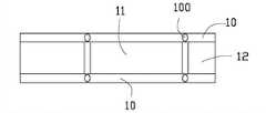
请参照图1及图2(其中图1为剖视图,图2为俯视图),步骤1,提供一基板10。具体地,该基板10开设若干贯穿基板10的孔洞100,且该基板10的上表面上设置第一电连接部11和第二电连接部12。所述第一电连接部11和第二电连接部12相互间隔。所述孔洞100设置于第一电连接部11和第二电连接部12之间的绝缘带的两端。Please refer to FIG. 1 and FIG. 2 (wherein FIG. 1 is a cross-sectional view and FIG. 2 is a top view), step 1, providing a
请同时参照图3及图4(其中图3为剖视图,图4为俯视图),步骤2,提供一发光二极管芯片30,设置该发光二极管芯片30于基板10上。具体地,该发光二极管芯片30设置在第一电连接部11的上表面上。所述发光二极管芯片30包括半导体发光结构31以及设置在半导体发光结构31顶部的第一电极34和第二电极35。所述第一电极34、第二电极35间隔设置在半导体发光结构31远离基板10的顶面上。所述第一电极34通过一导线32与第一电连接部11形成电性连接,所述第二电极35通过另一导线33与第二电连接部12形成电性连接。本实施例中,该基板10上设有两个发光二极管芯片30。具体实施时,所述发光二极管芯片30的个数不限于本实施例的情况,其可为三个,也可为多个。Please refer to FIG. 3 and FIG. 4 at the same time (where FIG. 3 is a cross-sectional view, and FIG. 4 is a top view), step 2, providing an
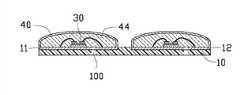
请同时参照图5及图6,步骤3,提供一透镜40,将该透镜40设置在该基板10上,该透镜40覆盖该发光二极管芯片30。具体地,该透镜40与该基板10之间形成一填充空间42,沿着该基板10的孔洞100填充封装材料到该填充空间42内,以在该透镜40与该基板10之间形成包覆该发光二极管芯片30的一封装层44。Please refer to FIG. 5 and FIG. 6 at the same time. In step 3, a
请同时参照图7,步骤4,提供一荧光粉薄膜50,将该荧光粉薄膜50设置在该透镜40上。具体地,该荧光粉薄膜50中均匀分布有荧光粉,荧光粉的材料可以为石榴石(garnet)结构的化合物。将该荧光粉薄膜50盖设在该透镜40上时,该荧光粉薄膜50为半凝固状态。由于该荧光粉薄膜50具有一定的伸缩强度和弹性,从而可以靠透镜40的支撑而不至于从各透镜40的孔隙处掉落。由于该荧光粉薄膜50为半凝固状态,因此其内部的荧光粉不会像流体状态的封装层一样发生沉积进而使荧光粉分布不均匀。Please refer to FIG. 7 at the same time, in step 4, a
步骤5,提供一具有毛细孔(图未示)的载板60,将该基板10设置在该载板60上。具体地,该载板60内具有连通载板60上下表面的毛细孔,该载板60的面积大于该基板10的面积。Step 5, providing a
请同时参照图8,步骤6,提供一模具70,该模具70与该载板60共同形成一收容空间711,荧光粉薄膜50及基板10收容在该收容空间711内。具体地,该模具70包括下模71及上模72,该下模71围设在该载板60周围,该上模22设置在该下模21上,该下模21的顶面及该荧光粉薄膜50的上表面处于同一平面,该上模22的底面与该下模21的顶面及该荧光粉薄膜50的上表面接触,该下模71、上模72及该载板60共同形成所述收容空间711。该上模72中央开设一贯穿孔720,一加压装置90设置在该贯穿孔720处。Please refer to FIG. 8 at the same time, in step 6, a
请同时参照图9,步骤7,通过载板60的毛细孔将收容空间711内的空气抽出与/或通过对该荧光粉薄膜50吹气的方式而使该荧光粉薄膜50贴附在透镜40上。具体地,提供一抽真空装置80,将该抽真空装置80对准该载板60的底部来抽离该收容空间711内的空气,使收容空间711内的空气沿着载板60的毛细孔流出。同时,加压装置90对该荧光粉薄膜50吹气以施加一个向下的、朝向透镜40的压力,使得该荧光粉薄膜50紧密地贴附在该透镜40表面。当然,具体实施过程中,上述抽真空装置80与加压装置90可只选择一种,即通过载板60的毛细孔将收容空间711内的空气抽出或通过对该荧光粉薄膜50吹气的方式而使该荧光粉薄膜50贴附在透镜40上。Please refer to FIG. 9 at the same time, step 7, the air in the
步骤8,通过高温烘烤使该荧光粉薄膜50固化至该透镜40。具体地,可先移除模具70、加压装置90、抽真空装置80及载板60,再通过高温烘烤使荧光粉薄膜50固化至该透镜40。当然,也可先固化荧光粉薄膜50,然后再移除模具70、加压装置90、抽真空装置80及载板60。最后,可将如图10所示的发光二极管封装结构沿着虚线切割,以获得多个发光二极管封装结构。Step 8, curing the
当然,上述制造方法中,该荧光粉薄膜50还可通过将收容空间711内的空气抽出与/或通过对该荧光粉薄膜50吹气的方式贴附在其他光学元件上,如封装层44上,即先直接在该发光二极管芯片30上覆盖封装层44,然后再通过将收容空间711内的空气抽出与/或通过对该荧光粉薄膜50吹气的方式将该荧光粉薄膜50贴附在封装层44上。Of course, in the above manufacturing method, the
本发明的发光二极管封装结构的制造方法中,先通过载板60的毛细孔将收容空间711内的空气抽出与/或通过对该荧光粉薄膜50吹气的方式而将该荧光粉薄膜50贴附在透镜40上,再将该荧光粉薄膜50固化在透镜40上,保证了荧光粉薄膜50中的荧光粉分布均匀、制作过程简便,避免了荧光粉喷涂或点胶工艺中出现的荧光粉分布不均的现象。In the manufacturing method of the light-emitting diode packaging structure of the present invention, the air in the receiving
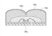
如图11所示为对应本发明另一实施例的发光二极管封装结构的制造方法制造的发光二极管封装结构的示意图。该另一实施例的制造方法与前述实施例的制造方法的区别在于:该另一实施例采用中心具有凹面46a的透镜40a,使该发光二极管芯片30a发出的光通过透镜40a后,形成蝙蝠翼形的光场而增加侧向出光。该透镜40a的外表面的中央为凹面,再通过采用空气抽出与/或通过对该荧光粉薄膜50a吹气的方式将荧光粉薄膜50a贴附在该透镜40a上,使荧光粉薄膜50a中的荧光粉在透镜40a表面均匀分布。而采用现有技术的制造方法将荧光粉薄膜贴附在中心具有凹面的透镜上,荧光粉更容易在透镜的凹面内沉积,导致荧光粉在透镜表面分布不均匀。所以本发明另一实施例的制造方法相对于现有技术的制造方法取得更优的技术效果。FIG. 11 is a schematic diagram of a light emitting diode packaging structure manufactured by a method for manufacturing a light emitting diode packaging structure corresponding to another embodiment of the present invention. The difference between the manufacturing method of this other embodiment and the manufacturing method of the previous embodiment is that this other embodiment adopts a
应该指出,上述实施方式仅为本发明的较佳实施方式,本领域技术人员还可在本发明精神内做其它变化。这些依据本发明精神所做的变化,都应包含在本发明所要求保护的范围之内。It should be pointed out that the above embodiments are only preferred embodiments of the present invention, and those skilled in the art can also make other changes within the spirit of the present invention. These changes made according to the spirit of the present invention should be included in the scope of protection of the present invention.
Claims (10)
Priority Applications (3)
| Application Number | Priority Date | Filing Date | Title |
|---|---|---|---|
| CN201210127471XACN103378263A (en) | 2012-04-27 | 2012-04-27 | Method for manufacturing light emitting diode encapsulating structure |
| TW101124468ATW201344989A (en) | 2012-04-27 | 2012-07-06 | Method for manufacturing light emitting diode package structure |
| US13/865,163US8828754B2 (en) | 2012-04-27 | 2013-04-17 | Method for manufacturing LED |
Applications Claiming Priority (1)
| Application Number | Priority Date | Filing Date | Title |
|---|---|---|---|
| CN201210127471XACN103378263A (en) | 2012-04-27 | 2012-04-27 | Method for manufacturing light emitting diode encapsulating structure |
Publications (1)
| Publication Number | Publication Date |
|---|---|
| CN103378263Atrue CN103378263A (en) | 2013-10-30 |
Family
ID=49463095
Family Applications (1)
| Application Number | Title | Priority Date | Filing Date |
|---|---|---|---|
| CN201210127471XAPendingCN103378263A (en) | 2012-04-27 | 2012-04-27 | Method for manufacturing light emitting diode encapsulating structure |
Country Status (3)
| Country | Link |
|---|---|
| US (1) | US8828754B2 (en) |
| CN (1) | CN103378263A (en) |
| TW (1) | TW201344989A (en) |
Cited By (1)
| Publication number | Priority date | Publication date | Assignee | Title |
|---|---|---|---|---|
| CN107256921A (en)* | 2017-05-27 | 2017-10-17 | 深圳雷曼光电科技股份有限公司 | COB LED encapsulation methods, display device and lighting device |
Families Citing this family (3)
| Publication number | Priority date | Publication date | Assignee | Title |
|---|---|---|---|---|
| DE102008054288A1 (en)* | 2008-11-03 | 2010-05-06 | Osram Gesellschaft mit beschränkter Haftung | Method for producing a flexible light strip |
| CN103311381A (en)* | 2012-03-13 | 2013-09-18 | 展晶科技(深圳)有限公司 | Production method for packaging structures of light-emitting diode |
| TWI634953B (en)* | 2017-03-28 | 2018-09-11 | 財團法人工業技術研究院 | Glue dispensing device and glue dispensing method |
Citations (5)
| Publication number | Priority date | Publication date | Assignee | Title |
|---|---|---|---|---|
| US6202276B1 (en)* | 1998-12-23 | 2001-03-20 | Tung-Han Chuang | Process for manufacturing an electromagnetic interference shielding superplastic alloy foil cladded outer shell product |
| CN101162750A (en)* | 2007-11-26 | 2008-04-16 | 佛山市国星光电股份有限公司 | Power LED with glue-filling formed bottom and manufacturing method thereof |
| US20110089455A1 (en)* | 2007-06-27 | 2011-04-21 | The Regents Of The University Of California | Optical designs for high-efficacy white-light emitting diodes |
| US20110127689A1 (en)* | 2009-12-01 | 2011-06-02 | Samsung Electro-Mechanics Co., Ltd. | Apparatus for manufacturing electronic component and method for manufacturing electronic component |
| US20110248305A1 (en)* | 2009-05-15 | 2011-10-13 | Archolux Inc. | Method for transferring a uniform phosphor layer on an article and light-emitting structure fabricated by the method |
Family Cites Families (6)
| Publication number | Priority date | Publication date | Assignee | Title |
|---|---|---|---|---|
| KR100761387B1 (en)* | 2005-07-13 | 2007-09-27 | 서울반도체 주식회사 | Mold for forming molding member and molding member forming method using same |
| CN100592538C (en)* | 2006-08-09 | 2010-02-24 | 广东昭信光电科技有限公司 | Packaging method of high-brightness white light-emitting diode |
| CN102356479A (en)* | 2009-03-19 | 2012-02-15 | 皇家飞利浦电子股份有限公司 | Illumination device with remote luminescent material |
| US9024341B2 (en)* | 2010-10-27 | 2015-05-05 | Taiwan Semiconductor Manufacturing Company, Ltd. | Refractive index tuning of wafer level package LEDs |
| US20120113621A1 (en)* | 2010-11-10 | 2012-05-10 | Taiwan Semiconductor Manufacturing Company, Ltd. | Batwing beam based led and backlight module using the same |
| US8759854B2 (en)* | 2011-05-24 | 2014-06-24 | Tsmc Solid State Lighting Ltd. | Bat-wing lens design with multi-die |
- 2012
- 2012-04-27CNCN201210127471XApatent/CN103378263A/enactivePending
- 2012-07-06TWTW101124468Apatent/TW201344989A/enunknown
- 2013
- 2013-04-17USUS13/865,163patent/US8828754B2/ennot_activeExpired - Fee Related
Patent Citations (5)
| Publication number | Priority date | Publication date | Assignee | Title |
|---|---|---|---|---|
| US6202276B1 (en)* | 1998-12-23 | 2001-03-20 | Tung-Han Chuang | Process for manufacturing an electromagnetic interference shielding superplastic alloy foil cladded outer shell product |
| US20110089455A1 (en)* | 2007-06-27 | 2011-04-21 | The Regents Of The University Of California | Optical designs for high-efficacy white-light emitting diodes |
| CN101162750A (en)* | 2007-11-26 | 2008-04-16 | 佛山市国星光电股份有限公司 | Power LED with glue-filling formed bottom and manufacturing method thereof |
| US20110248305A1 (en)* | 2009-05-15 | 2011-10-13 | Archolux Inc. | Method for transferring a uniform phosphor layer on an article and light-emitting structure fabricated by the method |
| US20110127689A1 (en)* | 2009-12-01 | 2011-06-02 | Samsung Electro-Mechanics Co., Ltd. | Apparatus for manufacturing electronic component and method for manufacturing electronic component |
Cited By (1)
| Publication number | Priority date | Publication date | Assignee | Title |
|---|---|---|---|---|
| CN107256921A (en)* | 2017-05-27 | 2017-10-17 | 深圳雷曼光电科技股份有限公司 | COB LED encapsulation methods, display device and lighting device |
Also Published As
| Publication number | Publication date |
|---|---|
| US20130288408A1 (en) | 2013-10-31 |
| TW201344989A (en) | 2013-11-01 |
| US8828754B2 (en) | 2014-09-09 |
Similar Documents
| Publication | Publication Date | Title |
|---|---|---|
| US8809083B2 (en) | Method of manufacturing light emitting diode | |
| TWI630731B (en) | White light emitting diode component | |
| CN103022325B (en) | The LED encapsulation structure of application long distance formula phosphor powder layer and method for making thereof | |
| US9012248B2 (en) | Method for packaging light emitting diode | |
| CN105023992A (en) | Packaging method and packaging structure | |
| CN101551068A (en) | Light emitting diode device and encapsulating method thereof | |
| US20120021542A1 (en) | Method of packaging light emitting device | |
| US8883533B2 (en) | Method for manufacturing light emitting diode package | |
| CN105280781B (en) | A kind of upside-down mounting white light LED part and preparation method thereof | |
| CN102479785A (en) | Light-emitting structure with deposited fluorescent coating layer and manufacturing method thereof | |
| CN103254889B (en) | Fluorescent powder film making method and corresponding LED encapsulation method | |
| CN103378263A (en) | Method for manufacturing light emitting diode encapsulating structure | |
| CN102760822B (en) | Light-emitting diode encapsulation structure and manufacturing method thereof | |
| CN106449621A (en) | LED (light emitting diode) encapsulation method and structure thereof | |
| CN104993032A (en) | White-light LED device and manufacturing method thereof | |
| US20130285096A1 (en) | Light emitting diode package and method for manufacturing the same | |
| CN103515518A (en) | Encapsulating method of light emitting diode | |
| CN103378260A (en) | Method for manufacturing packaging structure of light emitting diode | |
| CN107346801A (en) | LED integrated encapsulation structures and its method for packing | |
| CN104282820A (en) | Light-emitting diode and encapsulating method thereof | |
| CN102916089B (en) | Method for forming packaging structure of light emitting diode and method for forming base of packaging structure | |
| CN103855281A (en) | LED and manufacturing method thereof | |
| CN102487110A (en) | LED packaging method | |
| US8765499B2 (en) | Method for manufacturing LED package | |
| CN103426977B (en) | LED encapsulation method |
Legal Events
| Date | Code | Title | Description |
|---|---|---|---|
| C06 | Publication | ||
| PB01 | Publication | ||
| C10 | Entry into substantive examination | ||
| SE01 | Entry into force of request for substantive examination | ||
| C02 | Deemed withdrawal of patent application after publication (patent law 2001) | ||
| WD01 | Invention patent application deemed withdrawn after publication | Application publication date:20131030 |