CN103377161A - Main board and data processing method applied to same - Google Patents
Main board and data processing method applied to sameDownload PDFInfo
- Publication number
- CN103377161A CN103377161ACN2012101215444ACN201210121544ACN103377161ACN 103377161 ACN103377161 ACN 103377161ACN 2012101215444 ACN2012101215444 ACN 2012101215444ACN 201210121544 ACN201210121544 ACN 201210121544ACN 103377161 ACN103377161 ACN 103377161A
- Authority
- CN
- China
- Prior art keywords
- cpu
- dma controller
- data
- unit
- bus
- Prior art date
- Legal status (The legal status is an assumption and is not a legal conclusion. Google has not performed a legal analysis and makes no representation as to the accuracy of the status listed.)
- Pending
Links
Images


Classifications
- G—PHYSICS
- G06—COMPUTING OR CALCULATING; COUNTING
- G06F—ELECTRIC DIGITAL DATA PROCESSING
- G06F13/00—Interconnection of, or transfer of information or other signals between, memories, input/output devices or central processing units
- G06F13/14—Handling requests for interconnection or transfer
- G06F13/16—Handling requests for interconnection or transfer for access to memory bus
- G06F13/1668—Details of memory controller
Landscapes
- Engineering & Computer Science (AREA)
- Theoretical Computer Science (AREA)
- Physics & Mathematics (AREA)
- General Engineering & Computer Science (AREA)
- General Physics & Mathematics (AREA)
- Bus Control (AREA)
- Multi Processors (AREA)
Abstract
Translated fromChineseDescription
Translated fromChinese技术领域technical field
本发明涉及一种主板及应用于该主板的数据处理方法,特别涉及一种使用DMAC(Direct Memory Access Controller,直接内存访问控制器)进行数据传输控制的主板及应用于该主板的处理方法。The present invention relates to a main board and a data processing method applied to the main board, in particular to a main board using DMAC (Direct Memory Access Controller) for data transmission control and a processing method applied to the main board.
背景技术Background technique
现有的主板都会设有多条DIMM(Dual Inline Memory Modules,双列直插式存储模块)类型的内存插槽以供内存条插接,外部存储设备(如硬盘)则通过专有的SATA接口与主板相连。当外部存储设备与内存进行成批的数据交换时,CPU(Central Processing Unit,中央处理器)会将总线的控制权交给DMA控制器,以通过DMA控制器来控制外部存储设备与内存条之间的数据传输,从而有利于减轻CPU的负担。然而,主板上的DIMM插槽通常不会全部插接有内存条,如此使得多余的DIMM插槽经常处于空闲状态,从而降低了计算机硬件资源的利用率。Existing motherboards will be equipped with multiple DIMM (Dual Inline Memory Modules, Dual Inline Memory Modules) type memory slots for memory sticks to be plugged in, and external storage devices (such as hard disks) are connected through a proprietary SATA interface. Connect to the motherboard. When the external storage device and the memory exchange data in batches, the CPU (Central Processing Unit, central processing unit) will hand over the control of the bus to the DMA controller to control the connection between the external storage device and the memory stick through the DMA controller. Between the data transmission, which is conducive to reducing the burden on the CPU. However, usually not all the DIMM slots on the motherboard are plugged with memory modules, so that the redundant DIMM slots are often in an idle state, thereby reducing the utilization rate of computer hardware resources.
发明内容Contents of the invention
鉴于以上内容,有必要提供一种可实现与DIMM插槽相连的外部存储介质与内存之间的数据传输的主板及应用于该主板的数据处理方法,进而得以提高计算机硬件资源利用率。In view of the above, it is necessary to provide a motherboard that can realize data transmission between an external storage medium connected to a DIMM slot and a memory and a data processing method applied to the motherboard, thereby improving the utilization rate of computer hardware resources.
一种主板,包括:A motherboard, comprising:
一CPU;a CPU;
一第一DMA控制器;a first DMA controller;
一内存模块,通过一第一DIMM插槽与一第一总线相连;以及A memory module connected to a first bus through a first DIMM slot; and
一外部存储装置,通过一第二DIMM插槽与该第一总线相连,该外部存储装置包括:An external storage device is connected to the first bus through a second DIMM slot, and the external storage device includes:
一存储体;a storage body;
一第二总线;a second bus;
一第一缓存单元,与该第二总线相连;a first cache unit connected to the second bus;
一接口控制单元,与该第二总线及第二DIMM插槽相连,该接口控制单元用于接收该CPU通过该第二DIMM插槽输出的对存储体进行读操作的读取控制指令及进行写操作的写入控制指令并执行相应的操作;以及An interface control unit, connected with the second bus and the second DIMM slot, the interface control unit is used to receive the read control instruction and write the memory bank output by the CPU through the second DIMM slot write control instructions for the operation and execute the corresponding operation; and
一第二DMA控制器,用于控制该第一缓存单元与该存储体之间的数据传输;A second DMA controller, used to control the data transmission between the first cache unit and the storage bank;
当该CPU输出对该存储体进行读操作的读取控制指令时,该接口控制单元接收该读操作的控制指令,该CPU还对该第二DMA控制器的相关寄存器进行设定,以通过该第二DMA控制器将该存储体的数据读出至该第一缓存单元;当数据传输完毕时,该第二DMA控制器产生一中断至该CPU,该CPU对该第一DMA控制器的相关寄存器进行设定,以通过该第一DMA控制器将该第一缓存单元的数据传输至该内存模块;When the CPU outputs a read control instruction for reading the memory bank, the interface control unit receives the control instruction for the read operation, and the CPU also sets the relevant registers of the second DMA controller to pass the The second DMA controller reads out the data of the storage bank to the first cache unit; when the data transmission is completed, the second DMA controller generates an interrupt to the CPU, and the CPU's correlation with the first DMA controller The register is set to transmit the data of the first cache unit to the memory module through the first DMA controller;
当该CPU输出对该存储体进行写操作的控制指令时,该CPU对该第一DMA控制器的相关寄存器进行设定,以将该内存模块的数据读出至该第一缓存单元;当数据传输完毕时,该第一DMA控制器产生一中断至该CPU,该CPU输出写入控制指令至该接口控制单元,还对该第二DMA控制器的相关寄存器进行设定,该第二DMA控制器将该第一缓存单元的数据写入至该存储体。When the CPU outputs a control command for writing the memory bank, the CPU sets the relevant registers of the first DMA controller to read the data of the memory module to the first cache unit; when the data When the transmission is completed, the first DMA controller generates an interrupt to the CPU, and the CPU outputs the write control command to the interface control unit, and also sets the relevant registers of the second DMA controller, and the second DMA controls The device writes the data of the first cache unit to the storage bank.
一种数据处理方法,应用于一插接于一主板的第一DIMM插槽的外部存储装置与一插接于一第二DIMM插槽的内存模块进行数据交换,其中该第一DIMM插槽及第二DIMM插槽通过一第一总线相连,一CPU通过一第一DMA控制器对该外部存储装置进行读操作或写操作,该外部存储装置包括一存储体、一第二总线、一与该第二总线相连的第一缓存单元、一与该第二总线及第二DIMM插槽相连的接口控制单元以及一第二DMA控制器;该数据处理方法包括如下步骤:A data processing method, applied to an external storage device plugged into a first DIMM slot of a motherboard to exchange data with a memory module plugged into a second DIMM slot, wherein the first DIMM slot and The second DIMM slot is connected through a first bus, and a CPU reads or writes the external storage device through a first DMA controller, and the external storage device includes a memory bank, a second bus, and the external storage device. The first cache unit connected to the second bus, an interface control unit connected to the second bus and the second DIMM slot, and a second DMA controller; the data processing method includes the following steps:
判断对该存储体进行读操作还是写操作;Determine whether to perform a read operation or a write operation on the memory bank;
当对该存储体进行读操作时:When reading from this memory bank:
传输读取控制指令至该接口控制单元,并对该第二DMA控制器的寄存器进行设定;transmit the read control instruction to the interface control unit, and set the register of the second DMA controller;
该第二DMA控制器通过该接口控制单元将该存储体的数据读出至该第一缓存单元;The second DMA controller reads the data of the storage bank to the first cache unit through the interface control unit;
当数据传输完毕时,产生一中断信号至该CPU;When the data transmission is completed, an interrupt signal is generated to the CPU;
对该第一DMA控制器的相关寄存器进行设定;Setting relevant registers of the first DMA controller;
该第一DMA控制器将该第一缓存单元中的数据传输至该内存模块;The first DMA controller transfers the data in the first cache unit to the memory module;
当数据传输完毕时,产生一中断信号至该CPU;When the data transmission is completed, an interrupt signal is generated to the CPU;
当对该存储体写操作时:When writing to this memory bank:
传输写入控制指令至该接口控制单元,并对该第一DMA控制器寄存器进行设定;transmitting a write control command to the interface control unit, and setting the first DMA controller register;
该第一DMA控制器将该内存模块中的数据读出至该第一缓存单元;The first DMA controller reads the data in the memory module to the first cache unit;
当数据传输完毕时,该第一DMA控制器产生一中断信号至该CPU;When the data transmission is completed, the first DMA controller generates an interrupt signal to the CPU;
该CPU对该第二DMA控制器的相关寄存器进行设定;The CPU sets the relevant registers of the second DMA controller;
该第二DMA将该第一缓存单元的数据写入该存储体;The second DMA writes the data of the first cache unit into the memory bank;
当数据写入完成时,该第二DMA控制器产生一中断信号至该CPU。When data writing is completed, the second DMA controller generates an interrupt signal to the CPU.
上述主板及应用于该主板的数据处理方法通过将外部存储装置插接于该主板上无内存条插接的DIMM插槽,如此使得连接于DIMM插槽的外部存储装置与内存模块之间的数据以DMA模式进行传输,进而提高了计算机的资源利用率。The above-mentioned mainboard and the data processing method applied to the mainboard make the data between the external storage device and the memory module connected to the DIMM slots be The transmission is carried out in DMA mode, thereby improving the resource utilization rate of the computer.
附图说明Description of drawings
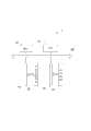
图1是本发明主板的较佳实施方式的示意图。FIG. 1 is a schematic diagram of a preferred embodiment of the motherboard of the present invention.
图2是图1中外部存储装置的的较佳实施方式的方框图。FIG. 2 is a block diagram of a preferred embodiment of the external storage device in FIG. 1 .
图3是本发明数据处理方法的较佳实施方式的流程图。Fig. 3 is a flowchart of a preferred embodiment of the data processing method of the present invention.
主要元件符号说明Description of main component symbols
如下具体实施方式将结合上述附图进一步说明本发明。The following specific embodiments will further illustrate the present invention in conjunction with the above-mentioned drawings.
具体实施方式Detailed ways
请参考图1,本发明主板1的较佳实施方式包括一插接于一第一DIMM插槽40的外部存储装置30、一插接于一第二DIMM插槽60的内存模块70及一DMAC (DMA Controller,DMA控制器)20以及通过该DMAC 20对该外部存储装置30以DMA模式进行读操作或写操作的CPU 10,其中该第一DIMM插槽40及第二DIMM插槽60通过一第一总线80相互连接。Please refer to Fig. 1, the preferred embodiment of motherboard 1 of the present invention comprises an
请参考图2,该外部存储装置30的较佳实施方式包括一第二总线90、一与该第二总线90及该第一DIMM插槽40均相连的开关单元300及LDMAC(Local DMA Controller,本地DMA控制器)301、一与该第二总线90相连的第一缓存单元302及第二缓存单元305、一通过该第二缓存单元305连接于该第二总线90的接口控制单元303及一与该接口控制单元303相连的存储体50,其中该LDMAC 301亦为一DMA控制器,该主板1使用了该第一DIMM插槽40的未定义的空闲引脚以对该外部存储装置30进行控制。本实施方式中,该存储体50为一固态硬盘。Please refer to Fig. 2, the preferred implementation manner of this
该开关单元300用于接收该CPU 10输出的开关信号来控制该外部存储装置30与该第一总线80之间数据传输的连通与断开。如当该开关单元300接收到一第一开关信号时,该开关单元300则控制该外部存储装置30与该第一总线80之间处于连通状态,即该外部存储装置30与该第一总线80之间可进行数据传输;当该开关单元300接收到一第二开关信号时,该开关单元300则控制该外部存储装置30与该第一总线80之间处于断开状态,即该外部存储装置30与该第一总线80之间禁止数据传输。根据计算机组成原理可知,计算机系统包括数据总线、地址总线及控制总线,其中数据总线用于传输数据,控制总线用于传输控制信号,地址总线用于寻址。本实施方式中,该开关单元300只用于控制该外部存储装置30与该第一DIMM插槽40之间的数据传输。当然,在其他实施方式中,该开关单元300亦可省略,此时,该第二总线90则直接与该第一DIMM插槽40相连接。The
该接口控制单元303用于接收该CPU 10输出的控制指令,以对该存储体50进行相应的操作,如从该存储体50中读取数据或向该存储体50中写入数据。The
该LDMAC 301用于控制该第二缓存单元305与该第一缓存单元302之间的数据传输。The LDMAC 301 is used to control data transmission between the
该第一缓存单元302用于缓存对该存储体50写入的数据,即当需要将内存模块70内的数据写入到存储体50内时,该内存模块70中的数据由该DMAC 20预先存储至该第一缓存单元302,之后,由该LDMAC 301再将该第一缓存单元302中的数据写入该存储体50。The
该第二缓存单元305用于缓存从该存储体50中读取的数据,如当该接口控制单元303接收该CPU 10输出的读取控制指令时,该接口控制单元303可预先从该存储体50中读取数据,并将其存储至该第二缓存单元305,之后,由该LDMAC 301将该第二缓存单元305中的数据传输至该第一缓存单元302。The
当该CPU 10对该存储体50进行读操作时,该CPU 10输出第一开关信号至该开关单元300,以使得该开关单元300处于连通状态;同时,该CPU 10还对该LDMAC 301的相关寄存器进行相应的设定,以对该LDMAC 301进行初始化。同时,该CPU 10还输出对应的读取控制指令至该接口控制单元303,以将该存储体50的数据预先读取至该第二缓存单元305。之后,该CPU 10输出第二开关信号至该开关单元300,以断开该外部存储装置30与该第一总线80的连接。该LDMAC 301将存储于该第二缓存单元305内的数据读出至该第一缓存单元302。当数据传输完毕时,该LDMAC 301产生一中断信号至该CPU 10,以通知该CPU 10。该CPU 10接收到该LDMAC 301输出的中断信号后,输出第一开关信号至该开关单元300,以使得该外部存储装置30与该第一总线80再次处于连通状态;同时,该CPU 10还对该DMAC 20的相关寄存器进行设定,以对该DMAC 20进行初始化工作。之后,该DMAC 20将该第一缓存单元302内的数据通过该第二总线90及该第一总线80传输至该内存模块70。当数据传输完成后,该DMAC 20产生一中断信号至CPU 10,并将该第一总线80的控制权交给该CPU 10,如此即完成了对该存储体50的读操作。When the
在其他实施方式中,该第二缓存单元305亦可省略,如此当对该存储体50进行读操作时,该LDMAC 301则直接通过该接口控制单元303读取该存储体50的数据,并将该数据传输至该第一缓存单元302内即可。In other embodiments, the
当该CPU 10对该存储体50进行写操作时,该CPU 10输出第一开关信号至该开关单元300,以使得该开关单元300处于连通状态;该CPU 10还对该DMAC 304的相关寄存器进行相应的设定,以对该DMAC 20进行初始化。之后,该DMAC 20将该内存模块70内的数据通过该第一总线80及该第二总线90传输至该第一缓存单元302。当数据传输完毕时,该DMAC 20输出一中断信号至该CPU 10,以将该第一总线80的控制权交给该CPU 10。之后,该CPU 10对该LDMAC 301的相关寄存器进行设定,还输出相应的写入控制指令至该接口控制单元303。之后,该CPU 10输出第二开关信号至该开关单元300,以使得该外部存储装置30与该第一总线80处于断开状态。之后,该LDMAC 301将该第一缓存单元302的数据存储于该第二缓存单元305,该接口控制单元303读取该第二缓存单元305数据并将该数据写入该存储体50内。当数据传输完毕时,该LDMAC 301产生一中断信号至该CPU 10,以通知该CPU 10完成对该存储体50的写操作。如此即完成了对该存储体50的写操作。When the
在其他实施方式中,当该第二缓存单元305省略时,该LDMAC 301则直接将该第一缓存单元302内的数据通过该接口控制单元303写入该存储体50内。In other embodiments, when the
请参考图3,本发明数据处理方法的较佳实施方式包括如下步骤:Please refer to Fig. 3, the preferred embodiment of the data processing method of the present invention comprises the following steps:
步骤S10,控制该开关单元300处于连通状态。该CPU 10通过输出第一开关信号至该开关单元300以使得该外部存储装置30与该第一总线80处于连通状态。Step S10, controlling the
步骤S11,判断对该存储体50进行的是读操作还是写操作,当该CPU 10对该存储体50进行读操作时,进入步骤S12;否则,当该CPU 10对该存储体50进行写操作时,进入步骤S22。Step S11, judging whether the
步骤S12,传输相应的读取控制指令至该接口控制单元303,以读取该存储体50的数据至该第二缓存单元305,并对该LDMAC 301的相关寄存器进行设定。Step S12, transmit the corresponding read control command to the
步骤S13,控制该开关单元300处于断开状态。该CPU 10输出第二开关信号至该开关单元300以断开该第二总线90与该第一总线80之间的连接。Step S13, controlling the
步骤S14,该LDMAC 301将该第二缓存单元305的数据读出至该第一缓存单元302。Step S14, the
步骤S15,判断数据是否传输完毕,当数据传输完毕时,进入步骤S16;否则,当数据未传输完毕时,返回步骤S14。Step S15, judging whether the data transmission is complete, and when the data transmission is complete, proceed to step S16; otherwise, when the data transmission is not complete, return to step S14.
步骤S16,产生一中断信号至该CPU 10。数据传输完毕时,该LDMAC 301通过发送一中断信号给该CPU 10,以通知该CPU 10。Step S16, generating an interrupt signal to the
步骤S17,控制该开关单元300处于连通状态,并对该DMAC 20的相关寄存器进行设定。Step S17, control the
步骤S18,该DMAC 20将该第一缓存单元302内的数据通过该第二总线90及该第一总线80传输至该内存模块70。Step S18, the
步骤S19,该DMAC 20产生一中断信号至CPU 10,以将对该第一总线80的控制权交给该CPU 10。当该第一缓存单元302内的数据传输完毕时,该DMAC 20则将该第一总线80的控制权交给该CPU 10,以便该CPU 10进行其他的程序处理。Step S19, the
步骤S22,对该DMAC 20的相关寄存器进行设定。该CPU 10对该DMAC 20的相关寄存器进行设定,以完成对该DMAC 20的初始化工作。Step S22, setting the relevant registers of the
步骤S23,该DMAC 20将该内存模块70内的数据通过该第一总线80及该第二总线90存储于该第一缓存单元302。Step S23, the
步骤S24,判断数据是否传输完毕,当数据传输完毕时,进入步骤S25;否则,当数据未传输完毕时,返回步骤S23。Step S24, judging whether the data transmission is complete, when the data transmission is complete, enter step S25; otherwise, when the data transmission is not complete, return to step S23.
步骤S25,传输相应的写入控制指令至该接口控制单元303,并对该LDMAC 301的相关寄存器进行设定。Step S25, transmit the corresponding write control command to the
步骤S26,控制该开关单元300处于断开状态。该CPU 10输出第二开关信号至该开关单元300以断开该外部存储装置30与该第一总线80之间的连接。Step S26, controlling the
步骤S27,该LDMAC 301通过该接口控制单元303将该第一缓存单元302的数据写入该存储体50。Step S27, the
步骤S28,该LDMAC 301产生一中断信号至CPU 10,以通知该CPU 10,已完成对该存储体50的写操作。Step S28, the
上述主板及应用于该主板的数据处理方法通过将外部存储装置30插接于该主板1上无内存条插接的DIMM插槽,如此使得连接于DIMM插槽的外部存储装置30与内存模块70之间的数据以DMA模式进行传输,进而提高了计算机的资源利用率。The above-mentioned main board and the data processing method applied to the main board make the
Claims (9)
Translated fromChinesePriority Applications (3)
| Application Number | Priority Date | Filing Date | Title |
|---|---|---|---|
| CN2012101215444ACN103377161A (en) | 2012-04-24 | 2012-04-24 | Main board and data processing method applied to same |
| TW101115530ATW201344444A (en) | 2012-04-24 | 2012-05-02 | Motherboard and data processing method thereof |
| US13/772,396US20130282971A1 (en) | 2012-04-24 | 2013-02-21 | Computing system and data transmission method |
Applications Claiming Priority (1)
| Application Number | Priority Date | Filing Date | Title |
|---|---|---|---|
| CN2012101215444ACN103377161A (en) | 2012-04-24 | 2012-04-24 | Main board and data processing method applied to same |
Publications (1)
| Publication Number | Publication Date |
|---|---|
| CN103377161Atrue CN103377161A (en) | 2013-10-30 |
Family
ID=49381236
Family Applications (1)
| Application Number | Title | Priority Date | Filing Date |
|---|---|---|---|
| CN2012101215444APendingCN103377161A (en) | 2012-04-24 | 2012-04-24 | Main board and data processing method applied to same |
Country Status (3)
| Country | Link |
|---|---|
| US (1) | US20130282971A1 (en) |
| CN (1) | CN103377161A (en) |
| TW (1) | TW201344444A (en) |
Cited By (1)
| Publication number | Priority date | Publication date | Assignee | Title |
|---|---|---|---|---|
| CN108197504A (en)* | 2017-12-28 | 2018-06-22 | 湖南国科微电子股份有限公司 | A kind of controlled data encrypting and deciphering system and method |
Families Citing this family (5)
| Publication number | Priority date | Publication date | Assignee | Title |
|---|---|---|---|---|
| CN205540398U (en)* | 2015-05-29 | 2016-08-31 | 无锡中太服务器有限公司 | Sub - card of memory, mainboard and quick -witted case |
| CN105117180B (en)* | 2015-09-28 | 2018-08-17 | 北京联想核芯科技有限公司 | A kind of date storage method and device and solid state disk |
| CN108874703A (en)* | 2017-05-10 | 2018-11-23 | 瑞昱半导体股份有限公司 | Expanding unit and storage system |
| US12411693B2 (en) | 2020-12-30 | 2025-09-09 | Silicon Laboratories Inc. | Apparatus for processor with hardware fence and associated methods |
| CN116932451A (en)* | 2022-03-31 | 2023-10-24 | 华为技术有限公司 | A data processing method, host and related equipment |
Family Cites Families (13)
| Publication number | Priority date | Publication date | Assignee | Title |
|---|---|---|---|---|
| US7424552B2 (en)* | 1997-12-17 | 2008-09-09 | Src Computers, Inc. | Switch/network adapter port incorporating shared memory resources selectively accessible by a direct execution logic element and one or more dense logic devices |
| US20040236877A1 (en)* | 1997-12-17 | 2004-11-25 | Lee A. Burton | Switch/network adapter port incorporating shared memory resources selectively accessible by a direct execution logic element and one or more dense logic devices in a fully buffered dual in-line memory module format (FB-DIMM) |
| US7062591B2 (en)* | 2001-09-28 | 2006-06-13 | Dot Hill Systems Corp. | Controller data sharing using a modular DMA architecture |
| US6854042B1 (en)* | 2002-07-22 | 2005-02-08 | Chris Karabatsos | High-speed data-rate converting and switching circuit |
| US8019938B2 (en)* | 2006-12-06 | 2011-09-13 | Fusion-I0, Inc. | Apparatus, system, and method for solid-state storage as cache for high-capacity, non-volatile storage |
| US7975109B2 (en)* | 2007-05-30 | 2011-07-05 | Schooner Information Technology, Inc. | System including a fine-grained memory and a less-fine-grained memory |
| US9672169B2 (en)* | 2010-06-30 | 2017-06-06 | Texas Instruments Incorporated | Dual in line memory module with multiple memory interfaces |
| US8713379B2 (en)* | 2011-02-08 | 2014-04-29 | Diablo Technologies Inc. | System and method of interfacing co-processors and input/output devices via a main memory system |
| US8694721B2 (en)* | 2011-04-11 | 2014-04-08 | Inphi Corporation | Memory buffer with one or more auxiliary interfaces |
| US20130067156A1 (en)* | 2011-09-12 | 2013-03-14 | Byungcheol Cho | Double data rate controller having shared address and separate data error correction |
| US8874680B1 (en)* | 2011-11-03 | 2014-10-28 | Netapp, Inc. | Interconnect delivery process |
| JP5962260B2 (en)* | 2012-06-29 | 2016-08-03 | 富士通株式会社 | Storage device and write completion notification method |
| US9250954B2 (en)* | 2013-01-17 | 2016-02-02 | Xockets, Inc. | Offload processor modules for connection to system memory, and corresponding methods and systems |
- 2012
- 2012-04-24CNCN2012101215444Apatent/CN103377161A/enactivePending
- 2012-05-02TWTW101115530Apatent/TW201344444A/enunknown
- 2013
- 2013-02-21USUS13/772,396patent/US20130282971A1/ennot_activeAbandoned
Cited By (2)
| Publication number | Priority date | Publication date | Assignee | Title |
|---|---|---|---|---|
| CN108197504A (en)* | 2017-12-28 | 2018-06-22 | 湖南国科微电子股份有限公司 | A kind of controlled data encrypting and deciphering system and method |
| CN108197504B (en)* | 2017-12-28 | 2022-01-11 | 湖南国科微电子股份有限公司 | Controllable data encryption and decryption system and method |
Also Published As
| Publication number | Publication date |
|---|---|
| US20130282971A1 (en) | 2013-10-24 |
| TW201344444A (en) | 2013-11-01 |
Similar Documents
| Publication | Publication Date | Title |
|---|---|---|
| CN108268414B (en) | SD card driver and its control method based on SPI mode | |
| US10795424B2 (en) | Server power saving system and server power saving method | |
| CN103377161A (en) | Main board and data processing method applied to same | |
| TWI665554B (en) | Hot swap control circuit and related storage server system | |
| US20120210038A1 (en) | External bridge system | |
| EP1963977B1 (en) | Memory systems with memory chips down and up | |
| US8883521B2 (en) | Control method of multi-chip package memory device | |
| CN114816254A (en) | Hard disk data access method, device, equipment and medium | |
| US20100023669A1 (en) | Host controller disposed in multi-function card reader | |
| CN106407145A (en) | An interface access method and system and a memory card | |
| US20220342835A1 (en) | Method and apparatus for disaggregation of computing resources | |
| US9298378B2 (en) | Logic device | |
| US11983443B2 (en) | Multi-access memory modules | |
| US10853255B2 (en) | Apparatus and method of optimizing memory transactions to persistent memory using an architectural data mover | |
| TW201112130A (en) | Controllers and methods for controlling data transfer, and electronic systems | |
| TW201824279A (en) | Non-volatile memory device and method of operating data storage device therewith | |
| US20200379677A1 (en) | Memory controller and memory controlling method where number of commands (executed by the memory controller prior to releasing host memory) is adjusted based on transmission speed of interface to host | |
| CN102866755A (en) | Power-on reset device for integrated test system | |
| CN117349212A (en) | Server main board and solid state disk insertion detection method thereof | |
| TWI714116B (en) | Memory controller, memory controlling method, and computer system | |
| TWI683254B (en) | Server power saving system and power saving method thereof | |
| CN106325377B (en) | The data processing method of Principle of External Device Extension card and I/O peripheral equipment | |
| CN208077160U (en) | SD card driver based on SPI mode | |
| RU2402064C2 (en) | Server | |
| CN221960541U (en) | Display card device and microprocessor device |
Legal Events
| Date | Code | Title | Description |
|---|---|---|---|
| C06 | Publication | ||
| PB01 | Publication | ||
| C02 | Deemed withdrawal of patent application after publication (patent law 2001) | ||
| WD01 | Invention patent application deemed withdrawn after publication | Application publication date:20131030 |