CN103376748A - Electronic device - Google Patents
Electronic deviceDownload PDFInfo
- Publication number
- CN103376748A CN103376748ACN2012101174514ACN201210117451ACN103376748ACN 103376748 ACN103376748 ACN 103376748ACN 2012101174514 ACN2012101174514 ACN 2012101174514ACN 201210117451 ACN201210117451 ACN 201210117451ACN 103376748 ACN103376748 ACN 103376748A
- Authority
- CN
- China
- Prior art keywords
- unit
- control
- electronic device
- pin
- signal
- Prior art date
- Legal status (The legal status is an assumption and is not a legal conclusion. Google has not performed a legal analysis and makes no representation as to the accuracy of the status listed.)
- Pending
Links
Images
Classifications
- G—PHYSICS
- G05—CONTROLLING; REGULATING
- G05B—CONTROL OR REGULATING SYSTEMS IN GENERAL; FUNCTIONAL ELEMENTS OF SUCH SYSTEMS; MONITORING OR TESTING ARRANGEMENTS FOR SUCH SYSTEMS OR ELEMENTS
- G05B19/00—Programme-control systems
- G05B19/02—Programme-control systems electric
- G05B19/04—Programme control other than numerical control, i.e. in sequence controllers or logic controllers
- G05B19/042—Programme control other than numerical control, i.e. in sequence controllers or logic controllers using digital processors
- G—PHYSICS
- G05—CONTROLLING; REGULATING
- G05B—CONTROL OR REGULATING SYSTEMS IN GENERAL; FUNCTIONAL ELEMENTS OF SUCH SYSTEMS; MONITORING OR TESTING ARRANGEMENTS FOR SUCH SYSTEMS OR ELEMENTS
- G05B2219/00—Program-control systems
- G05B2219/20—Pc systems
- G05B2219/23—Pc programming
- G05B2219/23316—Standby, inactive, sleep or active, operation mode
- G—PHYSICS
- G05—CONTROLLING; REGULATING
- G05B—CONTROL OR REGULATING SYSTEMS IN GENERAL; FUNCTIONAL ELEMENTS OF SUCH SYSTEMS; MONITORING OR TESTING ARRANGEMENTS FOR SUCH SYSTEMS OR ELEMENTS
- G05B2219/00—Program-control systems
- G05B2219/20—Pc systems
- G05B2219/25—Pc structure of the system
- G05B2219/25291—Set module, component to sleep if no event or no other module needs it
Landscapes
- Physics & Mathematics (AREA)
- General Physics & Mathematics (AREA)
- Engineering & Computer Science (AREA)
- Automation & Control Theory (AREA)
- Direct Current Feeding And Distribution (AREA)
- Power Sources (AREA)
Abstract
Translated fromChinese
Description
Translated fromChinese技术领域technical field
本发明涉及一种电子设备。The invention relates to an electronic device.
背景技术Background technique
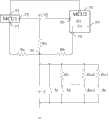
现有技术中,具有唤醒功能的电子设备,可在待机状态下通过按压任意按键将电子设备切换至工作状态。如图1所示,第一控制芯片MCU1具有第一上电引脚P1、第一侦测引脚P2、第一控制引脚P3。第二控制芯片MCU2具有第二上电引脚P4、第二控制引脚P5、第二侦测引脚P6及接地引脚P7。第一上电引脚P1与第一电压源V1电性连接,第一侦测引脚P2通过第一结点N1及第一电阻Ra与第一电压源V1电性连接,第二控制引脚P3与第二控制引脚P5电性连接。第二上电引脚P4与第二电压源V2电性连接,第二侦测引脚P6与第一结点N1电性连接,接地引脚P7接地。每个按键与一个分压电阻串联连接后与其他按键并联连接于第一结点N1和地之间。在电子设备处于待机状态时,第二控制芯片MCU2断开与第二电压源V2之间的电性连接。第一控制芯片MCU1接收第一电压源V1的供电电压上电工作,并通过第一侦测引脚P2侦测第一结点N1的电压。当按压任意一个按键,使得第一结点N1的电压不等于预定值,第一控制芯片MCU1输出第一控制信号给第二控制引脚P5。第二控制引脚P5根据第一控制信号建立第二控制芯片MCU2与第二电压源V2之间的电性连接,电子设备切换至工作状态。此时,通过第二侦测引脚P6侦测第一结点N1的电压值控制第二控制芯片MCU2执行被按压按键对应的功能。In the prior art, an electronic device with a wake-up function can switch the electronic device to a working state by pressing any key in a standby state. As shown in FIG. 1 , the first control chip MCU1 has a first power-on pin P1 , a first detection pin P2 , and a first control pin P3 . The second control chip MCU2 has a second power-on pin P4, a second control pin P5, a second detection pin P6 and a ground pin P7. The first power-on pin P1 is electrically connected to the first voltage source V1, the first detection pin P2 is electrically connected to the first voltage source V1 through the first node N1 and the first resistor Ra, and the second control pin P3 is electrically connected to the second control pin P5. The second power-on pin P4 is electrically connected to the second voltage source V2, the second detection pin P6 is electrically connected to the first node N1, and the ground pin P7 is grounded. Each button is connected in series with a voltage dividing resistor and then connected in parallel with other buttons between the first node N1 and the ground. When the electronic device is in the standby state, the second control chip MCU2 is electrically disconnected from the second voltage source V2. The first control chip MCU1 receives the power supply voltage of the first voltage source V1 for power-on operation, and detects the voltage of the first node N1 through the first detection pin P2. When any button is pressed so that the voltage of the first node N1 is not equal to the predetermined value, the first control chip MCU1 outputs a first control signal to the second control pin P5. The second control pin P5 establishes an electrical connection between the second control chip MCU2 and the second voltage source V2 according to the first control signal, and the electronic device switches to the working state. At this time, the voltage value of the first node N1 is detected by the second detection pin P6 to control the second control chip MCU2 to execute the function corresponding to the pressed key.
但是,在芯片设计过程中,第二控制芯片MCU2内部通常封装有对地的二极管D。二极管D用于保护第二侦测引脚P6,其阳极与第二侦测引脚P6电性连接,阴极通过接地引脚P7接地。由于第二电阻Rb的阻值很小,第一电压源V1通过第一电阻Ra、第一结点N1与第二侦测引脚P6电性连接时,二极管D导通,即第一结点N1通过第二控制芯片MCU2内的对地二极管D接地。因此,第一结点N1的电压近似为0V。此时,当电子设备处于待机状态时,按压任意一个开关均不能改变第一结点N1的电压,导致电子设备无法由待机状态切换至工作状态。However, in the chip design process, the second control chip MCU2 is usually packaged with a diode D to ground. The diode D is used to protect the second detection pin P6, its anode is electrically connected to the second detection pin P6, and its cathode is grounded through the ground pin P7. Since the resistance of the second resistor Rb is very small, when the first voltage source V1 is electrically connected to the second detection pin P6 through the first resistor Ra, the first node N1, the diode D is turned on, that is, the first node N1 is grounded through the ground-to-ground diode D in the second control chip MCU2. Therefore, the voltage of the first node N1 is approximately 0V. At this time, when the electronic device is in the standby state, pressing any switch cannot change the voltage of the first node N1, so that the electronic device cannot be switched from the standby state to the working state.
发明内容Contents of the invention
有鉴于此,有必要提供一种具有唤醒功能的电子设备。In view of this, it is necessary to provide an electronic device with a wake-up function.
一种电子设备其可在工作状态和待机状态之间进行切换。电子设备包括电源单元、按键单元、信号产生单元、第一控制单元、第二控制单元及负载。第一控制单元用于在电子设备处于工作状态时控制第二控制单元与电源单元之间建立电性连接,并在电子设备处于待机状态时控制第二控制单元与电源单元之间断开电性连接。信号产生单元与电源单元连接并在按键单元被按下时产生按压信号。第一控制单元用于根据按压信号控制第二控制单元与电源单元之间建立电性连接。第二控制单元用于在与电源单元建立电性连接时根据按压信号控制负载执行相应的功能操作。信号产生单元还用于在按键单元被按下时产生第一控制信号。第一控制单元还用于在第二控制单元与电源单元之间已断开电性连接时根据第一控制信号产生切换信号。第二控制单元响应切换信号与电源单元建立电性连接并将电子设备切换至工作状态。An electronic device that can be switched between an active state and a standby state. The electronic equipment includes a power supply unit, a key unit, a signal generating unit, a first control unit, a second control unit and a load. The first control unit is used to control the second control unit to establish an electrical connection with the power supply unit when the electronic device is in a working state, and to control the electrical connection between the second control unit and the power supply unit to be disconnected when the electronic device is in a standby state . The signal generating unit is connected with the power supply unit and generates a pressing signal when the key unit is pressed. The first control unit is used for controlling the second control unit to establish an electrical connection with the power supply unit according to the pressing signal. The second control unit is used for controlling the load to perform corresponding functional operations according to the pressing signal when the electrical connection is established with the power supply unit. The signal generating unit is also used for generating the first control signal when the key unit is pressed. The first control unit is also used for generating a switching signal according to the first control signal when the electrical connection between the second control unit and the power supply unit is disconnected. The second control unit establishes an electrical connection with the power supply unit in response to the switch signal and switches the electronic device to a working state.
通过使用上述具有唤醒功能的电子设备,可保证电子设备在待机状态下,通过按压按键单元稳定地切换至工作状态,并避免了由于第二控制芯片内部封装结构导致电子设备无法切换至工作状态的情况。By using the above-mentioned electronic device with a wake-up function, it can be ensured that the electronic device can be stably switched to the working state by pressing the button unit in the standby state, and the electronic device cannot be switched to the working state due to the internal packaging structure of the second control chip. Condition.
附图说明Description of drawings
图1为现有技术中的电子设备的电路图。FIG. 1 is a circuit diagram of an electronic device in the prior art.
图2为一种较佳实施方式的电子设备的功能模块图。Fig. 2 is a functional block diagram of an electronic device in a preferred implementation manner.
图3为图2所示电子设备的一种较佳实施方式的电路图。FIG. 3 is a circuit diagram of a preferred embodiment of the electronic device shown in FIG. 2 .
主要元件符号说明Description of main component symbols
如下具体实施方式将结合上述附图进一步说明本发明。The following specific embodiments will further illustrate the present invention in conjunction with the above-mentioned drawings.
具体实施方式Detailed ways
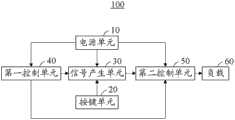
请参阅图2,其为一较佳实施方式的电子设备100的功能模块图。电子设备100可在工作状态和待机状态之间进行切换。电子设备100包括电源单元10、按键单元20、信号产生单元30、第一控制单元40、第二控制单元50及负载60。在本实施方式中,电子设备100为具有待机功能的电子设备。Please refer to FIG. 2 , which is a functional block diagram of an
电源单元10用于给信号产生单元30、第一控制单元40及第二控制单元50提供供电电压。The
按键单元20用于根据用户的按压操作产生唯一对应的按压信号。The
信号产生单元30与按键单元20电性连接。信号产生单元30用于接收按压信号产生第一控制信号并在未接收到按压信号时产生第二控制信号。在本实施方式中,第一控制信号为低电平信号,第二控制信号为高电平。The
第一控制单元40与信号产生单元30及第二控制单元50相连。第一控制单元40用于在电子设备100处于工作状态时控制第二控制单元50与电源单元10之间建立电性连接,并在电子设备100处于待机状态时控制第二控制单元50与电源单元10之间断开电性连接。The
第一控制单元40还用于在第二控制单元50与电源单元10之间已断开电性连接时根据第一控制信号产生切换信号,并根据第二控制信号停止产生切换信号。The
第二控制单元50与信号产生单元30相连。第二控制单元50用于在电子设备100处于工作状态时侦测信号产生单元30的按压信号。第二控制单元50还用于在电子设备100处于待机状态时根据切换信号与电源单元10建立电性连接,从而将将电子设备100切换至工作状态。The
负载60用于根据按压信号执行相应的功能。The
通过使用上述电子设备100可保证电子设备100在待机状态下,通过按压按键单元20稳定地切换至工作状态,并避免了由于第二控制单元50内部封装结构导致电子设备100无法切换至工作状态的情况。By using the
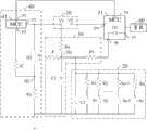
请参阅图3,电源单元10包括第一电压源V1和第二电压源V2。第一电压源V1与第一控制单元40电性连接,并通过信号产生单元30与按键单元20电性连接。第二电压源V2与第二控制单元50电性连接。按键单元20包括多个按键S1~Sn、多个上拉电阻R1~Rn及第二电容C2。多个上拉电阻与多个按键一一对应且串联连接,多个按键的一端通过对应的上拉电阻与信号产生单元30电性连接,另一端接地。Referring to FIG. 3 , the
信号产生单元30包括第一分压电阻Ra、第二分压电阻Rb、第一保护电阻R、第一结点N1及第一电容C1。第一分压电阻Ra连接于第一电压源V1和第一结点N1之间。第二分压电阻Rb连接于第一结点N1和第二控制单元50之间。第一保护电阻R连接于第一结点N1和第一控制单元40之间。第一电容C1连接于第一结点N1和地之间。在本实施方式中,第二分压电阻Rb的阻值远大于第一分压电阻Ra的阻值及多个上拉电阻R1~Rn中任意一个上拉电阻的阻值。The
第一控制单元40包括三极管Q1、第一微控制芯片(Micro Controller Unit,MCU)41、第二结点N2、第三分压电阻Rc及第二保护电阻R’。三极管Q1的基极通过第一保护电阻R与第一结点N1电性连接,发射极与第一电压源V1电性连接,集电极与通过第二结点N2和第三分压电阻Rc接地。第一微控制芯片41包括第一上电引脚P1、第一侦测引脚P2及控制引脚P3。第一上电引脚P1与第一电压源V1电性连接,第一侦测引脚P2通过第二保护电阻R’与第二结点N2电性连接,控制引脚P3与第二控制单元50电性连接。在本实施方式中,三极管Q1为PNP型三极管。The
第二控制单元50包括第二微控制芯片(Micro Controller Unit,MCU) 51。第二微控制芯片51具有第二上电引脚P4、受控引脚P5、第二侦测引脚P6及接地引脚P7。第二上电引脚P4与第二电压源V2电性连接,受控引脚P5与控制引脚P3电性连接,第二侦测引脚P6与第二分压电阻Rb电性连接,接地引脚P7接地。第二微控制芯片51内部封装有二极管D。二极管D正极与受控引脚P5电性连接,负极与接地引脚P7电性连接。The
当电子设备100处于待机状态且未产生按压信号时,第二微控制芯片51断开与第二电压源V2之间的电性连接并停止工作。此时,第一电压源V1、第一分压电阻Ra、第一结点N1、第二分压电阻Rb及二极管D构成放电通路。由于第二分压电阻Rb的阻值远大于第一分压电阻Ra的阻值,第一结点N1的电压近似与第一电压源V1的电压相等。此时,三极管Q1的发射极和基极之间的电压差小于0.7V,三极管Q1截止,第二结点电压为0。此时,第一微控制芯片41停止产生切换信号。When the
当电子设备100处于待机状态且产生按压信号时,被按压的按键与第一结点N1之间形成构成放电通路,与被按压按键串联连接的上拉电阻与第二分压电阻Rb并联,第一结点N1的电压降低。此时,三极管Q1的发射极和基极之间的电压差大于0.7V,三极管Q1导通,第一电压源V1通过第一保护电阻R、第三分压电阻Rc、第一保护电阻R’与第一微控制芯片41构成放电通路,且第二结点电压为第三分压电阻Rc两端的电压。第一微控制芯片41产生第一信号。第二微控制芯片51根据切换信号与第二电压源V2建立电性连接,即第二微控制芯片51上电工作,电子设备100由待机状态切换至工作状态。此时,第二侦测引脚P6根据第一结点N1的电压控制电子设备100执行相应的功能操作。When the
本技术领域的普通技术人员应当认识到,以上的实施方式仅是用来说明本发明,而并非用作为对本发明的限定,只要在本发明的实质精神范围之内,对以上实施例所作的适当改变和变化都落在本发明要求保护的范围之内。Those of ordinary skill in the art should recognize that the above embodiments are only used to illustrate the present invention, rather than to limit the present invention. Alterations and variations are within the scope of the claimed invention.
Claims (10)
Translated fromChinesePriority Applications (3)
| Application Number | Priority Date | Filing Date | Title |
|---|---|---|---|
| CN2012101174514ACN103376748A (en) | 2012-04-20 | 2012-04-20 | Electronic device |
| TW101114749ATW201344409A (en) | 2012-04-20 | 2012-04-25 | Electronic device |
| US13/671,612US20130283077A1 (en) | 2012-04-20 | 2012-11-08 | Wake-up circuit and electronic device |
Applications Claiming Priority (1)
| Application Number | Priority Date | Filing Date | Title |
|---|---|---|---|
| CN2012101174514ACN103376748A (en) | 2012-04-20 | 2012-04-20 | Electronic device |
Publications (1)
| Publication Number | Publication Date |
|---|---|
| CN103376748Atrue CN103376748A (en) | 2013-10-30 |
Family
ID=49381283
Family Applications (1)
| Application Number | Title | Priority Date | Filing Date |
|---|---|---|---|
| CN2012101174514APendingCN103376748A (en) | 2012-04-20 | 2012-04-20 | Electronic device |
Country Status (3)
| Country | Link |
|---|---|
| US (1) | US20130283077A1 (en) |
| CN (1) | CN103376748A (en) |
| TW (1) | TW201344409A (en) |
Families Citing this family (5)
| Publication number | Priority date | Publication date | Assignee | Title |
|---|---|---|---|---|
| CN103376753A (en)* | 2012-04-28 | 2013-10-30 | 鸿富锦精密工业(深圳)有限公司 | Standby wake-up circuit and electronic device |
| TWI577364B (en)* | 2015-05-22 | 2017-04-11 | 台達電子工業股份有限公司 | Control system applied to power device and control method thereof |
| EP3665963B1 (en)* | 2017-08-11 | 2022-02-23 | Apple Inc. | Wake up signaling in wireless telecommunication networks |
| CN111934666B (en)* | 2020-06-18 | 2023-07-28 | 惠州市德赛西威汽车电子股份有限公司 | Key circuit with system wake-up function |
| CN117458833B (en)* | 2023-12-26 | 2024-04-19 | 无锡梵克罗电气设计有限公司 | A battery-powered inverter low-power startup wake-up circuit and inverter |
Family Cites Families (1)
| Publication number | Priority date | Publication date | Assignee | Title |
|---|---|---|---|---|
| US8595529B2 (en)* | 2010-12-16 | 2013-11-26 | Qualcomm Incorporated | Efficient power management and optimized event notification in multi-processor computing devices |
- 2012
- 2012-04-20CNCN2012101174514Apatent/CN103376748A/enactivePending
- 2012-04-25TWTW101114749Apatent/TW201344409A/enunknown
- 2012-11-08USUS13/671,612patent/US20130283077A1/ennot_activeAbandoned
Also Published As
| Publication number | Publication date |
|---|---|
| US20130283077A1 (en) | 2013-10-24 |
| TW201344409A (en) | 2013-11-01 |
Similar Documents
| Publication | Publication Date | Title |
|---|---|---|
| US8218279B2 (en) | Electronic device and method for dynamic USB power assignment | |
| CN103683348B (en) | There is the electronic installation of power consumption detecting function | |
| CN109494120B (en) | Relay control circuit | |
| US20140085756A1 (en) | Protection circuit and electronic device using the same | |
| US20120274390A1 (en) | Power supply circuit | |
| CN107589340B (en) | Load insertion detection circuit, plug-in port and electric appliance | |
| CN103376748A (en) | Electronic device | |
| US8493701B2 (en) | Overvoltage protection circuit | |
| US20130162222A1 (en) | Charging control circuit | |
| CN103997334A (en) | Level shift circuit | |
| CN204376697U (en) | The circuit of electric equipment and reduction Switching Power Supply stand-by power consumption | |
| CN103336165A (en) | Detection circuit for overcurrent of alternating current and direct current | |
| CN202495920U (en) | Reset circuit and set-top box having the circuit | |
| TWI556540B (en) | Electronic device power supply system | |
| US9374079B2 (en) | Level jump reset IC design circuit | |
| US8767365B2 (en) | Protection circuit | |
| TW201826709A (en) | Reset circuit and electronic equipment | |
| US20140339921A1 (en) | Light Load Current Detection System | |
| TWI540419B (en) | Electronic device | |
| CN104656724B (en) | Electronic installation | |
| US20110235219A1 (en) | Protecting device | |
| CN209515563U (en) | Relay control circuit | |
| CN102736524A (en) | Power switch | |
| CN105572603B (en) | Power management system and detection device of power module thereof | |
| TWI547031B (en) | Electrical contact detection circuit and portable electrical system using the same |
Legal Events
| Date | Code | Title | Description |
|---|---|---|---|
| C06 | Publication | ||
| PB01 | Publication | ||
| C02 | Deemed withdrawal of patent application after publication (patent law 2001) | ||
| WD01 | Invention patent application deemed withdrawn after publication | Application publication date:20131030 |