CN103367584A - Light emitting diode and optical element - Google Patents
Light emitting diode and optical elementDownload PDFInfo
- Publication number
- CN103367584A CN103367584ACN2012100890714ACN201210089071ACN103367584ACN 103367584 ACN103367584 ACN 103367584ACN 2012100890714 ACN2012100890714 ACN 2012100890714ACN 201210089071 ACN201210089071 ACN 201210089071ACN 103367584 ACN103367584 ACN 103367584A
- Authority
- CN
- China
- Prior art keywords
- semiconductor layer
- emitting diode
- layer
- nano
- light
- Prior art date
- Legal status (The legal status is an assumption and is not a legal conclusion. Google has not performed a legal analysis and makes no representation as to the accuracy of the status listed.)
- Granted
Links
Images


Classifications
- G—PHYSICS
- G02—OPTICS
- G02B—OPTICAL ELEMENTS, SYSTEMS OR APPARATUS
- G02B19/00—Condensers, e.g. light collectors or similar non-imaging optics
- G02B19/0033—Condensers, e.g. light collectors or similar non-imaging optics characterised by the use
- G02B19/0047—Condensers, e.g. light collectors or similar non-imaging optics characterised by the use for use with a light source
- G02B19/0061—Condensers, e.g. light collectors or similar non-imaging optics characterised by the use for use with a light source the light source comprising a LED
- H—ELECTRICITY
- H10—SEMICONDUCTOR DEVICES; ELECTRIC SOLID-STATE DEVICES NOT OTHERWISE PROVIDED FOR
- H10H—INORGANIC LIGHT-EMITTING SEMICONDUCTOR DEVICES HAVING POTENTIAL BARRIERS
- H10H20/00—Individual inorganic light-emitting semiconductor devices having potential barriers, e.g. light-emitting diodes [LED]
- H10H20/80—Constructional details
- H10H20/81—Bodies
- H10H20/819—Bodies characterised by their shape, e.g. curved or truncated substrates
- H—ELECTRICITY
- H10—SEMICONDUCTOR DEVICES; ELECTRIC SOLID-STATE DEVICES NOT OTHERWISE PROVIDED FOR
- H10H—INORGANIC LIGHT-EMITTING SEMICONDUCTOR DEVICES HAVING POTENTIAL BARRIERS
- H10H20/00—Individual inorganic light-emitting semiconductor devices having potential barriers, e.g. light-emitting diodes [LED]
- H10H20/80—Constructional details
- H10H20/85—Packages
- H10H20/855—Optical field-shaping means, e.g. lenses
- B—PERFORMING OPERATIONS; TRANSPORTING
- B82—NANOTECHNOLOGY
- B82Y—SPECIFIC USES OR APPLICATIONS OF NANOSTRUCTURES; MEASUREMENT OR ANALYSIS OF NANOSTRUCTURES; MANUFACTURE OR TREATMENT OF NANOSTRUCTURES
- B82Y20/00—Nanooptics, e.g. quantum optics or photonic crystals
- H—ELECTRICITY
- H10—SEMICONDUCTOR DEVICES; ELECTRIC SOLID-STATE DEVICES NOT OTHERWISE PROVIDED FOR
- H10H—INORGANIC LIGHT-EMITTING SEMICONDUCTOR DEVICES HAVING POTENTIAL BARRIERS
- H10H20/00—Individual inorganic light-emitting semiconductor devices having potential barriers, e.g. light-emitting diodes [LED]
- H10H20/80—Constructional details
- H10H20/81—Bodies
- H10H20/819—Bodies characterised by their shape, e.g. curved or truncated substrates
- H10H20/82—Roughened surfaces, e.g. at the interface between epitaxial layers
- H—ELECTRICITY
- H10—SEMICONDUCTOR DEVICES; ELECTRIC SOLID-STATE DEVICES NOT OTHERWISE PROVIDED FOR
- H10H—INORGANIC LIGHT-EMITTING SEMICONDUCTOR DEVICES HAVING POTENTIAL BARRIERS
- H10H20/00—Individual inorganic light-emitting semiconductor devices having potential barriers, e.g. light-emitting diodes [LED]
- H10H20/80—Constructional details
- H10H20/83—Electrodes
- H—ELECTRICITY
- H10—SEMICONDUCTOR DEVICES; ELECTRIC SOLID-STATE DEVICES NOT OTHERWISE PROVIDED FOR
- H10H—INORGANIC LIGHT-EMITTING SEMICONDUCTOR DEVICES HAVING POTENTIAL BARRIERS
- H10H20/00—Individual inorganic light-emitting semiconductor devices having potential barriers, e.g. light-emitting diodes [LED]
- H10H20/80—Constructional details
- H10H20/872—Periodic patterns for optical field-shaping, e.g. photonic bandgap structures
- Y—GENERAL TAGGING OF NEW TECHNOLOGICAL DEVELOPMENTS; GENERAL TAGGING OF CROSS-SECTIONAL TECHNOLOGIES SPANNING OVER SEVERAL SECTIONS OF THE IPC; TECHNICAL SUBJECTS COVERED BY FORMER USPC CROSS-REFERENCE ART COLLECTIONS [XRACs] AND DIGESTS
- Y10—TECHNICAL SUBJECTS COVERED BY FORMER USPC
- Y10S—TECHNICAL SUBJECTS COVERED BY FORMER USPC CROSS-REFERENCE ART COLLECTIONS [XRACs] AND DIGESTS
- Y10S977/00—Nanotechnology
- Y10S977/70—Nanostructure
- Y—GENERAL TAGGING OF NEW TECHNOLOGICAL DEVELOPMENTS; GENERAL TAGGING OF CROSS-SECTIONAL TECHNOLOGIES SPANNING OVER SEVERAL SECTIONS OF THE IPC; TECHNICAL SUBJECTS COVERED BY FORMER USPC CROSS-REFERENCE ART COLLECTIONS [XRACs] AND DIGESTS
- Y10—TECHNICAL SUBJECTS COVERED BY FORMER USPC
- Y10S—TECHNICAL SUBJECTS COVERED BY FORMER USPC CROSS-REFERENCE ART COLLECTIONS [XRACs] AND DIGESTS
- Y10S977/00—Nanotechnology
- Y10S977/902—Specified use of nanostructure
- Y10S977/932—Specified use of nanostructure for electronic or optoelectronic application
Landscapes
- Physics & Mathematics (AREA)
- General Physics & Mathematics (AREA)
- Optics & Photonics (AREA)
- Led Devices (AREA)
Abstract
Translated fromChineseDescription
Translated fromChinese技术领域technical field
本发明涉及一种发光二极管及光学元件,尤其涉及一种具有三维纳米结构阵列的发光二极管及光学元件。The invention relates to a light-emitting diode and an optical element, in particular to a light-emitting diode and an optical element with a three-dimensional nanostructure array.
背景技术Background technique
由氮化镓半导体材料制成的高效蓝光线、绿光线和白光线发光二极管具有寿命长、节能、绿色环保等显著特点,已被广泛应用于大屏幕彩色显示、汽车照明、交通信号、多媒体显示和光线通讯等领域,特别是在照明领域具有广阔的发展潜力。High-efficiency blue, green and white light-emitting diodes made of gallium nitride semiconductor materials have the characteristics of long life, energy saving, and environmental protection. They have been widely used in large-screen color displays, automotive lighting, traffic signals, and multimedia displays. And light communication and other fields, especially in the field of lighting has broad development potential.
传统的发光二极管通常包括N型半导体层、P型半导体层、设置在N型半导体层与P型半导体层之间的活性层、设置在P型半导体层上的P型电极(通常为透明电极)以及设置在N型半导体层上的N型电极。发光二极管处于工作状态时,在P型半导体层与N型半导体层上分别施加正、负电压,这样,存在于P型半导体层中的空穴与存在于N型半导体层中的电子在活性层中发生复合而产生光子,且光子从发光二极管中射出。A traditional light-emitting diode usually includes an N-type semiconductor layer, a P-type semiconductor layer, an active layer disposed between the N-type semiconductor layer and the P-type semiconductor layer, and a P-type electrode (usually a transparent electrode) disposed on the P-type semiconductor layer. and an N-type electrode disposed on the N-type semiconductor layer. When the light-emitting diode is in the working state, positive and negative voltages are applied to the P-type semiconductor layer and the N-type semiconductor layer respectively, so that the holes existing in the P-type semiconductor layer and the electrons existing in the N-type semiconductor layer are in the active layer. Recombination occurs in the light emitting diode to generate photons, and the photons are emitted from the light emitting diode.
然而,现有的发光二极管的发光效率不够高,部分原因是由于来自活性层的大角度光线(角度大于23.58°临界角的光线)在N型或P型半导体与空气的界面处发生全反射,从而大部分大角度光线被限制在发光二极管的内部,直至以热等方式耗散,这对发光二极管而言非常不利。However, the luminous efficiency of existing light-emitting diodes is not high enough, partly due to the total reflection of large-angle light rays (light rays with angles greater than 23.58° critical angle) from the active layer at the interface between N-type or P-type semiconductors and air, Therefore, most of the large-angle light is confined inside the light-emitting diode until it is dissipated by means of heat, which is very unfavorable for the light-emitting diode.
发明内容Contents of the invention
有鉴于此,确有必要提供一发光效率较高的发光二极管及光学元件。In view of this, it is indeed necessary to provide a light emitting diode and an optical element with higher luminous efficiency.
一种发光二极管,包括:一基底,所述基底包括一外延生长面;一第一半导体层、一活性层以及一第二半导体层,该第一半导体层、活性层以及第二半导体层依次层叠设置于所述基底的外延生长面,所述第二半导体层远离活性层的表面为所述发光二极管的出光面;一第一电极,该第一电极与所述第一半导体层电连接;一第二电极,该第二电极与所述第二半导体层电连接;其中,所述第二半导体层远离活性层的表面具有多个第一三维纳米结构,所述第一三维纳米结构为间隔设置的条形凸起结构,所述条形凸起结构的横截面为弓形。A light emitting diode, comprising: a base, the base includes an epitaxial growth surface; a first semiconductor layer, an active layer and a second semiconductor layer, the first semiconductor layer, the active layer and the second semiconductor layer are sequentially stacked Set on the epitaxial growth surface of the substrate, the surface of the second semiconductor layer away from the active layer is the light emitting surface of the light emitting diode; a first electrode, the first electrode is electrically connected to the first semiconductor layer; a The second electrode is electrically connected to the second semiconductor layer; wherein, the surface of the second semiconductor layer away from the active layer has a plurality of first three-dimensional nanostructures, and the first three-dimensional nanostructures are arranged at intervals The strip-shaped convex structure, the cross-section of the strip-shaped convex structure is arcuate.
一种发光二极管,其包括:一基底,所述基底包括一外延生长面;一有源层设置于所述基底的外延生长面;其中,所述有源层远离基底的表面具有多个第一三维纳米结构,该第一三维纳米结构为间隔设置的条形凸起结构,所述条形凸起结构的横截面为弓形。A light-emitting diode, which includes: a base, the base includes an epitaxial growth surface; an active layer is arranged on the epitaxial growth surface of the base; wherein, the surface of the active layer away from the base has a plurality of first A three-dimensional nanostructure, the first three-dimensional nanostructure is a strip-shaped protrusion structure arranged at intervals, and the cross-section of the strip-shaped protrusion structure is arcuate.
一种光学元件,其包括:一本体以及多个第一三维纳米结构,所述第一三维纳米结构设置于所述本体的表面,其中,该第一三维纳米结构为间隔设置的条形凸起结构,所述条形凸起结构的横截面为弓形。An optical element, comprising: a body and a plurality of first three-dimensional nanostructures, the first three-dimensional nanostructures are arranged on the surface of the body, wherein the first three-dimensional nanostructures are strip-shaped protrusions arranged at intervals structure, the cross-section of the strip-shaped convex structure is arcuate.
与现有技术相比较,本发明的发光二极管中,由于所述发光二极管的出光面具有多个弓形的三维纳米结构,当所述活性层中产生的入射角大于临界角的大角度光线并入射至所述三维纳米结构时,该大角度光线通过所述三维纳米结构的弓形表面而转变为小角度光线,若小角度光线小于临界角,那么,该小角度光线可以射出。也就是说,光线入射至形成有多个三维纳米结构的表面时,与光线入射至平面结构相比,入射角大于临界角的某一范围的光线也会从发光二极管的出光面出射,进而可以提高发光二极管的出光效率。Compared with the prior art, in the light-emitting diode of the present invention, since the light-emitting surface of the light-emitting diode has multiple bow-shaped three-dimensional nanostructures, when the large-angle light with an incident angle greater than the critical angle generated in the active layer is incident When reaching the three-dimensional nanostructure, the high-angle light passes through the arcuate surface of the three-dimensional nanostructure and is transformed into a small-angle light. If the small-angle light is smaller than the critical angle, the small-angle light can be emitted. That is to say, when light is incident on a surface formed with multiple three-dimensional nanostructures, compared with light incident on a planar structure, light in a certain range with an incident angle greater than the critical angle will also exit from the light-emitting surface of the light-emitting diode, and then can Improve the light extraction efficiency of the light emitting diode.
附图说明Description of drawings
图1为本发明第一实施例提供的发光二极管的结构示意图。FIG. 1 is a schematic structural diagram of a light emitting diode provided by the first embodiment of the present invention.
图2为本发明第一实施例提供的发光二极管中第二半导体层的结构示意图。FIG. 2 is a schematic structural diagram of the second semiconductor layer in the light emitting diode provided by the first embodiment of the present invention.
图3为本发明第一实施例提供的发光二极管中第二半导体层的扫描电镜照片。FIG. 3 is a scanning electron micrograph of the second semiconductor layer in the light emitting diode provided by the first embodiment of the present invention.
图4为本发明第一实施例提供的发光二极管中第二半导体层的出光原理图。FIG. 4 is a schematic diagram of the light extraction principle of the second semiconductor layer in the light emitting diode provided by the first embodiment of the present invention.
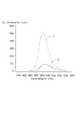
图5为本发明第一实施例提供的发光二极管与标准发光二极管的发光强度对比曲线。Fig. 5 is a comparison curve of the luminous intensity of the light emitting diode provided by the first embodiment of the present invention and the standard light emitting diode.
图6为本发明第一实施例提供的发光二极管的制备方法的工艺流程图。FIG. 6 is a process flow diagram of the method for manufacturing a light emitting diode provided in the first embodiment of the present invention.
图7为本发明第一实施例提供的发光二极管的制备方法中在第二半导体层表面形成多个第一三维纳米结构的制备方法的工艺流程图。FIG. 7 is a process flow chart of a method for forming a plurality of first three-dimensional nanostructures on the surface of a second semiconductor layer in the method for manufacturing a light emitting diode according to the first embodiment of the present invention.
图8为本发明第一实施例提供的发光二极管的制备方法中刻蚀第二半导体层表面的制备方法的示意图。FIG. 8 is a schematic diagram of a preparation method of etching the surface of the second semiconductor layer in the preparation method of the light emitting diode provided in the first embodiment of the present invention.
图9为本发明第二实施例提供的发光二极管的结构示意图。FIG. 9 is a schematic structural diagram of a light emitting diode provided by the second embodiment of the present invention.
图10为本发明第二实施例提供的发光二极管的制备方法的工艺流程图。FIG. 10 is a process flow chart of a method for manufacturing a light emitting diode provided in the second embodiment of the present invention.
主要元件符号说明Description of main component symbols
如下具体实施方式将结合上述附图进一步说明本发明。The following specific embodiments will further illustrate the present invention in conjunction with the above-mentioned drawings.
具体实施方式Detailed ways
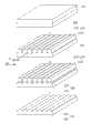
请参阅图1,本发明第一实施例提供一种发光二极管10,包括:一基底100、一第一半导体层110、一活性层120、一第二半导体层130、一第一电极140以及一第二电极150。所述第一半导体层110、活性层120以及第二半导体层130依次层叠设置于基底100的表面,所述第一半导体层110与所述基底100接触设置。所述第二半导体层130远离活性层120的表面为所述发光二极管10的出光面,所述第一电极140与所述第一半导体层110电连接。所述第二电极150与所述第二半导体层130电连接。所述发光二极管10的出光面具有多个第一三维纳米结构134。Please refer to FIG. 1, the first embodiment of the present invention provides a light emitting diode 10, including: a
所述基底100主要起支撑作用,该基底100具有一支持外延生长的外延生长面。所述基底100的厚度为300至500微米,所述基底100的材料可以为SOI(silicon on insulator,绝缘基底上的硅)、LiGaO2、LiAlO2、Al2O3、Si、GaAs、GaN、GaSb、InN、InP、InAs、InSb、AlP、AlAs、AlSb、AlN、GaP、SiC、SiGe、GaMnAs、GaAlAs、GaInAs、GaAlN、GaInN、AlInN、GaAsP、InGaN、AlGaInN、AlGaInP、GaP:Zn或GaP:N等。所述基底100的材料可根据所述需要生长的半导体层的材料进行选择,所述基底100的材料与所述半导体层的材料具有较小的晶格失配及相近的热膨胀系数,从而可以减少生长的半导体层中的晶格缺陷,提高其质量。本实施例中,所述基底100的厚度为400微米,其材料为蓝宝石。The
所述第一半导体层110设置于所述基底100的外延生长面。所述第一半导体层110、第二半导体层130分别为N型半导体层和P型半导体层两种类型中的一种。具体地,当该第一半导体层110为N型半导体层时,第二半导体层130为P型半导体层;当该第一半导体层110为P型半导体层时,第二半导体层130为N型半导体层。所述N型半导体层起到提供电子的作用,所述P型半导体层起到提供空穴的作用。N型半导体层的材料包括N型氮化镓、N型砷化镓及N型磷化铜等材料中的一种或几种。P型半导体层的材料包括P型氮化镓、P型砷化镓及P型磷化铜等材料中的一种或几种。所述第一半导体层110的厚度为1微米至5微米。本实施例中,第一半导体层110的材料为N型氮化镓。可选择地,一缓冲层(图未示)可以设置于基底100和第一半导体层110之间,并与基底100和第一半导体层110分别接触,此时第一半导体层110靠近基底100的表面与缓冲层接触。所述缓冲层有利于提高所述第一半导体层110的外延生长质量,减少晶格缺陷。所述缓冲层的厚度为10纳米至300纳米,其材料可以为氮化镓或氮化铝等。The
本实施例中,所述第一半导体层110具有相对的第一表面(未标示)及第二表面(未标示),所述第一表面与所述基底100相接触,所述第二表面为第一半导体层110远离基底100的表面。所述第二表面按其功能可区分为一第一区域(未标示)及第二区域(未标示),其中所述第一区域用于设置所述活性层120,所述第二区域用于设置所述第一电极140。In this embodiment, the
所述活性层120设置于所述第一半导体层110的第一区域。优选地,所述活性层120和第一半导体层110的接触面积与第一区域的面积相等。即所述活性层120完全覆盖所述第一半导体层110的第一区域。所述活性层120为包含一层或多层量子阱层的量子阱结构(Quantum Well)。所述活性层120用于提供光子。所述活性层120的材料为氮化镓、氮化铟镓、氮化铟镓铝、砷化稼、砷化铝稼、磷化铟镓、磷化铟砷或砷化铟镓中的一种或几种,其厚度为0.01微米至0.6微米。本实施例中,所述活性层120为两层结构,包括一氮化铟镓层及一氮化镓层,其厚度约为0.03微米。The
所述第二半导体层130设置于所述活性层120远离基底100的表面,具体的,所述第二半导体层130覆盖所述活性层120远离基底100的整个表面。所述第二半导体层130的厚度为0.1微米~3微米。所述第二半导体层130可为N型半导体层或P型半导体层两种类型,并且所述第二半导体层130与第一半导体层110分属两种不同类型的半导体层。所述第二半导体层130远离基底100的表面作为发光二极管10的出光面。本实施例中,所述第二半导体层130为镁(Mg)掺杂的P型氮化镓,其厚度为0.3微米。The
请一并参阅图2及图3,所述第二半导体层130包括一本体132以及多个第一三维纳米结构134,所述多个第一三维纳米结构134设置于所述本体132远离活性层120的表面。所述多个第一三维纳米结构134可以以阵列的形式分布。所述阵列形式分布指所述多个第一三维纳米结构134可以按照等间距排布、同心圆环排布或同心回形排布,形成所述第二半导体层130图案化的表面。即,所述发光二极管10的出光面为所述多个第一三维纳米结构134形成的图案化表面。所述相邻的两个第一三维纳米结构134之间的距离D1相等,为10纳米~1000纳米,优选为100纳米~200纳米。本实施例中,所述多个第一三维纳米结构134以等间距排列,且相邻两个第一三维纳米结构134之间的距离约为140纳米。Please refer to FIG. 2 and FIG. 3 together. The
所述第一三维纳米结构134为条形凸起结构,所述条形凸起结构为从所述第二半导体层130的本体132向外延伸出的条形凸起实体。所述第一三维纳米结构134以直线、折线或曲线并排延伸。所述第一三维纳米结构134与所述第二半导体层130的本体132为一体成型结构。所述多个第一三维纳米结构134的延伸方向相同。所述第一三维纳米结构134的横截面为弓形。所述弓形的高度H为100纳米~500纳米,优选为150纳米~200纳米;所述弓形的宽度D2为200纳米~1000纳米,优选为300纳米~400纳米。更优选地,所述第一三维纳米结构134的横截面为半圆形,其半径为150纳米~200纳米。本实施例中,所述第一三维纳米结构134的横截面为半圆形,且该半圆形的半径约为160纳米,即,H=1/2 D2=160纳米。The first three-
所述第一电极140与所述第一半导体层110电连接。本实施例中,所述第一电极140设置于所述第一半导体层110的第二区域,并覆盖该第二区域的部分表面。所述第一电极140与所述活性层120间隔设置。所述第一电极140可以为N型电极或P型电极,其与第一半导体层110的类型相同。所述第一电极140至少为一层的结构,其材料为钛、银、铝、镍、金或其任意组合。本实施例中,所述第一电极140为两层结构,一层为厚度15纳米的钛,另一层为厚度200纳米的金。The
所述第二电极150的类型可以为N型电极或P型电极,其与第二半导体层130的类型相同。所述第二电极150的形状不限,可根据实际需要进行选择。所述第二电极150至少为一层结构,其材料为钛、银、铝、镍、金或其任意组合,也可为ITO或碳纳米管膜。本实施例中,所述第二电极150为P型电极。所述第二电极150为两层结构,一层为厚度为15纳米的钛,另一层为厚度为100纳米的金,形成一钛/金电极。The type of the
进一步的,可在基底100远离活性层120的表面设置一反射层(图未示),所述反射层的材料可为钛、银、铝、镍、金或其任意组合。当活性层中产生的光子到达该反射层后,所述反射层可将光子反射,从而使之从所述发光二极管10的出光面射出,进而可进一步提高所述发光二极管10的出光效率。Further, a reflection layer (not shown) may be provided on the surface of the
请一并参阅图4,本发明第一实施例提供的发光二极管10,由于所述发光二极管10的出光面形成有多个第一三维纳米结构134,从而形成一图案化的表面。当所述活性层120中产生的入射角大于临界角α(23.58°)的大角度光线入射至所述第一三维纳米结构134时,该大角度光线通过所述第一三维纳米结构134的弓形表面或半圆形表面而转变为入射角为β的小角度光线,若入射角β小于临界角α,那么,该小角度光线可以射出。也就是说,光线入射至形成有多个第一三维纳米结构134的表面时,与光线入射至平面结构相比,入射角大于临界角α的某一范围的光线也会从发光二极管10的出光面出射,进而可以提高发光二极管的出光效率。请参阅图5,本发明第一实施例提供的发光二极管10的发光强度(曲线I)可达到标准发光二极管的发光强度(曲线II)的4.7倍,从而大大其高了该发光二极管10的发光效率。Please also refer to FIG. 4 . In the light emitting diode 10 provided by the first embodiment of the present invention, a plurality of first three-
请参阅图6,本发明进一步提供所述发光二极管10的制备方法,该制备方法具体包括以下步骤:Please refer to FIG. 6 , the present invention further provides a preparation method of the light emitting diode 10, the preparation method specifically includes the following steps:
步骤S11,提供一基底100,所述基底100具有一外延生长面;Step S11, providing a
步骤S12,在所述外延生长面依次生长一第一半导体层110、一活性层120及一第二半导体预制层160;Step S12, growing a
步骤S13,设置一第一电极140,使其与所述第一半导体层110电连接;Step S13, setting a
步骤S14,设置一第二电极150,使其与所述第二半导体预制层160电连接;Step S14, setting a
步骤S15,刻蚀所述第二半导体预制层160远离活性层120的表面,形成多个第一三维纳米结构134。Step S15 , etching the surface of the second semiconductor prefabricated
在步骤S11中,所述基底100具有一提供所述第一半导体层110生长的外延生长面。所述基底100的外延生长面是分子平滑的表面,且去除了氧或碳等杂质。所述基底100可以为单层或多层结构。当所述基底100为单层结构时,该基底100可以为一单晶结构体,且具有一晶面作为第一半导体层110的外延生长面。当所述基底100为多层结构时,其需要包括至少一层所述单晶结构体,且该单晶结构体具有一晶面作为第一半导体层110的外延生长面。所述基底100的材料可以根据所要生长的第一半导体层110来选择,优选地,所述基底100与第一半导体层110具有相近的晶格常数以及热膨胀系数。所述基底100的厚度、大小和形状不限,可以根据实际需要选择。所述基底100不限于所述列举的材料,只要具有支持第一半导体层110生长的外延生长面的基底100均属于本发明的保护范围。本实施例中,所述基底100的厚度为400微米,其材料为蓝宝石。In step S11 , the
在步骤S12中,所述第一半导体层110的生长方法可以通过分子束外延法(MBE)、化学束外延法(CBE)、减压外延法、低温外延法、选择外延法、液相沉积外延法(LPE)、金属有机气相外延法(MOVPE)、超真空化学气相沉积法(UHVCVD)、氢化物气相外延法(HVPE)、以及金属有机化学气相沉积法(MOCVD)等中的一种或多种实现。In step S12, the growth method of the
本实施例中,所述第一半导体层110为Si掺杂的N型氮化镓。本实施例采用MOCVD工艺制备所述第一半导体层110,所述第一半导体层110的生长为异质外延生长。其中,采用高纯氨气(NH3)作为氮的源气,采用氢气(H2)作载气,采用三甲基镓(TMGa)或三乙基镓(TEGa)作为Ga源,采用硅烷(SiH4)作为Si源。所述第一半导体层110的生长具体包括以下步骤:In this embodiment, the
步骤(a1),将基底100置入一反应室,加热到1100oC~1200oC,并通入H2、N2或其混合气体作为载气,高温烘烤200秒~1000秒。In step (a1), the
步骤(a2),继续通入载气,并降温到500oC~650oC,通入三甲基镓或三乙基镓,并同时通入氨气,低温生长GaN层,所述低温GaN层作为继续生长第一半导体层110的缓冲层。由于第一半导体层110与蓝宝石基底100之间具有不同的晶格常数,因此,采用一缓冲层来减少第一半导体层110生长过程中的晶格失配,降低生长的第一半导体层110的位错密度。Step (a2), continue to feed the carrier gas, and lower the temperature to 500oC~650oC, feed trimethylgallium or triethylgallium, and feed ammonia gas at the same time, grow the GaN layer at a low temperature, and the low-temperature GaN layer is used as a continuous growth The buffer layer of the
步骤(a3),停止通入三甲基镓或三乙基镓,继续通入氨气和载气,同时将温度升高到1100oC~1200oC,并恒温保持30秒~300秒。In step (a3), stop feeding trimethylgallium or triethylgallium, continue feeding ammonia gas and carrier gas, and raise the temperature to 1100oC~1200oC at the same time, and keep the constant temperature for 30 seconds~300 seconds.
步骤(a4),将所述基底100的温度保持在1000oC~1100oC,同时重新通入三甲基镓及硅烷,或三乙基镓及硅烷,在高温下生长出高质量的第一半导体层110。In step (a4), the temperature of the
进一步的,在步骤(a4)之后,可将基底100的温度保持在1000oC~1100oC,重新通入三甲基镓或三乙基镓一定时间,生长一未掺杂的半导体层,然后再通入硅烷,继续生长第一半导体层110。该未掺杂的半导体层可进一步减小生长所述第一半导体层110的晶格缺陷。Further, after step (a4), the temperature of the
所述活性层120的生长方法与第一半导体层110基本相同。具体的,采用三甲基铟作为铟源,生长所述活性层120,所述活性层120的生长包括以下步骤:The growth method of the
步骤(b1),向反应室内通入氨气、氢气及Ga源气体,将反应室的温度保持在700oC~900oC,使反应室压强保持在50托~500托;Step (b1), feeding ammonia gas, hydrogen gas and Ga source gas into the reaction chamber, maintaining the temperature of the reaction chamber at 700°C to 900°C, and maintaining the pressure of the reaction chamber at 50 torr to 500 torr;
步骤(b2),向反应室通入三甲基铟,生长InGaN/GaN多量子阱层,在所述第一半导体层110表面形成所述活性层120。Step (b2), injecting trimethylindium into the reaction chamber to grow an InGaN/GaN multiple quantum well layer, and forming the
所述第二半导体预制层160的生长方法与第一半导体层110基本相同,具体的,在生长完活性层120之后,采用二茂镁作(Cp2Mg)为镁源,所述第二半导体预制层160的生长包括以下步骤:The growth method of the second semiconductor prefabricated
步骤(c1),停止通入三甲基铟,将反应室的温度保持在1000oC~1100oC,使反应室压强保持在76托~200托;Step (c1), stop feeding trimethylindium, keep the temperature of the reaction chamber at 1000oC~1100oC, keep the pressure of the reaction chamber at 76 Torr~200 Torr;
步骤(c2),向反应室通入二茂镁,生长Mg掺杂的P型GaN层,形成所述第二半导体预制层160。In step (c2), magnesocene is introduced into the reaction chamber to grow a Mg-doped P-type GaN layer to form the second semiconductor prefabricated
在步骤S13中,所述第一电极140的设置方法具体包括以下步骤:In step S13, the setting method of the
步骤S131,刻蚀部分第二半导体预制层160及活性层120,暴露出所述第一半导体层110的部分表面;Step S131, etching part of the second semiconductor prefabricated
步骤S132,在暴露出来的第一半导体层110的表面设置一第一电极140。Step S132 , disposing a
在步骤S131中,所述第二半导体预制层160及所述活性层120可通过光刻蚀、电子刻蚀、等离子刻蚀以及化学腐蚀等方法进行刻蚀,从而暴露所述第一半导体层110的部分表面,进而形成所述第一半导体层110的第二区域。In step S131, the second semiconductor prefabricated
在步骤S132中,所述第一电极140可通过电子束蒸发法、真空蒸镀法及离子溅射法等方法制备。进一步的,可将一导电基底通过导电胶等方式贴附于所述第一半导体层110暴露的部分表面形成所述第一电极140。本实施例中,所述第一电极140设置于所述第一半导体层110的第二区域,并且与所述活性层120及第二半导体预制层160间隔设置。In step S132, the
在步骤S14中,所述第二电极150的制备方法与第一电极140的制备方法相同。本实施例中,采用电子束蒸发法制备所述第二电极150。所述第二电极150设置于所述第二半导体预制层160的部分表面,即设置于所述发光二极管20的出光面。所述第二电极150基本不影响所述发光二极管10的出光率。In step S14 , the preparation method of the
请一并参阅图7,在步骤S15中,在所述第二半导体预制层160表面形成多个第一三维纳米结构134具体包括以下步骤:Please refer to FIG. 7 together. In step S15, forming a plurality of first three-
步骤S151,在所述第二半导体预制层160的表面设置一掩膜层170;Step S151, setting a
步骤S152,刻蚀所述掩膜层170,使所述掩膜层170图案化;Step S152, etching the
步骤S153,刻蚀所述第二半导体预制层160,使所述第二半导体预制层160的表面图案化,形成多个第一三维纳米结构134;Step S153, etching the second semiconductor prefabricated
步骤S154,去除所述掩膜层170,从而形成所述第二半导体层130。Step S154 , removing the
在步骤151中,所述掩膜层170的材料可以为ZEP520A、HSQ(hydrogen silsesquioxane)、PMMA(Polymethylmethacrylate)、PS(Polystyrene)、SOG(Silicon on glass)或其他有机硅类低聚物等材料。所述掩膜层170用于保护其覆盖位置处的第二半导体预制层160。本实施例中,所述掩膜层170的材料为ZEP520A。可以理解,为了保护第一电极140及第二电极150,也需要将所述第一电极140及第二电极150的表面通过所述掩膜层170覆盖。In step 151, the material of the
所述掩膜层170可以利用旋转涂布(Spin Coat)、裂缝涂布(Slit Coat)、裂缝旋转涂布(Slit and Spin Coat)或者干膜涂布法(Dry Film Lamination)的任一种将掩膜层170的材料涂布于第二半导体预制层160、第一电极140及第二电极150远离基底100的表面。具体的,首先,清洗所述第二半导体预制层160、第一电极140及第二电极150远离基底100的表面;其次,在所述第二半导体预制层160、第一电极140及第二电极150远离基底100的表面旋涂ZEP520,旋涂转速为500转/分钟~6000转/分钟,时间为0.5分钟~1.5分钟;其次,在140oC~180oC温度下烘烤3~5分钟,从而在所述第二半导体预制层160、第一电极140及第二电极150远离基底100的表面形成该掩膜层170。该掩膜层170的厚度为100纳米~500纳米。The
在步骤S152中,所述使掩膜层170图案化的方法包括:电子束曝光法(electron beam lithography,EBL)、光刻法以及纳米压印法等。本实施例中,电子束曝光法。具体地,通过电子束曝光法使所述掩膜层170形成多个沟槽172,从而使所述沟槽172对应区域的第二半导体预制层160的表面暴露出来。在所述图案化掩膜层170中,相邻两个沟槽172之间的掩膜层170形成一挡墙174,且每一挡墙174与每一第一三维纳米结构134一一对应。具体地,所述挡墙174的分布方式与所述第一三维纳米结构134的分布方式一致;所述挡墙174的宽度等于所述第一三维纳米结构134的宽度,即D2;且相邻两个挡墙174之间的间距等于相邻两个第一三维纳米结构134之间的间距,即D1。本实施例中,所述挡墙174以等间距排列,每一挡墙174的宽度为320纳米,且相邻两个挡墙174之间的间距约为140纳米。In step S152 , the method for patterning the
可以理解,本实施例中所述电子束曝光系统刻蚀所述掩膜层170形成多个条形挡墙174及沟槽172的方法仅为一具体实施例,所述掩膜层170的处理并不限于以上制备方法,只要保证所述图案化掩膜层170包括多个挡墙174,相邻的挡墙174之间形成沟槽172,从而使所述第二半导体预制层160的表面通过该沟槽172暴露出来即可。如也可以通过先在其他介质或基底表面形成所述图案化掩膜层170,然后再将图案化掩膜层170转移到该第二半导体预制层160的表面。It can be understood that the method of etching the
请参照图8,在步骤S153中,刻蚀所述第二半导体预制层160,使所述第二半导体预制层160的表面图案化,从而形成多个第一三维纳米结构134。Referring to FIG. 8 , in step S153 , the second semiconductor prefabricated
所述刻蚀方法可以在一感应耦合等离子体系统中进行,并利用刻蚀气体180对所述第二半导体预制层160进行刻蚀。所述刻蚀气体180可根据所述第二半导体预制层160以及所述掩膜层170的材料进行选择,以保证所述刻蚀气体180对所述刻蚀对象具有较高的刻蚀速率。The etching method can be performed in an inductively coupled plasma system, and the second semiconductor prefabricated
本实施例中,将形成有图案化掩膜层170的第二半导体预制层160放置于微波等离子体系统中,且该微波等离子体系统的一感应功率源产生刻蚀气体180。该刻蚀气体180以较低的离子能量从产生区域扩散并漂移至所述第二半导体预制层160暴露于沟槽172中的表面。一方面,所述刻蚀气体180对暴露于沟槽172中的第二半导体预制层160进行纵向刻蚀;另一方面,由于所述纵向刻蚀的逐步进行,所述覆盖于挡墙174下的第二半导体预制层160的两个侧面逐步暴露出来,此时,所述刻蚀气体180可以同时对挡墙174下的第二半导体预制层160的两个侧面进行刻蚀,即横向刻蚀,进而形成所述多个第一三维纳米结构134。可以理解,在远离所述挡墙174方向上,对所述覆盖于挡墙174下的第二半导体预制层160的两个侧面进行刻蚀的时间逐渐减少,故,可以形成横截面为弓形的第一三维纳米结构134。所述纵向刻蚀是指,刻蚀方向垂直于所述第二半导体预制层160暴露于沟槽172中的表面的刻蚀;所述横向刻蚀是指,刻蚀方向垂直于所述纵向刻蚀方向的刻蚀。In this embodiment, the second semiconductor prefabricated
所述微波等离子体系统的工作气体包括氯气(Cl2)和氩气(Ar)。其中,所述氯气的通入速率小于所述氩气的通入速率。氯气的通入速率为4标况毫升每分~20标况毫升每分;氩气的通入速率为10标况毫升每分~60标况毫升每分;所述工作气体形成的气压为2帕~10帕;所述等离子体系统的功率为40瓦~70瓦;所述采用刻蚀气体180刻蚀时间为1分钟~2.5分钟。本实施例中,所述氯气的通入速率为10标况毫升每分;氩气的通入速率为25标况毫升每分;所述工作气体形成的气压为2帕;所述等离子体系统的功率为70瓦;所述采用刻蚀气体180刻蚀时间为2分钟。可以理解,通过控制刻蚀气体180的刻蚀时间可以控制第一三维纳米结构134的高度,从而制备出横截面为弓形或半圆形的第一三维纳米结构134。The working gas of the microwave plasma system includes chlorine (Cl2 ) and argon (Ar). Wherein, the feed rate of the chlorine gas is smaller than the feed rate of the argon gas. The feed rate of chlorine is 4 standard condition milliliters per minute to 20 standard condition milliliters per minute; the feed rate of argon is 10 standard condition milliliters per minute to 60 standard condition milliliters per minute; the air pressure formed by the working gas is 2 Pa ~ 10 Pa; the power of the plasma system is 40 watts ~ 70 watts; the etching time using the etching gas 180 is 1 minute ~ 2.5 minutes. In this embodiment, the feed rate of the chlorine gas is 10 milliliters per minute at standard conditions; the feed rate of argon gas is 25 milliliters per minute at standard conditions; the pressure formed by the working gas is 2 Pa; the plasma system The power is 70 watts; the etching time using the etching gas 180 is 2 minutes. It can be understood that the height of the first three-
步骤S154,所述掩膜层170可通过有机溶剂如四氢呋喃(THF)、丙酮、丁酮、环己烷、正己烷、甲醇或无水乙醇等无毒或低毒环保溶剂作为剥离剂,溶解所述掩膜层等方法去除,从而形成所述多个第一三维纳米结构134。本实施例中,所述有机溶剂为丁酮,所述掩膜层170溶解在所述丁酮中,从而获得所述第二半导体层130。Step S154, the
可以理解,本发明第一实施例中的发光二极管10也可以通过其他方法制备,例如:可以在形成所述第二半导体预制层160的步骤之后,刻蚀所述第二半导体预制层160暴露于沟槽172中的表面,形成多个第一三维纳米结构134,然后再设置所述第一电极140与第二电极150。It can be understood that the light emitting diode 10 in the first embodiment of the present invention can also be prepared by other methods, for example: after the step of forming the second semiconductor prefabricated
本发明第一实施例提供的发光二极管10的制备方法具有以下优点:其一,通过控制氯气及氩气的通入速率,可以使刻蚀气体进行纵向刻蚀和横向刻蚀,从而形成所述多个三维纳米结构;其二,通过电子束曝光系统及微波等离子体系统相结合可方便的制备大面积周期性的三维纳米结构,形成一大面积的三维纳米结构阵列,从而提高了所述发光二极管的产率。The manufacturing method of the light-emitting diode 10 provided by the first embodiment of the present invention has the following advantages: First, by controlling the feed rate of chlorine gas and argon gas, the etching gas can be etched vertically and laterally, thereby forming the A plurality of three-dimensional nanostructures; second, a large-area periodic three-dimensional nanostructure can be easily prepared by combining an electron beam exposure system and a microwave plasma system, forming a large-area three-dimensional nanostructure array, thereby improving the luminescence Diode yield.
请参阅图9,本发明第二实施例提供一种发光二极管20,包括:一基底100、一第一半导体层210、一活性层220、一第二半导体层130、一第一电极140以及一第二电极150。所述第一半导体层210、活性层220以及第二半导体层130依次层叠设置于基底100的表面,所述第一半导体层210与所述基底100接触设置。所述第二半导体层130远离活性层220的表面为所述发光二极管10的出光面,所述第一电极140与所述第一半导体层210电连接。所述第二电极150与所述第二半导体层130电连接。Please refer to FIG. 9, the second embodiment of the present invention provides a light emitting diode 20, including: a
本发明第二实施例提供的发光二极管20与第一实施例中的发光二极管10的结构基本相同,其区别在于,在所述发光二极管20中,所述第一半导体层210靠近所述活性层220的表面具有多个第二三维纳米结构214。所述第二三维纳米结构214为从所述第一半导体层210的本体212向外延伸出的凸起实体。所述第二三维纳米结构214可以为条形凸起结构、点状凸起结构或条形凸起结构与点状凸起结构的组合等等。所述条形凸起结构的横截面可以是三角形、方形、矩形、梯形、弓形、半圆形或其他形状。所述点状凸起结构的形状为球形、椭球形、单层棱台、多层棱台、单层棱柱、多层棱柱、单层圆台、多层圆台或其他不规则形状。本实施例中,所述第二三维纳米结构214与本发明第一实施例中的第一三维纳米结构134相同,即,所述第二三维纳米结构214的横截面也为半圆形,且该半圆形的半径约为160纳米,相邻两个第二三维纳米结构214的间距为140纳米。The structure of the light emitting diode 20 provided by the second embodiment of the present invention is basically the same as that of the light emitting diode 10 in the first embodiment, the difference is that in the light emitting diode 20, the
可以理解,由于所述第一半导体层210靠近所述活性层220的表面具有多个第二三维纳米结构214形成的图案化的表面,因此,所述活性层220的表面亦具有一图案化的表面。具体的,所述活性层220与第一半导体层210接触的表面具有多个第三三维纳米结构(未标示),所述第三三维纳米结构为向活性层220内部延伸形成的凹进空间,并且该凹进空间与第一半导体层210中所述凸起实体的第二三维纳米结构214相配合,从而使所述活性层220与所述第一半导体层210具有第二三维纳米结构214的表面无间隙的复合。It can be understood that since the surface of the
进一步的,可在所述基底100靠近第一半导体层210的表面或所述活性层220靠近第二半导体层130的表面设置一第四三维纳米结构(图未示),所述第四三维纳米结构与所述第三三维纳米结构的结构可相同或不同,即,该第四三维纳米结构可以为条形凸起结构、点状凸起结构或条形凸起结构与点状凸起结构的组合等等。Further, a fourth three-dimensional nanostructure (not shown) may be provided on the surface of the
可以理解,本发明第二实施例提供的发光二极管20,由于所述第一半导体层210的表面具有多个第二三维纳米结构214,且所述活性层220设置于该多个第二三维纳米结构214的表面,从而增加了所述活性层220与所述第一半导体层210的接触面积,进而提高了所述空穴与电子的复合几率,增加了产生光子的数量,从而可以进一步提高了所述发光二极管20的发光效率。It can be understood that, in the light-emitting diode 20 provided by the second embodiment of the present invention, since the surface of the
请参阅图10,本发明进一步提供所述发光二极管20的方法制备,具体包括以下步骤:Please refer to FIG. 10 , the present invention further provides a method for preparing the light-emitting diode 20, which specifically includes the following steps:
步骤S21,提供一基底100,所述基底100具有一外延生长面;Step S21, providing a
步骤S22,在所述外延生长面生长一第一半导体预制层260;Step S22, growing a first semiconductor prefabricated
步骤S23,在所述第一半导体预制层260的表面形成多个第二三维纳米结构214,从而形成所述第一半导体层210;Step S23, forming a plurality of second three-
步骤S24,在所述第二三维纳米结构214的表面生长一活性层220,然后在所述活性层220的表面生长一第二半导体预制层160;Step S24, growing an
步骤S25,刻蚀所述第二半导体预制层160远离活性层220的表面,形成多个第一三维纳米结构134,从而形成所述第二半导体层130;Step S25, etching the surface of the second semiconductor prefabricated
步骤S26,设置一第一电极140,使其与所述第一半导体层210电连接;Step S26, setting a
步骤S27,设置一第二电极150,使其与所述第二半导体层130电连接。Step S27 , setting a
本发明第二实施例中的发光二极管20的方法制备与本发明第一实施例中的发光二极管10的方法制备基本相同,不同之处在于,在所述基底100的外延生长面形成所述第一半导体预制层260后,进一步在所述第一半导体预制层260远离基底的表面形成多个第二三维纳米结构214,从而形成所述第二半导体层130。The preparation method of the light emitting diode 20 in the second embodiment of the present invention is basically the same as that of the light emitting diode 10 in the first embodiment of the present invention. After a semiconductor prefabricated
可以理解,当所述第二三维纳米结构214的结构与所述第一三维纳米结构134的结构相同时,所述第二三维纳米结构214的制备方法与本发明第一实施例中的第一三维纳米结构134的制备方法相同;当所述第二三维纳米结构214的结构与所述第一三维纳米结构134的结构不同时,所述第二三维纳米结构214的制备方法与本发明第一实施例中的第一三维纳米结构134的制备方法也不同。本实施例中,所述第二三维纳米结构214的结构与所述第一三维纳米结构134的结构相同,故,所述第二三维纳米结构214的制备方法与本发明第一实施例中的第一三维纳米结构134的制备方法相同。It can be understood that when the structure of the second three-
在步骤S24中,所述活性层220的生长方法与活性层120的生长法基本相同。具体的,在所述第一半导体层210表面形成所述多个第二三维纳米结构214之后,采用三甲基铟作为铟源,生长所述活性层220,所述活性层220的生长包括以下步骤:In step S24 , the growth method of the
步骤S241,向反应室内通入氨气、氢气及Ga源气体,将反应室的温度保持在700oC~900oC,使反应室压强保持在50托~500托;Step S241, feeding ammonia gas, hydrogen gas and Ga source gas into the reaction chamber, keeping the temperature of the reaction chamber at 700°C~900°C, and keeping the pressure of the reaction chamber at 50 Torr~500 Torr;
步骤S242,向反应室通入三甲基铟,生长InGaN/GaN多量子阱层,在所述第一半导体层210的表面形成所述活性层220。Step S242 , injecting trimethylindium into the reaction chamber to grow an InGaN/GaN multiple quantum well layer, and forming the
在步骤S242中,由于所述第一半导体层210的表面为具有多个第二三维纳米结构214的图案化表面,因此,当所述外延晶粒生长于该第二三维纳米结构214,从而形成所述活性层220时,所述活性层220与所述第一半导体层210接触的表面形成多个第三三维纳米结构,所述第三三维纳米结构为向所述活性层220内部延伸的凹进空间。所述活性层220与第一半导体层210接触的表面形成一纳米图形,所述纳米图形与所述多个第二三维纳米结构214形成的纳米图形相配合,从而使所述活性层220与所述第一半导体层210具有第二三维纳米结构214的表面无间隙的复合。在所述活性层220形成的过程中,将所述第一半导体层210放入一水平生长反应室中,通过控制所述活性层220的厚度以及水平生长、垂直生长的速度等工艺参数,以控制外延晶粒的整体生长方向,而使之沿平行于基底100的外延生长面的方向水平生长使所述活性层220远离第一半导体层210的表面形成一平面。In step S242, since the surface of the
本发明第二实施例提供的发光二极管20的制备方法通过在第一半导体层的表面形成多个三维纳米结构,从而使得所述活性层与该第一半导体层接触的表面形成一图案化的表面,进而增加了所述活性层与所述第一半导体层的接触面积,进而提高了所述空穴与电子的复合几率,增加了产生光子的数量,从而提高了所述发光二极管20的发光效率。The manufacturing method of the light-emitting diode 20 provided by the second embodiment of the present invention forms a plurality of three-dimensional nanostructures on the surface of the first semiconductor layer, so that the surface of the active layer in contact with the first semiconductor layer forms a patterned surface , thereby increasing the contact area between the active layer and the first semiconductor layer, thereby increasing the recombination probability of the holes and electrons, increasing the number of generated photons, thereby improving the luminous efficiency of the light emitting diode 20 .
另外,本领域技术人员还可在本发明精神内做其他变化,当然,这些依据本发明精神所做的变化,都应包含在本发明所要求保护的范围之内。In addition, those skilled in the art can also make other changes within the spirit of the present invention. Of course, these changes made according to the spirit of the present invention should be included within the scope of protection claimed by the present invention.
Claims (20)
Priority Applications (3)
| Application Number | Priority Date | Filing Date | Title |
|---|---|---|---|
| CN201210089071.4ACN103367584B (en) | 2012-03-30 | 2012-03-30 | Light emitting diode and optical element |
| TW101112526ATWI478375B (en) | 2012-03-30 | 2012-04-09 | Light-emitting diodes and optical components |
| US13/728,063US9645372B2 (en) | 2012-03-30 | 2012-12-27 | Light emitting diodes and optical elements |
Applications Claiming Priority (1)
| Application Number | Priority Date | Filing Date | Title |
|---|---|---|---|
| CN201210089071.4ACN103367584B (en) | 2012-03-30 | 2012-03-30 | Light emitting diode and optical element |
Publications (2)
| Publication Number | Publication Date |
|---|---|
| CN103367584Atrue CN103367584A (en) | 2013-10-23 |
| CN103367584B CN103367584B (en) | 2017-04-05 |
Family
ID=49233711
Family Applications (1)
| Application Number | Title | Priority Date | Filing Date |
|---|---|---|---|
| CN201210089071.4AActiveCN103367584B (en) | 2012-03-30 | 2012-03-30 | Light emitting diode and optical element |
Country Status (3)
| Country | Link |
|---|---|
| US (1) | US9645372B2 (en) |
| CN (1) | CN103367584B (en) |
| TW (1) | TWI478375B (en) |
Families Citing this family (2)
| Publication number | Priority date | Publication date | Assignee | Title |
|---|---|---|---|---|
| WO2015089514A2 (en)* | 2013-12-13 | 2015-06-18 | Colorado State University Research Foundation | Nano-stamp and matched reader for anti-counterfeiting applications |
| US9513426B2 (en)* | 2014-10-22 | 2016-12-06 | Industrial Technology Research Institute | Light down conversion film and display backlight unit using the same |
Citations (7)
| Publication number | Priority date | Publication date | Assignee | Title |
|---|---|---|---|---|
| US6495862B1 (en)* | 1998-12-24 | 2002-12-17 | Kabushiki Kaisha Toshiba | Nitride semiconductor LED with embossed lead-out surface |
| US20070176162A1 (en)* | 2006-01-27 | 2007-08-02 | Lg Innotek Co., Ltd. | Nitride semiconductor light-emitting device and method for manufacturing the same |
| TW200845420A (en)* | 2007-05-15 | 2008-11-16 | Epistar Corp | Light emitting diode device and manufacturing method therof |
| US20100308359A1 (en)* | 2009-06-09 | 2010-12-09 | Sinmat, Inc. | High light extraction efficiency solid state light sources |
| CN102185067A (en)* | 2011-05-06 | 2011-09-14 | 西安神光安瑞光电科技有限公司 | Light emitting diode (LED) and preparation method thereof |
| CN102185068A (en)* | 2011-05-06 | 2011-09-14 | 西安神光安瑞光电科技有限公司 | Light emitting diode (LED) and preparation method thereof |
| CN102185070A (en)* | 2011-05-06 | 2011-09-14 | 西安神光安瑞光电科技有限公司 | Light emitting diode and preparation method thereof |
Family Cites Families (24)
| Publication number | Priority date | Publication date | Assignee | Title |
|---|---|---|---|---|
| US5853960A (en) | 1998-03-18 | 1998-12-29 | Trw Inc. | Method for producing a micro optical semiconductor lens |
| JP3782357B2 (en) | 2002-01-18 | 2006-06-07 | 株式会社東芝 | Manufacturing method of semiconductor light emitting device |
| JP4233268B2 (en)* | 2002-04-23 | 2009-03-04 | シャープ株式会社 | Nitride-based semiconductor light-emitting device and manufacturing method thereof |
| US6781160B1 (en) | 2003-06-24 | 2004-08-24 | United Epitaxy Company, Ltd. | Semiconductor light emitting device and method for manufacturing the same |
| KR100631414B1 (en)* | 2005-05-19 | 2006-10-04 | 삼성전기주식회사 | Semiconductor light emitting diode and method of manufacturing the same |
| KR20060131327A (en)* | 2005-06-16 | 2006-12-20 | 엘지전자 주식회사 | Manufacturing method of light emitting diode |
| US20070018182A1 (en) | 2005-07-20 | 2007-01-25 | Goldeneye, Inc. | Light emitting diodes with improved light extraction and reflectivity |
| KR100640497B1 (en)* | 2005-11-24 | 2006-11-01 | 삼성전기주식회사 | Vertical structure gallium nitride-based light emitting diode device |
| EP1984545A4 (en) | 2006-02-17 | 2013-05-15 | Univ California | PROCESS FOR THE PRODUCTION OF N-TYPE SEMIPOLAR OPTOELECTRONIC DEVICES (AL, IN, GA, B) |
| US20080149946A1 (en) | 2006-12-22 | 2008-06-26 | Philips Lumileds Lighting Company, Llc | Semiconductor Light Emitting Device Configured To Emit Multiple Wavelengths Of Light |
| TWI430467B (en) | 2008-04-21 | 2014-03-11 | Univ Nat Taiwan Normal | Solar battery with an anti-reflect surface and the manufacturing method thereof |
| TWI420694B (en) | 2008-07-29 | 2013-12-21 | Epistar Corp | Opto-electrical device |
| WO2010017503A1 (en)* | 2008-08-07 | 2010-02-11 | Uni-Pixel Displays, Inc. | Microstructures to reduce the apperance of fingerprints on surfaces |
| US20100060553A1 (en)* | 2008-08-21 | 2010-03-11 | Zimmerman Scott M | LED display utilizing freestanding epitaxial LEDs |
| KR100882240B1 (en) | 2008-09-11 | 2009-02-25 | (주)플러스텍 | Nitride semiconductor light emitting device and manufacturing method |
| JP2010161354A (en) | 2008-12-08 | 2010-07-22 | Showa Denko Kk | Template substrate for semiconductor light emitting element, method for manufacturing the same, method for manufacturing semiconductor light emitting element and semiconductor light emitting element |
| TWI440193B (en) | 2009-10-20 | 2014-06-01 | Ind Tech Res Inst | Solar cell device |
| US8563853B2 (en) | 2009-10-20 | 2013-10-22 | Industrial Technology Research Institute | Solar cell device |
| KR100993074B1 (en)* | 2009-12-29 | 2010-11-08 | 엘지이노텍 주식회사 | Light emitting device, method for fabricating the same and light emitting device package |
| KR101038923B1 (en)* | 2010-02-02 | 2011-06-03 | 전북대학교산학협력단 | Light emitting diode having improved luminous efficiency and manufacturing method thereof |
| KR100999771B1 (en)* | 2010-02-25 | 2010-12-08 | 엘지이노텍 주식회사 | Light emitting device, light emitting device manufacturing method and light emitting device package |
| KR101131485B1 (en) | 2010-08-02 | 2012-03-30 | 광주과학기술원 | Fabricating method of nano structure for antireflection and fabricating method of photo device integrated with antireflection nano structure |
| CN102097518B (en) | 2010-12-15 | 2012-12-19 | 清华大学 | Solar cell and preparation method thereof |
| CN102117889B (en) | 2011-01-19 | 2012-07-25 | 浙江大学 | Method for preparing polymer solar cell with embedded grating structure |
- 2012
- 2012-03-30CNCN201210089071.4Apatent/CN103367584B/enactiveActive
- 2012-04-09TWTW101112526Apatent/TWI478375B/enactive
- 2012-12-27USUS13/728,063patent/US9645372B2/enactiveActive
Patent Citations (7)
| Publication number | Priority date | Publication date | Assignee | Title |
|---|---|---|---|---|
| US6495862B1 (en)* | 1998-12-24 | 2002-12-17 | Kabushiki Kaisha Toshiba | Nitride semiconductor LED with embossed lead-out surface |
| US20070176162A1 (en)* | 2006-01-27 | 2007-08-02 | Lg Innotek Co., Ltd. | Nitride semiconductor light-emitting device and method for manufacturing the same |
| TW200845420A (en)* | 2007-05-15 | 2008-11-16 | Epistar Corp | Light emitting diode device and manufacturing method therof |
| US20100308359A1 (en)* | 2009-06-09 | 2010-12-09 | Sinmat, Inc. | High light extraction efficiency solid state light sources |
| CN102185067A (en)* | 2011-05-06 | 2011-09-14 | 西安神光安瑞光电科技有限公司 | Light emitting diode (LED) and preparation method thereof |
| CN102185068A (en)* | 2011-05-06 | 2011-09-14 | 西安神光安瑞光电科技有限公司 | Light emitting diode (LED) and preparation method thereof |
| CN102185070A (en)* | 2011-05-06 | 2011-09-14 | 西安神光安瑞光电科技有限公司 | Light emitting diode and preparation method thereof |
Also Published As
| Publication number | Publication date |
|---|---|
| US9645372B2 (en) | 2017-05-09 |
| US20130256726A1 (en) | 2013-10-03 |
| CN103367584B (en) | 2017-04-05 |
| TW201340368A (en) | 2013-10-01 |
| TWI478375B (en) | 2015-03-21 |
Similar Documents
| Publication | Publication Date | Title |
|---|---|---|
| JP3219854U (en) | III-V nitride semiconductor epitaxial wafer and III-V nitride semiconductor device | |
| CN103165771B (en) | Nitride bottom layer with embedded hole structure and preparation method of nitride bottom layer | |
| TW201013987A (en) | Group III nitride semiconductor light emitting device, process for producing the same, and lamp | |
| CN103137812B (en) | Light-emitting diode | |
| CN103137798B (en) | The preparation method of light-emitting diode | |
| CN103035799B (en) | Light-emitting diode | |
| CN103137816A (en) | Light-emitting diode | |
| CN103137796B (en) | The preparation method of light-emitting diode | |
| CN103367584B (en) | Light emitting diode and optical element | |
| CN103367562B (en) | Light emitting diode and the preparation method of optical element | |
| CN103367583B (en) | Light emitting diode | |
| CN103367560B (en) | The preparation method of light emitting diode | |
| CN103137811B (en) | Light-emitting diode | |
| CN103367561B (en) | The preparation method of light emitting diode | |
| CN103035784B (en) | The preparation method of light emitting diode | |
| CN103367585B (en) | Light-emitting diode | |
| CN103474524A (en) | Preparation method of light emitting diode | |
| KR20110114812A (en) | Light emitting diode with adjustable directivity and manufacturing method | |
| CN103474533A (en) | Light emitting diode |
Legal Events
| Date | Code | Title | Description |
|---|---|---|---|
| C06 | Publication | ||
| PB01 | Publication | ||
| C10 | Entry into substantive examination | ||
| SE01 | Entry into force of request for substantive examination | ||
| GR01 | Patent grant | ||
| GR01 | Patent grant |