CN103364983A - Liquid crystal display device and method of manufacturing the same - Google Patents
Liquid crystal display device and method of manufacturing the sameDownload PDFInfo
- Publication number
- CN103364983A CN103364983ACN201210524133XACN201210524133ACN103364983ACN 103364983 ACN103364983 ACN 103364983ACN 201210524133X ACN201210524133X ACN 201210524133XACN 201210524133 ACN201210524133 ACN 201210524133ACN 103364983 ACN103364983 ACN 103364983A
- Authority
- CN
- China
- Prior art keywords
- common electrode
- sensing
- line
- sensing line
- pad
- Prior art date
- Legal status (The legal status is an assumption and is not a legal conclusion. Google has not performed a legal analysis and makes no representation as to the accuracy of the status listed.)
- Granted
Links
Images


Classifications
- G—PHYSICS
- G02—OPTICS
- G02F—OPTICAL DEVICES OR ARRANGEMENTS FOR THE CONTROL OF LIGHT BY MODIFICATION OF THE OPTICAL PROPERTIES OF THE MEDIA OF THE ELEMENTS INVOLVED THEREIN; NON-LINEAR OPTICS; FREQUENCY-CHANGING OF LIGHT; OPTICAL LOGIC ELEMENTS; OPTICAL ANALOGUE/DIGITAL CONVERTERS
- G02F1/00—Devices or arrangements for the control of the intensity, colour, phase, polarisation or direction of light arriving from an independent light source, e.g. switching, gating or modulating; Non-linear optics
- G02F1/01—Devices or arrangements for the control of the intensity, colour, phase, polarisation or direction of light arriving from an independent light source, e.g. switching, gating or modulating; Non-linear optics for the control of the intensity, phase, polarisation or colour
- G02F1/13—Devices or arrangements for the control of the intensity, colour, phase, polarisation or direction of light arriving from an independent light source, e.g. switching, gating or modulating; Non-linear optics for the control of the intensity, phase, polarisation or colour based on liquid crystals, e.g. single liquid crystal display cells
- G02F1/133—Constructional arrangements; Operation of liquid crystal cells; Circuit arrangements
- G02F1/1333—Constructional arrangements; Manufacturing methods
- G02F1/13338—Input devices, e.g. touch panels
- G—PHYSICS
- G06—COMPUTING OR CALCULATING; COUNTING
- G06F—ELECTRIC DIGITAL DATA PROCESSING
- G06F3/00—Input arrangements for transferring data to be processed into a form capable of being handled by the computer; Output arrangements for transferring data from processing unit to output unit, e.g. interface arrangements
- G06F3/01—Input arrangements or combined input and output arrangements for interaction between user and computer
- G06F3/03—Arrangements for converting the position or the displacement of a member into a coded form
- G06F3/041—Digitisers, e.g. for touch screens or touch pads, characterised by the transducing means
- G06F3/0412—Digitisers structurally integrated in a display
- G—PHYSICS
- G06—COMPUTING OR CALCULATING; COUNTING
- G06F—ELECTRIC DIGITAL DATA PROCESSING
- G06F3/00—Input arrangements for transferring data to be processed into a form capable of being handled by the computer; Output arrangements for transferring data from processing unit to output unit, e.g. interface arrangements
- G06F3/01—Input arrangements or combined input and output arrangements for interaction between user and computer
- G06F3/03—Arrangements for converting the position or the displacement of a member into a coded form
- G06F3/041—Digitisers, e.g. for touch screens or touch pads, characterised by the transducing means
- G06F3/0416—Control or interface arrangements specially adapted for digitisers
- G06F3/04164—Connections between sensors and controllers, e.g. routing lines between electrodes and connection pads
- G—PHYSICS
- G06—COMPUTING OR CALCULATING; COUNTING
- G06F—ELECTRIC DIGITAL DATA PROCESSING
- G06F3/00—Input arrangements for transferring data to be processed into a form capable of being handled by the computer; Output arrangements for transferring data from processing unit to output unit, e.g. interface arrangements
- G06F3/01—Input arrangements or combined input and output arrangements for interaction between user and computer
- G06F3/03—Arrangements for converting the position or the displacement of a member into a coded form
- G06F3/041—Digitisers, e.g. for touch screens or touch pads, characterised by the transducing means
- G06F3/044—Digitisers, e.g. for touch screens or touch pads, characterised by the transducing means by capacitive means
- G06F3/0443—Digitisers, e.g. for touch screens or touch pads, characterised by the transducing means by capacitive means using a single layer of sensing electrodes
- B—PERFORMING OPERATIONS; TRANSPORTING
- B32—LAYERED PRODUCTS
- B32B—LAYERED PRODUCTS, i.e. PRODUCTS BUILT-UP OF STRATA OF FLAT OR NON-FLAT, e.g. CELLULAR OR HONEYCOMB, FORM
- B32B2457/00—Electrical equipment
- B32B2457/20—Displays, e.g. liquid crystal displays, plasma displays
- B32B2457/208—Touch screens
- G—PHYSICS
- G02—OPTICS
- G02F—OPTICAL DEVICES OR ARRANGEMENTS FOR THE CONTROL OF LIGHT BY MODIFICATION OF THE OPTICAL PROPERTIES OF THE MEDIA OF THE ELEMENTS INVOLVED THEREIN; NON-LINEAR OPTICS; FREQUENCY-CHANGING OF LIGHT; OPTICAL LOGIC ELEMENTS; OPTICAL ANALOGUE/DIGITAL CONVERTERS
- G02F1/00—Devices or arrangements for the control of the intensity, colour, phase, polarisation or direction of light arriving from an independent light source, e.g. switching, gating or modulating; Non-linear optics
- G02F1/01—Devices or arrangements for the control of the intensity, colour, phase, polarisation or direction of light arriving from an independent light source, e.g. switching, gating or modulating; Non-linear optics for the control of the intensity, phase, polarisation or colour
- G02F1/13—Devices or arrangements for the control of the intensity, colour, phase, polarisation or direction of light arriving from an independent light source, e.g. switching, gating or modulating; Non-linear optics for the control of the intensity, phase, polarisation or colour based on liquid crystals, e.g. single liquid crystal display cells
- G02F1/133—Constructional arrangements; Operation of liquid crystal cells; Circuit arrangements
- G02F1/1333—Constructional arrangements; Manufacturing methods
- G02F1/1343—Electrodes
- G02F1/134309—Electrodes characterised by their geometrical arrangement
- G02F1/134372—Electrodes characterised by their geometrical arrangement for fringe field switching [FFS] where the common electrode is not patterned
- G—PHYSICS
- G02—OPTICS
- G02F—OPTICAL DEVICES OR ARRANGEMENTS FOR THE CONTROL OF LIGHT BY MODIFICATION OF THE OPTICAL PROPERTIES OF THE MEDIA OF THE ELEMENTS INVOLVED THEREIN; NON-LINEAR OPTICS; FREQUENCY-CHANGING OF LIGHT; OPTICAL LOGIC ELEMENTS; OPTICAL ANALOGUE/DIGITAL CONVERTERS
- G02F1/00—Devices or arrangements for the control of the intensity, colour, phase, polarisation or direction of light arriving from an independent light source, e.g. switching, gating or modulating; Non-linear optics
- G02F1/01—Devices or arrangements for the control of the intensity, colour, phase, polarisation or direction of light arriving from an independent light source, e.g. switching, gating or modulating; Non-linear optics for the control of the intensity, phase, polarisation or colour
- G02F1/13—Devices or arrangements for the control of the intensity, colour, phase, polarisation or direction of light arriving from an independent light source, e.g. switching, gating or modulating; Non-linear optics for the control of the intensity, phase, polarisation or colour based on liquid crystals, e.g. single liquid crystal display cells
- G02F1/133—Constructional arrangements; Operation of liquid crystal cells; Circuit arrangements
- G02F1/136—Liquid crystal cells structurally associated with a semi-conducting layer or substrate, e.g. cells forming part of an integrated circuit
- G02F1/1362—Active matrix addressed cells
- G02F1/136286—Wiring, e.g. gate line, drain line
- G—PHYSICS
- G06—COMPUTING OR CALCULATING; COUNTING
- G06F—ELECTRIC DIGITAL DATA PROCESSING
- G06F2203/00—Indexing scheme relating to G06F3/00 - G06F3/048
- G06F2203/041—Indexing scheme relating to G06F3/041 - G06F3/045
- G06F2203/04103—Manufacturing, i.e. details related to manufacturing processes specially suited for touch sensitive devices
Landscapes
- Engineering & Computer Science (AREA)
- Physics & Mathematics (AREA)
- Theoretical Computer Science (AREA)
- General Engineering & Computer Science (AREA)
- General Physics & Mathematics (AREA)
- Human Computer Interaction (AREA)
- Nonlinear Science (AREA)
- Crystallography & Structural Chemistry (AREA)
- Optics & Photonics (AREA)
- Chemical & Material Sciences (AREA)
- Mathematical Physics (AREA)
- Computer Networks & Wireless Communication (AREA)
- Liquid Crystal (AREA)
- Microelectronics & Electronic Packaging (AREA)
- Position Input By Displaying (AREA)
Abstract
Translated fromChineseDescription
Translated fromChinese本申请要求2012年3月29日提交的韩国专利申请No.10-2012-0032333的优先权,在此援引该专利申请作为参考,如同在这里完全阐述一样。This application claims priority from Korean Patent Application No. 10-2012-0032333 filed on March 29, 2012, which is hereby incorporated by reference as if fully set forth herein.
技术领域technical field
本发明涉及一种液晶显示(LCD)装置,尤其涉及一种包括用于感测用户触摸的感测电极的LCD装置及其制造方法。The present invention relates to a liquid crystal display (LCD) device, and more particularly, to an LCD device including a sensing electrode for sensing a user's touch and a method of manufacturing the same.
背景技术Background technique
一般来说,因为LCD装置以低操作电压进行驱动,所以LCD装置具有低功耗,可用作便携式装置。因此,LCD装置广泛应用于各个领域,如笔记本电脑、显示器、航天器、飞机等。In general, since the LCD device is driven with a low operating voltage, the LCD device has low power consumption and can be used as a portable device. Accordingly, LCD devices are widely used in various fields such as notebook computers, displays, spacecraft, airplanes, and the like.
LCD装置包括下基板、上基板以及形成在下基板与上基板之间的液晶层。在LCD装置中,由电场调整液晶层中液晶的取向,因而调整液晶层的光透射率,由此显示图像。The LCD device includes a lower substrate, an upper substrate, and a liquid crystal layer formed between the lower substrate and the upper substrate. In the LCD device, the alignment of liquid crystals in the liquid crystal layer is adjusted by an electric field, thereby adjusting the light transmittance of the liquid crystal layer, thereby displaying an image.
在LCD装置中,一般使用鼠标或键盘作为输入部件。然而,能够让用户利用手指或笔直接输入信息的触摸屏更多地应用于导航系统、便携式终端、家用电器等。In an LCD device, a mouse or a keyboard is generally used as an input means. However, touch screens that allow users to directly input information using fingers or pens are more widely used in navigation systems, portable terminals, home appliances, and the like.
下文将详细描述使用触摸屏的现有技术的LCD装置。Hereinafter, a related art LCD device using a touch screen will be described in detail.
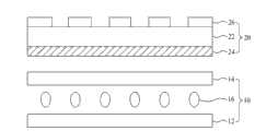
图1是示意性显示现有技术的LCD装置的剖面图。FIG. 1 is a cross-sectional view schematically showing a related art LCD device.
如图1中所示,现有技术的LCD装置包括液晶面板10和触摸屏20。As shown in FIG. 1 , a related art LCD device includes a
液晶面板10显示图像,包括下基板12、上基板14以及形成在下基板12与上基板14之间的液晶层16。The
触摸屏20形成在液晶面板10的顶部,感测用户的触摸。触摸屏20包括触摸基板22、形成在触摸基板22底部的第一感测电极24以及形成在触摸基板22顶部的第二感测电极26。The
第一感测电极24在触摸基板22底部横向布置,第二感测电极26在触摸基板22顶部纵向布置。因此,当用户触摸特定位置时,第一和第二感测电极24和26之间的电容在触摸位置处发生变化,因而触摸屏20感测电容发生变化的位置,由此感测用户的触摸位置。The first sensing electrodes 24 are arranged laterally at the bottom of the
然而,因为现有技术的LCD装置具有触摸屏20分离地形成在液晶面板10顶部的结构,所以由于触摸屏20,现有技术的LCD装置的整体厚度增加,制造工艺复杂,且制造成本增加。However, because the related art LCD device has a structure in which the
发明内容Contents of the invention
因此,本发明旨在提供一种基本上克服了由于现有技术的限制和缺点而导致的一个或多个问题的LCD装置及其制造方法。Accordingly, the present invention is directed to providing an LCD device and method of fabricating the same that substantially obviate one or more problems due to limitations and disadvantages of the related art.
本发明的一个方面是提供一种LCD装置及其制造方法,其中用于感测用户触摸的感测电极内置在液晶面板中,因而与现有技术不同,不需要在液晶面板顶部分离地设置触摸屏,由此减小了LCD装置的厚度,简化了制造工艺,并节省了制造成本。An aspect of the present invention is to provide an LCD device and a method of manufacturing the same, in which a sensing electrode for sensing a user's touch is built into a liquid crystal panel, thereby eliminating the need to separately provide a touch panel on top of a liquid crystal panel unlike the prior art , thereby reducing the thickness of the LCD device, simplifying the manufacturing process, and saving the manufacturing cost.
在下面的描述中将列出本发明的其它优点和特点,这些优点和特点的一部分对于所属领域普通技术人员来说在研究下文之后将是显而易见的,或者可通过本发明的实施领会到。通过说明书、权利要求书以及附图中具体指出的结构可实现和获得本发明的这些目的和其他优点。Other advantages and features of the present invention will be listed in the following description, and part of these advantages and features will be obvious to those of ordinary skill in the art after studying the following, or can be understood through the practice of the present invention. The objectives and other advantages of the invention will be realized and attained by the structure particularly pointed out in the written description and claims hereof as well as the appended drawings.
为了实现这些和其他优点,根据本发明的用途,如在此具体化和概括描述的,提供了一种液晶显示(LCD)装置,包括:在下基板上交叉布置以限定多个像素的多条栅极线和多条数据线;形成在每个像素中的像素电极;通过图案化形成的多个公共电极块,所述多个公共电极块用于与所述像素电极一起产生电场并感测用户的触摸;多条感测线,其中当所述感测线与所述多个公共电极块之一电连接时,所述感测线与其他公共电极块电绝缘;多个焊盘部,所述多个焊盘部被形成为沿相应感测线以预定间隔彼此分离,且所述多个焊盘部具有比所述感测线宽的线宽度;和接触部,所述接触部形成在相应焊盘部与相应公共电极块之间,且所述接触部将相应感测线与公共电极块电连接,其中所述接触部被形成为与电连接到所述多个公共电极块之一的相应感测线中包含的多个焊盘部中的至少一个或多个接触。To achieve these and other advantages, in accordance with the uses of the present invention, as embodied and broadly described herein, there is provided a liquid crystal display (LCD) device comprising: a plurality of grids arranged across a lower substrate to define a plurality of pixels a pole line and a plurality of data lines; a pixel electrode formed in each pixel; a plurality of common electrode blocks formed by patterning for generating an electric field together with the pixel electrodes and sensing a user touch; a plurality of sensing lines, wherein when the sensing line is electrically connected to one of the plurality of common electrode blocks, the sensing line is electrically insulated from other common electrode blocks; a plurality of pad parts, the The plurality of pad portions are formed to be separated from each other at predetermined intervals along the corresponding sensing lines, and the plurality of pad portions have a line width wider than the sensing line; and a contact portion formed on Between the corresponding pad portion and the corresponding common electrode block, and the contact portion electrically connects the corresponding sensing line to the common electrode block, wherein the contact portion is formed to be electrically connected to one of the plurality of common electrode blocks At least one or more contacts of the plurality of pad portions included in the corresponding sensing line.
在本发明的另一个方面中,提供了一种制造LCD装置的方法,包括:在下基板上依次形成栅极、栅极介电层、半导体层、源极、漏极和第一保护层;以及形成与所述漏极电连接的像素电极、通过图案化形成的多个公共电极块、多条感测线、多个焊盘部以及接触部,其中所述多个公共电极块用于与所述像素电极一起产生电场并感测用户的触摸,所述多个焊盘部被形成为沿相应感测线以预定间隔彼此分离且具有比所述感测线宽的线宽度,所述接触部形成在相应焊盘部与相应公共电极块之间,且所述接触部将相应感测线与公共电极块电连接,其中当所述感测线与所述多个公共电极块之一电连接时,所述感测线与其他公共电极块电绝缘,其中所述接触部被形成为与多个焊盘部中的至少一个或多个接触,多个焊盘部中的所述至少一个或多个形成在电连接的相应公共电极块和相应感测线重叠的区域中。In another aspect of the present invention, there is provided a method of manufacturing an LCD device, comprising: sequentially forming a gate, a gate dielectric layer, a semiconductor layer, a source, a drain, and a first protective layer on a lower substrate; and forming a pixel electrode electrically connected to the drain, a plurality of common electrode blocks formed by patterning, a plurality of sensing lines, a plurality of pad portions, and a contact portion, wherein the plurality of common electrode blocks are used to communicate with the The pixel electrodes together generate an electric field and sense a user's touch, the plurality of pad parts are formed to be separated from each other at predetermined intervals along the corresponding sensing lines and have a line width wider than the sensing lines, and the contact parts formed between the corresponding pad portion and the corresponding common electrode block, and the contact portion electrically connects the corresponding sensing line to the common electrode block, wherein when the sensing line is electrically connected to one of the plurality of common electrode blocks , the sensing line is electrically insulated from other common electrode blocks, wherein the contact portion is formed to be in contact with at least one or more of the plurality of pad portions, and the at least one or more of the plurality of pad portions A plurality is formed in a region where the electrically connected corresponding common electrode blocks and corresponding sensing lines overlap.
应当理解,本发明前面的大致描述和下面的详细描述都是例示性的和解释性的,意在对要求保护的本发明提供进一步的解释。It is to be understood that both the foregoing general description and the following detailed description of the present invention are exemplary and explanatory and are intended to provide further explanation of the invention as claimed.
附图说明Description of drawings
给本发明提供进一步理解并且并入到本申请中组成本申请一部分的附图图解了本发明的实施方式,并与说明书一起用于解释本发明的原理。在附图中:The accompanying drawings, which are included to provide a further understanding of the invention and are incorporated in and constitute a part of this application, illustrate embodiments of the invention and together with the description serve to explain the principle of the invention. In the attached picture:
图1是示意性显示现有技术的LCD装置的剖面图;1 is a cross-sectional view schematically showing a prior art LCD device;
图2是示意性显示根据本发明的LCD装置的平面图;2 is a plan view schematically showing an LCD device according to the present invention;
图3是用于描述在根据本发明的LCD装置的感测线中感测用户触摸位置的原理的示图;3 is a diagram for describing the principle of sensing a user's touch position in a sensing line of an LCD device according to the present invention;
图4是显示根据本发明的LCD装置的一个实施方式的示图;FIG. 4 is a diagram showing an embodiment of an LCD device according to the present invention;
图5是显示与沿图4的线A-A所取的剖面对应的第一个实施方式的示图;Fig. 5 is a diagram showing a first embodiment corresponding to a section taken along line A-A of Fig. 4;
图6是显示与沿图4的线B-B所取的剖面对应的第一个实施方式的示图;FIG. 6 is a diagram showing a first embodiment corresponding to a section taken along line B-B of FIG. 4;
图7是显示与沿图4的线A-A所取的剖面对应的第二个实施方式的示图;FIG. 7 is a diagram showing a second embodiment corresponding to a section taken along line A-A of FIG. 4;
图8是显示与沿图4的线B-B所取的剖面对应的第二个实施方式的示图;FIG. 8 is a diagram showing a second embodiment corresponding to a section taken along line B-B of FIG. 4;
图9是显示与沿图4的线A-A所取的剖面对应的第三个实施方式的示图;FIG. 9 is a diagram showing a third embodiment corresponding to a section taken along line A-A of FIG. 4;
图10是显示与沿图4的线B-B所取的剖面对应的第三个实施方式的示图;FIG. 10 is a diagram showing a third embodiment corresponding to a section taken along line B-B of FIG. 4;
图11A到11C是显示根据本发明一个实施方式的制造LCD装置的方法的剖面图;以及11A to 11C are cross-sectional views showing a method of manufacturing an LCD device according to an embodiment of the present invention; and
图12A到12D是显示根据本发明另一实施方式的制造LCD装置的方法的剖面图。12A to 12D are cross-sectional views showing a method of manufacturing an LCD device according to another embodiment of the present invention.
具体实施方式Detailed ways
现在详细描述本发明的典型实施方式,附图中图解了这些实施方式的一些例子。尽可能地在整个附图中将使用相同的参考数字表示相同或相似的部件。Reference will now be made in detail to exemplary embodiments of the present invention, some examples of which are illustrated in the accompanying drawings. Wherever possible, the same reference numbers will be used throughout the drawings to refer to the same or like parts.
下文将参照附图详细描述根据本发明的LCD装置及其制造方法。Hereinafter, an LCD device and a method of manufacturing the same according to the present invention will be described in detail with reference to the accompanying drawings.
在对本发明实施方式的描述中,当描述一结构形成在另一结构上部/下部或者形成在其他结构上/下时,则该描述应当理解为包括上述结构彼此接触的情形,也包括在其间设置第三结构的情形。In the description of the embodiments of the present invention, when it is described that a structure is formed on/under another structure or on/under another structure, the description should be understood to include the situation where the above structures are in contact with each other, and also includes The case of the third structure.
<LCD装置><LCD device>
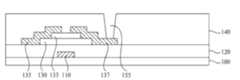
图2是示意性显示根据本发明的LCD装置的平面图。图3是用于描述在根据本发明的LCD装置的感测线中感测用户触摸位置的原理的示图。图4是显示根据本发明的LCD装置的一个实施方式的示图。FIG. 2 is a plan view schematically showing an LCD device according to the present invention. FIG. 3 is a diagram for describing the principle of sensing a user's touch position in a sensing line of an LCD device according to the present invention. FIG. 4 is a diagram showing an embodiment of an LCD device according to the present invention.
如图2到4中所示,根据本发明的LCD装置包括下基板100、栅极线102、数据线104、栅极110、半导体层130、源极135、漏极137、像素电极150、感测线160、焊盘部163、接触部165、公共电极块180、狭缝190、上基板200、多路复用器300和感测电路部400。As shown in FIGS. 2 to 4, the LCD device according to the present invention includes a
下基板100可由玻璃或透明塑料形成。The
栅极线102在下基板100上横向(或沿宽度方向)布置,数据线104在下基板100上纵向(或沿长度方向)布置。多条栅极线102和多条数据线104交叉布置,以限定多个像素。The
栅极线102被示出以直线形状布置,数据线104被示出以直线形状布置。然而,本发明并不限于此。作为另一个例子,数据线104可以以曲线形状布置。The
在每个像素中形成作为开关元件的薄膜晶体管(TFT)。TFT包括栅极110、半导体层130、源极135和漏极137。TFT可以以栅极110设置在半导体层130下方的底栅结构形成,或者以栅极110设置在半导体层130上方的顶栅结构形成。A thin film transistor (TFT) as a switching element is formed in each pixel. The TFT includes a
在每个像素中形成像素电极150,具体地,以对应于每个像素类型的方式形成像素电极150。The
感测线160包括焊盘部163,并向公共电极块180施加电信号。感测线160与公共电极块180电连接,感测电路部400与感测线160的末端连接。因而,当用户触摸公共电极块180时,电信号通过感测线160施加给感测电路部400,因而感测用户的触摸位置。The
当感测线160与多个公共电极块180中的一个电连接时,感测线60与其他的公共电极块180电绝缘,以检测用户的触摸位置。When the
将参照图3进行详细描述。在图3中,显示了四个公共电极块A到D(180)和四条感测线L1到L4(160)。A detailed description will be made with reference to FIG. 3 . In FIG. 3 , four common electrode blocks A to D ( 180 ) and four sensing lines L1 to L4 ( 160 ) are shown.
如图3中所示,感测线L1(160)通过接触部165与公共电极块A(180)连接,并与其他公共电极块B到D(180)电绝缘。因而,当用户触摸公共电极块A(180)时,对应于触摸的电信号传输到感测线L1(160),因而检测用户的触摸位置。As shown in FIG. 3 , the sensing line L1 ( 160 ) is connected with the common electrode block A ( 180 ) through the
以这种方式,感测线L2(160)通过接触部165与公共电极块B(180)连接,并与其他公共电极块A,C和D(180)电绝缘。因而,当用户触摸公共电极块B(180)时,对应于触摸的电信号传输到感测线L2(160),因而检测用户的触摸位置。In this way, the sensing line L2 ( 160 ) is connected with the common electrode block B ( 180 ) through the
感测线L3(160)通过接触部165与公共电极块C(180)连接,并与其他公共电极块A,B和D(180)电绝缘。因而,当用户触摸公共电极块C(180)时,对应于触摸的电信号传输到感测线L3(160),因而检测用户的触摸位置。The sensing line L3 ( 160 ) is connected to the common electrode block C ( 180 ) through the
感测线L4(160)通过接触部165与公共电极块D(180)连接,并与其他公共电极块A到C(180)电绝缘。因而,当用户触摸公共电极块D(180)时,对应于触摸的电信号传输到感测线L4(160),因而检测用户的触摸位置。The sensing line L4 ( 160 ) is connected with the common electrode block D ( 180 ) through the
根据公共电极块180和感测线160的上述结构,仅通过使用被形成为仅在下基板100的一个方向上延伸的感测线160,就可在X-Y平面上检测用户的触摸位置。According to the above structure of the
因此,与在两个方向(即X轴方向和Y轴方向)上形成感测线160的现有技术的LCD装置相比,本发明可简化LCD装置的结构并节省成本。Therefore, the present invention can simplify the structure of the LCD device and save costs compared to the related art LCD device in which the
感测线160向公共电极块180施加电信号,并减小公共电极的电阻。The
公共电极块180一般由诸如氧化铟锡(ITO)这样的透明材料形成,但透明材料具有高电阻。为此,通过将感测线160(由具有出色导电性的金属材料形成)与公共电极块180连接,可降低公共电极块180的电阻。例如,感测线160可由选自Mo、Al、Cu及其合金中的一种材料形成。The
感测线160可形成在平行于栅极线102的方向或者平行于数据线104的方向上。根据本发明,尽管感测线160可形成在平行于栅极线102的方向或者平行于数据线104的方向上,但在X-Y坐标平面上检测用户的触摸位置。The
然而,由于感测线160,开口率减小。为可克服此缺陷,平行于数据线104形成的感测线160可与数据线104重叠,此外,平行于栅极线102形成的感测线160可与栅极线102重叠。However, due to the
焊盘部163被形成为多个,多个焊盘部163沿感测线160以预定间隔彼此分离。焊盘部163可被形成为具有比感测线160宽的线宽度。也就是说,感测线160通过接触焊盘部163的接触部165与公共电极块180电连接。为了实现感测线160与公共电极块180之间的平稳连接,感测线160可包括具有比感测线160宽的线宽度的焊盘部163。The
在这种情形中,不考虑焊盘部163是否与接触部165连接,焊盘部163都可被形成为具有恒定的线宽度。也就是说,为了感测线160与公共电极块180之间的连接,在感测线160上形成焊盘部163,但不考虑在焊盘部163上方(或下方)是否具有接触部165,焊盘部163都被形成为具有恒定的线宽度。In this case, regardless of whether the
作为一个例子进行描述,如图3中所示,在与公共电极块A(180)重叠的区域中,沿感测线L1(160)以确定间隔形成四个焊盘部163,尽管仅在四个焊盘部163之一中形成接触部165,但四个焊盘部163被形成为具有相同的线宽度。Described as an example, as shown in FIG. 3 , in the region overlapping with the common electrode block A ( 180 ), four
焊盘部163被形成为多个,多个焊盘部163沿感测线160以确定间隔彼此分离。如图3中所示,在一个实施方式中,焊盘部163可以以确定间隔彼此分离,在每个像素中可形成一个焊盘部163。此外,如图4中所示,焊盘部163可正好形成在栅极线102下方。在上述实施方式中,描述了在每个像素中形成一个焊盘部163且该一个焊盘部163正好形成在栅极线102下方,但根据本发明的LCD装置的焊盘部163并不限于此。The
一条感测线160包括被形成为以确定间隔彼此分离的多个焊盘部163,焊盘部163形成在与相邻感测线160中包含的焊盘部163对称的各个位置处。One
在一个实施方式中,如图3中所示,感测线L1(160)中包含的多个焊盘部163形成在与相邻的感测线L2(160)中包含的多个焊盘部163对称的各个位置处。也就是说,感测线L1(160)的第一焊盘部163和感测线L2(160)的第一焊盘部163在与感测线160的长度方向垂直的方向上形成在一条直线上。In one embodiment, as shown in FIG. 3 , the plurality of
当仅在与形成有接触部165的位置对应的感测线160中形成焊盘部163,或者焊盘部163不是形成在与相邻感测线160的焊盘部163对称的位置时,在再现图像时由于感测线160的非均匀的线宽度,在显示面板的表面中出现斑点。所述斑点是由于设置在像素电极150附近的焊盘部163产生的寄生电容的非均匀分布导致的,在这种情形中,寄生电容的分布形式可以是各种形式,如旗帜形式(flag form)。When the
然而,当沿感测线160以确定间隔彼此分离地形成的多个焊盘部163形成在与相邻感测线160的焊盘部163对称的各个位置处时,寄生电容均匀分布在显示面板的整个表面上,因而当再现图像时可防止显示面板的表面的斑点。However, when a plurality of
接触部165形成在焊盘部163与公共电极块180之间,并与感测线160和公共电极块180电连接。The
感测线160包括以确定间隔彼此分离地形成的多个焊盘部163,在这种情形中,接触部165形成在多个焊盘部163中的至少一个或多个上方(或下方),并与感测线160和公共电极块180电连接。The
在这种情形中,如上所述,当一条感测线160与一个公共电极块180电连接时,这一条感测线160与其他公共电极块180电绝缘,因而,相对于这一条感测线160来说,接触部165不会同时形成在不同的公共电极块180中。In this case, as described above, when one
作为一个例子结合图3进行描述,当感测线L1(160)通过接触部165与公共电极块A(180)电连接时,在感测线L1与其他公共电极块B到D(180)重叠的区域中不形成接触部165。As an example described in conjunction with FIG. 3 , when the sensing line L1 ( 160 ) is electrically connected to the common electrode block A ( 180 ) through the
接触部165可被形成为与电连接到多个公共电极块180之一的感测线160中包含的多个焊盘部163中的至少一个或多个接触。或者,接触部165被形成为与多个焊盘部中的至少一个或多个接触,所述至少一个或多个形成在电连接的相应公共电极块和相应感测线重叠的区域中。The
作为一个例子参照图3进行描述。在图3中,感测线L1(160)被示出通过一个接触部165与公共电极块A(180)电连接。然而,因为在公共电极块A(180)与感测线L1(160)重叠的区域中总共形成四个焊盘部163,所以接触部165可被形成为与四个焊盘部163中的至少一个或多个接触。Description will be made with reference to FIG. 3 as an example. In FIG. 3 , the sensing line L1 ( 160 ) is shown to be electrically connected to the common electrode block A ( 180 ) through one
为防止开口率减小,接触部165可形成在非透射区域中。非透射区域是除了其中光穿过像素的区域之外的其他区域,例如非透射区域表示其中形成数据线104和栅极线102的区域。To prevent the reduction of the aperture ratio, the
在图4中,接触部165被示出与栅极线102相邻地形成,但并不限于此。根据情况,接触部165可与数据线104和源极135相邻地形成。In FIG. 4 , the
公共电极块180形成在与像素电极150不同的层上,公共电极块180和像素电极150一起产生驱动液晶的电场。也就是说,公共电极块180用作感测用户触摸位置的感测电极。The
为了利用公共电极块180作为感测电极,公共电极块180被形成为多个,在这种情形中,多个公共电极块180以确定图案彼此分离。公共电极块180可被形成为具有与一个或多个像素对应的尺寸,具体地,公共电极块180的尺寸与多少个像素对应是依赖于LCD装置的触摸分辨率。In order to use the
也就是说,当与一定数量的像素对应的区域被形成为一个公共电极块180时,触摸分辨率与像素的数量成反比地下降。例如,当与太少数量的像素对应的区域被形成为一个公共电极块180时,触摸分辨率增加,但感测线160的数量也增加。That is, when an area corresponding to a certain number of pixels is formed as one
在像素电极150或公共电极块180内,可形成至少一个或多个狭缝190。In the
这样,当在像素电极150或公共电极块180内设置狭缝190时,可通过狭缝190在像素电极150与公共电极块180之间产生边缘场,并可由边缘场驱动液晶。也就是说,可由边缘场切换模式实现LCD装置。In this way, when the
当在公共电极块180内设置狭缝190时,多个公共电极块180形成在像素电极150上,且在多个公共电极块180与像素电极150之间具有第二保护层170(见图7)。When the
另一方面,当在像素电极150内设置狭缝190时,像素电极150形成在公共电极块180上,且在像素电极150与公共电极块180之间具有第二保护层170(见图5)。On the other hand, when the
上基板200与下基板100相面对地结合,并在上基板200与下基板100之间形成液晶层。The
尽管未示出,但在上基板200的后表面可形成高电阻导电层(未示出)。高电阻导电层是透过从液晶面板入射的光的透明材料,且高电阻导电层由下述导电材料形成,所述导电材料具有用于将电荷(由液晶面板上的静电产生)接地到形成在下基板100中的接地焊盘(未示出)的导电率。高电阻导电层被形成为具有高电阻率(例如50MΩ/sqr(方块)到5GΩ/sqr),用于提高检测用户触摸的性能。Although not shown, a high resistance conductive layer (not shown) may be formed on the rear surface of the
高电阻导电层使液晶面板中产生的电荷流到接地端(GND),由此提高了内置有触摸电极的LCD装置的静电放电(ESD)屏蔽性能。The high-resistance conductive layer allows charges generated in the liquid crystal panel to flow to the ground (GND), thereby improving electrostatic discharge (ESD) shielding performance of LCD devices with built-in touch electrodes.
也就是说,如上所述,高电阻导电层由具有50MΩ/sqr到5GΩ/sqr电阻率值的高电阻材料形成,防止对用户手指作用的屏蔽,因而提高了内置有触摸屏的LCD装置的触摸检测性能。That is, as described above, the high-resistance conductive layer is formed of a high-resistance material having a resistivity value of 50MΩ/sqr to 5GΩ/sqr, preventing shielding of the user's finger, thereby improving touch detection of an LCD device with a built-in touch screen. performance.
多路复用器(MUX)300连接在感测线160与感测电路部400之间,且优选地连接每条感测线的末端,其减少感测电路部400中设置的感测线160的数量。A multiplexer (MUX) 300 is connected between the
在图2中,作为一个例子显示了4:1多路复用器300,但并不限于此。可使用具有各种组合的多路复用器300,如8:1多路复用器或16:1多路复用器。In FIG. 2, a 4:1
当使用多路复用器300时,减少了感测电路部400中设置的感测线160的数量,因而减小了边框宽度,提高了外部的开口率。When the
多路复用器300可形成在形成有感测线160的下基板100上、内置在驱动IC中、或者由单独的多路复用器300芯片实现。The
感测电路部400与感测线160直接连接或者通过多路复用器300与感测线160连接,并且当用户触摸公共电极块180时,感测电路部400使用沿感测线160施加的信号来感测是否存在触摸以及触摸位置。The
下文将参照图5到10更详细地描述本发明的各个实施方式,图5到10显示了根据本发明的LCD装置的剖面结构。Various embodiments of the present invention will be described in more detail below with reference to FIGS. 5 to 10 showing a cross-sectional structure of an LCD device according to the present invention.
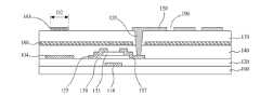
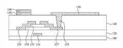
图5是显示与沿图4的线A-A所取的剖面对应的第一个实施方式的示图。图6是显示与沿图4的线B-B所取的剖面对应的第一个实施方式的示图。FIG. 5 is a view showing the first embodiment corresponding to a section taken along line A-A of FIG. 4 . FIG. 6 is a view showing the first embodiment corresponding to a section taken along line B-B of FIG. 4 .
如图5和6中所示,根据本发明第一个实施方式的LCD装置包括下基板100、栅极110、栅极介电层120、半导体层130、蚀刻阻止层133、源极135、漏极137、第一保护层140、像素电极150、感测线160(见图4)、焊盘部163、接触部165、第二保护层170和公共电极块180。LCD装置具有像素电极150形成在公共电极块180上的顶部像素电极结构。As shown in FIGS. 5 and 6, the LCD device according to the first embodiment of the present invention includes a
下基板100可由玻璃或透明塑料形成。The
栅极110从形成在下基板100上的栅极线102分支并由导电材料形成。The
在栅极110上形成栅极介电层120,栅极介电层120可由SiOX或SiNX形成。A
在栅极介电层120上与栅极110相对应的位置处形成半导体层130。当向栅极110施加栅极电压时,形成使电流能够在源极135与漏极137之间流动的沟道。半导体层130可以是氧化物或非晶半导体。The
在半导体层130上形成蚀刻阻止层133,蚀刻阻止层133保护半导体层130。蚀刻阻止层133可由SiOX或SiNX形成。然而,根据情况,可不设置蚀刻阻止层133。An
源极135被形成为从数据线104延伸并由低电阻导体形成,以使由于面板负载导致的TFT的操作延迟最小化。The
在半导体层130上与源极135隔开地形成漏极137。漏极137由导体形成,其可以是透明导体,如ITO。The
在源极135和漏极137上形成第一保护层140,第一保护层140可由SiOX或SiNX形成。A first
在第一保护层140上形成公共电极块180。这里,可以以确定间隔形成多个公共电极块180,用于防止像素电极150和公共电极块180以后在像素电极接触孔155的位置中电短路。A
在公共电极块180上形成第二保护层170,第二保护层170可由SiOX或SiNX形成。A second
在第二保护层170上形成感测线160(见图4)、焊盘部163和接触部165。感测线160(见图4)中包含的焊盘部163和公共电极块180通过接触部165电连接。The sensing line 160 (see FIG. 4 ), the
在这种情形中,在显示沿图4的线A-A所取的剖面图的图5中,接触部165形成在焊盘部163下方。然而,在显示沿图4的线B-B所取的剖面图的图6中,可不设置接触部165。如上所述,这是因为当一条感测线与一个公共电极块180电连接时,这条感测线与其他公共电极块180绝缘,因而不是在所有焊盘部163下方都形成接触部165。In this case, in FIG. 5 showing a cross-sectional view taken along line A-A of FIG. 4 , the
不考虑是否形成接触部165,焊盘部163的线宽度D1和D2都相等。如上所述,这是因为当沿感测线形成的焊盘部163不是设置在对称位置或者焊盘部163的线宽度不同时,在显示面板上会形成斑点。Regardless of whether the
在第二保护层170上,与焊盘部163隔开地形成像素电极150。像素电极150通过像素电极接触孔155与漏极137电连接。On the
在这种情形中,在像素电极150内设置狭缝190。通过狭缝190可在像素电极150与公共电极块180之间产生边缘场,由边缘场驱动液晶。也就是说,可由边缘场切换模式实现LCD装置。In this case, the
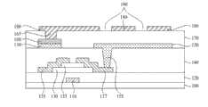
图7是显示与沿图4的线A-A所取的剖面对应的第二个实施方式的示图。图8是显示与沿图4的线B-B所取的剖面对应的第二个实施方式的示图。FIG. 7 is a diagram showing a second embodiment corresponding to a section taken along line A-A of FIG. 4 . FIG. 8 is a diagram showing a second embodiment corresponding to a section taken along line B-B of FIG. 4 .
如图7和8中所示,根据本发明第二个实施方式的LCD装置包括下基板100、栅极110、栅极介电层120、半导体层130、蚀刻阻止层133、源极135、漏极137、第一保护层140、像素电极150、感测线160(见图4)、焊盘部163、接触部165、第二保护层170和公共电极块180。LCD装置具有公共电极块180形成在像素电极150上的顶部公共电极块结构。除了顶部公共电极块结构之外,图7和8的实施方式与图5和6的实施方式相同,因而不再进行重复描述。As shown in FIGS. 7 and 8, an LCD device according to a second embodiment of the present invention includes a
在第一保护层140上形成像素电极150,像素电极150可由诸如ITO这样的透明导体形成。像素电极150通过形成在第一保护层140上的像素电极接触孔155与漏极137电连接。A
在与像素电极150相同的层上,与像素电极150隔开地形成焊盘部163。焊盘部163可由选自Mo、Al、Cu及其合金中的一种材料形成。On the same layer as the
在像素电极150和焊盘部163上形成第二保护层170,第二保护层170可由SiOX或SiNX形成。The second
在第二保护层170上形成公共电极块180,公共电极块180可由诸如ITO这样的透明导体形成。公共电极块180通过接触部165与焊盘部163电连接。A
在这种情形中,可以看到图7中在焊盘部163上形成有接触部165,但在图8中没有设置接触部165。如上所述,当一条感测线与一个公共电极块180电连接时,这条感测线与其他公共电极块180绝缘,因而不是在所有焊盘部163上都形成接触部165。In this case, it can be seen that the
不考虑是否形成接触部165,焊盘部163的线宽度D1和D2都相等。如上所述,这是因为当沿感测线形成的焊盘部163不是设置在对称位置或者焊盘部163的线宽度不同时,在显示面板上会形成斑点。Regardless of whether the
在这种情形中,在公共电极块180内设置狭缝190。可通过狭缝190在像素电极150与公共电极块180之间产生边缘场,由边缘场驱动液晶。也就是说,可由边缘场切换模式实现LCD装置。In this case, a
图9是显示与沿图4的线A-A所取的剖面对应的第三个实施方式的示图。图10是显示与沿图4的线B-B所取的剖面对应的第三个实施方式的示图。FIG. 9 is a diagram showing a third embodiment corresponding to a section taken along line A-A of FIG. 4 . FIG. 10 is a diagram showing a third embodiment corresponding to a section taken along line B-B of FIG. 4 .
如图9和10中所示,根据本发明第三个实施方式的LCD装置包括下基板100、栅极110、栅极介电层120、半导体层130、蚀刻阻止层133、源极135、漏极137、第一保护层140、像素电极150、感测线160(见图4)、焊盘部163、接触部165、第二保护层170和公共电极块180。LCD装置具有公共电极块180形成在像素电极150上的顶部公共电极块结构。除了像素电极150和焊盘部163的垂直结构之外,图9和10的实施方式与图7和8的实施方式相同,因而不再进行重复描述。As shown in FIGS. 9 and 10, an LCD device according to a third embodiment of the present invention includes a
在焊盘部163下方形成像素电极150。也就是说,焊盘部163形成在像素电极150上,但与焊盘部163重叠的像素电极150与电连接到漏极137的像素电极150电绝缘。The
可以按如下方式实现这种结构。通过光刻工艺形成像素电极150,然后通过分离的光刻工艺形成感测线160(见图4)和焊盘部163,由此实现所述结构。然而,可使用半色调掩模工艺有效实现所述结构。This structure can be implemented as follows. The structure is realized by forming the
也就是说,当通过使用半色调掩模工艺在一道光刻工艺中同时形成像素电极150和感测线160时,本发明可将用于形成像素电极150和感测线160的两道掩模工艺简化为一道掩模工艺。That is, when the
因此,代替两次曝光工艺,通过进行一次曝光工艺,可缩短粘性时间(tacktime),节省了曝光工艺中使用的材料成本。Therefore, by performing one exposure process instead of two exposure processes, tack time can be shortened, saving material costs used in the exposure process.
<制造LCD装置的方法><Method of Manufacturing LCD Device>
图11A到11C是显示根据本发明一个实施方式的制造LCD装置的方法的剖面图。11A to 11C are cross-sectional views showing a method of manufacturing an LCD device according to an embodiment of the present invention.
首先,如图11A中所示,在下基板100上依次形成栅极110、栅极介电层120、半导体层130、蚀刻阻止层133、源极135、漏极137和第一保护层140。尽管未示出,但在下基板100中形成栅极线101和数据线104。First, as shown in FIG. 11A , a
随后,如图11B中所示,在第一保护层140上形成像素电极接触孔155,然后通过形成像素电极150,漏极137与像素电极150电连接。此外,在确定位置处形成感测线160。Subsequently, as shown in FIG. 11B , a pixel
可在平行于栅极线102的方向或平行于数据线104的方向上形成感测线160。根据本发明,尽管可在平行于栅极线102的方向或平行于数据线104的方向上形成感测线160,但在X-Y坐标平面上检测用户的触摸位置。The
在这种情形中,由于感测线160,开口率减小。为了克服此缺陷,平行于数据线104形成的感测线160可与数据线104重叠,此外,平行于栅极线102形成的感测线160可与栅极线102重叠。In this case, the aperture ratio decreases due to the
多条感测线160以确定间隔彼此分离,每条感测线160都包括多个焊盘部163(见图3),焊盘部具有比感测线160宽的线宽度。The plurality of
随后,如图11C中所示,在像素电极150和感测线160上形成第二保护层170,然后通过形成接触部165,感测线160与公共电极块180电连接。Subsequently, as shown in FIG. 11C , the second
在这种情形中,当感测线160与多个公共电极块180之一电连接时,感测线160与其他公共电极块180电绝缘,因而接触部165形成在一条感测线160与一个公共电极块电连接的位置处。In this case, when the
通过在第二保护层170上形成公共电极块180,感测线160与公共电极块180电连接。The
因为公共电极块180用作感测电极,所以公共电极块180被形成为多个,以具有确定图案。公共电极块180可被形成为具有与一个或多个像素对应的尺寸,公共电极块180的尺寸与多少个像素对应是依赖于LCD装置的触摸分辨率。Since the
<制造利用半色调掩模形成的LCD装置的方法><Method of Manufacturing LCD Device Formed Using Halftone Mask>
图12A到12D是显示根据本发明另一实施方式的制造LCD装置的方法的剖面图。下面的描述集中在不与图11A至11C重复的构造上。12A to 12D are cross-sectional views showing a method of manufacturing an LCD device according to another embodiment of the present invention. The following description focuses on configurations that do not overlap with FIGS. 11A to 11C .
首先,如图12A中所示,在下基板100上依次形成栅极110、栅极介电层120、半导体层130、蚀刻阻止层133、源极135、漏极137和第一保护层140。在第一保护层140上形成像素电极接触孔155。First, as shown in FIG. 12A , a
随后,如图12B中所示,在第一保护层140上依次叠置像素电极层150a和感测线层140a。Subsequently, as shown in FIG. 12B , the
在像素电极层150a和感测线层140a上叠置光刻胶,并使用半色调掩模700照射光。这里,半色调掩模700包括不能透射光的非透射区域710、仅透过部分光的半透射区域720、以及透射全部光的透射区域730a到730c。A photoresist is stacked on the
随后,通过将光刻胶显影,形成光刻胶图案。在光刻胶图案中,与半色调掩模700的非透射区域710对应的光刻胶层被原样留下,与半色调掩模700的半透射区域720对应的光刻胶层被部分留下,与半色调掩模700的透射区域730a到730c对应的光刻胶层全部被移除。Subsequently, by developing the photoresist, a photoresist pattern is formed. In the photoresist pattern, the photoresist layer corresponding to the
随后,如图12C中所示,使用光刻胶图案作为掩模来蚀刻像素电极层150a和感测线层140a。对光刻胶图案进行灰化工艺,然后对光刻胶图案进行蚀刻工艺,由此最终移除光刻胶图案。Subsequently, as shown in FIG. 12C, the
当以如此方式形成像素电极150和感测线160时,照射光的工艺不是进行两次,而是进行一次,因而节省了制造时间和成本。When the
随后,如图12D中所示,在像素电极150和感测线160上形成第二保护层170,在第二保护层170上进行图案化以形成公共电极块180。Subsequently, as shown in FIG. 12D , a
根据本发明,用于产生驱动液晶的电场的公共电极(或公共电极块)用作感测用户触摸的感测电极,因而与现有技术不同,不需要在液晶面板顶部分离地设置触摸屏,由此减小了LCD装置的厚度,简化了制造工艺,并节省了制造成本。According to the present invention, the common electrode (or common electrode block) used to generate the electric field for driving the liquid crystal is used as the sensing electrode for sensing the user's touch, so unlike the prior art, there is no need to separately provide a touch screen on top of the liquid crystal panel, by This reduces the thickness of the LCD device, simplifies the manufacturing process, and saves the manufacturing cost.
此外,根据本发明,仅通过使用被形成为仅在下基板的一个方向上延伸的感测线就可在X-Y平面上检测用户的触摸位置,因而与在两个方向(即X轴方向和Y轴方向)上形成感测线的现有技术的LCD装置相比,本发明可简化LCD装置的结构并节省成本。In addition, according to the present invention, the user's touch position can be detected on the X-Y plane only by using the sensing line formed to extend only in one direction of the lower substrate, thus being compatible with the two directions (i.e., the X-axis direction and the Y-axis direction). Compared with the prior art LCD device in which sensing lines are formed in the direction), the present invention can simplify the structure of the LCD device and save cost.
此外,根据本发明,通过使用多路复用器减少了感测电路部内设置的感测线的数量,因而减小了边框宽度,提高了外部的开口率。Furthermore, according to the present invention, the number of sensing lines provided in the sensing circuit portion is reduced by using the multiplexer, thereby reducing the bezel width and increasing the external aperture ratio.
此外,根据本发明,不考虑是否存在接触部,通过形成包括具有恒定线宽度的焊盘部的感测线,可消除显示面板的表面上的斑点。Furthermore, according to the present invention, by forming a sensing line including a pad portion having a constant line width irrespective of the presence or absence of a contact portion, it is possible to eliminate spots on the surface of the display panel.
在不脱离本发明的精神或范围的情况下,在本发明中可进行各种修改和变化,这对于所属领域技术人员来说是显而易见的。因而,本发明意在覆盖落入所附权利要求书范围及其等效范围内的对本发明的所有修改和变化。It will be apparent to those skilled in the art that various modifications and variations can be made in the present invention without departing from the spirit or scope of the inventions. Thus, it is intended that the present invention cover all the modifications and variations of this invention that come within the scope of the appended claims and their equivalents.
Claims (10)
Translated fromChineseApplications Claiming Priority (2)
| Application Number | Priority Date | Filing Date | Title |
|---|---|---|---|
| KR1020120032333AKR101466556B1 (en) | 2012-03-29 | 2012-03-29 | Liquid crystal display device and Method for manufacturing the same |
| KR10-2012-0032333 | 2012-03-29 |
Publications (2)
| Publication Number | Publication Date |
|---|---|
| CN103364983Atrue CN103364983A (en) | 2013-10-23 |
| CN103364983B CN103364983B (en) | 2015-12-09 |
Family
ID=49234263
Family Applications (1)
| Application Number | Title | Priority Date | Filing Date |
|---|---|---|---|
| CN201210524133.XAActiveCN103364983B (en) | 2012-03-29 | 2012-12-07 | Liquid crystal disply device and its preparation method |
Country Status (3)
| Country | Link |
|---|---|
| US (4) | US9098134B2 (en) |
| KR (1) | KR101466556B1 (en) |
| CN (1) | CN103364983B (en) |
Cited By (27)
| Publication number | Priority date | Publication date | Assignee | Title |
|---|---|---|---|---|
| CN104022128A (en)* | 2014-05-30 | 2014-09-03 | 京东方科技集团股份有限公司 | Array substrate, manufacturing method thereof and displaying device |
| CN104020892A (en)* | 2014-05-30 | 2014-09-03 | 京东方科技集团股份有限公司 | In cell touch panel and display device |
| CN104062817A (en)* | 2014-06-23 | 2014-09-24 | 上海天马微电子有限公司 | Liquid crystal display device with touch control function |
| CN104679321A (en)* | 2013-11-28 | 2015-06-03 | 乐金显示有限公司 | Touch Sensor Integrated Type Display Device |
| WO2015089965A1 (en)* | 2013-12-17 | 2015-06-25 | 京东方科技集团股份有限公司 | Display substrate, manufacturing method therefor, touch screen, and display device |
| CN104777637A (en)* | 2015-05-08 | 2015-07-15 | 上海中航光电子有限公司 | Array substrate and touch-control display device and testing method thereof |
| CN105204241A (en)* | 2014-06-20 | 2015-12-30 | 三星显示有限公司 | Liquid crystal display |
| CN105278187A (en)* | 2014-06-24 | 2016-01-27 | 乐金显示有限公司 | Display device integrated with touch screen panel and method for fabricating the same |
| CN105739203A (en)* | 2014-12-31 | 2016-07-06 | 乐金显示有限公司 | In-cell touch liquid crystal display apparatus and method of manufacturing the same |
| CN105739144A (en)* | 2014-12-31 | 2016-07-06 | 乐金显示有限公司 | In-cell touch liquid crystal display device and method of manufacturing the same |
| CN105739193A (en)* | 2014-12-31 | 2016-07-06 | 乐金显示有限公司 | In-cell touch liquid crystal display device and method for manufacturing the same |
| CN105739737A (en)* | 2014-12-26 | 2016-07-06 | 乐金显示有限公司 | Touch sensor integrated type display device |
| WO2016119373A1 (en)* | 2015-01-27 | 2016-08-04 | 京东方科技集团股份有限公司 | Array substrate, touch-control panel and method for manufacturing array substrate |
| CN104022127B (en)* | 2014-05-30 | 2016-10-05 | 京东方科技集团股份有限公司 | A kind of array base palte and preparation method thereof and display device |
| CN104062817B (en)* | 2014-06-23 | 2016-11-30 | 上海天马微电子有限公司 | Liquid crystal display device with touch control function |
| CN106200064A (en)* | 2015-05-29 | 2016-12-07 | 乐金显示有限公司 | In-cell touch liquid crystal display device and manufacture method thereof |
| CN104102402B (en)* | 2014-06-25 | 2017-01-25 | 京东方科技集团股份有限公司 | Touch substrate and display device |
| CN106873226A (en)* | 2017-04-28 | 2017-06-20 | 上海中航光电子有限公司 | A kind of touch-control display panel |
| CN106970493A (en)* | 2017-05-22 | 2017-07-21 | 厦门天马微电子有限公司 | Display panel and display device |
| CN106980421A (en)* | 2015-12-30 | 2017-07-25 | 乐金显示有限公司 | Integrated touch display device |
| CN107065322A (en)* | 2015-11-30 | 2017-08-18 | 乐金显示有限公司 | Touch screen display device and the display device of the integrated touch screen containing it |
| US9766764B2 (en) | 2015-01-30 | 2017-09-19 | Lg Display Co., Ltd. | Touch display apparatus |
| CN107765488A (en)* | 2015-04-01 | 2018-03-06 | 上海天马微电子有限公司 | Array substrate, touch display panel and touch display device |
| CN108110010A (en)* | 2017-12-15 | 2018-06-01 | 京东方科技集团股份有限公司 | Array substrate and preparation method thereof, touch-control display panel |
| CN110376807A (en)* | 2018-04-12 | 2019-10-25 | 夏普株式会社 | Display device |
| CN112750874A (en)* | 2019-10-30 | 2021-05-04 | 三星显示有限公司 | Display device and test method thereof |
| US11710748B2 (en) | 2015-01-27 | 2023-07-25 | Beijing Boe Optoelectronics Technology Co., Ltd. | Array substrate and touch panel and manufacturing method of array substrate |
Families Citing this family (48)
| Publication number | Priority date | Publication date | Assignee | Title |
|---|---|---|---|---|
| KR101466556B1 (en)* | 2012-03-29 | 2014-11-28 | 엘지디스플레이 주식회사 | Liquid crystal display device and Method for manufacturing the same |
| CN103280448B (en)* | 2013-04-27 | 2016-01-06 | 北京京东方光电科技有限公司 | A kind of array base palte and preparation method thereof, display unit |
| KR102104628B1 (en)* | 2013-08-12 | 2020-04-27 | 삼성디스플레이 주식회사 | Touch screen display device |
| JP6165584B2 (en)* | 2013-10-08 | 2017-07-19 | 株式会社ジャパンディスプレイ | Display device |
| KR102159189B1 (en)* | 2013-11-05 | 2020-09-24 | 삼성디스플레이 주식회사 | Display device, touch panel device, touch panel driving ic device and method of driving touch panel |
| CN103699284B (en)* | 2013-12-27 | 2016-09-21 | 京东方科技集团股份有限公司 | A kind of capacitance type in-cell touch panel and preparation method thereof, display device |
| KR102156196B1 (en)* | 2013-12-30 | 2020-09-15 | 엘지디스플레이 주식회사 | Display Panel |
| KR102235495B1 (en)* | 2013-12-31 | 2021-04-02 | 엘지디스플레이 주식회사 | Display Device Integrated With Touch Screen and Method for Driving The Same |
| CN104035640B (en)* | 2014-05-30 | 2017-10-27 | 京东方科技集团股份有限公司 | A kind of In-cell touch panel and display device |
| CN104020893B (en)* | 2014-05-30 | 2017-01-04 | 京东方科技集团股份有限公司 | A kind of In-cell touch panel and display device |
| CN104020907B (en) | 2014-05-30 | 2017-02-15 | 京东方科技集团股份有限公司 | In cell touch panel and display device |
| CN104020910B (en)* | 2014-05-30 | 2017-12-15 | 京东方科技集团股份有限公司 | A kind of In-cell touch panel and display device |
| KR101655410B1 (en)* | 2014-08-26 | 2016-09-07 | 엘지디스플레이 주식회사 | In-cell Touch type liquid crystal display device |
| KR102159560B1 (en)* | 2014-08-29 | 2020-09-25 | 엘지디스플레이 주식회사 | Touch sensor integrated type liquid crystal display device |
| JP6698321B2 (en) | 2014-12-02 | 2020-05-27 | 株式会社半導体エネルギー研究所 | Display device |
| CN104460080A (en)* | 2014-12-04 | 2015-03-25 | 深圳市华星光电技术有限公司 | Touch-control display device |
| CN104484083B (en)* | 2014-12-09 | 2018-07-17 | 深圳市华星光电技术有限公司 | A kind of embedded display screen, terminal and touch detecting method with touch function |
| KR101678590B1 (en)* | 2014-12-26 | 2016-11-23 | 엘지디스플레이 주식회사 | Liquid crystal display panel and liquid crystal display device using the same |
| KR101661039B1 (en)* | 2014-12-30 | 2016-10-11 | 엘지디스플레이 주식회사 | Ultra High Resolution Flat Panel Display Having In-Cell Type Touch Sensor |
| CN104536637A (en)* | 2015-01-29 | 2015-04-22 | 京东方科技集团股份有限公司 | Embedded touch screen and display device |
| CN104571768B (en)* | 2015-01-30 | 2018-03-20 | 京东方科技集团股份有限公司 | A kind of array base palte, In-cell touch panel and display device |
| KR102381121B1 (en)* | 2015-02-02 | 2022-04-01 | 삼성디스플레이 주식회사 | Touch panel and display apparatus having the same |
| US9910530B2 (en)* | 2015-02-27 | 2018-03-06 | Panasonic Liquid Crystal Display Co., Ltd. | Display panel with touch detection function |
| KR102315816B1 (en) | 2015-03-09 | 2021-10-20 | 엘지디스플레이 주식회사 | Liquid crystal display apparatus |
| KR20160114510A (en)* | 2015-03-24 | 2016-10-05 | 가부시키가이샤 한도오따이 에네루기 켄큐쇼 | Touch panel |
| CN104698708B (en)* | 2015-04-01 | 2017-11-10 | 上海天马微电子有限公司 | Array substrate, manufacturing method thereof and display device |
| US9939972B2 (en)* | 2015-04-06 | 2018-04-10 | Synaptics Incorporated | Matrix sensor with via routing |
| CN104777933B (en) | 2015-04-09 | 2018-02-06 | 上海天马微电子有限公司 | Array substrate, touch display panel and display device |
| US10108039B2 (en)* | 2015-05-08 | 2018-10-23 | Xiamen Tianma Micro-Electronics Co., Ltd. | Touch array substrate, liquid crystal display panel and liquid crystal display device |
| CN108919541A (en)* | 2015-05-08 | 2018-11-30 | 厦门天马微电子有限公司 | Touch-control array substrate, liquid crystal display panel and liquid crystal display device |
| CN104915081B (en)* | 2015-06-10 | 2019-03-15 | 京东方科技集团股份有限公司 | Array substrate and preparation method thereof, and touch display panel |
| CN105116583A (en)* | 2015-09-15 | 2015-12-02 | 深圳市华星光电技术有限公司 | Touch structure and liquid crystal display with same |
| CN105117073B (en)* | 2015-09-29 | 2019-02-26 | 京东方科技集团股份有限公司 | A touch display panel and a touch display device |
| CN105259690A (en)* | 2015-10-10 | 2016-01-20 | 武汉华星光电技术有限公司 | Manufacturing method of array substrate, array substrate, and touch control liquid crystal display apparatus |
| KR102427312B1 (en)* | 2015-11-27 | 2022-08-01 | 엘지디스플레이 주식회사 | Organic light-emitting display panel and organic light-emitting display device |
| US10120473B2 (en)* | 2015-12-03 | 2018-11-06 | Lg Display Co., Ltd. | Touch sensor integrated type display device |
| KR102468762B1 (en)* | 2015-12-14 | 2022-11-21 | 엘지디스플레이 주식회사 | Display device with a built-in touch screen and method for driving the same |
| CN105677076B (en)* | 2015-12-28 | 2018-09-25 | 上海天马微电子有限公司 | Touch display device, touch display panel and array substrate |
| CN105630247B (en)* | 2016-02-02 | 2019-01-08 | 上海天马微电子有限公司 | Array substrate |
| CN106125390A (en)* | 2016-08-19 | 2016-11-16 | 武汉华星光电技术有限公司 | Display panels and liquid crystal indicator |
| CN106098710A (en)* | 2016-08-29 | 2016-11-09 | 京东方科技集团股份有限公司 | A kind of array base palte and preparation method thereof, display device |
| KR102369337B1 (en)* | 2017-07-11 | 2022-03-04 | 삼성디스플레이 주식회사 | Input sensing unit and display device having the same |
| CN107463292B (en)* | 2017-08-04 | 2020-08-21 | 武汉天马微电子有限公司 | Display panel, display device and driving method of display panel |
| KR102463812B1 (en)* | 2018-04-03 | 2022-11-03 | 엘지디스플레이 주식회사 | Touch display device and touch sensing method |
| KR102569929B1 (en)* | 2018-07-02 | 2023-08-24 | 삼성디스플레이 주식회사 | Display apparatus |
| US11086461B2 (en)* | 2019-01-02 | 2021-08-10 | Boe Technology Group Co., Ltd. | Array substrate, embedded touch screen, and display device |
| JP2022054101A (en)* | 2020-09-25 | 2022-04-06 | シャープ株式会社 | Liquid crystal display device |
| JP2023109565A (en) | 2022-01-27 | 2023-08-08 | 株式会社ジャパンディスプレイ | Display device with touch detection function |
Citations (5)
| Publication number | Priority date | Publication date | Assignee | Title |
|---|---|---|---|---|
| KR20070082757A (en)* | 2006-02-17 | 2007-08-22 | 삼성전자주식회사 | Touch screen display |
| CN101681221A (en)* | 2008-03-28 | 2010-03-24 | 索尼株式会社 | Display device provided with touch sensor |
| CN102109722A (en)* | 2009-12-28 | 2011-06-29 | 乐金显示有限公司 | Liquid crystal display device and method of fabricating same |
| KR20110100377A (en)* | 2010-03-04 | 2011-09-14 | 엘지디스플레이 주식회사 | Liquid crystal display panel with a built-in touch screen and liquid crystal display device including the same |
| KR20110124472A (en)* | 2010-05-11 | 2011-11-17 | 엘지디스플레이 주식회사 | LCD with touch screen and manufacturing method thereof |
Family Cites Families (10)
| Publication number | Priority date | Publication date | Assignee | Title |
|---|---|---|---|---|
| KR100338480B1 (en)* | 1995-08-19 | 2003-01-24 | 엘지.필립스 엘시디 주식회사 | Liquid crystal display and method for fabricating the same |
| CN102981678B (en)* | 2006-06-09 | 2015-07-22 | 苹果公司 | Touch screen liquid crystal display |
| KR101519844B1 (en)* | 2008-01-07 | 2015-05-13 | 삼성디스플레이 주식회사 | Upper Substrate For Touch Screen Panel, Method Of Manufacturing The Same And Display Device Having The Same |
| KR101571683B1 (en)* | 2008-12-24 | 2015-12-07 | 삼성디스플레이 주식회사 | Display panel and manufacturing method of the same |
| KR101305378B1 (en)* | 2010-03-19 | 2013-09-06 | 엘지디스플레이 주식회사 | In-plane switching mode liquid crystal display device having touch sensing function and method of fabricating the same |
| KR101735568B1 (en)* | 2010-03-30 | 2017-05-15 | 엘지디스플레이 주식회사 | Color filter array substrate, liquid crystal display device comprising the same, and method for manufacturing the same |
| KR101712438B1 (en)* | 2010-06-04 | 2017-03-06 | 엘지디스플레이 주식회사 | In-plane switching mode liquid crystal display device having touch sensing function and method of fabricating the same |
| KR101770319B1 (en)* | 2010-11-25 | 2017-08-22 | 엘지디스플레이 주식회사 | Liquid crystal display device |
| KR101524449B1 (en)* | 2011-12-22 | 2015-06-02 | 엘지디스플레이 주식회사 | Liquid crystal display device and Method for manufacturing the same |
| KR101466556B1 (en)* | 2012-03-29 | 2014-11-28 | 엘지디스플레이 주식회사 | Liquid crystal display device and Method for manufacturing the same |
- 2012
- 2012-03-29KRKR1020120032333Apatent/KR101466556B1/enactiveActive
- 2012-12-07CNCN201210524133.XApatent/CN103364983B/enactiveActive
- 2012-12-26USUS13/727,271patent/US9098134B2/ennot_activeCeased
- 2017
- 2017-07-27USUS15/662,126patent/USRE47839E1/enactiveActive
- 2020
- 2020-01-14USUS16/742,692patent/USRE49402E1/enactiveActive
- 2022
- 2022-12-21USUS18/086,261patent/USRE50295E1/enactiveActive
Patent Citations (5)
| Publication number | Priority date | Publication date | Assignee | Title |
|---|---|---|---|---|
| KR20070082757A (en)* | 2006-02-17 | 2007-08-22 | 삼성전자주식회사 | Touch screen display |
| CN101681221A (en)* | 2008-03-28 | 2010-03-24 | 索尼株式会社 | Display device provided with touch sensor |
| CN102109722A (en)* | 2009-12-28 | 2011-06-29 | 乐金显示有限公司 | Liquid crystal display device and method of fabricating same |
| KR20110100377A (en)* | 2010-03-04 | 2011-09-14 | 엘지디스플레이 주식회사 | Liquid crystal display panel with a built-in touch screen and liquid crystal display device including the same |
| KR20110124472A (en)* | 2010-05-11 | 2011-11-17 | 엘지디스플레이 주식회사 | LCD with touch screen and manufacturing method thereof |
Cited By (59)
| Publication number | Priority date | Publication date | Assignee | Title |
|---|---|---|---|---|
| US9851825B2 (en) | 2013-11-28 | 2017-12-26 | Lg Display Co., Ltd. | Touch sensor integrated type display device |
| CN104679321A (en)* | 2013-11-28 | 2015-06-03 | 乐金显示有限公司 | Touch Sensor Integrated Type Display Device |
| CN104679321B (en)* | 2013-11-28 | 2018-10-09 | 乐金显示有限公司 | Touch sensor integrated type display device |
| US9529483B2 (en) | 2013-12-17 | 2016-12-27 | Boe Technology Group Co., Ltd. | Display substrate and manufacturing method thereof, touch panel, and display device |
| WO2015089965A1 (en)* | 2013-12-17 | 2015-06-25 | 京东方科技集团股份有限公司 | Display substrate, manufacturing method therefor, touch screen, and display device |
| US9891767B2 (en) | 2014-05-30 | 2018-02-13 | Boe Technology Group Co., Ltd. | In-cell touch panel and display device |
| WO2015180358A1 (en)* | 2014-05-30 | 2015-12-03 | 京东方科技集团股份有限公司 | Array substrate and manufacturing method therefor, and display device |
| CN104020892A (en)* | 2014-05-30 | 2014-09-03 | 京东方科技集团股份有限公司 | In cell touch panel and display device |
| CN104022127B (en)* | 2014-05-30 | 2016-10-05 | 京东方科技集团股份有限公司 | A kind of array base palte and preparation method thereof and display device |
| CN104022128B (en)* | 2014-05-30 | 2017-02-15 | 京东方科技集团股份有限公司 | Array substrate, manufacturing method thereof and displaying device |
| US9559690B2 (en) | 2014-05-30 | 2017-01-31 | Boe Technology Group Co., Ltd. | Array substrate and manufacturing method thereof, and display device |
| CN104022128A (en)* | 2014-05-30 | 2014-09-03 | 京东方科技集团股份有限公司 | Array substrate, manufacturing method thereof and displaying device |
| CN105204241B (en)* | 2014-06-20 | 2021-05-07 | 三星显示有限公司 | Liquid crystal display device with a light guide plate |
| CN105204241A (en)* | 2014-06-20 | 2015-12-30 | 三星显示有限公司 | Liquid crystal display |
| CN104062817B (en)* | 2014-06-23 | 2016-11-30 | 上海天马微电子有限公司 | Liquid crystal display device with touch control function |
| CN104062817A (en)* | 2014-06-23 | 2014-09-24 | 上海天马微电子有限公司 | Liquid crystal display device with touch control function |
| CN105278187A (en)* | 2014-06-24 | 2016-01-27 | 乐金显示有限公司 | Display device integrated with touch screen panel and method for fabricating the same |
| US9536913B2 (en) | 2014-06-24 | 2017-01-03 | Lg Display Co., Ltd. | Display device integrated with touch screen panel and method for fabricating the same |
| CN104102402B (en)* | 2014-06-25 | 2017-01-25 | 京东方科技集团股份有限公司 | Touch substrate and display device |
| CN105739737B (en)* | 2014-12-26 | 2018-11-13 | 乐金显示有限公司 | It is integrated with the display device of touch sensor |
| CN105739737A (en)* | 2014-12-26 | 2016-07-06 | 乐金显示有限公司 | Touch sensor integrated type display device |
| CN105739144A (en)* | 2014-12-31 | 2016-07-06 | 乐金显示有限公司 | In-cell touch liquid crystal display device and method of manufacturing the same |
| CN105739193A (en)* | 2014-12-31 | 2016-07-06 | 乐金显示有限公司 | In-cell touch liquid crystal display device and method for manufacturing the same |
| CN105739203B (en)* | 2014-12-31 | 2019-10-22 | 乐金显示有限公司 | Embedded touch liquid crystal display device and manufacturing method thereof |
| CN105739203A (en)* | 2014-12-31 | 2016-07-06 | 乐金显示有限公司 | In-cell touch liquid crystal display apparatus and method of manufacturing the same |
| US11710748B2 (en) | 2015-01-27 | 2023-07-25 | Beijing Boe Optoelectronics Technology Co., Ltd. | Array substrate and touch panel and manufacturing method of array substrate |
| US11139317B2 (en) | 2015-01-27 | 2021-10-05 | Boe Technology Group Co., Ltd. | Array substrate, touch panel and manufacturing method of array substrate |
| WO2016119373A1 (en)* | 2015-01-27 | 2016-08-04 | 京东方科技集团股份有限公司 | Array substrate, touch-control panel and method for manufacturing array substrate |
| US12211857B2 (en) | 2015-01-27 | 2025-01-28 | Beijing Boe Optoelectronics Technology Co., Ltd. | Array substrate |
| US11126313B2 (en) | 2015-01-30 | 2021-09-21 | Lg Display Co., Ltd. | Touch display apparatus |
| US10747385B2 (en) | 2015-01-30 | 2020-08-18 | Lg Display Co., Ltd. | Touch display apparatus |
| US12393312B2 (en) | 2015-01-30 | 2025-08-19 | Lg Display Co., Ltd. | Touch display apparatus |
| US10108283B2 (en) | 2015-01-30 | 2018-10-23 | Lg Display Co., Ltd. | Touch display apparatus |
| US11966549B2 (en) | 2015-01-30 | 2024-04-23 | Lg Display Co., Ltd. | Touch display apparatus |
| US10444924B2 (en) | 2015-01-30 | 2019-10-15 | Lg Display Co., Ltd. | Touch display apparatus |
| US9766764B2 (en) | 2015-01-30 | 2017-09-19 | Lg Display Co., Ltd. | Touch display apparatus |
| US11579733B2 (en) | 2015-01-30 | 2023-02-14 | Lg Display Co., Ltd. | Touch display apparatus |
| CN107765488A (en)* | 2015-04-01 | 2018-03-06 | 上海天马微电子有限公司 | Array substrate, touch display panel and touch display device |
| CN104777637A (en)* | 2015-05-08 | 2015-07-15 | 上海中航光电子有限公司 | Array substrate and touch-control display device and testing method thereof |
| CN104777637B (en)* | 2015-05-08 | 2018-01-02 | 上海中航光电子有限公司 | Array base palte, touch control display apparatus and its method of testing |
| US10162440B2 (en) | 2015-05-08 | 2018-12-25 | Shanghai Avic Opto Electronics Co., Ltd. | Array substrate, touch display apparatus and test method thereof |
| CN106200064B (en)* | 2015-05-29 | 2019-07-23 | 乐金显示有限公司 | In-cell touch liquid crystal display device and its manufacturing method |
| CN106200064A (en)* | 2015-05-29 | 2016-12-07 | 乐金显示有限公司 | In-cell touch liquid crystal display device and manufacture method thereof |
| US10684711B2 (en) | 2015-11-30 | 2020-06-16 | Lg Display Co., Ltd. | Subpixel structure of display device and touch screen-integrated display device having the same |
| CN107065322B (en)* | 2015-11-30 | 2020-11-20 | 乐金显示有限公司 | Touch screen display device and display device incorporating the same with integrated touch screen |
| CN107065322A (en)* | 2015-11-30 | 2017-08-18 | 乐金显示有限公司 | Touch screen display device and the display device of the integrated touch screen containing it |
| CN106980421B (en)* | 2015-12-30 | 2020-04-28 | 乐金显示有限公司 | Integrated touch display |
| CN106980421A (en)* | 2015-12-30 | 2017-07-25 | 乐金显示有限公司 | Integrated touch display device |
| CN106873226B (en)* | 2017-04-28 | 2019-11-26 | 上海中航光电子有限公司 | A kind of touch-control display panel |
| CN106873226A (en)* | 2017-04-28 | 2017-06-20 | 上海中航光电子有限公司 | A kind of touch-control display panel |
| CN106970493A (en)* | 2017-05-22 | 2017-07-21 | 厦门天马微电子有限公司 | Display panel and display device |
| CN106970493B (en)* | 2017-05-22 | 2019-06-25 | 厦门天马微电子有限公司 | Display panel and display device |
| US11222908B2 (en) | 2017-12-15 | 2022-01-11 | Ordos Yuansheng Optoelectronics Co., Ltd. | Array substrate and preparation method thereof, touch display panel |
| CN108110010B (en)* | 2017-12-15 | 2021-10-01 | 京东方科技集团股份有限公司 | Array substrate and preparation method thereof, and touch display panel |
| CN108110010A (en)* | 2017-12-15 | 2018-06-01 | 京东方科技集团股份有限公司 | Array substrate and preparation method thereof, touch-control display panel |
| CN110376807B (en)* | 2018-04-12 | 2022-07-22 | 夏普株式会社 | display device |
| CN110376807A (en)* | 2018-04-12 | 2019-10-25 | 夏普株式会社 | Display device |
| US12106689B2 (en) | 2019-10-30 | 2024-10-01 | Samsung Display Co., Ltd. | Display device and test method thereof |
| CN112750874A (en)* | 2019-10-30 | 2021-05-04 | 三星显示有限公司 | Display device and test method thereof |
Also Published As
| Publication number | Publication date |
|---|---|
| KR101466556B1 (en) | 2014-11-28 |
| USRE49402E1 (en) | 2023-01-31 |
| US20130257794A1 (en) | 2013-10-03 |
| CN103364983B (en) | 2015-12-09 |
| KR20130110392A (en) | 2013-10-10 |
| US9098134B2 (en) | 2015-08-04 |
| USRE47839E1 (en) | 2020-02-04 |
| USRE50295E1 (en) | 2025-02-11 |
Similar Documents
| Publication | Publication Date | Title |
|---|---|---|
| USRE50295E1 (en) | Display device | |
| US11714309B2 (en) | Display device | |
| US10437118B2 (en) | Liquid crystal display device and method for manufacturing the same | |
| KR101770319B1 (en) | Liquid crystal display device | |
| TWI463232B (en) | Liquid crystal display device and method of manufacturing same | |
| KR101749146B1 (en) | Liquid crystal display device with a built-in touch screen and method for manufacturing the same | |
| US10197837B2 (en) | In-plane switching array substrate, method for manufacturing the array substrate, and display device having the array substrate | |
| KR101608637B1 (en) | Liquid crystal display device with a built-in touch screen and method for manufacturing the same | |
| US20180196556A1 (en) | Advanced super dimension switch array substrate and method for manufacturing the same, display device | |
| TWI483160B (en) | Touch panel | |
| KR20130011794A (en) | Liquid crystal display device and method for manufacturing the same | |
| KR101918965B1 (en) | Display device integrated with touch screen | |
| KR20130033827A (en) | Liquid crystal display device and method for manufacturing the same | |
| KR101782964B1 (en) | Display device integrated with touch screen | |
| KR101615499B1 (en) | Liquid crystal display device and Method for manufacturing the same | |
| KR20150033239A (en) | Liquid crystal display device |
Legal Events
| Date | Code | Title | Description |
|---|---|---|---|
| C06 | Publication | ||
| PB01 | Publication | ||
| C10 | Entry into substantive examination | ||
| SE01 | Entry into force of request for substantive examination | ||
| C14 | Grant of patent or utility model | ||
| GR01 | Patent grant |