Movatterモバイル変換


[0]ホーム

URL:


CN103364737A - Power capacitive-load testing device - Google Patents

Power capacitive-load testing device
Download PDF

Info

Publication number
CN103364737A
CN103364737ACN2012100813351ACN201210081335ACN103364737ACN 103364737 ACN103364737 ACN 103364737ACN 2012100813351 ACN2012100813351 ACN 2012100813351ACN 201210081335 ACN201210081335 ACN 201210081335ACN 103364737 ACN103364737 ACN 103364737A
Authority
CN
China
Prior art keywords
power supply
capacitive load
gating
electrically connected
controller
Prior art date
Legal status (The legal status is an assumption and is not a legal conclusion. Google has not performed a legal analysis and makes no representation as to the accuracy of the status listed.)
Pending
Application number
CN2012100813351A
Other languages
Chinese (zh)
Inventor
白云
杨富森
童松林
Current Assignee (The listed assignees may be inaccurate. Google has not performed a legal analysis and makes no representation or warranty as to the accuracy of the list.)
Hongfujin Precision Industry Shenzhen Co Ltd
Hon Hai Precision Industry Co Ltd
Original Assignee
Hongfujin Precision Industry Shenzhen Co Ltd
Hon Hai Precision Industry Co Ltd
Priority date (The priority date is an assumption and is not a legal conclusion. Google has not performed a legal analysis and makes no representation as to the accuracy of the date listed.)
Filing date
Publication date
Application filed by Hongfujin Precision Industry Shenzhen Co Ltd, Hon Hai Precision Industry Co LtdfiledCriticalHongfujin Precision Industry Shenzhen Co Ltd
Priority to CN2012100813351ApriorityCriticalpatent/CN103364737A/en
Priority to TW101111598Aprioritypatent/TW201339610A/en
Priority to US13/736,989prioritypatent/US8933704B2/en
Publication of CN103364737ApublicationCriticalpatent/CN103364737A/en
Pendinglegal-statusCriticalCurrent

Links

Images

Classifications

Landscapes

Abstract

Translated fromChinese

一种电源容性负载测试装置,包括控制器以及均与所述控制器相连接的电源选通电路、容性负载选通电路及电流采样电路,所述电源选通电路电性连接至所述多路电源、容性负载选通电路以及电流采样电路,用于在所述控制器的控制下选择性地将所述多路电源中的其中一路电源连接至容性负载选通电路以及电流采样电路;所述容性负载选通电路包括多个负载电容;所述电流采样电路用于配合所述控制器采样被选通的所述电源的输出电流;所述控制器用于将所述输出电流与一参考电流进行比较,控制所述容性负载选通电路选择性地将多个负载电容中的一个或多个并联至被选通的所述电源直至所述输出电流与参考电流相同,并输出所选通的多个负载电容的电容总值。

Figure 201210081335

A power supply capacitive load testing device, comprising a controller and a power gating circuit connected to the controller, a capacitive load gating circuit and a current sampling circuit, the power gating circuit is electrically connected to the Multiple power supplies, capacitive load gating circuit and current sampling circuit, used to selectively connect one of the multiple power supplies to the capacitive load gating circuit and current sampling circuit under the control of the controller circuit; the capacitive load gating circuit includes a plurality of load capacitors; the current sampling circuit is used to cooperate with the controller to sample the output current of the power supply that is gated; the controller is used to use the output current comparing with a reference current, controlling the capacitive load gating circuit to selectively parallel one or more of a plurality of load capacitances to the power supply being gated until the output current is the same as the reference current, and Outputs the total capacitance value of the multiple load capacitors selected.

Figure 201210081335

Description

Translated fromChinese
电源容性负载测试装置Power capacitive load test device

技术领域technical field

本发明涉及一种电源测试装置,尤其涉及一种测试电源的最大容性负载的电源容性负载测试装置。The invention relates to a power supply testing device, in particular to a power supply capacitive load testing device for testing the maximum capacitive load of a power supply.

背景技术Background technique

计算机的电源装置(Power Supply Unit,PSU)一般可以输出多路电源,例如,+3.3V、+5V、+12V电源等。每一路电源均具有容性负载,即PSU在启动瞬间,该路电源的输出端所能并联的电容容量。当PSU的某一路电源所并联的容性负载超过其最大容性负载时,PSU则会进入过流保护状态而停止所述多路电源的输出,造成计算机无法正常开机或运行。因此,在对计算机主板电路进行设计时,清楚了解PSU每一路电源的最大容性负载显得尤为重要。A computer's power supply unit (Power Supply Unit, PSU) can generally output multiple power supplies, for example, +3.3V, +5V, +12V power supplies, etc. Each power supply has a capacitive load, that is, the capacitance that can be connected in parallel to the output of the power supply at the moment the PSU is started. When the capacitive load connected in parallel to a certain power supply of the PSU exceeds its maximum capacitive load, the PSU will enter an overcurrent protection state and stop the output of the multiple power supplies, causing the computer to fail to start or operate normally. Therefore, when designing the computer motherboard circuit, it is particularly important to clearly understand the maximum capacitive load of each power supply of the PSU.

发明内容Contents of the invention

针对上述问题,有必要提供一种容性负载测试装置,其能准确测试PSU的每一路电源的最大容性负载。In view of the above problems, it is necessary to provide a capacitive load testing device, which can accurately test the maximum capacitive load of each power supply of the PSU.

一种电源容性负载测试装置,用于测试一电源装置输出的多路电源的最大容性负载值,所述电源容性负载测试装置包括控制器以及均与所述控制器相连接的电源选通电路、容性负载选通电路及电流采样电路,所述电源选通电路电性连接至所述多路电源、容性负载选通电路以及电流采样电路,用于在所述控制器的控制下选择性地将所述多路电源中的其中一路电源连接至容性负载选通电路以及电流采样电路;所述容性负载选通电路包括多个负载电容;所述电流采样电路用于配合所述控制器采样被选通的所述电源的输出电流;所述控制器用于将所述输出电流与一参考电流进行比较,控制所述容性负载选通电路选择性地将多个负载电容中的一个或多个并联至被选通的所述电源直至所述输出电流与参考电流相同,并输出所选通的多个负载电容的电容总值。A power supply capacitive load testing device, used to test the maximum capacitive load value of multiple power supplies output by a power supply device, the power supply capacitive load testing device includes a controller and a power selection device connected to the controller pass circuit, capacitive load gating circuit and current sampling circuit, the power gating circuit is electrically connected to the multi-channel power supply, capacitive load gating circuit and current sampling circuit, for the control of the controller Selectively connect one of the power supplies in the multi-channel power supply to a capacitive load gating circuit and a current sampling circuit; the capacitive load gating circuit includes a plurality of load capacitors; the current sampling circuit is used to cooperate The controller samples the output current of the power supply that is gated; the controller is used to compare the output current with a reference current, and control the capacitive load gating circuit to selectively switch a plurality of load capacitors One or more of them are connected in parallel to the gated power supply until the output current is the same as the reference current, and output the total capacitance value of the selected multiple load capacitors.

所述的电源容性负载测试装置通过所述电源选通电路选择性地依次选通多个电源中一路进行最大容性负载测试,通过控制器控制容性负载选通电路将不同电容总值的负载电容接入被选通的电源,并判断接入被选通电源的电容总值是否到达其最大容性负载值。如此,不仅可准确地测试被选通电源的最大容性负载,还可完成对PSU的输出的各路电源进行容性负载测试。The power supply capacitive load testing device selectively selects one of the multiple power supplies to perform the maximum capacitive load test through the power supply gating circuit, and controls the capacitive load gating circuit through the controller. The load capacitor is connected to the gated power supply, and it is judged whether the total value of the capacitance connected to the gated power supply reaches its maximum capacitive load value. In this way, not only the maximum capacitive load of the gated power supply can be accurately tested, but also the capacitive load test of each power supply output by the PSU can be completed.

附图说明Description of drawings

图1为本发明较佳实施方式的电源容性负载测试装置及其测试的PSU的功能模块图。FIG. 1 is a functional block diagram of a power supply capacitive load testing device and a PSU tested in a preferred embodiment of the present invention.

图2为图1所示电源容性负载测试装置的第二电源接口与PSU的第一电源接口的连接示意图。FIG. 2 is a schematic diagram of the connection between the second power interface of the power supply capacitive load testing device shown in FIG. 1 and the first power interface of the PSU.

图3为图1所示电源容性负载测试装置的控制器及电源选通电路的电路图。FIG. 3 is a circuit diagram of a controller and a power gating circuit of the power capacitive load testing device shown in FIG. 1 .

图4为图1所示电源容性负载测试装置的电流采样电路的电路图。FIG. 4 is a circuit diagram of a current sampling circuit of the power supply capacitive load testing device shown in FIG. 1 .

图5为图1所示电源容性负载测试装置的容性负载选通电路及放电电路的电路图。FIG. 5 is a circuit diagram of a capacitive load gating circuit and a discharge circuit of the power supply capacitive load testing device shown in FIG. 1 .

主要元件符号说明Description of main component symbols

电源容性负载测试装置Power capacitiveload test device100100PSUPSUs200200第一电源接口first power interface210210第二电源接口Second power interface1010控制器controller2020电源选通电路power gating circuit3030电流采样电路current sampling circuit4040容性负载选通电路Capacitiveload gating circuit5050放电电路discharge circuit6060显示器monitor7070第一选通开关first gating switch31a、31b31a,31b升压芯片boost chip3333第二选通开关Second strobe switch51a、51b51a, 51b电压采样放大单元Voltage Sampling AmplifyingUnit4141第一同相放大器first non-invertingamplifier411411第二同相放大器second non-invertingamplifier412412差值放大器difference amplifier413413模数转换芯片Analog-to-digital conversion chip4343第一MOSFETfirst MOSFETQ1Q1第二MOSFETsecond MOSFETQ2Q2第三MOSFETthird MOSFETQ3Q3第四MOSFETFourth MOSFETQ4Q4第五MOSFETFifth MOSFETQ5Q5栅极gridg1、g2、g3g1, g2, g3源极sources1、s2、s3s1, s2, s3漏极Draind1、d2、d3d1, d2, d3滤波电容filter capacitorC1、C2C1, C2负载电容load capacitanceC3、C4C3, C4第一上拉电阻first pull-up resistorR1R1第二上拉电阻Second pull-up resistorR2R2电流检测电阻current sense resistorR3R3增益设置电阻Gain Setting ResistorR4R4电阻resistanceR5-R9R5-R9放电电阻Discharge resistanceR10R10

如下具体实施方式将结合上述附图进一步说明本发明。The following specific embodiments will further illustrate the present invention in conjunction with the above-mentioned drawings.

具体实施方式Detailed ways

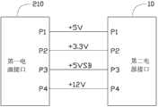
请参阅图1及图2,本发明较佳实施方式的电源容性负载测试装置100用于测试一PSU 200的各路电源的最大容性负载。PSU 200应用于计算机,用于输出多路电源给计算机的各个电源元件供电。多路电源可以分别为+5V电源、+3.3V电源、+5V备用电源以及+12V电源等。PSU 200包括第一电源接口210。电源容性负载测试装置100包括第二电源接口10、控制器20、电源选通电路30、电流采样电路40、容性负载选通电路50、放电电路60以及显示器70。Please refer to FIG. 1 and FIG. 2 , a power supply capacitiveload testing device 100 according to a preferred embodiment of the present invention is used to test the maximum capacitive load of each power supply of aPSU 200 . The PSU 200 is used in computers, and is used to output multiple power supplies to supply power to various power components of the computer. Multiple power supplies can be +5V power supply, +3.3V power supply, +5V backup power supply and +12V power supply, etc. The PSU 200 includes afirst power interface 210 . The power capacitiveload testing device 100 includes asecond power interface 10 , acontroller 20 , apower gating circuit 30 , acurrent sampling circuit 40 , a capacitiveload gating circuit 50 , adischarge circuit 60 and adisplay 70 .

请一并参阅图2,第一电源接口210包括+5V电源输出引脚P1、+3.3V电源输出引脚P2、5V备用电源输出引脚P3以及+12V电源输出引脚P4。+5V电源输出引脚P1、+3.3V电源输出引脚P2、5V备用电源输出引脚P3以及+12V电源输出引脚P4分别输出+5V电源、+3.3V电源、+5V备用电源(+5VSB)以及+12V电源。第一电源接口210为一二十四引脚(24 pin)的电源接口,图中只示出其中四个引脚。Please also refer to FIG. 2 , thefirst power interface 210 includes a +5V power output pin P1 , a +3.3V power output pin P2 , a 5V backup power output pin P3 and a +12V power output pin P4 . +5V power output pin P1, +3.3V power output pin P2, 5V backup power output pin P3 and +12V power output pin P4 respectively output +5V power, +3.3V power, +5V backup power (+5VSB ) and +12V power supply. Thefirst power interface 210 is a power interface with twenty-four pins (24 pins), of which only four pins are shown in the figure.

第二电源接口10用于将电源容性负载测试装置100电性连接至PSU,以接收所述+5V电源、+3.3V电源、+5V备用电源以及+12V电源。第二电源接口10具有与第一电源接口210相同的结构,第二电源接口10包括与第一电源接口210的+5V电源输出引脚P1、+3.3V电源输出引脚P2、+3.3V电源输出引脚P2、5V备用电源输出引脚P3以及+12V电源输出引脚P4一一对应连接的+5V电源输出引脚P1、+3.3V电源输出引脚P2、+3.3V电源输出引脚P2、5V备用电源输出引脚P3以及+12V电源输出引脚P4。Thesecond power interface 10 is used to electrically connect the power supply capacitiveload testing device 100 to the PSU to receive the +5V power supply, +3.3V power supply, +5V backup power supply and +12V power supply. Thesecond power interface 10 has the same structure as thefirst power interface 210, and thesecond power interface 10 includes the +5V power output pin P1, the +3.3V power output pin P2, and the +3.3V power supply of thefirst power interface 210. Output pin P2, 5V standby power output pin P3, and +12V power output pin P4 are connected one by one to +5V power output pin P1, +3.3V power output pin P2, +3.3V power output pin P2 , 5V standby power output pin P3 and +12V power output pin P4.

请参阅图3,控制器20用于控制电源选通电路30选择性地将PSU输出的多路电源中的其中一路电源连接至容性负载选通电路50,并控制容性负载选通电路50将不同的电容值的容性负载连接至被选通的电源;同时,控制器20还用于接收电流采样电路40采样的被选通的电源的输出电流,根据所述输出电流的大小判断被选通的电源所连接的容性负载是否达到其最大容性负载。Please refer to FIG. 3 , thecontroller 20 is used to control thepower gating circuit 30 to selectively connect one of the multiple power sources output by the PSU to the capacitiveload gating circuit 50 and control the capacitiveload gating circuit 50 Connect capacitive loads of different capacitance values to the gated power supply; at the same time, thecontroller 20 is also used to receive the output current of the gated power supply sampled by thecurrent sampling circuit 40, and judge the gated power supply according to the magnitude of the output current. Whether the gated power supply is connected to a capacitive load at its maximum capacitive load.

具体地,控制器20包括电性连接至电源选通电路30的电源选通引脚PD1-PD4、电性连接至容性负载选通电路的多个容性负载选通引脚PA1-PAn、电性连接至电流采样电路40的采样数据输入引脚PC1以及电性连接至放电电路60的放电控制引脚PB1。Specifically, thecontroller 20 includes power gating pins PD1-PD4 electrically connected to thepower gating circuit 30, a plurality of capacitive load gating pins PA1-PAn electrically connected to the capacitive load gating circuit, It is electrically connected to the sampling data input pin PC1 of thecurrent sampling circuit 40 and is electrically connected to the discharge control pin PB1 of thedischarge circuit 60 .

电源选通电路30包括与多路电源数量相同的多个第一选通开关,如图3中所示的第一选通开关31a、31b。每一第一选通开关包括输入端、输出端以及电性连接至控制器20的控制端。每一第一选通开关的输入端通过第二电源接口10电性连接至PSU 200的其中一个对应的电源,多个第一选通开关的输出端均电性连接至容性负载选通电路50以及电流采样电路40。控制器20通过控制第一选通开关的控制端使得所述输入端与输出端相互断开或相互连接,从而使得与该第一选通开关的所述输入端相连接的电源与容性负载选通电路50及电流采样电路40相互断开或相互连接。并且控制器20通过对多个第一选通开关的控制端的配合控制,可以使得每一次测试只选通其中一个第一选通开关,从而分别测试多路电源。Thepower gating circuit 30 includes a plurality of first gating switches equal to the number of multiple power sources, such as thefirst gating switches 31a and 31b shown in FIG. 3 . Each first gating switch includes an input terminal, an output terminal and a control terminal electrically connected to thecontroller 20 . The input end of each first gating switch is electrically connected to one of the corresponding power supplies of thePSU 200 through thesecond power interface 10, and the output ends of the plurality of first gating switches are electrically connected to the capacitive load gating circuit. 50 and thecurrent sampling circuit 40. Thecontroller 20 controls the control end of the first gating switch so that the input end and the output end are disconnected or connected to each other, so that the power supply connected to the input end of the first gating switch and the capacitive load Thegating circuit 50 and thecurrent sampling circuit 40 are disconnected or connected to each other. In addition, thecontroller 20 can enable only one of the first gating switches to be switched on for each test through cooperative control of the control terminals of the multiple first gating switches, so as to test multiple power sources respectively.

在本实施方式中,电源选通电路30还包括升压芯片33。所述升压芯片33用于将一输入电压(例如+5V电压)转换成一漏极电压。所述漏极电压大于多路电源中任何一个的电压。在本实施方式中,所述漏极电压的大小为+15V。In this embodiment, thepower gating circuit 30 further includes aboost chip 33 . Theboost chip 33 is used to convert an input voltage (eg +5V voltage) into a drain voltage. The drain voltage is greater than the voltage of any one of the multiple power supplies. In this embodiment, the magnitude of the drain voltage is +15V.

如图3所示,图3中只示出了两个第一选通开关31a、31b,分别用于选通+5V电源以及+3.3V电源,其它第一选通开关省略。第一选通开关31a包括第一金属氧化物半导体场效应晶体管(Metal-Oxide-Semiconductor Field-Effect Transistor, MOSFET)Q1及第二MOSFET Q2。MOSFET Q1的栅极g1电性连接至控制器20的电源选通引脚PD1,源极s1接地,漏极d1通过一第一上拉电阻R1电性连接至升压芯片33的输出端以接收+15V的漏极电压,第二MOSFET Q2的栅极g2电性连接至第一MOSFET Q1的漏极d2与第一上拉电阻R1之间,漏极d2电性连接至第二电源接口10的+5V电源引脚以接收+5V电源,源极s2电性连接至容性负载选通电路50以及电流采样电路40。如此,第一MOSFET Q1的栅极g1即为第一选通开关31a的所述控制端,第二MOSFET Q2的漏极d2即为第一选通开关31a的所述输入端,源极s2即为第一选通开关31a的所述输出端。第一选通开关31b具有与第一选通开关31a相同的结构,不同之处在于,第一选通开关31b的第一MOSFET Q1的栅极g1电性连接至控制器20的电源选通引脚PD2,第二MOSFET Q2的漏极d2电性连接至第二电源接口10的+3.3V电源引脚以接收+3.3V电源,第一选通开关31a及31b之间的节点为A,节点A即为所述电源选通电路30的输出端。As shown in FIG. 3 , only two first strobe switches 31 a and 31 b are shown in FIG. 3 , which are respectively used to strobe the +5V power supply and the +3.3V power supply, and the other first strobe switches are omitted. Thefirst gate switch 31a includes a first Metal-Oxide-Semiconductor Field-Effect Transistor (MOSFET) Q1 and a second MOSFET Q2. The gate g1 of MOSFET Q1 is electrically connected to the power selection pin PD1 of thecontroller 20, the source s1 is grounded, and the drain d1 is electrically connected to the output terminal of theboost chip 33 through a first pull-up resistor R1 to receive +15V drain voltage, the gate g2 of the second MOSFET Q2 is electrically connected between the drain d2 of the first MOSFET Q1 and the first pull-up resistor R1, and the drain d2 is electrically connected to thesecond power interface 10 The +5V power supply pin is used to receive the +5V power supply, and the source s2 is electrically connected to the capacitiveload gating circuit 50 and thecurrent sampling circuit 40 . In this way, the gate g1 of the first MOSFET Q1 is the control terminal of thefirst gate switch 31a, the drain d2 of the second MOSFET Q2 is the input terminal of thefirst gate switch 31a, and the source s2 is the is the output terminal of thefirst gate switch 31a. Thefirst gating switch 31b has the same structure as thefirst gating switch 31a, the difference is that the gate g1 of the first MOSFET Q1 of thefirst gating switch 31b is electrically connected to the power gating lead of thecontroller 20. Pin PD2, the drain d2 of the second MOSFET Q2 is electrically connected to the +3.3V power supply pin of the secondpower supply interface 10 to receive the +3.3V power supply, the node between thefirst strobe switch 31a and 31b is A, the node A is the output end of thepower gating circuit 30 .

若控制器20需要选通+5V电源,则控制器20通过电源选通引脚PD1输出一低电平(逻辑0)信号至第一选通开关31a的第一MOSFET Q1的栅极g1,并输出高电平(逻辑1)信号至第一选通开关31b及其它第一选通开关,此时第一选通开关31a的第一MOSFET Q1截止,第一选通开关31a的第二MOSFET Q2导通;同时第一选通开关31b的第一MOSFET Q1导通,第一选通开关31a的第二MOSFET Q2截止,节点A输出的电压为+5V。同理,当控制器20需要选通其它任何一个第一选通开关,如第一选通开关31b时,只需输出低电平至第一选通开关31b,而输出高电平至其它第一选通开关,即可使得节点A输出的电压为+3.3V。If thecontroller 20 needs to strobe the +5V power supply, thecontroller 20 outputs a low level (logic 0) signal to the gate g1 of the first MOSFET Q1 of thefirst strobe switch 31a through the power strobe pin PD1, and Output a high level (logic 1) signal to thefirst strobe switch 31b and other first strobe switches. At this time, the first MOSFET Q1 of thefirst strobe switch 31a is cut off, and the second MOSFET Q2 of thefirst strobe switch 31a At the same time, the first MOSFET Q1 of thefirst gating switch 31b is turned on, the second MOSFET Q2 of thefirst gating switch 31a is turned off, and the output voltage of node A is +5V. Similarly, when thecontroller 20 needs to strobe any other first strobe switch, such as thefirst strobe switch 31b, it only needs to output a low level to thefirst strobe switch 31b, and output a high level to the otherfirst strobe switch 31b. Once the switch is selected, the output voltage of node A can be +3.3V.

请参阅图4,电流采样电路40用于配合控制器20检测电源选通电路30所选通的电源的输出电流。电流采样电路40包括电流检测电阻R3、滤波电容C1及C2、电压采样放大单元41以及电性连接至电压采样放大单元41的模数转换芯片43。电流检测电阻R3串联至电源选通电路30的输出端,即节点A与容性负载选通电路50(如图5所示)之间。电流检测电阻R3一端通过滤波电容C1接地,另一端通过滤波电容C2接地。Please refer to FIG. 4 , thecurrent sampling circuit 40 is used to cooperate with thecontroller 20 to detect the output current of the power source selected by thepower gating circuit 30 . Thecurrent sampling circuit 40 includes a current detection resistor R3 , filter capacitors C1 and C2 , a voltage sampling and amplifyingunit 41 , and an analog-to-digital conversion chip 43 electrically connected to the voltage sampling and amplifyingunit 41 . The current detection resistor R3 is connected in series with the output end of thepower gating circuit 30 , that is, between the node A and the capacitive load gating circuit 50 (as shown in FIG. 5 ). One end of the current detection resistor R3 is grounded through the filter capacitor C1, and the other end is grounded through the filter capacitor C2.

电压采样放大单元41用于检测电流检测电阻R3两端的电压并将电流检测电阻R3两端的电压进行放大后输出至模数转换芯片43。在本实施方式中,电压采样放大单元41包括第一同相放大器411、第二同相放大器412、差值放大器413、增益设置电阻R4以及电阻R5-R9。第一同相放大器411及第二同相放大器412的同相输入端分别电性连接至电流检测电阻R3的两端,第一同相放大器411及第二同相放大器412的反相输入端通过增益设置电阻R4连接于一起。第一同相放大器411的输出端通过电阻R7电性连接至差值放大器413的反相相输入端,第二同相放大器412的输出端通过电阻R8电性连接至差值放大器413的同相输入端。电阻R5电性连接至第一同相放大器411的输出端与反相输入端之间;电阻R6电性连接至第二同相放大器412的输出端与反相输入端之间;电阻R9电性连接至差值放大器413的输出端与反相输入端之间。第一同相放大器411及第二同相放大器412组成对称的同相放大器,分别用于对电流检测电阻R3两端的电压进行放大,并将放大后的电压分别输出至差值放大器413的反相输入端及同相输入端。差值放大器413再将其同相输入端的电压与反相输入端的电压的差值进行放大后输出至模数转换芯片43。整个电压采样放大单元41的放大倍数可以通过增益设置电阻R4进行调节。The voltage sampling and amplifyingunit 41 is used to detect the voltage across the current detection resistor R3 and amplify the voltage across the current detection resistor R3 to output to the analog-to-digital conversion chip 43 . In this embodiment, the voltage sampling and amplifyingunit 41 includes a firstnon-inverting amplifier 411, a secondnon-inverting amplifier 412, adifference amplifier 413, a gain setting resistor R4, and resistors R5-R9. The non-inverting input terminals of the firstnon-inverting amplifier 411 and the secondnon-inverting amplifier 412 are respectively electrically connected to the two ends of the current detection resistor R3, and the inverting input terminals of the firstnon-inverting amplifier 411 and the second non-invertingamplifier 412 pass through the gain setting resistor R4 are connected together. The output terminal of the firstnon-inverting amplifier 411 is electrically connected to the inverting input terminal of thedifference amplifier 413 through the resistor R7, and the output terminal of the secondnon-inverting amplifier 412 is electrically connected to the non-inverting input terminal of thedifference amplifier 413 through the resistor R8 . The resistor R5 is electrically connected between the output terminal and the inverting input terminal of the firstnon-inverting amplifier 411; the resistor R6 is electrically connected between the output terminal and the inverting input terminal of the secondnon-inverting amplifier 412; the resistor R9 is electrically connected Between the output terminal of thedifference amplifier 413 and the inverting input terminal. The firstnon-inverting amplifier 411 and the secondnon-inverting amplifier 412 form a symmetrical non-inverting amplifier, which are respectively used to amplify the voltage at both ends of the current detection resistor R3, and output the amplified voltage to the inverting input terminal of thedifference amplifier 413 respectively and non-inverting input. Thedifference amplifier 413 amplifies the difference between the voltage at the non-inverting input terminal and the voltage at the inverting input terminal, and then outputs it to the analog-to-digital conversion chip 43 . The amplification factor of the entire voltagesampling amplifying unit 41 can be adjusted through the gain setting resistor R4.

模数转换芯片43用于将电压采样放大单元41采样到的模拟电压信号转换为数字电压信号后,输出至控制器20的采样数据输入引脚PC1。控制器20则将接收到的数字电压信号除以所述电流检测电阻R3的阻值以及电压采样放大单元41的放大倍数,则可得到电源选通电路30所选通的电源的输出电流的值。控制器20将所述输出电流的值与一参考电流值进行比较,其中,所述参考电流值为被选通的电源发生过流保护时的电流值。The analog-to-digital conversion chip 43 is used to convert the analog voltage signal sampled by the voltage sampling and amplifyingunit 41 into a digital voltage signal, and then output it to the sampling data input pin PC1 of thecontroller 20 . Thecontroller 20 divides the received digital voltage signal by the resistance value of the current detection resistor R3 and the amplification factor of the voltagesampling amplifying unit 41, and then the value of the output current of the power source selected by thepower gating circuit 30 can be obtained. . Thecontroller 20 compares the value of the output current with a reference current value, wherein the reference current value is the current value when the over-current protection of the gated power supply occurs.

请参阅图5,容性负载选通电路50包括与控制器20的容性负载选通引脚PA1-PAn数量相同且一一对应的第二选通开关(如图5中所示的第二选通开关51a、51b)及与第二选通开关数量相同且一一对应的多个负载电容(如图5中所示的负载电容C3、C4)。每一第二选通开关电性连接至控制器20的对应的容性负载选通引脚。每一负载电容的正极均通过电流检测电阻R3电性连接至电源选通电路30的输出端,负极通过对应的所述第二选通开关连接至地。控制器20通过控制多个所述第二选通开关的通断即可相应地建立或断开与多个第二选通开关分别对应的负载电容与电源选通电路30所选通的电源之间的连接,从而将不同电容总值的负载电容接入被选通的电源。Referring to FIG. 5 , the capacitiveload gating circuit 50 includes a second gating switch with the same number and one-to-one correspondence with the capacitive load gating pins PA1-PAn of the controller 20 (as shown in FIG. gating switches 51 a , 51 b ) and a plurality of load capacitors (load capacitors C3 , C4 shown in FIG. 5 ) having the same number as the second gating switches and one-to-one correspondence. Each second gate switch is electrically connected to a corresponding capacitive load gate pin of thecontroller 20 . The anode of each load capacitor is electrically connected to the output terminal of thepower gating circuit 30 through the current detection resistor R3, and the cathode is connected to the ground through the corresponding second gating switch. Thecontroller 20 can correspondingly establish or disconnect the connection between the load capacitance corresponding to the plurality of second gating switches and the power source selected by thepower gating circuit 30 by controlling the on-off of the plurality of second gating switches. The connection between them, so that the load capacitors with different total capacitance values are connected to the power supply to be gated.

具体地,请参阅图5,图5中以第二选通开关51a、51b以及负载电容C3、C4为例进行说明。第二选通开关51a包括第三MOSFET Q3以及第二MOSFET Q4。第三MOSFET Q3的栅极g3电性连接至控制器20的容性负载选通引脚PA1,漏极d3通过一第二上拉电阻R2电性连接至升压芯片33的输出端以接收+15V的漏极电压,源极s3接地。第四MOSFET Q4的栅极g4电性连接至漏极d3与第二上拉电阻R2之间,漏极d4通过对应的负载电容C3电性连接至电源选通电路30的输出端,源极s4接地。第二选通开关51b具有与第二选通开关51a相同的结构,不同之处在于,第二选通开关51b的第一MOSFET Q3的栅极g3电性连接至控制器20的容性负载选通引脚PAn,第二选通开关51b的第二MOSFET Q4的漏极d4通过负载电容C4连接至电源选通电路30的输出端。Specifically, please refer to FIG. 5 . In FIG. 5 , thesecond gating switches 51a, 51b and the load capacitors C3, C4 are taken as examples for illustration. Thesecond gate switch 51a includes a third MOSFET Q3 and a second MOSFET Q4. The gate g3 of the third MOSFET Q3 is electrically connected to the capacitive load selection pin PA1 of thecontroller 20, and the drain d3 is electrically connected to the output terminal of theboost chip 33 through a second pull-up resistor R2 to receive + Drain voltage of 15V, source s3 grounded. The gate g4 of the fourth MOSFET Q4 is electrically connected between the drain d3 and the second pull-up resistor R2, the drain d4 is electrically connected to the output terminal of thepower gating circuit 30 through the corresponding load capacitor C3, and the source s4 grounded. Thesecond gating switch 51b has the same structure as thesecond gating switch 51a, the difference is that the gate g3 of the first MOSFET Q3 of thesecond gating switch 51b is electrically connected to the capacitive load selection of thecontroller 20. Through the pin PAn, the drain d4 of the second MOSFET Q4 of thesecond gating switch 51b is connected to the output terminal of thepower gating circuit 30 through the load capacitor C4.

当控制器20对选通的电源,例如+5V电源进行容性负载测试时,控制器20首先通过容性负载选通引脚PA1输出一低电平信号选通第二选通开关51a,使负载电容C3接入所述+5V电源,若控制器20通过检测+5V电源的输出电流的值小于所述参考电流值,所述控制器20则依次选通剩下的第二选通开关,容性负载选通电路50逐渐选通更多的负载电容,直至所述输出电流的值等于所述参考电流的值,即接入+5V电源的负载电容的总的电容值达到+5V电源的最大容性负载值为止。控制器20可根据所选通的第二选通开关对应的负载电容的电容值统计总的电容值。可以理解,多个负载电容的电容值可以按照选通的先后顺序依次增大。When thecontroller 20 performs a capacitive load test on the selected power supply, such as +5V power supply, thecontroller 20 first outputs a low-level signal through the capacitive load selection pin PA1 to select thesecond selection switch 51a, so that The load capacitor C3 is connected to the +5V power supply, and if thecontroller 20 detects that the output current value of the +5V power supply is smaller than the reference current value, thecontroller 20 sequentially selects the remaining second gate switches, The capacitiveload gating circuit 50 gradually gating more load capacitors until the value of the output current is equal to the value of the reference current, that is, the total capacitance value of the load capacitors connected to the +5V power supply reaches that of the +5V power supply. up to the maximum capacitive load value. Thecontroller 20 can calculate the total capacitance value according to the capacitance value of the load capacitance corresponding to the selected second gate switch. It can be understood that the capacitance values of the multiple load capacitors may increase sequentially according to the sequence of the gates.

可以理解,为了避免控制器20统计的最大容性负载值的精确度造成影响,滤波电容C1以及C2的电容值较佳地小于或等于1纳法,在本实施方式中为1纳法;电流检测电阻R3的阻值低于0.1欧姆,在本实施方式中为0.04欧姆。It can be understood that, in order to avoid the impact on the accuracy of the maximum capacitive load value counted by thecontroller 20, the capacitance values of the filter capacitors C1 and C2 are preferably less than or equal to 1 nanofarad, which is 1 nanofarad in this embodiment; The resistance value of the detection resistor R3 is lower than 0.1 ohm, and is 0.04 ohm in this embodiment.

放电电路60电性连接至控制器20,用于在每一所述电源完成后,对多个所述负载电容进行放电,以提高测试精度。所述放电电路60包括第五MOSFET Q5以及放电电阻R10。第五MOSFET Q5的栅极g5电性连接至控制器20的放电控制引脚PB1,源极s5,漏极d5通过放电电阻R10电性连接至每一所述负载电容的正极。当控制器20完成对其中一路电源的最大容性负载测试后,则通过放电控制引脚PB1发送一低电平信号至第五MOSFET Q5使其导通,多个所述负载电容,如负载电容C3、C2上的电量则通过所述放电电阻R10接地释放。可以理解,为了避免较大的放电电流对第五MOSFET Q5造成损害,放电电路60还可以包括多个MOSFET及多个放电电阻,每一MOSFET的栅极电性连接至控制器20的放电控制引脚PB1,源极接地,漏极通过其中一个对应的放电电阻电性连接至多个负载电容的正极,如此,在放电时,多个放电电阻可对放电电流进行分流,降低对MOSFET的损害。Thedischarge circuit 60 is electrically connected to thecontroller 20, and is used for discharging a plurality of the load capacitors after each power supply is completed, so as to improve test accuracy. Thedischarge circuit 60 includes a fifth MOSFET Q5 and a discharge resistor R10. The gate g5 of the fifth MOSFET Q5 is electrically connected to the discharge control pin PB1 of thecontroller 20, the source s5, and the drain d5 are electrically connected to the anode of each of the load capacitors through the discharge resistor R10. After thecontroller 20 completes the maximum capacitive load test to one of the power supplies, it sends a low-level signal to the fifth MOSFET Q5 through the discharge control pin PB1 to make it turn on, and multiple load capacitors, such as load capacitors The electricity on C3 and C2 is grounded and discharged through the discharge resistor R10. It can be understood that, in order to avoid damage to the fifth MOSFET Q5 caused by a large discharge current, thedischarge circuit 60 may also include a plurality of MOSFETs and a plurality of discharge resistors, and the gate of each MOSFET is electrically connected to the discharge control lead of thecontroller 20. Pin PB1, the source is grounded, and the drain is electrically connected to the positive poles of multiple load capacitors through one of the corresponding discharge resistors. In this way, when discharging, multiple discharge resistors can shunt the discharge current to reduce damage to the MOSFET.

所述显示器70电性连接至控制器20,用于对控制器20测得的各电源的最大容性负载值进行显示。Thedisplay 70 is electrically connected to thecontroller 20 for displaying the maximum capacitive load value of each power source measured by thecontroller 20 .

所述的电源容性负载测试装置100通过所述电源选通电路30选择性地依次选通多个电源中一路进行最大容性负载测试,通过控制器20控制容性负载选通电路50将不同电容总值的负载电容接入被选通的电源,并判断接入被选通电源的电容总值是否到达其最大容性负载值。如此,不仅可准确地测试被选通电源的最大容性负载,还可完成对PSU 200的输出的各路电源进行容性负载测试。The power supply capacitiveload testing device 100 selectively selects one way in a plurality of power supplies to carry out the maximum capacitive load test through thepower gating circuit 30, and the capacitiveload gating circuit 50 is controlled by thecontroller 20. The load capacitance of the total value of the capacitance is connected to the gated power supply, and it is judged whether the total value of the capacitance connected to the gated power supply reaches its maximum capacitive load value. In this way, not only the maximum capacitive load of the gated power supply can be accurately tested, but also the capacitive load test of each power supply output by thePSU 200 can be completed.

Claims (10)

1. power supply capacitive load proving installation, the maximum capacitive load value that is used for the multiple power supplies of test one supply unit output, it is characterized in that: described power supply capacitive load proving installation comprises controller and the power supply gating circuit that all is connected with described controller, capacitive load gating circuit and current sampling circuit, described power supply gating circuit is electrically connected to described multiple power supplies, capacitive load gating circuit and current sampling circuit are used under the control of described controller optionally wherein one road power supply of described multiple power supplies is connected to capacitive load gating circuit and current sampling circuit; Described capacitive load gating circuit comprises a plurality of load capacitances; Described current sampling circuit is for the output current of the described power supply that cooperates described controller sampling to be strobed; Described controller is used for described output current and a reference current are compared, control described capacitive load gating circuit and optionally one or more in a plurality of load capacitances are connected in parallel to the described power supply that is strobed until described output current is identical with reference current, and the electric capacity total value of a plurality of load capacitances of output institute gating.
2. power supply capacitive load proving installation as claimed in claim 1, it is characterized in that: described power supply gating circuit comprises a plurality of first gating switches identical with described multiple power supplies quantity, each described first gating switch comprises input end, output terminal and the control end that is electrically connected to described controller, the input end of each described the first gating switch is electrically connected to a corresponding described power supply, the output terminal of a plurality of described the first gating switches all is electrically connected to described capacitive load gating circuit and described current sampling circuit, described controller by controlling respectively a plurality of described the first gating switches input end and output terminal between interconnect or disconnect, realize the gating to corresponding described power supply.
3. power supply capacitive load proving installation as claimed in claim 2, it is characterized in that: each described first gating switch comprises the first mos field effect transistor and the second mos field effect transistor, the grid of described the first mos field effect transistor is electrically connected to described controller, source ground, drain electrode is electrically connected to a drain voltage; The grid of described the second mos field effect transistor is electrically connected to the drain electrode of the first mos field effect transistor, the drain electrode of described the second mos field effect transistor is electrically connected to one of them power supply in described a plurality of power supply, and the source electrode of described the second mos field effect transistor is electrically connected to described capacitive load gating circuit and described current sampling circuit.
5. power supply capacitive load proving installation as claimed in claim 1, it is characterized in that: described capacitive load gating circuit comprises a plurality of second gating switches identical with a plurality of load capacitance quantity, each described second gating switch all is electrically connected to controller, the positive pole of each described load capacitance all is electrically connected to the output terminal of described power supply gating circuit, negative pole is connected to ground by the second gating switch of correspondence, described controller can correspondingly be set up by the break-make of controlling a plurality of described the second gating switches or disconnection and a plurality of the second gating switches being connected between the power supply of corresponding load capacitance and power supply gating circuit institute gating respectively, thereby the load capacitance of different electric capacity total values is accessed the power supply that is strobed.
7. power supply capacitive load proving installation as claimed in claim 1, it is characterized in that: described current sampling circuit comprises current sense resistor, voltage sample amplifying unit and modulus conversion chip, described current sense resistor is connected serially between the output terminal and described capacitive load gating circuit of described power supply gating circuit, described voltage sample amplifying unit exports modulus conversion chip to after amplifying for detection of the voltage at described current sense resistor two ends and with this voltage, described voltage transitions after described modulus conversion chip is used for amplifying becomes the described controller of digital voltage value output valve, described controller divided by the resistance of described current sense resistor and the enlargement factor of described voltage sample amplifying unit, namely obtains the output current value of the described power supply that is strobed with the digital voltage value that receives.
8. power supply capacitive load proving installation as claimed in claim 1, it is characterized in that: described voltage sample amplifying unit comprises that the first in-phase amplifier, the second in-phase amplifier, difference amplifier and gain arrange resistance; The in-phase input end of described the first in-phase amplifier and the second in-phase amplifier is electrically connected to respectively the two ends of described current sense resistor, and the inverting input of described the first in-phase amplifier and the second in-phase amplifier arranges resistance by gain and is connected together; The output terminal of described the first in-phase amplifier is electrically connected to the anti-phase phase input end of described difference amplifier, and the output terminal of described the second in-phase amplifier is electrically connected to the in-phase input end of described difference amplifier; Described the first in-phase amplifier and the second in-phase amplifier form symmetrical in-phase amplifier, be respectively applied to the voltage at described current sense resistor two ends is amplified, and the voltage after will amplifying exports respectively inverting input and the in-phase input end of described difference amplifier to; Described difference amplifier exports described modulus conversion chip to after the difference of the voltage of the voltage of its in-phase input end and inverting input being amplified again.
9. power supply capacitive load proving installation as claimed in claim 1, it is characterized in that: described power supply capacitive load proving installation also comprises discharge circuit, described discharge circuit comprises that five metals belongs to oxide semiconductor field effect transistor and discharge resistance, the grid that five metals belongs to oxide semiconductor field effect transistor is electrically connected to controller, source ground, drain electrode is electrically connected to the positive pole of each load capacitance by described discharge resistance, described controller is behind the maximum capacitive load testing of finishing each described power supply, belong to the oxide semiconductor field effect transistor conducting by controlling described five metals, thereby so that the electric weight on each load capacitance passes through described discharge resistance discharge.
CN2012100813351A2012-03-262012-03-26Power capacitive-load testing devicePendingCN103364737A (en)

Priority Applications (3)

Application NumberPriority DateFiling DateTitle
CN2012100813351ACN103364737A (en)2012-03-262012-03-26Power capacitive-load testing device
TW101111598ATW201339610A (en)2012-03-262012-03-30Power supply condensive load testing device
US13/736,989US8933704B2 (en)2012-03-262013-01-09Capacitive load testing device of power supply

Applications Claiming Priority (1)

Application NumberPriority DateFiling DateTitle
CN2012100813351ACN103364737A (en)2012-03-262012-03-26Power capacitive-load testing device

Publications (1)

Publication NumberPublication Date
CN103364737Atrue CN103364737A (en)2013-10-23

Family

ID=49211196

Family Applications (1)

Application NumberTitlePriority DateFiling Date
CN2012100813351APendingCN103364737A (en)2012-03-262012-03-26Power capacitive-load testing device

Country Status (3)

CountryLink
US (1)US8933704B2 (en)
CN (1)CN103364737A (en)
TW (1)TW201339610A (en)

Cited By (3)

* Cited by examiner, † Cited by third party
Publication numberPriority datePublication dateAssigneeTitle
CN104408998A (en)*2014-12-022015-03-11国家电网公司Electrical running simulation device of capacitive equipment
CN107222023A (en)*2017-07-272017-09-29郑州云海信息技术有限公司Reserve battery power supply circuit, the battery status monitoring of reserve battery and calibration method
CN118707407A (en)*2024-08-292024-09-27苏州元脑智能科技有限公司 Capacitive load testing system, method, electronic device, storage medium and product

Families Citing this family (3)

* Cited by examiner, † Cited by third party
Publication numberPriority datePublication dateAssigneeTitle
US9030225B2 (en)*2013-05-022015-05-12Chicony Power Technology Co., Ltd.Over voltage protection testing apparatus
CN109787635A (en)*2019-01-102019-05-21京东方科技集团股份有限公司D/A converting circuit and its digital-analog convertion method, display device
CN114062960A (en)*2021-11-162022-02-18河北凯翔电气科技股份有限公司 A data center backup power test system and its test method

Citations (6)

* Cited by examiner, † Cited by third party
Publication numberPriority datePublication dateAssigneeTitle
US5397999A (en)*1991-08-091995-03-14Pfu LimitedEvaluation apparatus for power supply system
US6366063B1 (en)*2000-03-222002-04-02Nec CorporationCircuit and method for driving capacitive load
CN101907689A (en)*2010-06-302010-12-08中兴通讯股份有限公司 Test circuit generation method, device and power supply test system
CN101930025A (en)*2009-06-222010-12-29研祥智能科技股份有限公司Power dissipation testing device
CN201742140U (en)*2010-06-282011-02-09山东申普汽车控制技术有限公司Harmless quick balanced charger for storage batteries
CN102262193A (en)*2011-06-132011-11-30深圳市普联技术有限公司Circuit and method for testing capacitive load

Family Cites Families (13)

* Cited by examiner, † Cited by third party
Publication numberPriority datePublication dateAssigneeTitle
DE10349072B3 (en)*2003-10-142005-02-03Msa Auer GmbhSwitching in current limiting circuit for electronic module fitted in rack, using comparator for comparing reference voltage with operating voltage supplied via charging capacitors defining switching in delay
US7851946B2 (en)*2004-10-192010-12-14Rohm Co., Ltd.Switching power supply and electronic apparatus employing the same
TW200624826A (en)*2004-10-292006-07-16Koninkl Philips Electronics NvSystem for diagnosing impedances having accurate current source and accurate voltage level-shift
US7057397B1 (en)*2005-03-032006-06-06Lattice Semiconductor CorporationOutput impedance measurement techniques
US8198756B2 (en)*2006-10-262012-06-12Nxp B.V.Voltage-boosting stage
JP4210867B2 (en)*2006-12-272009-01-21ソニー株式会社 Variable capacitance circuit
US7656061B2 (en)*2007-10-292010-02-02Bose CorporationAutomatic power source configuration
EP2446525B1 (en)*2009-06-252018-12-19Flex, Ltd.Capacitance determination in a switched mode power supply
US8638010B2 (en)*2010-02-172014-01-28Integrated Device Technology, Inc.Systems, devices, and methods for providing backup power to a load
US8193787B2 (en)*2010-07-062012-06-05V Square/R, LLCSystem and method for regulating RMS voltage delivered to a load
DE102011009474A1 (en)*2011-01-262012-07-26Liebherr-Elektronik Gmbh Apparatus and method for monitoring and balancing a multicell energy storage stack
US8310098B2 (en)*2011-05-162012-11-13Unigen CorporationSwitchable capacitor arrays for preventing power interruptions and extending backup power life
US8531324B2 (en)*2011-07-192013-09-10Freescale Semiconductor, Inc.Systems and methods for data conversion

Patent Citations (6)

* Cited by examiner, † Cited by third party
Publication numberPriority datePublication dateAssigneeTitle
US5397999A (en)*1991-08-091995-03-14Pfu LimitedEvaluation apparatus for power supply system
US6366063B1 (en)*2000-03-222002-04-02Nec CorporationCircuit and method for driving capacitive load
CN101930025A (en)*2009-06-222010-12-29研祥智能科技股份有限公司Power dissipation testing device
CN201742140U (en)*2010-06-282011-02-09山东申普汽车控制技术有限公司Harmless quick balanced charger for storage batteries
CN101907689A (en)*2010-06-302010-12-08中兴通讯股份有限公司 Test circuit generation method, device and power supply test system
CN102262193A (en)*2011-06-132011-11-30深圳市普联技术有限公司Circuit and method for testing capacitive load

Cited By (4)

* Cited by examiner, † Cited by third party
Publication numberPriority datePublication dateAssigneeTitle
CN104408998A (en)*2014-12-022015-03-11国家电网公司Electrical running simulation device of capacitive equipment
CN107222023A (en)*2017-07-272017-09-29郑州云海信息技术有限公司Reserve battery power supply circuit, the battery status monitoring of reserve battery and calibration method
CN118707407A (en)*2024-08-292024-09-27苏州元脑智能科技有限公司 Capacitive load testing system, method, electronic device, storage medium and product
CN118707407B (en)*2024-08-292024-12-27苏州元脑智能科技有限公司Capacitive load test system, capacitive load test method, electronic device, storage medium and capacitive load test product

Also Published As

Publication numberPublication date
US20130249567A1 (en)2013-09-26
US8933704B2 (en)2015-01-13
TW201339610A (en)2013-10-01

Similar Documents

PublicationPublication DateTitle
CN110429673B (en) A power supply system, method, chip and terminal device for terminal equipment
CN103364737A (en)Power capacitive-load testing device
TW201403078A (en)Resistance testing apparatus
CN103229063A (en)Ground fault detection device, ground fault detection method, solar energy generator system, and ground fault detection program
CN103683348B (en)There is the electronic installation of power consumption detecting function
US9236752B2 (en)Method and system for voltage collapse protection
CN103091590B (en)A kind of series capacitance detection method and equipment
CN103080758A (en)Ground fault detection circuit for ungrounded power source
EP1118865A1 (en)Circuit and method for detecting load impedance
CN102541367B (en)A kind of capacitance-type touch control detection circuit, pick-up unit
CN103454572A (en)Battery analog circuit
CN109828173A (en)A kind of load-detecting system and its load detection method
CN101719757A (en)Over-current protection circuit of power amplifier and implementing method
US20130328405A1 (en)Ground test circuit
CN102098368B (en)Mobile phone
CN103529319B (en)Li-ion cell protection board test system
CN114720907A (en)Electric leakage detection device and system
CN103457302A (en)Charge circuit and electronic device with same
US20100181967A1 (en)Battery Charger and Associated Method
CN200976023Y (en)CMOS battery voltage detecting circuit
CN101995519B (en)Device and method for testing common-mode input impedance of operation amplifier
JP2022051714A (en)Voltage isolation circuit
CN113169385B (en)Battery pack, circuit system for measuring battery current and equipment for measuring battery current
CN216927045U (en)Detection circuit and polarity discrimination device
CN112180265A (en) battery tester

Legal Events

DateCodeTitleDescription
C06Publication
PB01Publication
C10Entry into substantive examination
SE01Entry into force of request for substantive examination
C02Deemed withdrawal of patent application after publication (patent law 2001)
WD01Invention patent application deemed withdrawn after publication

Application publication date:20131023


[8]ページ先頭

©2009-2025 Movatter.jp