CN103354818A - Compositions and methods for depositing conductive polymers on dielectric substrates - Google Patents
Compositions and methods for depositing conductive polymers on dielectric substratesDownload PDFInfo
- Publication number
- CN103354818A CN103354818ACN2011800637974ACN201180063797ACN103354818ACN 103354818 ACN103354818 ACN 103354818ACN 2011800637974 ACN2011800637974 ACN 2011800637974ACN 201180063797 ACN201180063797 ACN 201180063797ACN 103354818 ACN103354818 ACN 103354818A
- Authority
- CN
- China
- Prior art keywords
- ions
- composition
- conductive polymer
- acid
- copper
- Prior art date
- Legal status (The legal status is an assumption and is not a legal conclusion. Google has not performed a legal analysis and makes no representation as to the accuracy of the status listed.)
- Granted
Links
- 0*C1C(*)=C*C1Chemical compound*C1C(*)=C*C10.000description1
Images
Classifications
- C—CHEMISTRY; METALLURGY
- C08—ORGANIC MACROMOLECULAR COMPOUNDS; THEIR PREPARATION OR CHEMICAL WORKING-UP; COMPOSITIONS BASED THEREON
- C08G—MACROMOLECULAR COMPOUNDS OBTAINED OTHERWISE THAN BY REACTIONS ONLY INVOLVING UNSATURATED CARBON-TO-CARBON BONDS
- C08G61/00—Macromolecular compounds obtained by reactions forming a carbon-to-carbon link in the main chain of the macromolecule
- C08G61/12—Macromolecular compounds containing atoms other than carbon in the main chain of the macromolecule
- H—ELECTRICITY
- H05—ELECTRIC TECHNIQUES NOT OTHERWISE PROVIDED FOR
- H05K—PRINTED CIRCUITS; CASINGS OR CONSTRUCTIONAL DETAILS OF ELECTRIC APPARATUS; MANUFACTURE OF ASSEMBLAGES OF ELECTRICAL COMPONENTS
- H05K1/00—Printed circuits
- H05K1/02—Details
- H05K1/09—Use of materials for the conductive, e.g. metallic pattern
- H05K1/092—Dispersed materials, e.g. conductive pastes or inks
- H05K1/095—Dispersed materials, e.g. conductive pastes or inks for polymer thick films, i.e. having a permanent organic polymeric binder
- C—CHEMISTRY; METALLURGY
- C08—ORGANIC MACROMOLECULAR COMPOUNDS; THEIR PREPARATION OR CHEMICAL WORKING-UP; COMPOSITIONS BASED THEREON
- C08G—MACROMOLECULAR COMPOUNDS OBTAINED OTHERWISE THAN BY REACTIONS ONLY INVOLVING UNSATURATED CARBON-TO-CARBON BONDS
- C08G61/00—Macromolecular compounds obtained by reactions forming a carbon-to-carbon link in the main chain of the macromolecule
- C08G61/12—Macromolecular compounds containing atoms other than carbon in the main chain of the macromolecule
- C08G61/122—Macromolecular compounds containing atoms other than carbon in the main chain of the macromolecule derived from five- or six-membered heterocyclic compounds, other than imides
- C08G61/123—Macromolecular compounds containing atoms other than carbon in the main chain of the macromolecule derived from five- or six-membered heterocyclic compounds, other than imides derived from five-membered heterocyclic compounds
- C08G61/126—Macromolecular compounds containing atoms other than carbon in the main chain of the macromolecule derived from five- or six-membered heterocyclic compounds, other than imides derived from five-membered heterocyclic compounds with a five-membered ring containing one sulfur atom in the ring
- C—CHEMISTRY; METALLURGY
- C08—ORGANIC MACROMOLECULAR COMPOUNDS; THEIR PREPARATION OR CHEMICAL WORKING-UP; COMPOSITIONS BASED THEREON
- C08K—Use of inorganic or non-macromolecular organic substances as compounding ingredients
- C08K3/00—Use of inorganic substances as compounding ingredients
- C08K3/10—Metal compounds
- C—CHEMISTRY; METALLURGY
- C08—ORGANIC MACROMOLECULAR COMPOUNDS; THEIR PREPARATION OR CHEMICAL WORKING-UP; COMPOSITIONS BASED THEREON
- C08L—COMPOSITIONS OF MACROMOLECULAR COMPOUNDS
- C08L65/00—Compositions of macromolecular compounds obtained by reactions forming a carbon-to-carbon link in the main chain; Compositions of derivatives of such polymers
- C—CHEMISTRY; METALLURGY
- C25—ELECTROLYTIC OR ELECTROPHORETIC PROCESSES; APPARATUS THEREFOR
- C25D—PROCESSES FOR THE ELECTROLYTIC OR ELECTROPHORETIC PRODUCTION OF COATINGS; ELECTROFORMING; APPARATUS THEREFOR
- C25D5/00—Electroplating characterised by the process; Pretreatment or after-treatment of workpieces
- C25D5/54—Electroplating of non-metallic surfaces
- C25D5/56—Electroplating of non-metallic surfaces of plastics
- H—ELECTRICITY
- H01—ELECTRIC ELEMENTS
- H01B—CABLES; CONDUCTORS; INSULATORS; SELECTION OF MATERIALS FOR THEIR CONDUCTIVE, INSULATING OR DIELECTRIC PROPERTIES
- H01B1/00—Conductors or conductive bodies characterised by the conductive materials; Selection of materials as conductors
- H01B1/06—Conductors or conductive bodies characterised by the conductive materials; Selection of materials as conductors mainly consisting of other non-metallic substances
- H01B1/12—Conductors or conductive bodies characterised by the conductive materials; Selection of materials as conductors mainly consisting of other non-metallic substances organic substances
- H01B1/124—Intrinsically conductive polymers
- H01B1/127—Intrinsically conductive polymers comprising five-membered aromatic rings in the main chain, e.g. polypyrroles, polythiophenes
- H—ELECTRICITY
- H05—ELECTRIC TECHNIQUES NOT OTHERWISE PROVIDED FOR
- H05K—PRINTED CIRCUITS; CASINGS OR CONSTRUCTIONAL DETAILS OF ELECTRIC APPARATUS; MANUFACTURE OF ASSEMBLAGES OF ELECTRICAL COMPONENTS
- H05K3/00—Apparatus or processes for manufacturing printed circuits
- H05K3/40—Forming printed elements for providing electric connections to or between printed circuits
- H05K3/42—Plated through-holes or plated via connections
- H05K3/423—Plated through-holes or plated via connections characterised by electroplating method
- H05K3/424—Plated through-holes or plated via connections characterised by electroplating method by direct electroplating
- H—ELECTRICITY
- H05—ELECTRIC TECHNIQUES NOT OTHERWISE PROVIDED FOR
- H05K—PRINTED CIRCUITS; CASINGS OR CONSTRUCTIONAL DETAILS OF ELECTRIC APPARATUS; MANUFACTURE OF ASSEMBLAGES OF ELECTRICAL COMPONENTS
- H05K3/00—Apparatus or processes for manufacturing printed circuits
- H05K3/46—Manufacturing multilayer circuits
- H05K3/4644—Manufacturing multilayer circuits by building the multilayer layer by layer, i.e. build-up multilayer circuits
- H—ELECTRICITY
- H05—ELECTRIC TECHNIQUES NOT OTHERWISE PROVIDED FOR
- H05K—PRINTED CIRCUITS; CASINGS OR CONSTRUCTIONAL DETAILS OF ELECTRIC APPARATUS; MANUFACTURE OF ASSEMBLAGES OF ELECTRICAL COMPONENTS
- H05K2201/00—Indexing scheme relating to printed circuits covered by H05K1/00
- H05K2201/03—Conductive materials
- H05K2201/032—Materials
- H05K2201/0329—Intrinsically conductive polymer [ICP]; Semiconductive polymer
- H—ELECTRICITY
- H05—ELECTRIC TECHNIQUES NOT OTHERWISE PROVIDED FOR
- H05K—PRINTED CIRCUITS; CASINGS OR CONSTRUCTIONAL DETAILS OF ELECTRIC APPARATUS; MANUFACTURE OF ASSEMBLAGES OF ELECTRICAL COMPONENTS
- H05K3/00—Apparatus or processes for manufacturing printed circuits
- H05K3/02—Apparatus or processes for manufacturing printed circuits in which the conductive material is applied to the surface of the insulating support and is thereafter removed from such areas of the surface which are not intended for current conducting or shielding
- H05K3/022—Processes for manufacturing precursors of printed circuits, i.e. copper-clad substrates
- H—ELECTRICITY
- H05—ELECTRIC TECHNIQUES NOT OTHERWISE PROVIDED FOR
- H05K—PRINTED CIRCUITS; CASINGS OR CONSTRUCTIONAL DETAILS OF ELECTRIC APPARATUS; MANUFACTURE OF ASSEMBLAGES OF ELECTRICAL COMPONENTS
- H05K3/00—Apparatus or processes for manufacturing printed circuits
- H05K3/40—Forming printed elements for providing electric connections to or between printed circuits
- H05K3/42—Plated through-holes or plated via connections
- H05K3/425—Plated through-holes or plated via connections characterised by the sequence of steps for plating the through-holes or via connections in relation to the conductive pattern
- H05K3/427—Plated through-holes or plated via connections characterised by the sequence of steps for plating the through-holes or via connections in relation to the conductive pattern initial plating of through-holes in metal-clad substrates
Landscapes
- Chemical & Material Sciences (AREA)
- Engineering & Computer Science (AREA)
- Chemical Kinetics & Catalysis (AREA)
- Organic Chemistry (AREA)
- Microelectronics & Electronic Packaging (AREA)
- Health & Medical Sciences (AREA)
- Polymers & Plastics (AREA)
- Medicinal Chemistry (AREA)
- Manufacturing & Machinery (AREA)
- Metallurgy (AREA)
- Materials Engineering (AREA)
- Electrochemistry (AREA)
- Physics & Mathematics (AREA)
- Spectroscopy & Molecular Physics (AREA)
- Dispersion Chemistry (AREA)
- Chemically Coating (AREA)
- Electroplating Methods And Accessories (AREA)
- Compositions Of Macromolecular Compounds (AREA)
- Electroplating And Plating Baths Therefor (AREA)
- Physical Vapour Deposition (AREA)
- Manufacturing Of Printed Wiring (AREA)
Abstract
Description
Translated fromChinese技术领域technical field
本发明涉及一种用于在介电基板上沉积导电聚合物的组合物和方法。尤其是,本发明涉及一种在用于金属化介电基板的表面以及金属化通常用于制造印刷电路板(PCB)的介电基板中钻的通孔和微导孔的表面的工艺中使用的组合物和方法。The present invention relates to a composition and method for depositing conductive polymers on dielectric substrates. In particular, the present invention relates to a process for metallizing the surface of a dielectric substrate and for metallizing the surface of via holes and microvias drilled in dielectric substrates commonly used in the manufacture of printed circuit boards (PCBs). compositions and methods.
背景技术Background technique
Hupe等(U.S.5,194,313)公开了在介电聚合物树脂基板的金属化中使用导电聚合物以用于对PCB制造中的环氧树脂基板进行金属化。其中所描述的方法包括用氧化剂(诸如高锰酸钾)来氧化聚合物树脂基板的裸露表面,随后沉积来自催化剂溶液的导电聚合物,该催化剂溶液包含可聚合的杂环芳香族分子和酸。该催化剂组合物中的示例性的杂环芳香族分子为吡咯、呋喃和噻吩。杂环芳香族分子在聚合物树脂基板的被氧化的裸露表面上聚合,且沉积的聚吡咯、聚呋喃或聚噻吩使环氧树脂基板的裸露表面导电。利用导电聚合物而获得的导电性可用于在介电表面上电解镀铜。例如,该过程用于使包铜层压片中钻的通孔的裸露侧壁导电,以用于随后的铜电镀。有利地,氧化步骤选择性地用于环氧树脂的裸露区域,即钻的通孔的侧壁,且不会使铜层压片催化聚合。Hupe et al. (U.S. 5,194,313) disclose the use of conductive polymers in the metallization of dielectric polymer resin substrates for metallization of epoxy resin substrates in PCB fabrication. The method described therein involves oxidizing the exposed surface of a polymeric resin substrate with an oxidizing agent, such as potassium permanganate, followed by deposition of a conductive polymer from a catalyst solution comprising a polymerizable heterocyclic aromatic molecule and an acid. Exemplary heterocyclic aromatic molecules in the catalyst composition are pyrrole, furan and thiophene. The heterocyclic aromatic molecules polymerize on the oxidized exposed surface of the polymer resin substrate, and the deposited polypyrrole, polyfuran, or polythiophene renders the exposed surface of the epoxy resin substrate conductive. The conductivity achieved with conductive polymers can be used for electrolytic copper plating on dielectric surfaces. For example, this process is used to make the exposed sidewalls of drilled vias in copper-clad laminates conductive for subsequent copper plating. Advantageously, the oxidation step is selectively applied to the exposed areas of epoxy, ie the sidewalls of the drilled vias, and does not catalyze polymerization of the copper laminate.
Jonas等(U.S.5,403,467)公开了聚(3,4-乙撑二氧噻吩)(PEDOT),其为一种用于使高分子树脂基板能够进行电解镀铜的特殊导电聚合物。按照目前的实践,塑料基板中的通孔和微导孔的金属化包括以下几个步骤:Jonas et al. (U.S. 5,403,467) disclose poly(3,4-ethylenedioxythiophene) (PEDOT), a specific conductive polymer for enabling electrolytic copper plating of polymeric resin substrates. According to current practice, the metallization of vias and microvias in plastic substrates involves the following steps:
钻孔、调节、冲洗、氧化、冲洗、催化、冲洗和电镀。Drilling, conditioning, rinsing, oxidation, rinsing, catalysis, rinsing and plating.
作为PEDOT的替选物,聚苯胺(PAni)也可用于使介电表面导电,从而用于后续的电解金属电镀。As an alternative to PEDOT, polyaniline (PAni) can also be used to make dielectric surfaces conductive for subsequent electrolytic metal plating.
在EP1897974A中,公开了一种利用电解电镀铜来金属化介电基板的表面的方法,其中使用导电聚合物在该基板表面(如在PWB中的通孔的内表面)上形成第一导电层。In EP1897974A there is disclosed a method of metallizing the surface of a dielectric substrate using electrolytic copper plating, wherein a first conductive layer is formed on the substrate surface (such as the inner surface of a via in a PWB) using a conductive polymer .
尽管常规方法对于金属化介电基板的表面(例如PCB制造中使用的环氧树脂类型)是有效的,但现有技术中已知的用于沉积导电聚合物的组合物和方法仅具有有限的使用期和稳定性,使得在相对短的间隔(例如五天到七天)内需要将用过的组合物更换为新的组合物。While conventional methods are effective for metallizing the surface of dielectric substrates, such as the types of epoxies used in PCB manufacturing, the compositions and methods known in the art for depositing conductive polymers have only limited The shelf life and stability are such that replacement of the spent composition for a new composition is required at relatively short intervals (eg, five to seven days).
发明内容Contents of the invention
除了其它方面,本发明的目的在于提供一种用于在介电表面的金属化工艺中在介电基板上沉积导电聚合物的改进的组合物,该组合物具有延长的使用期和增强的稳定性。本发明的目的还在于提供一种用于通过电解沉积金属来金属化介电基板的表面的改进的方法。Among other things, it is an object of the present invention to provide an improved composition for depositing conductive polymers on dielectric substrates in the metallization process of dielectric surfaces, which composition has an extended pot life and enhanced stability sex. It is also an object of the present invention to provide an improved method for metallizing the surface of a dielectric substrate by electrolytic deposition of metal.
令人惊讶地发现,用于在介电基板的表面上形成导电聚合物的组合物的有效使用期可通过在该组合物中存在至少一种选自锂离子、钠离子、铝离子、铍离子、铋离子、硼离子、铟离子和烷基咪唑离子的金属离子或含氮离子而得到显著提高,该组合物包括至少一种能够形成导电聚合物的可聚合单体、乳化剂和酸。It has surprisingly been found that the effective pot life of a composition for forming a conductive polymer on the surface of a dielectric substrate can be improved by the presence in the composition of at least one selected from the group consisting of lithium ions, sodium ions, aluminum ions, beryllium ions , bismuth ions, boron ions, indium ions and alkylimidazolium ions, metal ions or nitrogen-containing ions are significantly improved. The composition includes at least one polymerizable monomer capable of forming a conductive polymer, an emulsifier and an acid.
关于通过电解沉积金属来金属化介电基板的表面的方法,发现一种具有提高的效率、尤其是横向金属生长速率提高的方法,该方法包括以下步骤:With respect to the method for metallizing the surface of a dielectric substrate by electrolytic deposition of metal, a method with improved efficiency, in particular increased lateral metal growth rate, was found, the method comprising the following steps:
将基板浸入用于在介电基板的表面上形成导电聚合物的组合物中,以在介电基板的表面上形成导电聚合物,该组合物包括至少一种能够形成导电聚合物的可聚合单体、乳化剂、酸以及至少一种选自锂离子、钠离子、铝离子、铍离子、铋离子、硼离子、铟离子和烷基咪唑离子的金属离子或含氮离子;以及在所述导电聚合物上电解沉积金属。Forming a conductive polymer on a surface of a dielectric substrate by immersing the substrate in a composition for forming a conductive polymer on a surface of a dielectric substrate, the composition comprising at least one polymerizable monomer capable of forming a conductive polymer Body, emulsifier, acid and at least one metal ion or nitrogen-containing ion selected from lithium ion, sodium ion, aluminum ion, beryllium ion, bismuth ion, boron ion, indium ion and alkylimidazolium ion; Electrolytic deposition of metals on polymers.
在本发明的实施方式中,将选自锂离子、钠离子、铝离子、铍离子、硼离子、铟离子和烷基咪唑离子的离子添加到用于在介电基板的表面上形成导电聚合物的组合物中。令人惊奇地发现,添加这样的离子还显著地降低组合物中的可聚合单体形成非导电低聚物的趋势。这延长了组合物的使用期。还发现,在用于在表面上形成导电聚合物的组合物的整个使用期中,选自锂离子、钠离子、铝离子、铍离子、铋离子、硼离子、铟离子和咪唑离子的离子使电解金属沉积期间的平均横向金属生长速率提高了至少50%。这些离子可以以0.001mol/L和溶解极限之间的浓度、优选地0.002mol/L和0.8mol/L之间的浓度、更优选地0.04mol/L和0.4mol/L之间的浓度包括在组合物中。In an embodiment of the present invention, ions selected from lithium ions, sodium ions, aluminum ions, beryllium ions, boron ions, indium ions and alkylimidazolium ions are added to the in the composition. It has surprisingly been found that the addition of such ions also significantly reduces the tendency of the polymerizable monomers in the composition to form non-conductive oligomers. This prolongs the pot life of the composition. It has also been found that ions selected from lithium ions, sodium ions, aluminum ions, beryllium ions, bismuth ions, boron ions, indium ions and imidazolium ions cause the electrolytic The average lateral metal growth rate during metal deposition is increased by at least 50%. These ions may be included in concentrations between 0.001 mol/L and the solubility limit, preferably between 0.002 mol/L and 0.8 mol/L, more preferably between 0.04 mol/L and 0.4 mol/L composition.
在所有这些各个方面中,金属离子或含氮离子最优选地选自锂离子、铍离子、铝离子、硼离子、铋离子、铟离子和烷基咪唑离子。In all of these various aspects, the metal ions or nitrogen-containing ions are most preferably selected from lithium ions, beryllium ions, aluminum ions, boron ions, bismuth ions, indium ions and alkylimidazolium ions.
在催化剂溶液中,除了硼离子外,这些添加的离子全部为阳离子,所述硼离子通常源自于硼的氧化物,因此例如为硼酸盐离子,如由硼酸离解而生成的BO3-或通过硼酸盐(如硼砂)离解而生成的B4O7=。因此,在本文中硼离子一般被称为BxOy阴离子。金属阳离子、含氮阳离子和/或硼酸盐离子用于阻碍低聚物形成的确切方式还不完全明了,但是这些离子全部都呈现为抑制单体制剂(催化剂溶液)中的作为用于低聚反应的低级催化剂的酸性成分(例如聚苯乙烯磺酸)的作用。In thecatalyst solution, these added ions are all cations except for boron ions, which usually originate from boron oxides, thus for example borate ions, such as BO from the dissociation of boric acid -or B4 O7= generated by the dissociation of borates such as borax. Accordingly, boron ions are generally referred to herein asBxOyanions . The exact manner in which metal cations, nitrogen-containing cations, and/or borate ions are used to hinder oligomer formation is not fully understood, but all of these ions appear to inhibit The action of the acidic component (such as polystyrene sulfonic acid) of the lower catalyst of the reaction.
适于包括在催化剂组合物中的酸包括硫酸、磷酸、磺酸、烷基磺酸、高分子磺酸(优选地聚苯乙烯磺酸)、聚磷酸、羟乙磺酸、磺基琥珀酸、芳基磺酸(例如,对甲苯磺酸)及其盐。可以以约0.1g/L和约50g/L之间的浓度添加酸。在本发明特别优选的实施方式中,酸为高分子酸,例如,聚(乙烯基芳基)磺酸,如聚苯乙烯磺酸。优选地,组合物包括平均分子量≥25,000Da、更优选地≥40,000Da或≥50,000Da、还更优选地≥75,000Da、且最优选地≥100,000Da的高分子酸。在本发明尤其优选的实施方式中,高分子酸的平均分子量≥200,000Da。Acids suitable for inclusion in the catalyst composition include sulfuric acid, phosphoric acid, sulfonic acid, alkylsulfonic acid, polymeric sulfonic acid (preferably polystyrenesulfonic acid), polyphosphoric acid, isethionic acid, sulfosuccinic acid, Arylsulfonic acids (eg, p-toluenesulfonic acid) and their salts. The acid may be added at a concentration between about 0.1 g/L and about 50 g/L. In a particularly preferred embodiment of the invention, the acid is a polymeric acid, eg, poly(vinylaryl)sulfonic acid, such as polystyrenesulfonic acid. Preferably, the composition comprises a polymeric acid having an average molecular weight > 25,000 Da, more preferably > 40,000 Da or > 50,000 Da, still more preferably > 75,000 Da, and most preferably > 100,000 Da. In an especially preferred embodiment of the present invention, the polymeric acid has an average molecular weight > 200,000 Da.
通常优选地,高分子酸的分子量在约40,000Da和约300,000Da之间、更优选地50,000Da到300,000Da、75,000Da到300,000Da、或100,000Da到300,000Da。令人惊奇地发现,与现有技术中已知的组合物相比,在催化剂组合物作为聚合反应介质的生命周期期间,使用平均分子量在该特定范围内的高分子酸能够减少该催化剂组合物中的可聚合单体形成非导电低聚物、简化非导电低聚物的处理和储存,简化程度超过50%,而并没有不利地影响基板表面上期望的导电聚合物结构的形成。低聚物的形成减少直接使组合物的使用期延长了至少两倍。这降低了更新或更换电镀侧的组合物的需要,由于成本降低,这直接产生了经济效益以及由于废弃物减少而直接产生了生态效益。It is generally preferred that the polymeric acid has a molecular weight between about 40,000 Da and about 300,000 Da, more preferably 50,000 Da to 300,000 Da, 75,000 Da to 300,000 Da, or 100,000 Da to 300,000 Da. It has surprisingly been found that the use of a polymeric acid having an average molecular weight within this specific range enables a reduction in the catalyst composition during its life cycle as a polymerization medium compared to compositions known in the prior art. The polymerizable monomers in form non-conductive oligomers, simplify the handling and storage of the non-conductive oligomers by more than 50%, without adversely affecting the formation of the desired conductive polymer structure on the substrate surface. The reduction in oligomer formation directly extends the pot life of the composition by at least a factor of two. This reduces the need to refresh or replace the composition on the plating side, which has direct economic benefits due to reduced costs and direct ecological benefits due to reduced waste.
在本发明的组合物的优选实施方式中,酸作为盐添加到组合物中,优选地作为金属离子或含氮离子的盐添加到组合物中,该金属离子或含氮离子选自锂离子、钠离子、铝离子、铍离子、铋离子、硼离子、铟离子和咪唑离子,更优选地选自锂离子、铝离子、铍离子、铋离子、硼离子、铟离子和烷基咪唑离子。以其一种金属盐或烷基咪唑盐的形式添加该酸是有利的,这是因为这样的添加能够一次性添加本发明的组合物中所需的两种成分,即金属离子或含氮离子和该酸。In a preferred embodiment of the composition of the invention, the acid is added to the composition as a salt, preferably as a salt of a metal ion or a nitrogen-containing ion selected from the group consisting of lithium ions, Sodium ions, aluminum ions, beryllium ions, bismuth ions, boron ions, indium ions and imidazolium ions are more preferably selected from lithium ions, aluminum ions, beryllium ions, bismuth ions, boron ions, indium ions and alkylimidazolium ions. It is advantageous to add the acid in the form of one of its metal salts or alkylimidazolium salts, since such addition enables the addition of both components required in the composition of the invention, the metal ion or the nitrogen-containing ion, at one time. and the acid.
本发明还针对于一种包含相对高的分子量的高分子磺酸的组合物,该高分子磺酸有助于在介电基板的表面上形成导电聚合物。该组合物包括至少一种能够形成导电聚合物的可聚合单体和分子量至少为40,000Da、至少50,000Da、至少70,000Da、或至少100,000Da(例如40,000Da-300,000Da、50,000Da-300,000Da或100,000Da到300,000Da)的高分子磺酸。优选地,这样的组合物包含至少一种选自锂离子、钠离子、铝离子、铍离子、铋离子、硼离子、铟离子和咪唑离子的金属离子或含氮离子。The present invention is also directed to a composition comprising a relatively high molecular weight polymeric sulfonic acid that facilitates the formation of a conductive polymer on the surface of a dielectric substrate. The composition includes at least one polymerizable monomer capable of forming a conductive polymer and has a molecular weight of at least 40,000 Da, at least 50,000 Da, at least 70,000 Da, or at least 100,000 Da (e.g., 40,000 Da-300,000 Da, 50,000 Da-300,000 Da or 100,000Da to 300,000Da) polymer sulfonic acid. Preferably, such a composition comprises at least one metal ion or nitrogen-containing ion selected from the group consisting of lithium ions, sodium ions, aluminum ions, beryllium ions, bismuth ions, boron ions, indium ions and imidazolium ions.
本发明还针对一种用于在介电基板的表面上形成导电聚合物的组合物,其中,所述组合物包含特别优选的乳化剂。该组合物包含至少一种能够形成导电聚合物的可聚合单体、酸和优选的乳化剂。该优选的乳化剂选自磺烷基化的聚烷氧基化的萘酚或芳烷基取代的磺基聚烷氧基化的苯酚及其盐。优选地,组合物还包含至少一种选自锂离子、钠离子、铝离子、铍离子、铋离子、硼离子、铟离子和烷基咪唑离子的金属离子或含氮离子。The present invention is also directed to a composition for forming a conductive polymer on the surface of a dielectric substrate, wherein said composition comprises a particularly preferred emulsifier. The composition comprises at least one polymerizable monomer capable of forming a conductive polymer, an acid and preferably an emulsifier. The preferred emulsifiers are selected from sulfoalkylated polyalkoxylated naphthols or aralkyl substituted sulfopolyalkoxylated phenols and salts thereof. Preferably, the composition further comprises at least one metal ion or nitrogen-containing ion selected from the group consisting of lithium ions, sodium ions, aluminum ions, beryllium ions, bismuth ions, boron ions, indium ions and alkylimidazolium ions.
除了新型的组合物外,本发明还提供一种在介电基板上的导电聚合物层,所述聚合物包含选自锂离子、钠离子、铝离子、铋离子、硼离子、铟离子和烷基咪唑离子的金属离子或含氮离子。优选地,所述聚合物包含选自锂离子、铝离子、铋离子、硼离子、铟离子和烷基咪唑离子的金属离子或含氮离子。In addition to the novel composition, the present invention also provides a conductive polymer layer on a dielectric substrate, the polymer containing Metal ions or nitrogen-containing ions of imidazolium ions. Preferably, the polymer comprises metal ions or nitrogen-containing ions selected from lithium ions, aluminum ions, bismuth ions, boron ions, indium ions and alkylimidazolium ions.
本发明还提供一种用于通过电解沉积金属来金属化介电基板的表面的方法。该方法包括:将基板浸入本发明的组合物中以在介电基板的表面上形成导电聚合物;和在所述导电聚合物上电解沉积金属。The present invention also provides a method for metallizing the surface of a dielectric substrate by electrolytic deposition of metal. The method comprises: immersing the substrate in the composition of the invention to form a conductive polymer on the surface of the dielectric substrate; and electrolytically depositing a metal on the conductive polymer.
本发明还提供一种包括介电基板的电子装置,在该介电基板上具有导电聚合物涂层,该导电聚合物涂层包含选自锂离子、钠离子、铝离子、铋离子、硼离子、铋离子、铟离子和烷基咪唑离子或其组合的阳离子,优选地选自锂离子、铝离子、铋离子、硼离子、铟离子和烷基咪唑离子或其组合的阳离子。The present invention also provides an electronic device comprising a dielectric substrate having a conductive polymer coating on the dielectric substrate containing , bismuth ions, indium ions and alkylimidazolium ions or cations of combinations thereof, preferably cations selected from lithium ions, aluminum ions, bismuth ions, boron ions, indium ions and alkylimidazolium ions or combinations thereof.
本发明还提供一种包括介电基板的电子装置,在该介电基板上具有导电聚合物涂层,该导电聚合物涂层通过上文所述的本发明的方法制造。The invention also provides an electronic device comprising a dielectric substrate having a conductive polymer coating thereon, the conductive polymer coating being produced by the method of the invention as described above.
在另一实施方式中,发现将选自锂离子、钠离子、铝离子、铍离子、铋离子、硼离子、铟离子和烷基咪唑离子的离子与其它金属离子(如锰离子)组合是有利的。出于该目的,可以将这样的离子的源(例如锰盐)添加到本发明的组合物中。这些附加的离子可以以达0.5mol/L、优选地达0.1mol/L、更优选地达0.05mol/L的浓度添加。In another embodiment, it has been found advantageous to combine ions selected from lithium ions, sodium ions, aluminum ions, beryllium ions, bismuth ions, boron ions, indium ions and alkylimidazolium ions with other metal ions such as manganese ions of. For this purpose, sources of such ions, such as manganese salts, may be added to the compositions of the invention. These additional ions may be added in concentrations up to 0.5 mol/L, preferably up to 0.1 mol/L, more preferably up to 0.05 mol/L.
附图说明Description of drawings
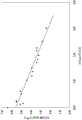
图1为在根据本发明的聚合反应方法而提供的导电聚合物涂层上进行电沉积铜中的横向铜生长速率的曲线图,该聚合反应方法是利用基于本发明的组合物的单体制剂进行的。相对于由对870nm的红外线辐射的吸收指示的单体制剂中的低聚物含量而绘制横向生长速率;和Figure 1 is a graph of the lateral copper growth rate in electrodeposited copper on a conductive polymer coating provided according to the polymerization process of the present invention using a monomer formulation based on the composition of the present invention ongoing. The lateral growth rate is plotted against the oligomer content in the monomer formulation indicated by the absorption of infrared radiation at 870 nm; and
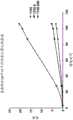
图2为低聚物形成相对于本发明的单体制剂的老化的曲线图,这通过对870nm的红外线辐射的吸收而测量。Figure 2 is a graph of oligomer formation versus aging of monomer formulations of the invention as measured by absorption of infrared radiation at 870 nm.
具体实施方式Detailed ways
根据本发明的组合物包含用于形成导电聚合物的可聚合单体(例如可聚合的杂环芳香族分子)以及上文所提到的酸。这样的单体能够与引发剂溶液中包含的氧化剂起反应,在使介电基板与本发明的组合物接触之前,用该引发剂溶液处理介电基板。例如,这样的氧化剂可为由包含高锰酸盐的引发剂溶液的沉积而得到的锰(IV)氧化物。酸催化杂环芳香族分子在介电基板(优选地为高分子树脂基板)的被氧化的表面上的聚合反应,从而在该介电基板上形成导电聚合物。该杂环芳香族分子可源自具有一个杂原子的5元芳杂环(即具有两个双键的5元环),该杂环具有以下结构:The composition according to the invention comprises a polymerizable monomer for forming a conductive polymer, such as a polymerizable heterocyclic aromatic molecule, and the above-mentioned acid. Such monomers are capable of reacting with the oxidizing agent contained in the initiator solution with which the dielectric substrate is treated prior to contacting the dielectric substrate with the composition of the invention. For example, such an oxidizing agent may be manganese(IV) oxide obtained from the deposition of an initiator solution comprising permanganate. The acid catalyzes the polymerization of heterocyclic aromatic molecules on the oxidized surface of a dielectric substrate, preferably a polymer resin substrate, thereby forming a conductive polymer on the dielectric substrate. The heterocyclic aromatic molecule can be derived from a 5-membered aromatic heterocycle with one heteroatom (i.e. a 5-membered ring with two double bonds), which has the following structure:

其中:X为O、S或N;R1和R2分别独立地为氢、卤素、具有1至8个碳原子的被取代的或未被取代的烷基、具有1至8个碳原子(例如1至4个碳原子)的被取代的或未被取代的烷氧基。该被取代的或未被取代的烷氧基可通过氧原子连接至该5元杂环。此外,R1和R2可通过具有3或4个碳原子的被取代的或未被取代的烷基或通过具有1或2个碳原子的被取代的或未被取代的烷基二氧基而一起形成5元环或6元环。该被取代的或未被取代的烷基二氧基可通过氧原子连接至5元杂环。优选地,该杂环芳香族分子可为被取代的或未被取代的噻吩(X为硫),这是因为其具有良好的传导性和加工性。优选的取代基为未被取代的乙撑二氧基,该未被取代的乙撑二氧基通过两个氧原子连接至5元噻吩环,使得该结构包括包含5元环和6元环的稠环系统。被称为3,4-乙撑二氧噻吩的物质聚合成聚(3,4-乙撑二氧噻吩),其由于极好的传导性而成为优选的导电聚合物。优选的3,4-乙撑二氧噻吩的结构为:Wherein: X is O, S or N; R1 and R2 are independently hydrogen, halogen, substituted or unsubstituted alkyl with 1 to 8 carbon atoms, 1 to 8 carbon atoms (such as 1 to 4 carbon atoms) substituted or unsubstituted alkoxy. The substituted or unsubstituted alkoxy group may be attached to the 5-membered heterocyclic ring through an oxygen atom. In addition, RandR may be substituted or unsubstituted alkyl having 3 or 4 carbon atoms or substituted or unsubstituted alkyldioxy having 1 or 2 carbon atoms And together form a 5-membered ring or a 6-membered ring. The substituted or unsubstituted alkyldioxy group may be attached to the 5-membered heterocyclic ring through an oxygen atom. Preferably, the heterocyclic aromatic molecule may be substituted or unsubstituted thiophene (X is sulfur) because of its good conductivity and processability. A preferred substituent is an unsubstituted ethylenedioxy group attached to the 5-membered thiophene ring through two oxygen atoms such that the structure includes 5-membered and 6-membered rings Fused ring system. The substance known as 3,4-ethylenedioxythiophene is polymerized into poly(3,4-ethylenedioxythiophene), which is the preferred conducting polymer due to its excellent conductivity. The structure of preferred 3,4-ethylenedioxythiophene is:
在下文中,本发明的组合物也将被称作催化剂组合物。Hereinafter, the composition of the present invention will also be referred to as catalyst composition.
作为合适的乳化剂,本发明的组合物可包括非离子型表面活性剂或阴离子型表面活性剂。尽管非离子型表面活性剂已显示出作用相当好,但阴离子型表面活性剂是优选的,这是因为添加阴离子型表面活性剂有助于降低单体制剂中的可聚合单体形成非导电低聚物。例如,合适的阴离子型乳化剂为阴离子型的多芳基酚烷氧基化物及其盐、阴离子型的芳烷基取代的磺基聚烷氧基酚(例如一苄基取代的、二苄基取代的或三苄基取代的或三-(1-苯乙基)取代的磺基聚乙氧基化的或磺基聚丙氧基化的酚)或者阴离子型的磺基烷基化的聚烷氧基化的β-萘酚(如磺基乙基化的磺基丙基化的、或磺基己基化的聚乙氧基化或聚丙基化的萘酚及其盐,如NH4+盐、Na+盐、Li+盐或异丙基铵盐)。As suitable emulsifiers, the compositions of the invention may comprise nonionic or anionic surfactants. Although nonionic surfactants have been shown to work reasonably well, anionic surfactants are preferred because the addition of anionic surfactants helps reduce the formation of non-conductive low-lying polymerizable monomers in monomer formulations. Polymer. Suitable anionic emulsifiers are, for example, anionic polyarylphenol alkoxylates and salts thereof, anionic aralkyl-substituted sulfopolyalkoxyphenols (e.g. monobenzyl substituted, dibenzyl substituted or tribenzyl substituted or tris-(1-phenylethyl) substituted sulfopolyethoxylated or sulfopolypropoxylated phenols) or anionic sulfoalkylated polyalkylenes Oxylated β-naphthols (such as sulfoethylated, sulfopropylated, or sulfohexylated polyethoxylated or polypropylated naphthols and their salts, such as NH4+ salts , Na+ salt, Li+ salt or isopropylammonium salt).
特别优选的乳化剂为Rhodia S.A.公司以名称Soprophor4D384出售的产品,该产品具有根据下列化学式的分子结构:A particularly preferred emulsifier is the product sold under the name Soprophor 4D384 by the company Rhodia S.A., which has a molecular structure according to the following chemical formula:

另一合适的乳化剂为Rhodia S.A.公司以名称Soprophor DSS/15出售的化合物,其对应于聚(氧-1,2-乙二基)α-磺基-ω-[二(1-苯乙基)苯氧基]-铵盐。Another suitable emulsifier is the compound sold under the name Soprophor DSS/15 by the company Rhodia S.A., which corresponds to poly(oxy-1,2-ethylenediyl)α-sulfo-ω-[bis(1-phenylethyl ) phenoxy]-ammonium salt.
另一特别优选的乳化剂为德国Raschig GmbH公司以名称RALUFON NAPE1490出售的产品,该产品具有根据下面化学式的分子结构:Another particularly preferred emulsifier is the product sold under the name RALUFON NAPE 1490 by the German company Raschig GmbH, which has a molecular structure according to the following chemical formula:
其具有结构:which has the structure:

通常,乳化剂可以以0.1mL/L和200mL/L之间、优选地5ml/l和100mL/L之间、更优选地10mL/L和50mL/L之间的范围包含在本发明的组合物中。Typically, emulsifiers may be included in the compositions of the invention in a range between 0.1 mL/L and 200 mL/L, preferably between 5 mL/L and 100 mL/L, more preferably between 10 mL/L and 50 mL/L middle.
本发明源自于发现催化剂组合物的组成有助于介电基板的裸露面的金属化,所述介电基板的裸露面例如为在PCB制造中通常使用的高分子树脂基板中的钻的通孔和微导孔的侧壁。尽管在下文中对本发明的描述集中于金属化钻的通孔和微导孔的侧壁,但本发明的金属化方法也普遍地适用于金属化介电基板。例如,该金属化方法可用于在制造单面层压有铜或双面层压有铜的PCB基板或层压有铜的多层基板中金属化介电基板的一面或两面。The present invention stems from the discovery that the composition of the catalyst composition facilitates the metallization of the exposed surface of a dielectric substrate, such as a drilled hole in a polymeric resin substrate commonly used in PCB manufacturing. sidewalls of holes and microvias. Although the description of the present invention hereinafter focuses on metallizing the sidewalls of drilled vias and microvias, the metallization method of the present invention is also generally applicable to metallizing dielectric substrates. For example, the metallization method can be used to metallize one or both sides of a dielectric substrate in the manufacture of single-sided copper-laminated or double-sided copper-laminated PCB substrates or copper-laminated multilayer substrates.
该催化剂组合物的特征在于,其化学成分不同于常规金属化工艺中已知的组合物且通常比常规金属化工艺中已知的组合物简单,且可用于比常规金属化工艺采用更少的步骤和更高的电流密度的金属化工艺。全部这些伴随的优点产生了有较少废液、较高的生产量、和高质量电镀的PCB产品的金属化工艺。The catalyst composition is characterized by a chemical composition that differs from and is generally simpler than compositions known in conventional metallization processes, and can be used with less step and higher current density metallization process. All of these attendant advantages result in a metallization process with less liquid waste, higher throughput, and high quality plated PCB products.
可以使用本发明的催化剂组合物的金属化工艺适用于任何介电基板材料。例如,用于印刷电路板的合适的基板材料包括纤维强化的环氧树脂基板(即,多层纤维材料在热和压力下与热固性树脂粘接在一起)。通常,环氧树脂基板包含与环氧树脂系统粘接的连续纤维玻璃布。环氧树脂基板的具体示例包括以下基板:G-10,其为包含利用玻璃纤维布薄片强化的环氧树脂的基板;FR-4,其为与G-10类似的自灭性基板;G-11,其为玻璃布和环氧树脂的混合物;和FR-5,其为G-11的耐火形式。FR-4基板可利用陶瓷颗粒强化,例如那些来自RogersCorporation(Chandler,AZ)的陶瓷颗粒。其它树脂包括聚苯醚、氰酸酯、双马来酰亚胺/三嗪。The metallization process that can use the catalyst composition of the present invention is applicable to any dielectric substrate material. For example, suitable substrate materials for printed circuit boards include fiber-reinforced epoxy substrates (ie, layers of fiber material bonded together with a thermosetting resin under heat and pressure). Typically, epoxy substrates consist of continuous fiberglass cloth bonded with an epoxy system. Specific examples of epoxy substrates include the following substrates: G-10, which is a substrate containing epoxy reinforced with a sheet of glass cloth; FR-4, which is a self-destructive substrate similar to G-10; G- 11, which is a mixture of glass cloth and epoxy resin; and FR-5, which is a fire-resistant version of G-11. FR-4 substrates can be reinforced with ceramic particles, such as those from Rogers Corporation (Chandler, AZ). Other resins include polyphenylene ethers, cyanates, bismaleimide/triazines.
可作为用于金属化的基板的另外的介电材料包括陶瓷、玻璃、特氟隆、玻璃纤维强化的特氟隆、陶瓷强化的特氟隆、聚苯乙烯和聚酰亚胺(用于柔性板应用)。Additional dielectric materials that can be used as substrates for metallization include ceramics, glass, Teflon, glass fiber reinforced Teflon, ceramic reinforced Teflon, polystyrene, and polyimide (for flexible board applications).
除了上文所述的材料外,基板还可包括例如半导体材料(如硅、SiO2或砷化镓)或无机氧化物(如氧化铝)、钛或锆。In addition to the materials described above, the substrate may also comprise, for example, semiconductor materials such as silicon,SiO2 or gallium arsenide, or inorganic oxides such as aluminum oxide, titanium or zirconium.
为了制造PCB基板,通过常规的工艺用铜箔层压在上文描述的介电基板的一面或两面上。通常使用的层压片包覆有18μm厚的铜。通过叠置高达16个铜层来形成多层电路板,其中所述16个铜层由上文描述的基板材料分离开和支撑。为了在铜层之间形成电连接,例如通过硬质合金钻头和激光钻孔,对该PCB基板钻通孔(贯穿PCB或多层电路板的整个深度的孔)和盲孔(仅沿着PCB或多层电路板的深度的一部分延伸的孔)。所钻的通孔和盲孔可使用本发明的金属化工艺进行金属化。To manufacture the PCB substrate, copper foil is laminated on one or both sides of the above-described dielectric substrate by conventional processes. A commonly used laminate is clad with 18 μm thick copper. Multilayer circuit boards are formed by stacking up to 16 copper layers separated and supported by the substrate material described above. To make electrical connections between copper layers, for example by carbide drills and laser drilling, drill through holes (holes that run through the entire depth of the PCB or multilayer circuit board) and blind holes (only along the length of the PCB) or a hole that extends for a fraction of the depth of a multilayer board). Drilled vias and blind vias can be metallized using the metallization process of the present invention.
可替代地,本发明的催化剂组合物可用在金属化工艺中以利用例如铜层层压上文描述的介电基板的全部表面,取代常规的铜层压。在利用本发明的组合物和方法进行铜沉积/电解电镀后,可对PCB基板钻通孔和盲孔,这些通孔和盲孔也可使用本发明的金属化方法进行金属化。Alternatively, the catalyst composition of the present invention may be used in a metallization process to laminate the entire surface of the dielectric substrate described above with, for example, a copper layer, instead of conventional copper lamination. After copper deposition/electroplating using the compositions and methods of the invention, through holes and blind holes can be drilled into the PCB substrate, which can also be metallized using the metallization method of the invention.
在另一替选方案中,在层压有铜的PCB基板中钻的通孔和盲孔的金属化可与铜导电图案的形成同时发生。In another alternative, the metallization of the vias and blind holes drilled in the copper laminated PCB substrate can occur simultaneously with the formation of the copper conductive pattern.
通常利用硬质合金钻头钻穿过PCB的孔。当需要极小的导孔时,可利用激光器来形成该导孔。激光器钻的导孔称作微导孔,在该孔内部的表面光洁度通常较差,这使得其金属化较难进行。这些孔被称作微导孔。该行业正在朝向直径小于150μm的微导孔发展,且该微导孔的深度可大于宽度,使得它们具有高的长宽比。Holes are usually drilled through the PCB with carbide drill bits. When extremely small vias are required, lasers can be used to form the vias. Laser-drilled vias, called microvias, typically have a poorer surface finish inside the vias, making metallization more difficult. These holes are called microvias. The industry is moving towards microvias with a diameter of less than 150 μm that can be deeper than wide, allowing them to have a high aspect ratio.
长宽比通常至少约0.5:1,在一些情况下大于约1:1。在该说明书中,长宽比为导孔深度与导孔开口的宽度的比率。还可在铜层压之前,对PCB的各个薄片进行深度受控钻孔、激光钻孔或预钻孔,以形成仅连接铜层中的一些铜层的孔,而不是穿过整个板的孔。当这些孔将内部铜层连接至外层时,这些孔被称作盲孔;或者当这些孔连接两个或更多个内部铜层时,它们被称作埋孔。The aspect ratio is generally at least about 0.5:1, and in some cases greater than about 1:1. In this specification, the aspect ratio is the ratio of the depth of the via hole to the width of the opening of the via hole. Individual slices of the PCB can also be depth-controlled drilled, laser drilled, or pre-drilled prior to copper lamination to create holes that connect only some of the copper layers, rather than through the entire board . When these holes connect an inner copper layer to an outer layer, they are called blind vias; or when they connect two or more inner copper layers, they are called buried vias.
通孔和盲孔的壁可使用本发明的金属化方法进行金属化。The walls of through holes and blind holes can be metallized using the metallization method of the present invention.
使用本发明的组合物的金属化工艺可金属化介电基板,例如通常用于PCB制造的玻璃纤维强化的环氧树脂基板。该工艺适用于对钻的通孔或微导孔镀铜,也可用于金属化介电基板以产生单面覆盖有铜或双面覆盖有铜的PCB基板。在一个实施方式中,用于使非导电基板具有导电性且进行电解镀铜的步骤包括:Metallization processes using the compositions of the present invention can metallize dielectric substrates, such as glass fiber reinforced epoxy substrates commonly used in PCB manufacturing. This process is suitable for copper plating on drilled through holes or micro vias, and can also be used to metallize dielectric substrates to produce PCB substrates covered with copper on one side or on both sides. In one embodiment, the step for making the non-conductive substrate conductive and electrolytically copper plating comprises:
1.通过将介电基板置于可使该介电基板的裸露面湿润的调节溶液中,来调节该裸露面(例如通孔或微导孔的侧壁);1. Conditioning the exposed surface of the dielectric substrate (such as the sidewall of a via or microvia) by placing the dielectric substrate in a conditioning solution that wets the exposed surface;
2.水冲洗;2. Rinse with water;
3.用包含氧化剂的组合物氧化该介电材料的在通孔和微导孔中的经调节的裸露面;3. Oxidizing the conditioned exposed surfaces of the dielectric material in the vias and microvias with a composition comprising an oxidizing agent;
4.水冲洗;4. Rinse with water;
5.利用本发明的催化剂溶液催化该被氧化的裸露面以使导电聚合物沉积在介电材料的该被氧化的裸露面上且从而使该裸露面导电,该催化剂溶液包括可聚合的杂环芳香族分子、酸、乳化剂和至少一种选自锂离子、钠离子、铝离子、铍离子、铋离子、硼离子、铟离子和/或烷基咪唑离子的金属离子;5. Utilizing the catalyst solution of the present invention to catalyze the oxidized exposed surface to deposit a conductive polymer on the oxidized exposed surface of a dielectric material and thereby make the exposed surface conductive, the catalyst solution comprising a polymerizable heterocycle Aromatic molecules, acids, emulsifiers and at least one metal ion selected from lithium ions, sodium ions, aluminum ions, beryllium ions, bismuth ions, boron ions, indium ions and/or alkylimidazolium ions;
6.水冲洗。6. Rinse with water.
然后,可通过将介电基板的表面(在该表面上具有导电聚合物)置于包括阳极和电解镀铜组合物的电解镀铜浴中且施加外部的电子源,来金属化基板。The substrate may then be metallized by placing the surface of the dielectric substrate (having the conductive polymer on the surface) in an electrolytic copper plating bath comprising an anode and an electrolytic copper plating composition and applying an external source of electrons.
在上文描述的金属化工艺中的调节溶液可包括在德国专利申请DE4205190中描述的成分,该德国专利申请的全部内容通过引用并入本文。例如,该调节溶液可包含按重量计至少0.001%的杂环芳香族分子,该杂环芳香族分子包含氮、交联剂和pH缓冲剂。包含氮的示例性芳香族分子包括吡啶、喹啉、吡咯、吲哚、吖啶、异喹啉、哒嗪、嘧啶、喹唑啉、吩嗪、噌啉、蝶啶、咔唑、吡唑、咪唑、三唑、苯并咪唑、嘌呤、异吲哚及其衍生物以及其混合物示例性的调节溶液可来自Enthone Inc.(West Haven,Conn.)且包括


将介电材料的表面置于调节溶液中,通过使表面湿润来调节表面以用于下一步骤中的氧化。在氧化之前润湿孔和导孔对于小直径的孔和导孔而言是有利的,该小直径可小于约100μm、或者甚至小于约50μm,这在钻孔的PCB基板中日益普遍。可通过任一方法使介电基板接触调节溶液,诸如淹没、浸泡或喷洒,只要该接触方法充分润湿介电基板的裸露面,诸如通孔和微导孔的侧壁。通常在约30°C至约65°C(诸如约30°C至约50°C、或者约40°C至约65°C)的温度下接触约1分钟至约6分钟(诸如约2分钟至5分钟或者约1分钟至3分钟)。The surface of the dielectric material is placed in the conditioning solution to condition the surface for oxidation in the next step by wetting the surface. Wetting the holes and vias prior to oxidation is advantageous for small diameter holes and vias, which may be less than about 100 μm, or even less than about 50 μm, which is increasingly common in drilled PCB substrates. The dielectric substrate can be exposed to the conditioning solution by any method, such as flooding, soaking, or spraying, as long as the contacting method sufficiently wets the exposed surfaces of the dielectric substrate, such as the sidewalls of vias and microvias. Usually at a temperature of about 30°C to about 65°C (such as about 30°C to about 50°C, or about 40°C to about 65°C) for about 1 minute to about 6 minutes (such as about 2 minutes) to 5 minutes or approximately 1 to 3 minutes).
在上述金属化过程中的引发剂组合物包含氧化剂。该氧化剂可选自已知类别的氧化剂,例如锰(VII)化合物、锰(VI)化合物、碘(VII)化合物、和铈(IV)化合物。上述化合物优选地为含氧化合物。例如,该氧化剂可为高锰酸盐、锰酸盐和高碘酸盐。优选的氧化剂为高锰酸盐,其可作为钠盐或钾盐提供。当高锰酸盐为引发剂溶液中的氧化剂时,接触介电基板的调节过的表面将氧化介电介质的裸露表面且产生其上沉积有锰(IV)氧化物(MnO2)膜的表面。该表面也作为氧化剂且对于随后的聚合反应是必需的。使用MnO2,形成Mn(II)离子。锰(IV)氧化物膜的密度取决于多个因素,诸如引发剂溶液中的氧化剂浓度、接触时间和接触方式。通常,引发剂溶液中的高锰酸盐浓度在约40g/L和约70g/L之间,诸如约60g/L。引发剂组合物可包含另外的湿润剂,诸如离子型含氟表面活性剂或非离子型含氟表面活性剂,以改善锰(IV)氧化物沉积。The initiator composition in the metallization process described above contains an oxidizing agent. The oxidizing agent may be selected from known classes of oxidizing agents such as manganese (VII) compounds, manganese (VI) compounds, iodine (VII) compounds, and cerium (IV) compounds. The aforementioned compounds are preferably oxygen-containing compounds. For example, the oxidizing agent may be permanganate, manganate and periodate. A preferred oxidizing agent is permanganate, which is available as a sodium or potassium salt. When permanganate is the oxidizing agent in the initiator solution, the conditioned surface in contact with the dielectric substrate will oxidize the exposed surface of the dielectric and produce a surface on which a manganese (IV) oxide (MnO2 ) film is deposited . This surface also acts as an oxidizing agent and is necessary for subsequent polymerization reactions. With MnO2 , Mn(II) ions are formed. The density of the manganese(IV) oxide film depends on several factors such as the concentration of the oxidant in the initiator solution, the contact time and the method of contact. Typically, the concentration of permanganate in the initiator solution is between about 40 g/L and about 70 g/L, such as about 60 g/L. The initiator composition may contain additional wetting agents, such as ionic or nonionic fluorosurfactants, to improve manganese(IV) oxide deposition.
当在pH为6的情况下操作时,引发剂通常包含硼酸作为缓冲剂。在生产期间磷酸用于调节pH。引发剂的成分在现有技术中是已知的且已经在例如DE4113654中公开,DE4113654通过引并入本文。When operating at pH 6, the initiator typically contains boric acid as a buffer. Phosphoric acid is used to adjust the pH during production. The composition of the initiator is known in the prior art and has been disclosed, for example, in DE4113654, which is hereby incorporated by reference.
可通过任何方法(诸如淹没、浸泡或喷洒)使高分子树脂基板的调节后的表面接触引发剂溶剂,条件是该接触方法足以在介电基板的调节后的裸露表面上生成MnO2密度介于约1mg/dm2和约10mg/dm2之间(诸如在约4mg/dm2和约6mg/dm2之间)的锰(IV)氧化物膜。接触通常在约80°C至约90°C的温度下进行约3分钟到约6分钟。示例性的引发剂溶液可来自Enthone Inc.(WestHaven,Conn.)且包括
在上述金属化工艺中的催化剂溶液可为在上文中描述的和下列实施方式中描述的本发明的组合物。The catalyst solution in the above metallization process may be the composition of the present invention described above and in the following embodiments.
可使用缓冲剂(诸如磷酸氢盐、磷酸二氢盐、醋酸盐的碱金属盐)将催化剂组合物处理至合适的pH。适于用在催化剂组合物中的溶剂包括甲醇、乙醇、正丙醇、异丙醇、高级醇、多元醇、DMF(二甲基甲酰胺)、酮(尤其是甲基乙基酮)、异丙基苯磺酸盐、N-甲基吡咯烷酮、三甘醇二甲醚、二甘醇二甲醚、甲苯磺酸盐的碱金属盐或它们的乙酯、碱性水溶液、或其混合物。The catalyst composition may be treated to a suitable pH with buffering agents such as hydrogen phosphate, dihydrogen phosphate, alkali metal salts of acetate. Solvents suitable for use in the catalyst composition include methanol, ethanol, n-propanol, isopropanol, higher alcohols, polyols, DMF (dimethylformamide), ketones (especially methyl ethyl ketone), isopropanol, Propylbenzenesulfonate, N-methylpyrrolidone, triglyme, diglyme, alkali metal salts of toluenesulfonate or their ethyl esters, alkaline aqueous solution, or a mixture thereof.
介电基板的被氧化的表面接触催化剂组合物引发被氧化的表面上的MnO2膜、可聚合的杂环芳香族分子和酸之间的反应,该反应引起聚合作用以及在介电基板的被氧化的裸露表面上沉积导电聚合物。可通过淹没、浸泡或喷洒进行该接触,且该接触通常在室温下或略微低于室温的温度下进行约1分钟和约8分钟之间,例如约2分钟和约4分钟之间。示例性的催化剂溶液可来自EnthoneInc.(West Haven,Conn.)且包括

高分子树脂基板的表面接触催化剂溶液,从而产生沉积在该表面上的导电聚合物,随后通常是冲洗步骤,该冲洗步骤之后是接触电解镀铜浴,该电解镀铜浴包含电解镀铜组合物和阳极。电解镀铜组合物包含铜离子源和酸。电解镀铜浴还可包括添加剂,诸如氯离子、抛光剂、抑制剂和晶粒细化剂,这些是现有技术中已知的。The surface of the polymeric resin substrate is contacted with a catalyst solution, thereby producing a conductive polymer deposited on the surface, followed generally by a rinsing step followed by contacting an electrolytic copper plating bath comprising an electrolytic copper plating composition and anode. An electrolytic copper plating composition comprises a source of copper ions and an acid. The electrolytic copper plating bath may also include additives such as chloride ions, polishes, inhibitors and grain refiners, which are known in the art.
铜离子源包括硫酸铜、五水合硫酸铜、氧化铜、碳酸铜、氟硼酸铜、焦磷酸铜、氰化铜、膦酸铜、和其它铜金属络合物(诸如甲基磺酸铜)。优选地,铜源为基于硫酸铜的源之一,即硫酸铜或五水合硫酸铜。铜的浓度可在宽范围内变化,例如从约5g/L铜到约75g/L Cu。在低铜系统(即电解液包含低浓度的铜)中,铜离子浓度可在约5g/L和约30g/L之间,例如约8g/L到约25g/L。示例性的低铜系统可包含8g/L的铜离子、10g/L的铜离子、20g/L的铜离子、或25g/L的铜离子。在一些高铜系统(即电解液包含高浓度的铜)中,铜离子浓度可在约35g/L和约75g/L之间,优选地在约35g/L和约60g/L之间,例如在约38g/L和约42g/L之间。在一些高铜系统中,铜离子浓度可在约46g/L和约60g/L之间,例如在约48g/L和约52g/L之间。在示例性的高铜系统中,铜离子浓度为约40g/L。Sources of copper ions include copper sulfate, copper sulfate pentahydrate, copper oxide, copper carbonate, copper fluoroborate, copper pyrophosphate, copper cyanide, copper phosphonate, and other copper metal complexes such as copper methanesulfonate. Preferably, the copper source is one of the copper sulfate based sources, namely copper sulfate or copper sulfate pentahydrate. The concentration of copper can vary over a wide range, for example from about 5 g/L copper to about 75 g/L Cu. In a low copper system (ie, the electrolyte contains a low concentration of copper), the copper ion concentration may be between about 5 g/L and about 30 g/L, such as about 8 g/L to about 25 g/L. Exemplary low copper systems may include 8 g/L copper ions, 10 g/L copper ions, 20 g/L copper ions, or 25 g/L copper ions. In some high copper systems (i.e. the electrolyte contains a high concentration of copper), the copper ion concentration may be between about 35 g/L and about 75 g/L, preferably between about 35 g/L and about 60 g/L, for example between about Between 38g/L and about 42g/L. In some high copper systems, the copper ion concentration may be between about 46 g/L and about 60 g/L, such as between about 48 g/L and about 52 g/L. In an exemplary high copper system, the copper ion concentration is about 40 g/L.
在另一示例性的高铜系统中,铜离子浓度为约50g/L。在又一示例性的高铜系统中,铜离子浓度为约75g/L。为了达到约5g/L的铜浓度,每1L溶液添加约19克的五水合硫酸铜。为了达到约75g/L的铜浓度,每1L溶液添加约292克的五水合硫酸铜。In another exemplary high copper system, the copper ion concentration is about 50 g/L. In yet another exemplary high copper system, the copper ion concentration is about 75 g/L. To achieve a copper concentration of about 5 g/L, about 19 grams of copper sulfate pentahydrate were added per 1 L of solution. To achieve a copper concentration of about 75 g/L, about 292 grams of copper sulfate pentahydrate were added per 1 L of solution.
氯离子也可以以高达200mg/L的浓度用在电解电镀浴中,例如以在约40mg/L和约200mg/L之间的浓度、或约10mg/L到90mg/L的浓度用在电解电镀浴中。在这些浓度范围内添加氯离子以增强浴中的其它添加剂的功能。典型的氯离子源包括盐酸和氯化物的碱金属盐,更常见地为氯化钠。可添加现有技术中已知的其它添加剂,如抛光剂、抑制剂和晶粒细化剂。优选的电解镀铜添加剂为来自Enthone Inc.(West Haven,Conn.)的LP-1添加剂,其可以以约2mL/L和约8mL/L之间的浓度、更优选地以约3mL/L和约6mL/L之间的浓度(诸如以约4mL/L或约5mL/L的浓度)添加。在电镀浴中的酸源包括硫酸、甲烷磺酸、磷酸和某些高分子酸(诸如聚苯乙烯磺酸)。通常,在常规的铜电镀组合物中,酸可以以约50g/L和约300g/L之间的浓度、更普遍地以约100g/L和约220g/L之间的浓度(诸如约200g/L的浓度)存在。Chloride ions may also be used in the electrolytic plating bath at a concentration of up to 200 mg/L, for example at a concentration between about 40 mg/L and about 200 mg/L, or at a concentration of about 10 mg/L to 90 mg/L middle. Chloride ions are added within these concentration ranges to enhance the function of other additives in the bath. Typical sources of chloride ions include hydrochloric acid and alkali metal salts of chloride, more commonly sodium chloride. Other additives known in the art, such as polishing agents, inhibitors and grain refiners, may be added. A preferred electrolytic copper plating additive is ® from Enthone Inc. (West Haven, Conn.) LP-1 additive, which may be present at a concentration between about 2mL/L and about 8mL/L, more preferably at a concentration between about 3mL/L and about 6mL/L (such as at about 4mL/L or about 5mL/L concentration) added. Acid sources in electroplating baths include sulfuric acid, methanesulfonic acid, phosphoric acid, and certain polymeric acids such as polystyrenesulfonic acid. Typically, in conventional copper electroplating compositions, the acid may be present at a concentration between about 50 g/L and about 300 g/L, more commonly between about 100 g/L and about 220 g/L (such as about 200 g/L concentration) exists.
在本发明的优选实施方式中,酸在催化剂组合物中保持低浓度,诸如在约0.1g/L和约30g/L之间、更优选地在约1g/L和约3g/L之间的浓度,以达到溶液pH值在约1和约3.5之间,优选地在约1.5和约3.5之间,更优选地在约1.5和约2.5之间,诸如约2。例如,可以以约1g/L的浓度添加硫酸以实现溶液pH约2。可替选地,在一个优选的实施方式中,可以以约2.5g/L的浓度添加高分子酸(诸如聚苯乙烯磺酸)以实现溶液pH约2。根据本发明,为了实现pH介于约1.5和2.5之间,采用约1g/L(例如在约0.5g/L和约10g/L之间,或在约0.5g/L和约5g/L之间)的酸添加剂。这与常规的酸铜浴相反,常规的酸铜浴采用至少50g/L的酸,例如约200g/L的硫酸。常规浴的pH通常不被测量或者是不可测量的,因此酸度表征为g/L的酸。本发明的该方面适于在导电基板上的常规电镀以及在利用导电聚合物处理的介电基板上的电镀。In a preferred embodiment of the invention, the acid is kept at a low concentration in the catalyst composition, such as a concentration between about 0.1 g/L and about 30 g/L, more preferably between about 1 g/L and about 3 g/L, to achieve a solution pH of between about 1 and about 3.5, preferably between about 1.5 and about 3.5, more preferably between about 1.5 and about 2.5, such as about 2. For example, sulfuric acid can be added at a concentration of about 1 g/L to achieve a solution pH of about 2. Alternatively, in a preferred embodiment, a polymeric acid such as polystyrene sulfonic acid may be added at a concentration of about 2.5 g/L to achieve a solution pH of about 2. According to the present invention, to achieve a pH between about 1.5 and 2.5, about 1 g/L is used (eg, between about 0.5 g/L and about 10 g/L, or between about 0.5 g/L and about 5 g/L) acid additives. This is in contrast to conventional acid copper baths, which employ at least 50 g/L of acid, such as about 200 g/L of sulfuric acid. The pH of conventional baths is usually not measured or is not measurable, so acidity is characterized as g/L acid. This aspect of the invention is suitable for conventional electroplating on conductive substrates as well as electroplating on dielectric substrates treated with conductive polymers.
在本发明的催化剂组合物的另一实施方式中,催化剂组合物另外地包含铜离子源,且将在接触催化剂溶液后发生的冲洗步骤去除。在该实施方式中,催化剂组合物的成分和电解镀铜组合物的成分混合形成单一组合物。该组合物能够在介电基板的裸露表面上沉积导电聚合物以及利用所施加的电流将铜沉积在导电聚合物的表面上。使用普通的铜浴是不可能实现这一点的,因为普通铜浴的酸浓度高且会发生单体(EDT)沉降。In another embodiment of the catalyst composition according to the invention, the catalyst composition additionally comprises a source of copper ions and the washing step which occurs after contacting the catalyst solution is removed. In this embodiment, the components of the catalyst composition and the components of the electrolytic copper plating composition are mixed to form a single composition. The composition is capable of depositing a conductive polymer on a bare surface of a dielectric substrate and depositing copper on the surface of the conductive polymer with an applied electric current. This is not possible with common copper baths due to their high acid concentration and monomer (EDT) settling.
示例性的催化剂组合物/电解镀铜组合物包含可聚合的杂环芳香族分子、铜离子源、酸和其它通常添加到电解镀铜组合物中的添加剂。催化剂组合物/电解镀铜组合物的成分的特性和浓度基本上与上文结合单独的溶液描述的成分的特性和浓度相同。An exemplary catalyst composition/electrolytic copper plating composition comprises a polymerizable heterocyclic aromatic molecule, a source of copper ions, an acid, and other additives commonly added to electrolytic copper plating compositions. The identity and concentration of the ingredients of the catalyst composition/electrolytic copper plating composition are substantially the same as those described above in connection with the individual solutions.
该组合的溶液和组合的操作的优点是去除中间的冲洗步骤、不再需要单独的催化容器和电解电镀容器以及整体处理时间减少。The advantages of this combined solution and combined operation are elimination of intermediate rinse steps, no need for separate catalytic and electrolytic plating vessels, and overall process time reduction.
在使用本发明的催化剂组合物执行该工艺期间,上文描述的组合物用于将铜沉积在单面层压有铜或双面层压有铜的PCB基板或多层电路板基板的通孔和微导孔的侧壁上。在一个实施方式中,将铜镀到通孔和微导孔的侧壁上的工艺包括以下步骤:The composition described above is used for depositing copper in through-holes of PCB substrates or multilayer circuit board substrates laminated with copper on one side or laminated on both sides of copper during the execution of the process using the catalyst composition of the present invention and on the sidewalls of the microvias. In one embodiment, the process of plating copper onto the sidewalls of the vias and microvias includes the steps of:
1.在单面层压有铜或双面层压有铜的PCB基板或多层电路板基板中,使用硬质合金钻头钻通孔,或使用激光钻孔钻微导孔;1. In the PCB substrate or multi-layer circuit board substrate with copper laminated on one side or double-sided laminated copper, use cemented carbide drills to drill through holes, or use laser drilling to drill micro-guide holes;
2.通过在40°C下使该基板接触
3.水冲洗;3. Rinse with water;
4.通过在80°C下使该基板接触
5.水冲洗;5. Rinse with water;
6.通过使该基板接触包含以下物质的组合物来在通孔壁或微导孔壁的被氧化的表面上沉积导电聚合物:
7.水冲洗;7. Rinse with water;
8.通过以下步骤在通孔壁或微通孔壁的表面上的导电聚合物上电解电镀铜:8. Electrolytic electroplating of copper on the conductive polymer on the surface of the via wall or microvia wall by the following steps:
(a)将基板置于包含阳极和电解镀铜组合物的电解电镀浴中,该电解镀铜组合物包含五水合硫酸铜(80g/L)、硫酸(1g/L以达到pH为2)、氯离子(60mg/L)和
(b)向基板施加电流(3A,5分钟)以将铜沉积在通孔壁和微导孔壁上。(b) Current (3 A, 5 min) was applied to the substrate to deposit copper on the walls of the vias and microvias.
使用上文所述的方法,可在PCB或多层电路板基板中的通孔壁和微导孔壁上镀高质量的沉积铜。上文所述的工艺也可用于在未预先涂覆铜箔的裸介电基板(即,玻璃纤维强化的环氧树脂基板)上镀铜层压片。另外,上文所述的工艺还可用于在预先钻有通孔的裸介电基板(即,玻璃纤维强化的环氧树脂基板)的一面或两面上镀铜层压片以及在通孔和微导孔的侧壁上镀铜。Using the methods described above, high-quality deposited copper can be plated on the walls of vias and microvias in PCB or multilayer circuit board substrates. The process described above can also be used to plate copper laminates on bare dielectric substrates (ie, glass fiber reinforced epoxy substrates) that have not been pre-coated with copper foil. Alternatively, the process described above can be used to plate copper laminates on one or both sides of a bare dielectric substrate (i.e., glass fiber reinforced epoxy substrate) The sidewalls of the vias are plated with copper.
在另一实施方式中,将铜镀在通孔和微导孔的侧壁上的工艺包括以下步骤:In another embodiment, the process of plating copper on the sidewalls of the vias and microvias includes the steps of:
1.在单面层压有铜或双面层压有铜的PCB基板或多层电路板基板中,使用硬质合金钻头钻通孔,或使用激光钻孔钻微导孔;1. In the PCB substrate or multi-layer circuit board substrate with copper laminated on one side or double-sided laminated copper, use cemented carbide drills to drill through holes, or use laser drilling to drill micro-guide holes;
2.通过在40°C下使该基板接触
3.水冲洗;3. Rinse with water;
4.通过在80°C下使该基板接触
5.水冲洗;5. Rinse with water;
6.通过使基板接触催化剂溶液/电解电镀组合物3分钟,来使导电聚合物沉积在通孔壁或微导孔壁的被氧化的表面上,该催化剂溶液/电解电镀组合物包括HDI催化剂7350A(15mL/L,包含3,4-乙撑二氧噻吩和乳化剂)和HDI催化剂7350B(15mL/L,包含聚苯乙烯磺酸)、至少一种选自锂离子、钠离子、铝离子、铍离子、铋离子、硼离子、铟离子和烷基咪唑离子的金属离子或含氮离子、五水合硫酸铜(80g/L)、硫酸(1g/L以达到pH为2)、氯离子(60mg/L)和
7.通过向基板施加电流(1A/dm2到2A/dm2,5分钟),利用电解方式将铜镀在其上具有导电聚合物的通孔壁或微导孔壁的表面上,以将铜沉积在通孔壁和微导孔上。7. By applying a current (1A/dm2 to 2A/dm2 , 5 minutes) to the substrate, copper is electrolytically plated on the surface of the via wall or microvia wall with a conductive polymer on it to Copper is deposited on the via walls and microvias.
使用上述方法,可将高质量的铜沉积在PCB或多层基板中的通孔壁和微导孔壁上。Using the methods described above, high-quality copper can be deposited on the walls of vias and microvias in PCBs or multilayer substrates.
在另一实施方式中,使用本发明的催化剂组合物的工艺可用于将铜镀在PCB或多层基板的通孔和微导孔的壁上,该PCB或多层基板进一步被处理以产生铜导电图案。在该工艺中的步骤为:In another embodiment, the process using the catalyst composition of the present invention can be used to plate copper on the walls of vias and microvias in PCBs or multilayer substrates that are further processed to produce copper conductive pattern. The steps in this process are:
1.对通过常规工艺或通过上文所述工艺中的一种工艺而在一面或两面上层压铜的玻璃纤维强化的环氧树脂基板钻孔;1. Drilling holes in fiberglass reinforced epoxy substrates laminated with copper on one or both sides by conventional processes or by one of the processes described above;
2.利用调节剂、引发剂和本发明的催化剂组合物处理钻有孔的板以将导电聚合物膜沉积在所钻的通孔的侧壁上;2. Treating the drilled plate with a modifier, an initiator and a catalyst composition of the present invention to deposit a conductive polymer film on the sidewalls of the drilled through-holes;
3.将光致抗蚀剂涂在铜箔上;3. Apply photoresist on the copper foil;
4.应用图案掩模,其中铜导电图案是暗的而掩模的其它部分为透明的;4. Apply a pattern mask where the copper conductive pattern is dark and the rest of the mask is transparent;
5.利用紫外光辐射掩模,使得光区域下面的光致抗蚀剂材料可溶,该光区域确定铜导电图案;5. Using UV light to irradiate the mask so that the photoresist material under the photoresist area that defines the copper conductive pattern is soluble;
6.去除图案掩模;6. Remove the pattern mask;
7.应用碱性显影剂,该碱性显影剂使未被辐射的光致抗蚀剂(在显影剂中可溶,显影剂通常包含碳酸钠)溶解。在该情况下,形成负像,即所谓的添加剂技术。在将形成铜轨道的位置去除光致抗蚀剂。在随后电镀中,将铜沉积在被辐射的抗蚀剂之间的“凹槽”中以及沉积在通孔或微导孔中;7. Application of an alkaline developer that dissolves the non-irradiated photoresist (soluble in the developer, which typically contains sodium carbonate). In this case, a negative image is formed, the so-called additive technique. Remove the photoresist where the copper tracks will be formed. Copper is deposited in the "grooves" between the irradiated resists and in vias or microvias during subsequent electroplating;
8.使用pH为2的电解镀铜浴,利用电解方式在裸露图案上镀约5微米厚度的铜(也对通孔进行电镀)。为了随后镀至25微米(正常厚度),可使用具有高酸含量(从约200g/L到约250g/L)的铜浴;8. Using an electrolytic copper plating bath with a pH of 2, electrolytically plate the exposed pattern with copper to a thickness of approximately 5 microns (thru holes are also plated). For subsequent plating down to 25 microns (normal thickness), copper baths with high acid content (from about 200 g/L to about 250 g/L) can be used;
9.利用锡-铅或其它抗蚀剂材料保护铜导体图案,该锡-铅或其它抗蚀剂材料防止氧化且作为抗蚀图案;9. Protecting the copper conductor pattern with tin-lead or other resist material which prevents oxidation and acts as a resist pattern;
10.利用溶剂(通常为市场上可买到的强碱性溶液)溶解剩余的光致抗蚀剂;10. Use a solvent (usually a strong alkaline solution available on the market) to dissolve the remaining photoresist;
11.利用酸溶解铜箔,从而裸露出树脂基板。由于铜导电图案受抗蚀剂保护,故不溶解;11. Use acid to dissolve the copper foil to expose the resin substrate. Since the copper conductive pattern is protected by the resist, it does not dissolve;
12.除去金属抗蚀剂。12. Remove metal resist.
因此,使用本发明的催化剂组合物的工艺可用于选择性地金属化包铜介电基板的裸露表面,例如已经穿过介电基板所钻的通孔的侧壁,以在环氧玻璃纤维基板的一面上的铜层压片与在环氧玻璃纤维基板的另一面上的铜层压片之间建立电连接。该工艺还可用于金属化介电基板的整个表面。Thus, processes using the catalyst compositions of the present invention can be used to selectively metallize exposed surfaces of copper-clad dielectric substrates, such as the sidewalls of vias that have been drilled through the dielectric An electrical connection is established between the copper laminate on one side of the substrate and the copper laminate on the other side of the epoxy fiberglass substrate. This process can also be used to metallize the entire surface of a dielectric substrate.
在另一方面中,本发明涉及介电基板上的导电聚合物层,其特征在于,所述聚合物层包括金属离子、或选自锂离子、钠离子、铝离子、铍离子、铋离子、硼离子、铟离子和烷基咪唑离子的其它金属的或含氮的离子。令人惊奇地发现,当使用如上文所述的用于在介电基板的表面上形成导电聚合物的组合物时,包含在该组合物中的金属离子或含氮离子并入到该导电聚合物层中。尽管不受缚于该理论,但是认为金属离子并入到导电聚合物层中有助于导电聚合物层的传导性,从而减小导电聚合物层的电阻。In another aspect, the invention relates to a conductive polymer layer on a dielectric substrate, characterized in that said polymer layer comprises metal ions, or is selected from lithium ions, sodium ions, aluminum ions, beryllium ions, bismuth ions, Boron ions, indium ions and other metallic or nitrogen-containing ions of alkylimidazolium ions. It has surprisingly been found that when using a composition as described above for forming a conductive polymer on the surface of a dielectric substrate, metal ions or nitrogen-containing ions contained in the composition are incorporated into the conductive polymer in the material layer. While not being bound by this theory, it is believed that the incorporation of metal ions into the conductive polymer layer contributes to the conductivity of the conductive polymer layer, thereby reducing the electrical resistance of the conductive polymer layer.
选自锂离子、钠离子、铝离子、铍离子、铋离子、硼离子、铟离子和烷基咪唑离子的金属离子或含氮离子可以以至少0.01%、优选地至少0.05%、更优选地至少0.1%的原子浓度包含在导电聚合物层中。Metal ions or nitrogen-containing ions selected from lithium ions, sodium ions, aluminum ions, beryllium ions, bismuth ions, boron ions, indium ions and alkylimidazolium ions may be present in at least 0.01%, preferably at least 0.05%, more preferably at least An atomic concentration of 0.1% is contained in the conductive polymer layer.
这些离子到金属表面的并入可通过适合的分析方法来进行测量,如ESCA(化学分析电子光谱法)、GDOES(辉光放电光发射谱仪)、或AES(俄歇电子能谱学)。The incorporation of these ions to the metal surface can be measured by suitable analytical methods, such as ESCA (electron spectroscopy for chemical analysis), GDOES (glow discharge optical emission spectroscopy), or AES (Auger electron spectroscopy).
下列实施例进一步说明本发明。The following examples further illustrate the invention.
图1为示出横向铜生长与单体制剂(催化剂溶液)中的非导电低聚物的浓度的相关性的推演图,介电基板与单体制剂接触以形成导电聚合物涂层,在该导电聚合物涂层上以电解方式沉积铜。Figure 1 is a derived graph showing the dependence of lateral copper growth on the concentration of non-conductive oligomers in a monomer formulation (catalyst solution) with which a dielectric substrate is contacted to form a conductive polymer coating, in which Copper is deposited electrolytically on the conductive polymer coating.
图1示出基板表面上的横向铜生长(LCGR)对催化剂组合物中的非导电低聚物的浓度的相关性,该催化剂组合物用于将导电聚合物膜沉积在该基板表面上。从图1可得知,根据本领域已知的常规方法(如ENVISION HDI方法)处理以沉积导电聚合物膜的标准试样(层压材料IS410,带大小为10cm×3cm,无铜区域7cm×3cm)上的LCGR随着催化剂组合物中的单体化合物的低聚物的浓度增大而减小,其中由该单体化合物形成聚合物。在沉积导电聚合物膜后,在市场出售的来自ENTHONE Inc.的名称为LP-1的铜电解液中,在电流密度2A/dm2下对试样进行镀铜5分钟。通过紫外线-可见光(UV-VIS)光谱中的870nm处的吸收,来测量催化剂组合物中的低聚物的相对浓度。当新鲜的催化剂组合物在870nm处的吸收为约零时,LCGR为大约5.5mm/分钟,但当由非导电低聚物引起的吸收增大至约3.0时,LCGR降低至约2.5mm/分钟。这提供了催化剂组合物中的非导电低聚物对于随后的金属电镀过程起到的作用。Figure 1 shows the dependence of lateral copper growth (LCGR) on a substrate surface on the concentration of non-conductive oligomers in a catalyst composition used to deposit a conductive polymer film on the substrate surface. As can be seen from Figure 1, a standard sample (laminate IS410 with a strip size of 10 cm x 3 cm and a copper-free area of 7 cm x 3 cm) decreases with increasing concentration of oligomers of monomeric compounds in the catalyst composition from which polymers are formed. After deposition of the conductive polymer film, the samples were copper-plated at a current density of 2 A/dm2 for 5 minutes in a commercially available copper electrolyte from ENTHONE Inc. under the designation LP-1. The relative concentration of oligomers in the catalyst composition was measured by absorption at 870 nm in the ultraviolet-visible (UV-VIS) spectrum. When the absorption at 870nm of the fresh catalyst composition is about zero, the LCGR is about 5.5 mm/min, but when the absorption due to the non-conductive oligomer increases to about 3.0, the LCGR decreases to about 2.5 mm/min . This provides insight into the role played by the non-conductive oligomers in the catalyst composition for the subsequent metal plating process.
实施例1Example 1
实施例1用作比较例且代表根据现有技术的催化剂组合物。将500mL的去离子水置于1000mL的烧杯中。边搅拌边加入45mL的

实施例2Example 2
将500mL的去离子水置于1000mL的烧杯中。边搅拌边加入45mL的

实施例3Example 3
将500mL的去离子水置于1000mL的烧杯中。边搅拌边加入45mL的HDI催化剂7350B(包含聚苯乙烯磺酸)和15mL的HDI催化剂7350A(包含3,4-乙撑二氧噻吩和乳化剂)。将3.8g的Al2(SO4)3*16H2O添加到该混合物中。通过440mL去离子水将混合物装满至体积1000mL。在25.8°C下,该混合物的pH值为2.21。在表1中列出了在几天的使用期后,催化剂组合物在UV-VIS光谱中870nm处的吸收值。Place 500 mL of deionized water in a 1000 mL beaker. While stirring, add 45mL of HDI Catalyst 7350B (contains polystyrenesulfonic acid) and 15mL of HDI catalyst 7350A (contains 3,4-ethylenedioxythiophene and emulsifier). 3.8 g of Al2 (SO4 )3 *16H2 O were added to the mixture. The mixture was brought to a volume of 1000 mL by 440 mL of deionized water. At 25.8°C, the pH of this mixture is 2.21. In Table 1 are listed the absorbance values at 870 nm of the catalyst compositions in the UV-VIS spectrum after a service period of several days.
实施例4Example 4
将500mL的去离子水置于1000mL的烧杯中。边搅拌边加入45mL的
实施例5Example 5
将500mL的去离子水置于1000mL的烧杯中。边搅拌边加入45mL的
实施例6Example 6
将500mL的去离子水置于1000mL的烧杯中。边搅拌边加入46mL的

实施例7Example 7
将500mL的去离子水置于1000mL的烧杯中。边搅拌边加入46mL的平均分子量约75kDa的聚苯乙烯磺酸(市场上由AkzoNobel AB出售的名称为VersaTL77)和15.5mL的HDI催化剂7350A(包含3,4-乙撑二氧噻吩和乳化剂)。将2.5g的BeSO4*4H2O添加到该混合物中。通过440mL去离子水使混合物的体积达1002mL。在22.2°C下,该混合物的pH值为3.46。通过添加26滴硫酸(50%)使22.3°C下的pH值为1.97。在表1中列出了在几天的使用期后,催化剂组合物在UV-VIS光谱中870nm处的吸收值。Place 500 mL of deionized water in a 1000 mL beaker. Add 46 mL of polystyrene sulfonic acid (commercially sold by AkzoNobel AB under the name of VersaTL77) with an average molecular weight of about 75 kDa and 15.5 mL of HDI catalyst 7350A (contains 3,4-ethylenedioxythiophene and emulsifier). 2.5 g of BeSO4 *4H2 O were added to the mixture. The volume of the mixture was brought to 1002 mL by 440 mL of deionized water. At 22.2°C, the pH of this mixture is 3.46. The pH was brought to 1.97 at 22.3°C by adding 26 drops of sulfuric acid (50%). In Table 1 are listed the absorbance values at 870 nm of the catalyst compositions in the UV-VIS spectrum after a service period of several days.
实施例8Example 8
将500mL的去离子水置于1000mL的烧杯中。边搅拌边加入45mL的平均分子量约1000kDa的聚苯乙烯磺酸(市场上由AkzoNobel AB出售的名称为Versa TL501)和15.5mL的
实施例9Example 9
将500mL的去离子水置于1000mL的烧杯中。边搅拌边加入23mL的平均分子量约1000kDa的聚苯乙烯磺酸(市场上由AkzoNobel AB出售的名称为VersaTL501)、23mL的平均分子量约75kDa的聚(4-苯乙烯磺酸)锂盐溶液(水中的重量百分比为30%)和15mL的
实施例10Example 10
将500mL的去离子水置于1000mL的烧杯中。边搅拌边加入23mL的平均分子量约1000kDa的聚苯乙烯磺酸(市场上由AkzoNobel AB出售的名称为VersaTL501)、23mL的平均分子量为75kDa的聚(4-苯乙烯磺酸)钠盐溶液(水中的重量百分比为30%,市场上由AkzoNobel AB出售的名称为Versa TL77)和15mL的
实施例11Example 11
将500mL的去离子水置于1000mL的烧杯中。边搅拌边加入46mL的HDI催化剂7350B(包含聚苯乙烯磺酸)和15mL的包含重量百分比为10%的3,4-乙撑二氧噻吩和作为乳化剂的重量百分比为12%的Soprophor4D384的水溶液。通过440mL去离子水使混合物的体积达1001mL。21.2°C下该混合物的pH值为2.13。在表1中列出了在几天的使用期后,催化剂组合物在UV-VIS光谱中870nm处的吸收值。Place 500 mL of deionized water in a 1000 mL beaker. While stirring, add 46mL of HDI catalyst 7350B (containing polystyrene sulfonic acid) and 15 mL of an aqueous solution containing 10% by weight of 3,4-ethylenedioxythiophene and 12% by weight of Soprophor 4D384 as an emulsifier. The volume of the mixture was brought to 1001 mL by 440 mL of deionized water. The pH of the mixture was 2.13 at 21.2°C. In Table 1 are listed the absorbance values at 870 nm of the catalyst compositions in the UV-VIS spectrum after a service period of several days.
实施例12Example 12
将500mL的去离子水置于1000mL的烧杯中。边搅拌边加入45mL的HDI催化剂7350B(包含聚苯乙烯磺酸)和15mL的包含重量百分比为10%的3,4-乙撑二氧噻吩和作为乳化剂的重量百分比为6%的Soprophor4D384和重量百分比为6%的Soprophor TS29的水溶液。20.6°C下该混合物的pH值为1.97。在表1中列出了在几天的使用期后,催化剂组合物在UV-VIS光谱中870nm处的吸收值。Place 500 mL of deionized water in a 1000 mL beaker. While stirring, add 45mL of HDI Catalyst 7350B (containing polystyrene sulfonic acid) and 15 mL of 3,4-ethylenedioxythiophene containing 10% by weight and Soprophor 4D384 at 6% by weight as emulsifier and Soprophor 4D384 at 6% by weight Aqueous solution of TS29. The pH of the mixture was 1.97 at 20.6°C. In Table 1 are listed the absorbance values at 870 nm of the catalyst compositions in the UV-VIS spectrum after a service period of several days.
实施例13Example 13
将500mL的去离子水置于1000mL的烧杯中。加入45mL的1:1比例的平均分子量约25kDa的聚苯乙烯磺酸(市场上由AkzoNobel AB出售的名称为VersaTL4)和马来酸的混合物以及15mL的
表1:催化剂溶液在870nm处的吸收Table 1: Absorption of Catalyst Solutions at 870nm

实施例14Example 14
将500mL去离子水加入1000mL烧杯中。然后,边搅拌边将15mL组合物A(包含3,4-乙撑二氧噻吩(3,4-EDT)和Soprophor TS29)和46mL组合物B(包含分子量为75,000Da的聚苯乙烯磺酸和水)加入到烧杯内的水中,该组合物B以商品名称Versa TL71出售。持续搅拌直到观察到完全溶解。Add 500 mL of deionized water to a 1000 mL beaker. Then, 15 mL of composition A (containing 3,4-ethylenedioxythiophene (3,4-EDT) and Soprophor TS29) and 46 mL of composition B (containing polystyrenesulfonic acid with a molecular weight of 75,000 Da and water) was added to the water in the beaker, this composition B was sold under the trade name Versa TL71. Stirring was continued until complete dissolution was observed.
实施例15Example 15
将500mL去离子水加入1000mL烧杯中。然后,边搅拌边将1-乙基-3-甲基咪唑三氟甲磺酸盐(EMI三氟甲磺酸盐;10g)、15mL组合物A(包含3,4-乙撑二氧噻吩(3,4-EDT)和Soprophor TS29)和45mL组合物B(包含分子量为75,000Da的聚苯乙烯磺酸和水)、以及440mL去离子水加入到烧杯内的水中,该组合物B以商品名称Versa TL71出售。持续搅拌直到观察到完全溶解。Add 500 mL of deionized water to a 1000 mL beaker. Then, 1-ethyl-3-methylimidazolium triflate (EMI triflate; 10 g), 15 mL of composition A (containing 3,4-ethylenedioxythiophene ( 3,4-EDT) and Soprophor TS29) and 45 mL of composition B (comprising polystyrene sulfonic acid with a molecular weight of 75,000 Da and water), and 440 mL of deionized water were added to the water in the beaker. Versa TL71 for sale. Stirring was continued until complete dissolution was observed.
实施例16Example 16
将500mL去离子水加入1000mL烧杯中。然后,边搅拌边将1-己基-3-甲基咪唑(HMI)(三氟甲基磺酰)酰亚胺(9.9g)、16mL组合物A(包含3,4-乙撑二氧噻吩(3,4-EDT)和Soprophor TS29)和46mL组合物B(包含分子量为75,000Da的聚苯乙烯磺酸和水)、以及440mL去离子水加入到烧杯内的水中,该组合物B以商品名称Versa TL71出售。持续搅拌直到观察到完全溶解。溶液保持浑浊的乳白色。Add 500 mL of deionized water to a 1000 mL beaker. Then, 1-hexyl-3-methylimidazole (HMI) (trifluoromethylsulfonyl)imide (9.9 g), 16 mL of composition A (containing 3,4-ethylenedioxythiophene ( 3,4-EDT) and Soprophor TS29) and 46 mL of composition B (comprising polystyrene sulfonic acid with a molecular weight of 75,000 Da and water), and 440 mL of deionized water were added to the water in the beaker. Versa TL71 for sale. Stirring was continued until complete dissolution was observed. The solution remained cloudy milky white.
实施例17Example 17
将500mL去离子水加入1000mL烧杯中。然后,边搅拌边将硫酸锂(2g)、一水合硫酸锰(2g)、15mL组合物A(包含3,4-乙撑二氧噻吩(3,4-EDT)和Soprophor TS29)和46mL组合物B(包含分子量为75,000Da的聚苯乙烯磺酸和水)、以及440mL去离子水加入到烧杯内的水中,该组合物B以商品名称VersaTL71出售。持续搅拌直到观察到完全溶解。.Add 500 mL of deionized water to a 1000 mL beaker. Then, lithium sulfate (2 g), manganese sulfate monohydrate (2 g), 15 mL of composition A (containing 3,4-ethylenedioxythiophene (3,4-EDT) and Soprophor TS29) and 46 mL of composition Composition B (comprising polystyrene sulfonic acid with a molecular weight of 75,000 Da and water), and 440 mL of deionized water were added to the water in the beaker, this composition B was sold under the trade name VersaTL71. Stirring was continued until complete dissolution was observed. .
低聚物的测量Measurement of oligomers
根据实施例14、实施例15和实施例17制备的各种催化剂溶液在制备后2天、27天、86天、99天和105天时,进行870nm的UV-IS吸收分析。在下面表2中列出结果:Various catalyst solutions prepared according to Example 14, Example 15 and Example 17 were subjected to UV-IS absorption analysis at 870 nm at 2 days, 27 days, 86 days, 99 days and 105 days after preparation. The results are listed in Table 2 below:
表2Table 2
*以1:10稀释即1mL催化剂溶液和9mL去离子水进行的测量。*Measurements made at a 1:10 dilution i.e. 1 mL of catalyst solution and 9 mL of deionized water.
在图2中绘制表2中的数据。根据这些数据,对于实施例14、实施例15和实施例17分别计算吸收相对于时间的增长速率。表3给出吸收的连续测量之间的吸收增长速率(斜率)。The data in Table 2 are plotted in Figure 2. From these data, the rate of increase in absorption versus time was calculated for Example 14, Example 15, and Example 17, respectively. Table 3 gives the absorption growth rate (slope) between successive measurements of absorption.
表3table 3
可应用线性回归分析来计算低聚物形成趋势线,其产生下列的斜率和相关系数:Linear regression analysis can be applied to calculate oligomer formation trendlines, which yield the following slopes and correlation coefficients:
表4Table 4
在实施例14和实施例17的情况下,计算结果示出良好的一致性。仅在实施例15的情况下,存在明显偏差。在后者情况下,在初期,斜率不是线性的,但从吸光度达到0.2时,斜率较大。对于其它两个系统,斜率始终是基本上线性的,使得相关系数非常接近1.0。In the case of Example 14 and Example 17, the calculation results showed good agreement. Only in the case of Example 15 is there a significant deviation. In the latter case, the slope is not linear initially, but becomes steeper from absorbance to 0.2. For the other two systems, the slope is consistently substantially linear, making the correlation coefficient very close to 1.0.
105天后的沉积速率Sedimentation rate after 105 days
在105天后,实施例14到实施例17的单体制剂分别用于在介电基板上提供导电聚合物层。After 105 days, the monomer formulations of Examples 14 to 17 were each used to provide a conductive polymer layer on a dielectric substrate.
在正面和背面上,用刻度尺测量每一面的边缘处和中间处的在电解电镀步骤中所沉积的铜的厚度且以mm计。将每一面的三个值相加并除以12。也对这两个均值求和然后再次除以2。因此,每分钟沉积速率以mm/分钟表示。On the front and back sides, the thickness of the copper deposited in the electrolytic plating step at the edges and in the middle of each side was measured in mm with a scale. Add the three values for each side and divide by 12. Also sum the two means and divide by 2 again. Therefore, the deposition rate per minute is expressed in mm/minute.
在聚合反应期间,对于实施例14到实施例17中的每一实施例,以毫米每分钟确定平均沉积速率。在下表4中列出了在单体制剂(催化剂溶液)已经经过105天后而进行的聚合物反应的结果。During the polymerization reaction, for each of Examples 14 through 17, the average deposition rate was determined in millimeters per minute. In Table 4 below are listed the results of the polymerisation reactions performed after the monomer formulation (catalyst solution) had elapsed for 105 days.
表5table 5

在经过105天后,仅实施例14的催化剂组合物提供不充足的沉积速率。所有其他组合物至少最低限度地是可接受的。After 105 days, only the catalyst composition of Example 14 provided an insufficient deposition rate. All other compositions are at least minimally acceptable.
IS410导电性测量结果IS410 conductivity measurement results
除了沉积速率之外,还对于实施例14-17中的每个实施例,分别通过四点法确定聚(3,4-乙撑二氧噻吩)沉积聚合物的导电性。在下表中列出了结果:In addition to the deposition rate, the conductivity of the poly(3,4-ethylenedioxythiophene) deposition polymer was determined separately for each of Examples 14-17 by the four-point method. The results are listed in the table below:

电阻大大超过1000000Ω。The resistance is well over 1000000Ω.

在正面上,其具有均值为33300Ω的电阻。在背面上,平均电阻为36570Ω。On the front side, it has an average resistance of 33300Ω. On the back, the average resistance was 36570Ω.

在正面上,其具有均值为51960Ω的电阻。在背面上,平均电阻为52240Ω。该电阻大约为实施例17中的电阻两倍高。On the front side, it has an average resistance of 51960Ω. On the back side, the average resistance was 52240Ω. The resistance is about twice as high as in Example 17.

在正面上,平均电阻为9360Ω。在背面上,平均电阻为10410Ω,显著低于全部其它实验的电阻。然而,沉积速率并非显著更好。这也在先前的实验中进行了证实。On the front side, the average resistance is 9360Ω. On the back side, the average resistance was 10410Ω, significantly lower than all other experiments. However, the deposition rate was not significantly better. This was also confirmed in previous experiments.
实施例18-20Examples 18-20
根据实施例14-17中分别描述的方法,在介电基板上提供导电聚合物涂层。Conductive polymer coatings were provided on dielectric substrates according to the methods described respectively in Examples 14-17.
IS EN156ML沉积结果IS EN156ML deposition results
在105天后,实施例18到实施例21的单体制剂分别用于在介电基板上提供导电聚合物层。After 105 days, the monomer formulations of Examples 18 to 21 were each used to provide a conductive polymer layer on a dielectric substrate.
如下测量以mm/分钟表示的沉积速率。The deposition rate expressed in mm/min is measured as follows.
在正面和背面上,用刻度尺测量每一面的边缘处和中间处的在电解电镀步骤中所沉积的铜的厚度且以mm计。将每一面的三个值相加并除以12。也对这两个均值求和然后再次除以2。因此,每分钟沉积速率以mm/分钟表示。On the front and back sides, the thickness of the copper deposited in the electrolytic plating step at the edges and in the middle of each side was measured in mm with a scale. Add the three values for each side and divide by 12. Also sum the two means and divide by 2 again. Therefore, the deposition rate per minute is expressed in mm/minute.
在聚合反应期间,对于实施例18到实施例21中的每一实施例,以毫米每分钟确定平均沉积速率。在下表中列出了在单体制剂(催化剂溶液)已经经过105天后进行的聚合物反应的结果。During the polymerization reaction, for each of Examples 18 through 21, the average deposition rate was determined in millimeters per minute. In the table below are listed the results of the polymerisation reactions carried out after the monomer preparations (catalyst solutions) had aged for 105 days.
确定下列平均沉积速率,以毫米每分钟表示。Determine the following average deposition rates, expressed in millimeters per minute.
在经过105天后,仅实施例18具有不充分的沉积速率,在实施例18中,聚合反应是在不存在上文中描述的类型的金属离子或含氮离子的情况下进行的。对于实施例19-21的沉积速率全部至少最低限度地是可接受的。After 105 days, only Example 18, where the polymerization was carried out in the absence of metal ions or nitrogen-containing ions of the type described above, had an insufficient deposition rate. The deposition rates for Examples 19-21 were all at least minimally acceptable.
IS EN156ML导电性测量结果IS EN156ML conductivity measurement results
除了沉积之外,还通过4点方法确定导电性。In addition to deposition, conductivity was also determined by the 4-point method.

电阻大大超过1000000Ω。The resistance is well over 1000000Ω.

在正面上,其具有均值为24050Ω的电阻。在背面上,平均电阻为11020Ω。背面上的电阻为正面上的电阻的一半高。此外,该电阻比实施例18中的电阻低得多。On the front side, it has an average resistance of 24050Ω. On the back side, the average resistance was 11020Ω. The resistance on the back is half as high as the resistance on the front. In addition, the resistance is much lower than that in Example 18.

在正面上,其具有均值为18600Ω的电阻。在背面上,平均电阻为17990Ω。该电阻与实施例21中的电阻类似,但沉积速率却显著地较低。On the front side, it has an average resistance of 18600Ω. On the back, the average resistance was 17990Ω. The resistance is similar to that of Example 21, but the deposition rate is significantly lower.
在正面上,均值电阻为950Ω。在背面上,均值电阻为910Ω。此外,目前为止该电阻最低,但沉积速率可与实施例21相当,实施例21具有约18000Ω的电阻。On the front side, the average resistance is 950Ω. On the back, the average resistance was 910Ω. Furthermore, the resistance is by far the lowest, but the deposition rate is comparable to Example 21, which has a resistance of about 18000Ω.
当介绍本发明的要素或其优选的实施方式时,冠词“一”、“该”和“所述”用于指存在一个或多个要素。术语“包含”、“包括”和“具有”用于指包含性的且表示除了所列出的要素外可存在另外的要素。When introducing elements of the invention or preferred embodiments thereof, the articles "a", "the" and "said" are used to mean that there are one or more elements. The terms "comprising", "including" and "having" are used to mean inclusive and mean that there may be additional elements other than the listed elements.
由于可在不偏离本发明的范围的情况下对上文进行各种修改,因此,这意味着在上文描述中包含的和在附图中所示出的全部物质应当被理解为是说明性的,而非限制性的。通过所附的权利要求限定本发明的范围,且可对上文实施方式进行不偏离本发明的范围的改动。As various modifications could be made above without departing from the scope of the invention, it is intended that all matter contained in the above description and shown in the accompanying drawings shall be construed as illustrative , not restrictive. The scope of the invention is defined by the appended claims and changes may be made to the above embodiments without departing from the scope of the invention.
Claims (41)
Translated fromChinese


Applications Claiming Priority (3)
| Application Number | Priority Date | Filing Date | Title |
|---|---|---|---|
| EP10189442.6AEP2447296B1 (en) | 2010-10-29 | 2010-10-29 | Compostion and method for the deposition of conductive polymers on dielectric substrates |
| EP10189442.6 | 2010-10-29 | ||
| PCT/US2011/058628WO2012058681A2 (en) | 2010-10-29 | 2011-10-31 | Composition and method for the deposition of conductive polymers on dielectric substrates |
Publications (2)
| Publication Number | Publication Date |
|---|---|
| CN103354818Atrue CN103354818A (en) | 2013-10-16 |
| CN103354818B CN103354818B (en) | 2016-10-19 |
Family
ID=43828289
Family Applications (1)
| Application Number | Title | Priority Date | Filing Date |
|---|---|---|---|
| CN201180063797.4AActiveCN103354818B (en) | 2010-10-29 | 2011-10-31 | Compositions and methods for depositing conductive polymers on dielectric substrates |
Country Status (9)
| Country | Link |
|---|---|
| US (1) | US10021782B2 (en) |
| EP (3) | EP2447296B1 (en) |
| JP (1) | JP6126005B2 (en) |
| KR (1) | KR101828118B1 (en) |
| CN (1) | CN103354818B (en) |
| ES (3) | ES2662039T3 (en) |
| PL (1) | PL2447296T3 (en) |
| TR (1) | TR201802555T4 (en) |
| WO (1) | WO2012058681A2 (en) |
Cited By (2)
| Publication number | Priority date | Publication date | Assignee | Title |
|---|---|---|---|---|
| CN104113980A (en)* | 2014-06-13 | 2014-10-22 | 合肥奥福表面处理科技有限公司 | PCB capable of direct conductive processing after boring |
| CN107969129A (en)* | 2015-01-20 | 2018-04-27 | 麦克德米德恩索股份有限公司 | The composition of the pbz polymer amount acid of conducting polymer is suitable for forming on dielectric substrate |
Families Citing this family (7)
| Publication number | Priority date | Publication date | Assignee | Title |
|---|---|---|---|---|
| WO2012023992A1 (en) | 2010-08-20 | 2012-02-23 | Rhodia Operations | Films containing electrically conductive polymers |
| DE102012022976A1 (en)* | 2012-11-26 | 2014-05-28 | Ewe-Forschungszentrum Für Energietechnologie E. V. | Use of conductive polymers in battery electrodes |
| CN103338596A (en)* | 2013-06-18 | 2013-10-02 | 华南理工大学 | Manufacturing method of whole addition circuit board without photoresist |
| CN103491710B (en)* | 2013-09-09 | 2016-02-17 | 莆田市龙腾电子科技有限公司 | A kind of two-sided and multilayer line board machining process |
| CN111171356B (en) | 2018-10-24 | 2021-06-22 | 电子科技大学 | A kind of method for preparing composite conductive polymer |
| CN111935919A (en)* | 2020-07-16 | 2020-11-13 | 江门市奔力达电路有限公司 | Novel aluminum substrate blind hole electroplating process |
| JP7589431B2 (en) | 2021-02-08 | 2024-11-26 | マクダーミッド エンソン インコーポレイテッド | Methods and wet chemical compositions for forming diffusion barriers - Patents.com |
Citations (5)
| Publication number | Priority date | Publication date | Assignee | Title |
|---|---|---|---|---|
| EP0457180A2 (en)* | 1990-05-09 | 1991-11-21 | LeaRonal (UK) plc | Process for metallising a through-hole board |
| US5194313A (en)* | 1988-03-03 | 1993-03-16 | Blas-Berg-Oberflachentechnik GmbH | Through-hole plated printed circuit board and process for manufacturing same |
| US5575898A (en)* | 1994-10-12 | 1996-11-19 | Bayer Ag | Process for through-hole plating of two-layer printed circuit boards and multilayers |
| CA2088123C (en)* | 1992-01-29 | 2003-11-11 | Friedrich Jonas | Process for through-hole plating of two-layer circuit boards and multilayers |
| CN1612951A (en)* | 2001-05-18 | 2005-05-04 | 埃托特克德国有限公司 | Direct electrolytic metallization of non-conducting substrate |
Family Cites Families (14)
| Publication number | Priority date | Publication date | Assignee | Title |
|---|---|---|---|---|
| DE3603373A1 (en)* | 1986-02-05 | 1987-08-06 | Basf Ag | METHOD FOR THE ELECTROCHEMICAL COATING OF CARBON FIBERS |
| US4803096A (en)* | 1987-08-03 | 1989-02-07 | Milliken Research Corporation | Electrically conductive textile materials and method for making same |
| EP0440957B1 (en)* | 1990-02-08 | 1996-03-27 | Bayer Ag | New polythiophene dispersions, their preparation and their use |
| DE4113654A1 (en) | 1991-04-26 | 1992-10-29 | Blasberg Oberflaechentech | Agent for producing thin oxidising layer on polymers, glass fibres and ceramic - comprises potassium permanganate pH-adjusted using methanesulphonic acid |
| DE4205190C2 (en) | 1992-02-20 | 1994-07-14 | Blasberg Oberflaechentech | Processes and agents for conditioning substrates or base materials for subsequent metallization |
| DE19822075C2 (en)* | 1998-05-16 | 2002-03-21 | Enthone Gmbh | Process for the metallic coating of substrates |
| DE50115774D1 (en)* | 2000-11-22 | 2011-02-24 | Strack H C Clevios Gmbh | DISPERSIBLE POLYMER POWDER |
| US20090270551A1 (en)* | 2005-09-08 | 2009-10-29 | Olivier Dupont | Polymer and Composition |
| EP1870491B1 (en)* | 2006-06-22 | 2015-05-27 | Enthone, Inc. | Improved process for the direct metallisation of nonconductive substrates, particularly polyimide surfaces |
| KR101409710B1 (en)* | 2006-09-07 | 2014-06-24 | 엔쏜 인코포레이티드 | Electrodeposition of conductive polymers and metallization of non-conductive substrates |
| EP1897974B1 (en) | 2006-09-07 | 2012-08-01 | Enthone Inc. | Deposition of conductive polymer and metallization of non-conductive substrates |
| JP5062738B2 (en)* | 2007-06-20 | 2012-10-31 | テイカ株式会社 | Conductive composition, method for producing the same, dispersion of conductive composition, and application of conductive composition |
| JP5581078B2 (en)* | 2009-03-02 | 2014-08-27 | 富士フイルム株式会社 | Planographic printing plate precursor and lithographic printing plate preparation method |
| JP2010090397A (en)* | 2010-01-29 | 2010-04-22 | Nagase Chemtex Corp | Method for manufacturing water dispersion of composite of poly(3,4-dialkoxy-thiophene) and poly-anions |
- 2010
- 2010-10-29TRTR2018/02555Tpatent/TR201802555T4/enunknown
- 2010-10-29EPEP10189442.6Apatent/EP2447296B1/enactiveActive
- 2010-10-29PLPL10189442Tpatent/PL2447296T3/enunknown
- 2010-10-29ESES10189442.6Tpatent/ES2662039T3/enactiveActive
- 2011
- 2011-10-31KRKR1020137013836Apatent/KR101828118B1/enactiveActive
- 2011-10-31EPEP19150308.5Apatent/EP3502159B1/enactiveActive
- 2011-10-31USUS13/882,330patent/US10021782B2/enactiveActive
- 2011-10-31WOPCT/US2011/058628patent/WO2012058681A2/enactiveApplication Filing
- 2011-10-31CNCN201180063797.4Apatent/CN103354818B/enactiveActive
- 2011-10-31ESES19150308Tpatent/ES2949516T3/enactiveActive
- 2011-10-31JPJP2013536911Apatent/JP6126005B2/enactiveActive
- 2011-10-31EPEP11782715.4Apatent/EP2632969B1/enactiveActive
- 2011-10-31ESES11782715Tpatent/ES2718822T3/enactiveActive
Patent Citations (5)
| Publication number | Priority date | Publication date | Assignee | Title |
|---|---|---|---|---|
| US5194313A (en)* | 1988-03-03 | 1993-03-16 | Blas-Berg-Oberflachentechnik GmbH | Through-hole plated printed circuit board and process for manufacturing same |
| EP0457180A2 (en)* | 1990-05-09 | 1991-11-21 | LeaRonal (UK) plc | Process for metallising a through-hole board |
| CA2088123C (en)* | 1992-01-29 | 2003-11-11 | Friedrich Jonas | Process for through-hole plating of two-layer circuit boards and multilayers |
| US5575898A (en)* | 1994-10-12 | 1996-11-19 | Bayer Ag | Process for through-hole plating of two-layer printed circuit boards and multilayers |
| CN1612951A (en)* | 2001-05-18 | 2005-05-04 | 埃托特克德国有限公司 | Direct electrolytic metallization of non-conducting substrate |
Non-Patent Citations (1)
| Title |
|---|
| SHWETA BHANDARI等: ""Redox behavior and optical response of nanostructured poly(3,4-ethylenedioxythiophene) films grown in a camphorsulfonic acid based micellar solution"", 《ELECTROCHIMICA ACTA》* |
Cited By (3)
| Publication number | Priority date | Publication date | Assignee | Title |
|---|---|---|---|---|
| CN104113980A (en)* | 2014-06-13 | 2014-10-22 | 合肥奥福表面处理科技有限公司 | PCB capable of direct conductive processing after boring |
| CN104113980B (en)* | 2014-06-13 | 2017-06-30 | 梅州鼎泰电路板有限公司 | The pcb board of conductive processing can be directly carried out after a kind of drilling |
| CN107969129A (en)* | 2015-01-20 | 2018-04-27 | 麦克德米德恩索股份有限公司 | The composition of the pbz polymer amount acid of conducting polymer is suitable for forming on dielectric substrate |
Also Published As
| Publication number | Publication date |
|---|---|
| US20140138253A1 (en) | 2014-05-22 |
| EP3502159A1 (en) | 2019-06-26 |
| JP6126005B2 (en) | 2017-05-10 |
| EP2447296B1 (en) | 2018-01-10 |
| US10021782B2 (en) | 2018-07-10 |
| EP2447296A1 (en) | 2012-05-02 |
| EP2632969B1 (en) | 2019-02-27 |
| KR101828118B1 (en) | 2018-02-13 |
| ES2718822T3 (en) | 2019-07-04 |
| EP3502159B1 (en) | 2023-05-31 |
| ES2949516T3 (en) | 2023-09-29 |
| CN103354818B (en) | 2016-10-19 |
| WO2012058681A2 (en) | 2012-05-03 |
| TR201802555T4 (en) | 2018-03-21 |
| WO2012058681A3 (en) | 2012-08-02 |
| EP2632969A2 (en) | 2013-09-04 |
| JP2013543908A (en) | 2013-12-09 |
| PL2447296T3 (en) | 2018-06-29 |
| ES2662039T3 (en) | 2018-04-05 |
| KR20140000258A (en) | 2014-01-02 |
Similar Documents
| Publication | Publication Date | Title |
|---|---|---|
| CN103354818B (en) | Compositions and methods for depositing conductive polymers on dielectric substrates | |
| KR101409710B1 (en) | Electrodeposition of conductive polymers and metallization of non-conductive substrates | |
| CN101542021B (en) | Deposition of conductive polymers and metallization of non-conductive substrates | |
| TW555893B (en) | Direct electrolytic metallization of non-conducting substrates | |
| CN105732974B (en) | Sulfamic acid based polymer for copper electroplating | |
| US10508207B2 (en) | Compositions including a high molecular weight acid suitable for conductive polymer formation on dielectric substrate | |
| CA2331757A1 (en) | Process for coating substrates with metals | |
| EP1897974B1 (en) | Deposition of conductive polymer and metallization of non-conductive substrates | |
| KR20160081803A (en) | Sulfonamide based polymers for copper electroplating | |
| US6632344B1 (en) | Conductive oxide coating process | |
| EP1897975B1 (en) | Deposition of conductive polymer and metallization of non-conductive substrates | |
| KR20060010026A (en) | Composition and Additives of Coin Solution for PCB Hole Filling and Hole Filling Method Using the Same |
Legal Events
| Date | Code | Title | Description |
|---|---|---|---|
| C06 | Publication | ||
| PB01 | Publication | ||
| C10 | Entry into substantive examination | ||
| SE01 | Entry into force of request for substantive examination | ||
| C14 | Grant of patent or utility model | ||
| GR01 | Patent grant |