CN103348284A - Electrophoretic display device and manufacturing method thereof - Google Patents
Electrophoretic display device and manufacturing method thereofDownload PDFInfo
- Publication number
- CN103348284A CN103348284ACN2012800083427ACN201280008342ACN103348284ACN 103348284 ACN103348284 ACN 103348284ACN 2012800083427 ACN2012800083427 ACN 2012800083427ACN 201280008342 ACN201280008342 ACN 201280008342ACN 103348284 ACN103348284 ACN 103348284A
- Authority
- CN
- China
- Prior art keywords
- electrophoretic display
- layer
- substrate
- display device
- color filter
- Prior art date
- Legal status (The legal status is an assumption and is not a legal conclusion. Google has not performed a legal analysis and makes no representation as to the accuracy of the status listed.)
- Granted
Links
Images


Classifications
- G—PHYSICS
- G02—OPTICS
- G02F—OPTICAL DEVICES OR ARRANGEMENTS FOR THE CONTROL OF LIGHT BY MODIFICATION OF THE OPTICAL PROPERTIES OF THE MEDIA OF THE ELEMENTS INVOLVED THEREIN; NON-LINEAR OPTICS; FREQUENCY-CHANGING OF LIGHT; OPTICAL LOGIC ELEMENTS; OPTICAL ANALOGUE/DIGITAL CONVERTERS
- G02F1/00—Devices or arrangements for the control of the intensity, colour, phase, polarisation or direction of light arriving from an independent light source, e.g. switching, gating or modulating; Non-linear optics
- G02F1/01—Devices or arrangements for the control of the intensity, colour, phase, polarisation or direction of light arriving from an independent light source, e.g. switching, gating or modulating; Non-linear optics for the control of the intensity, phase, polarisation or colour
- G02F1/165—Devices or arrangements for the control of the intensity, colour, phase, polarisation or direction of light arriving from an independent light source, e.g. switching, gating or modulating; Non-linear optics for the control of the intensity, phase, polarisation or colour based on translational movement of particles in a fluid under the influence of an applied field
- G02F1/1675—Constructional details
- G02F1/1677—Structural association of cells with optical devices, e.g. reflectors or illuminating devices
- G—PHYSICS
- G02—OPTICS
- G02F—OPTICAL DEVICES OR ARRANGEMENTS FOR THE CONTROL OF LIGHT BY MODIFICATION OF THE OPTICAL PROPERTIES OF THE MEDIA OF THE ELEMENTS INVOLVED THEREIN; NON-LINEAR OPTICS; FREQUENCY-CHANGING OF LIGHT; OPTICAL LOGIC ELEMENTS; OPTICAL ANALOGUE/DIGITAL CONVERTERS
- G02F1/00—Devices or arrangements for the control of the intensity, colour, phase, polarisation or direction of light arriving from an independent light source, e.g. switching, gating or modulating; Non-linear optics
- G02F1/01—Devices or arrangements for the control of the intensity, colour, phase, polarisation or direction of light arriving from an independent light source, e.g. switching, gating or modulating; Non-linear optics for the control of the intensity, phase, polarisation or colour
- G02F1/165—Devices or arrangements for the control of the intensity, colour, phase, polarisation or direction of light arriving from an independent light source, e.g. switching, gating or modulating; Non-linear optics for the control of the intensity, phase, polarisation or colour based on translational movement of particles in a fluid under the influence of an applied field
- G02F1/166—Devices or arrangements for the control of the intensity, colour, phase, polarisation or direction of light arriving from an independent light source, e.g. switching, gating or modulating; Non-linear optics for the control of the intensity, phase, polarisation or colour based on translational movement of particles in a fluid under the influence of an applied field characterised by the electro-optical or magneto-optical effect
- G02F1/167—Devices or arrangements for the control of the intensity, colour, phase, polarisation or direction of light arriving from an independent light source, e.g. switching, gating or modulating; Non-linear optics for the control of the intensity, phase, polarisation or colour based on translational movement of particles in a fluid under the influence of an applied field characterised by the electro-optical or magneto-optical effect by electrophoresis
- G—PHYSICS
- G02—OPTICS
- G02F—OPTICAL DEVICES OR ARRANGEMENTS FOR THE CONTROL OF LIGHT BY MODIFICATION OF THE OPTICAL PROPERTIES OF THE MEDIA OF THE ELEMENTS INVOLVED THEREIN; NON-LINEAR OPTICS; FREQUENCY-CHANGING OF LIGHT; OPTICAL LOGIC ELEMENTS; OPTICAL ANALOGUE/DIGITAL CONVERTERS
- G02F1/00—Devices or arrangements for the control of the intensity, colour, phase, polarisation or direction of light arriving from an independent light source, e.g. switching, gating or modulating; Non-linear optics
- G02F1/01—Devices or arrangements for the control of the intensity, colour, phase, polarisation or direction of light arriving from an independent light source, e.g. switching, gating or modulating; Non-linear optics for the control of the intensity, phase, polarisation or colour
- G02F1/13—Devices or arrangements for the control of the intensity, colour, phase, polarisation or direction of light arriving from an independent light source, e.g. switching, gating or modulating; Non-linear optics for the control of the intensity, phase, polarisation or colour based on liquid crystals, e.g. single liquid crystal display cells
- G02F1/133—Constructional arrangements; Operation of liquid crystal cells; Circuit arrangements
- G02F1/1333—Constructional arrangements; Manufacturing methods
- G02F1/1335—Structural association of cells with optical devices, e.g. polarisers or reflectors
- G02F1/133509—Filters, e.g. light shielding masks
- G02F1/133514—Colour filters
- G02F1/133516—Methods for their manufacture, e.g. printing, electro-deposition or photolithography
- G—PHYSICS
- G02—OPTICS
- G02F—OPTICAL DEVICES OR ARRANGEMENTS FOR THE CONTROL OF LIGHT BY MODIFICATION OF THE OPTICAL PROPERTIES OF THE MEDIA OF THE ELEMENTS INVOLVED THEREIN; NON-LINEAR OPTICS; FREQUENCY-CHANGING OF LIGHT; OPTICAL LOGIC ELEMENTS; OPTICAL ANALOGUE/DIGITAL CONVERTERS
- G02F1/00—Devices or arrangements for the control of the intensity, colour, phase, polarisation or direction of light arriving from an independent light source, e.g. switching, gating or modulating; Non-linear optics
- G02F1/01—Devices or arrangements for the control of the intensity, colour, phase, polarisation or direction of light arriving from an independent light source, e.g. switching, gating or modulating; Non-linear optics for the control of the intensity, phase, polarisation or colour
- G02F1/13—Devices or arrangements for the control of the intensity, colour, phase, polarisation or direction of light arriving from an independent light source, e.g. switching, gating or modulating; Non-linear optics for the control of the intensity, phase, polarisation or colour based on liquid crystals, e.g. single liquid crystal display cells
- G02F1/133—Constructional arrangements; Operation of liquid crystal cells; Circuit arrangements
- G02F1/1333—Constructional arrangements; Manufacturing methods
- G02F1/1339—Gaskets; Spacers; Sealing of cells
- G—PHYSICS
- G02—OPTICS
- G02F—OPTICAL DEVICES OR ARRANGEMENTS FOR THE CONTROL OF LIGHT BY MODIFICATION OF THE OPTICAL PROPERTIES OF THE MEDIA OF THE ELEMENTS INVOLVED THEREIN; NON-LINEAR OPTICS; FREQUENCY-CHANGING OF LIGHT; OPTICAL LOGIC ELEMENTS; OPTICAL ANALOGUE/DIGITAL CONVERTERS
- G02F1/00—Devices or arrangements for the control of the intensity, colour, phase, polarisation or direction of light arriving from an independent light source, e.g. switching, gating or modulating; Non-linear optics
- G02F1/01—Devices or arrangements for the control of the intensity, colour, phase, polarisation or direction of light arriving from an independent light source, e.g. switching, gating or modulating; Non-linear optics for the control of the intensity, phase, polarisation or colour
- G02F1/13—Devices or arrangements for the control of the intensity, colour, phase, polarisation or direction of light arriving from an independent light source, e.g. switching, gating or modulating; Non-linear optics for the control of the intensity, phase, polarisation or colour based on liquid crystals, e.g. single liquid crystal display cells
- G02F1/133—Constructional arrangements; Operation of liquid crystal cells; Circuit arrangements
- G02F1/1333—Constructional arrangements; Manufacturing methods
- G02F1/1343—Electrodes
- G02F1/13439—Electrodes characterised by their electrical, optical, physical properties; materials therefor; method of making
- G—PHYSICS
- G02—OPTICS
- G02F—OPTICAL DEVICES OR ARRANGEMENTS FOR THE CONTROL OF LIGHT BY MODIFICATION OF THE OPTICAL PROPERTIES OF THE MEDIA OF THE ELEMENTS INVOLVED THEREIN; NON-LINEAR OPTICS; FREQUENCY-CHANGING OF LIGHT; OPTICAL LOGIC ELEMENTS; OPTICAL ANALOGUE/DIGITAL CONVERTERS
- G02F1/00—Devices or arrangements for the control of the intensity, colour, phase, polarisation or direction of light arriving from an independent light source, e.g. switching, gating or modulating; Non-linear optics
- G02F1/01—Devices or arrangements for the control of the intensity, colour, phase, polarisation or direction of light arriving from an independent light source, e.g. switching, gating or modulating; Non-linear optics for the control of the intensity, phase, polarisation or colour
- G02F1/165—Devices or arrangements for the control of the intensity, colour, phase, polarisation or direction of light arriving from an independent light source, e.g. switching, gating or modulating; Non-linear optics for the control of the intensity, phase, polarisation or colour based on translational movement of particles in a fluid under the influence of an applied field
- G02F1/1675—Constructional details
- G02F1/16757—Microcapsules
- G—PHYSICS
- G02—OPTICS
- G02F—OPTICAL DEVICES OR ARRANGEMENTS FOR THE CONTROL OF LIGHT BY MODIFICATION OF THE OPTICAL PROPERTIES OF THE MEDIA OF THE ELEMENTS INVOLVED THEREIN; NON-LINEAR OPTICS; FREQUENCY-CHANGING OF LIGHT; OPTICAL LOGIC ELEMENTS; OPTICAL ANALOGUE/DIGITAL CONVERTERS
- G02F1/00—Devices or arrangements for the control of the intensity, colour, phase, polarisation or direction of light arriving from an independent light source, e.g. switching, gating or modulating; Non-linear optics
- G02F1/01—Devices or arrangements for the control of the intensity, colour, phase, polarisation or direction of light arriving from an independent light source, e.g. switching, gating or modulating; Non-linear optics for the control of the intensity, phase, polarisation or colour
- G02F1/165—Devices or arrangements for the control of the intensity, colour, phase, polarisation or direction of light arriving from an independent light source, e.g. switching, gating or modulating; Non-linear optics for the control of the intensity, phase, polarisation or colour based on translational movement of particles in a fluid under the influence of an applied field
- G02F1/1675—Constructional details
- G02F1/1679—Gaskets; Spacers; Sealing of cells; Filling or closing of cells
- G—PHYSICS
- G02—OPTICS
- G02F—OPTICAL DEVICES OR ARRANGEMENTS FOR THE CONTROL OF LIGHT BY MODIFICATION OF THE OPTICAL PROPERTIES OF THE MEDIA OF THE ELEMENTS INVOLVED THEREIN; NON-LINEAR OPTICS; FREQUENCY-CHANGING OF LIGHT; OPTICAL LOGIC ELEMENTS; OPTICAL ANALOGUE/DIGITAL CONVERTERS
- G02F1/00—Devices or arrangements for the control of the intensity, colour, phase, polarisation or direction of light arriving from an independent light source, e.g. switching, gating or modulating; Non-linear optics
- G02F1/01—Devices or arrangements for the control of the intensity, colour, phase, polarisation or direction of light arriving from an independent light source, e.g. switching, gating or modulating; Non-linear optics for the control of the intensity, phase, polarisation or colour
- G02F1/13—Devices or arrangements for the control of the intensity, colour, phase, polarisation or direction of light arriving from an independent light source, e.g. switching, gating or modulating; Non-linear optics for the control of the intensity, phase, polarisation or colour based on liquid crystals, e.g. single liquid crystal display cells
- G02F1/133—Constructional arrangements; Operation of liquid crystal cells; Circuit arrangements
- G02F1/1333—Constructional arrangements; Manufacturing methods
- G02F1/133354—Arrangements for aligning or assembling substrates
- G—PHYSICS
- G02—OPTICS
- G02F—OPTICAL DEVICES OR ARRANGEMENTS FOR THE CONTROL OF LIGHT BY MODIFICATION OF THE OPTICAL PROPERTIES OF THE MEDIA OF THE ELEMENTS INVOLVED THEREIN; NON-LINEAR OPTICS; FREQUENCY-CHANGING OF LIGHT; OPTICAL LOGIC ELEMENTS; OPTICAL ANALOGUE/DIGITAL CONVERTERS
- G02F1/00—Devices or arrangements for the control of the intensity, colour, phase, polarisation or direction of light arriving from an independent light source, e.g. switching, gating or modulating; Non-linear optics
- G02F1/01—Devices or arrangements for the control of the intensity, colour, phase, polarisation or direction of light arriving from an independent light source, e.g. switching, gating or modulating; Non-linear optics for the control of the intensity, phase, polarisation or colour
- G02F1/165—Devices or arrangements for the control of the intensity, colour, phase, polarisation or direction of light arriving from an independent light source, e.g. switching, gating or modulating; Non-linear optics for the control of the intensity, phase, polarisation or colour based on translational movement of particles in a fluid under the influence of an applied field
- G02F1/1675—Constructional details
- G02F1/1679—Gaskets; Spacers; Sealing of cells; Filling or closing of cells
- G02F1/1681—Gaskets; Spacers; Sealing of cells; Filling or closing of cells having two or more microcells partitioned by walls, e.g. of microcup type
- G—PHYSICS
- G02—OPTICS
- G02F—OPTICAL DEVICES OR ARRANGEMENTS FOR THE CONTROL OF LIGHT BY MODIFICATION OF THE OPTICAL PROPERTIES OF THE MEDIA OF THE ELEMENTS INVOLVED THEREIN; NON-LINEAR OPTICS; FREQUENCY-CHANGING OF LIGHT; OPTICAL LOGIC ELEMENTS; OPTICAL ANALOGUE/DIGITAL CONVERTERS
- G02F2201/00—Constructional arrangements not provided for in groups G02F1/00 - G02F7/00
- G02F2201/12—Constructional arrangements not provided for in groups G02F1/00 - G02F7/00 electrode
- G02F2201/123—Constructional arrangements not provided for in groups G02F1/00 - G02F7/00 electrode pixel
Landscapes
- Physics & Mathematics (AREA)
- Nonlinear Science (AREA)
- Optics & Photonics (AREA)
- General Physics & Mathematics (AREA)
- Chemical & Material Sciences (AREA)
- Mathematical Physics (AREA)
- Crystallography & Structural Chemistry (AREA)
- Health & Medical Sciences (AREA)
- Life Sciences & Earth Sciences (AREA)
- Chemical Kinetics & Catalysis (AREA)
- Electrochemistry (AREA)
- Molecular Biology (AREA)
- Engineering & Computer Science (AREA)
- Manufacturing & Machinery (AREA)
- Electrochromic Elements, Electrophoresis, Or Variable Reflection Or Absorption Elements (AREA)
Abstract
Description
Translated fromChinese技术领域technical field
本发明涉及电泳显示装置及其制造方法,特别涉及在一方为透明的一组对置的电极板间配置内部封入有电泳墨水的微胶囊、还通过具备彩色滤光片而能够进行多色显示的电泳显示装置及其制造方法。The present invention relates to an electrophoretic display device and a manufacturing method thereof, in particular to a microcapsule in which electrophoretic ink is sealed inside a set of opposing electrode plates, one of which is transparent, and which can perform multi-color display by providing a color filter. Electrophoretic display device and manufacturing method thereof.
背景技术Background technique
近年,作为信息显示面板,使用背光的液晶显示面板是主流。但是,液晶显示面板对眼睛的负担较大,不适合于长时间持续观看的用途。作为对眼睛的负担较小的反射型显示装置,提出了具备一对对置的电极间、以及设置在该电极间的电泳式显示层的电泳式显示面板(参照特公昭50-015115号公报)。In recent years, as an information display panel, a liquid crystal display panel using a backlight is mainstream. However, the liquid crystal display panel places a heavy burden on the eyes and is not suitable for continuous viewing for a long time. An electrophoretic display panel including a pair of opposing electrodes and an electrophoretic display layer provided between the electrodes has been proposed as a reflective display device that places less burden on the eyes (see JP-A-50-015115) .
该电泳式显示面板与印刷出的纸面同样,通过反射光显示字符及图像,所以对眼睛的负荷较小,适合于长时间持续观看画面的工作。The electrophoretic display panel displays characters and images by reflecting light like printed paper, so the load on the eyes is small, and it is suitable for continuous viewing of the screen for a long time.
该电泳式显示面板是基于如下原理的:通过对分散带电粒子的分散液施加电场而使带电粒子移动,从而能够进行图像显示。电泳式显示面板中的、将被着色的带电粒子封入到微胶囊中、将微胶囊配置在一对对置的电极间的微胶囊型电泳式显示装置具有低驱动电压及高柔性等的优点,已实用化并进行进一步开发。This electrophoretic display panel is based on the principle that image display can be performed by applying an electric field to a dispersion liquid in which charged particles are dispersed to move charged particles. In the electrophoretic display panel, the microcapsule-type electrophoretic display device in which colored charged particles are enclosed in microcapsules and the microcapsules are arranged between a pair of opposing electrodes has advantages such as low driving voltage and high flexibility, Has been practical and further development.
目前,电泳式面板在构造上以黑白显示为主的二色显示是主流,作为该二色显示微胶囊型电泳显示装置,例如有在具备像素电极的基板的像素电极层上依次具备微胶囊型电泳显示层、透明电极、透明基材的结构。近年来,需求从二色显示微胶囊电泳显示装置到能够进行多色显示的彩色电泳显示装置。At present, the structure of electrophoretic panels is dominated by two-color display with monochrome display as the mainstream. As the two-color display microcapsule electrophoretic display device, for example, there are microcapsule-type electrophoretic display devices sequentially equipped with pixel electrodes on the pixel electrode layer of the substrate equipped with pixel electrodes. The structure of electrophoretic display layer, transparent electrode and transparent substrate. In recent years, demand has ranged from a two-color display microcapsule electrophoretic display device to a color electrophoretic display device capable of multicolor display.
这里,为了能够将微胶囊型电泳显示装置进行多色显示,通过在微胶囊电泳显示层与透明电极之间、透明电极与透明基材之间、或透明基材上形成彩色滤光片层,从而能够进行多色显示。Here, in order to perform multicolor display on the microcapsule electrophoretic display device, by forming a color filter layer between the microcapsule electrophoretic display layer and the transparent electrode, between the transparent electrode and the transparent substrate, or on the transparent substrate, Thus, multi-color display can be performed.
当设置彩色滤光片层而使电泳显示装置多色化时,需要基板上的像素电极的图案(pattern)与彩色滤光片层的图案的对位。但是,在将形成有彩色滤光片层的膜(film、薄膜)贴合在电泳显示装置表面上的情况下,用来使彩色滤光片层的图案与基板上的像素电极的图案一致的对位较困难,发生生产性下降的问题。When a color filter layer is provided to multicolor an electrophoretic display device, alignment between a pattern of a pixel electrode on a substrate and a pattern of a color filter layer is required. However, when the film (film) on which the color filter layer is formed is attached to the surface of the electrophoretic display device, the pattern for the color filter layer matches the pattern of the pixel electrodes on the substrate. Alignment is difficult, and there is a problem that productivity decreases.
此外,在图案形成后的彩色滤光片层与电泳显示层间的距离变大的情况下,发生从斜方向观察的情况下色彩变淡的问题。这也发生这样的问题,丧失了电泳显示装置的所谓观察角度的影响小的优点。Moreover, when the distance between the patterned color filter layer and the electrophoretic display layer becomes large, the problem that the color becomes light when viewed from an oblique direction arises. This also causes such a problem that the advantage of the electrophoretic display device that the effect of the so-called viewing angle is small is lost.
发明内容Contents of the invention
发明要解决的技术课题The technical problem to be solved by the invention
本发明的目的是提供一种生产性较高、在从斜方向观察的情况下色彩变化也小的能够多色显示的电泳显示装置及其制造方法。An object of the present invention is to provide an electrophoretic display device capable of multi-color display with high productivity and small color change when viewed from an oblique direction, and a method for manufacturing the same.
解决课题所采用的技术手段The technical means used to solve the problem
根据本发明的第1技术方案,提供一种电泳显示装置的制造方法,具备:准备基板的工序,该基板具备像素电极;准备层叠膜(laminated film)的工序,该层叠膜在透明基材上从该透明基材侧起依次具备透明电极层以及电泳显示层,该电泳显示层通过将封入了分散液的微胶囊用粘合剂树脂固定而成,该分散液通过将电泳粒子分散在分散介质(分散媒、分散剂)中而成;以使上述像素电极与电泳显示层接合的方式使上述基板与上述层叠膜贴合的工序;以及在上述层叠膜的基材表面上形成彩色滤光片层的工序,该彩色滤光片层具备与上述像素电极的图案相对应的像素图案;当使上述基板与上述层叠膜贴合时,上述基板具备没有配置上述电泳显示层的区域,在该区域上描绘有像素对位用的图样,在形成上述彩色滤光片层的工序中,使用上述像素对位用的图样进行对位,形成上述彩色滤光片层。According to the first technical solution of the present invention, there is provided a method for manufacturing an electrophoretic display device, comprising: a step of preparing a substrate having pixel electrodes; a step of preparing a laminated film (laminated film) on a transparent substrate. A transparent electrode layer and an electrophoretic display layer are provided in this order from the side of the transparent base material. The electrophoretic display layer is formed by fixing microcapsules enclosing a dispersion liquid obtained by dispersing electrophoretic particles in a dispersion medium. (dispersion medium, dispersant); a process of laminating the above-mentioned substrate and the above-mentioned laminated film so that the above-mentioned pixel electrode and the electrophoretic display layer are bonded; and forming a color filter on the surface of the base material of the above-mentioned laminated film layer, the color filter layer has a pixel pattern corresponding to the pattern of the above-mentioned pixel electrode; A pattern for pixel alignment is drawn on it, and in the step of forming the color filter layer, alignment is performed using the pattern for pixel alignment to form the color filter layer.
根据本发明的第2技术方案,提供一种电泳显示装置,具备:基板;像素电极,形成在上述基板上;电泳显示层,配置在上述像素电极上,将封入了分散液的微胶囊用粘合剂树脂固定而成,该分散液通过将电移动粒子分散在分散介质中而成;透明电极层,设置在上述电泳显示层上;透明基材,设置在上述透明电极层上;以及彩色滤光片层,形成在上述透明基材上;上述基板具备没有配置上述电泳显示层的区域,在该区域上描绘有像素对位用的图样。According to the second technical solution of the present invention, an electrophoretic display device is provided, comprising: a substrate; a pixel electrode formed on the substrate; The dispersion is formed by fixing the mixture resin, and the dispersion liquid is formed by dispersing the electrically mobile particles in the dispersion medium; the transparent electrode layer is arranged on the above-mentioned electrophoretic display layer; the transparent substrate is arranged on the above-mentioned transparent electrode layer; and the color filter The optical sheet layer is formed on the above-mentioned transparent substrate; the above-mentioned substrate has an area where the above-mentioned electrophoretic display layer is not arranged, and a pattern for pixel alignment is drawn on this area.
附图说明Description of drawings
图1A是表示在有关本发明的第1实施方式的电泳显示装置的制造方法中使用的层叠膜的剖视图。1A is a cross-sectional view showing a laminated film used in a method of manufacturing an electrophoretic display device according to a first embodiment of the present invention.
图1B是表示在有关本发明的第1实施方式的电泳显示装置的制造方法中使用的基板的剖视图。1B is a cross-sectional view showing a substrate used in the method of manufacturing the electrophoretic display device according to the first embodiment of the present invention.
图1C是说明有关本发明的第1实施方式的电泳显示装置的制造方法的一例的剖视图。1C is a cross-sectional view illustrating an example of a method of manufacturing the electrophoretic display device according to the first embodiment of the present invention.
图1D是说明有关本发明的第1实施方式的电泳显示装置的制造方法的一例的剖视图。1D is a cross-sectional view illustrating an example of a method of manufacturing the electrophoretic display device according to the first embodiment of the present invention.
图1E是说明有关本发明的第1实施方式的电泳显示装置的制造方法的一例的剖视图。1E is a cross-sectional view illustrating an example of a method of manufacturing the electrophoretic display device according to the first embodiment of the present invention.
图2A是表示在有关本发明的第1实施方式的电泳显示装置的制造方法中使用的层叠膜的剖视图。2A is a cross-sectional view showing a laminated film used in the method of manufacturing the electrophoretic display device according to the first embodiment of the present invention.
图2B是表示在有关本发明的第1实施方式的电泳显示装置的制造方法中使用的基板的剖视图。2B is a cross-sectional view showing a substrate used in the method of manufacturing the electrophoretic display device according to the first embodiment of the present invention.
图2C是说明有关本发明的第1实施方式的电泳显示装置的制造方法的一例的剖视图。2C is a cross-sectional view illustrating an example of a method of manufacturing the electrophoretic display device according to the first embodiment of the present invention.
图2D是说明有关本发明的第1实施方式的电泳显示装置的制造方法的一例的剖视图。2D is a cross-sectional view illustrating an example of a method of manufacturing the electrophoretic display device according to the first embodiment of the present invention.
图2E是说明有关本发明的第1实施方式的电泳显示装置的制造方法的一例的剖视图。2E is a cross-sectional view illustrating an example of a method of manufacturing the electrophoretic display device according to the first embodiment of the present invention.
图2F是说明有关本发明的第1实施方式的电泳显示装置的制造方法的一例的剖视图。2F is a cross-sectional view illustrating an example of a method of manufacturing the electrophoretic display device according to the first embodiment of the present invention.
图3是有关本发明的第1实施方式的电泳显示装置的示意剖视图。3 is a schematic cross-sectional view of the electrophoretic display device according to the first embodiment of the present invention.
具体实施方式Detailed ways
以下,对发明的实施方式进行说明。Embodiments of the invention will be described below.
有关本发明的一实施方式的电泳显示装置的制造方法,具备:准备具备像素电极的基板的工序;准备层叠膜的工序,该层叠膜在透明基材上从该透明基材侧起依次具备透明电极层以及电泳显示层,该电泳显示层通过将封入了分散液的微胶囊用粘合剂树脂固定而成,该分散液通过将电泳粒子分散在分散介质中而成;以使上述像素电极与电泳显示层接合的方式使上述基板与上述层叠膜贴合的工序;以及在上述层叠膜的基材表面上形成彩色滤光片层的工序,该彩色滤光片层具备与上述像素电极的图案相对应的像素图案。在这样的电泳显示装置的制造方法中,当使上述基板与上述层叠膜贴合时,上述基板具备没有配置上述电泳显示层的区域,在该区域上描绘有像素对位用的图样,在形成上述彩色滤光片层的工序中,使用上述像素对位用的图样进行对位,形成上述彩色滤光片层。A method for manufacturing an electrophoretic display device according to an embodiment of the present invention includes: a step of preparing a substrate having a pixel electrode; An electrode layer and an electrophoretic display layer, the electrophoretic display layer is formed by fixing microcapsules enclosed in a dispersion liquid with a binder resin, and the dispersion liquid is formed by dispersing electrophoretic particles in a dispersion medium; so that the above-mentioned pixel electrode and A step of laminating the above-mentioned substrate and the above-mentioned laminated film by bonding the electrophoretic display layer; and a process of forming a color filter layer on the substrate surface of the above-mentioned laminated film, the color filter layer having a pattern corresponding to the above-mentioned pixel electrode The corresponding pixel pattern. In such a method of manufacturing an electrophoretic display device, when bonding the substrate to the laminated film, the substrate has a region where the electrophoretic display layer is not arranged, and a pattern for pixel alignment is drawn on the region, In the step of the above-mentioned color filter layer, alignment is performed using the pattern for alignment of the above-mentioned pixels, and the above-mentioned color filter layer is formed.
在上述层叠膜的基材表面上形成有接受层;在上述层叠膜的基材表面上形成彩色滤光片层的工序可以通过由喷墨印刷法向上述接受层吐出墨水来进行。A receiving layer is formed on the substrate surface of the laminated film; the step of forming a color filter layer on the substrate surface of the laminated film can be performed by discharging ink onto the receiving layer by an inkjet printing method.
此外,可以构成为:在准备层叠膜的工序中,在上述层叠膜的基材表面上形成接受层。在此情况下,可以在使上述基板与上述层叠膜贴合的工序后,在上述层叠膜的基材表面上形成接受层。In addition, in the step of preparing the laminated film, a receiving layer may be formed on the surface of the substrate of the laminated film. In this case, after the step of bonding the substrate and the laminated film together, a receiving layer may be formed on the surface of the substrate of the laminated film.
使上述基板与上述层叠膜贴合的工序可以使用粘接剂、并施加压力来进行。The step of bonding the above-mentioned substrate and the above-mentioned laminated film can be performed using an adhesive and applying pressure.
可以在形成上述彩色滤光片层的工序后,在上述彩色滤光片层上层叠保护膜。A protective film may be laminated on the color filter layer after the step of forming the color filter layer.
可以在形成上述彩色滤光片层的工序后,将上述像素电极与电泳显示层之间的接合部端部通过树脂封固。After the step of forming the color filter layer, the end of the junction between the pixel electrode and the electrophoretic display layer may be sealed with a resin.
可以使上述透明基材的厚度为10μm以上且100μm以下的范围内。The thickness of the above-mentioned transparent base material can be in the range of 10 μm or more and 100 μm or less.
有关本发明的其他的实施方式的电泳显示装置,具备:基板;像素电极,形成在上述基板上;电泳显示层,配置在上述像素电极上,将封入了分散液的微胶囊用粘合剂树脂固定而成,该分散液通过将电移动粒子分散在分散介质中而成;透明电极层,设置在上述电泳显示层上;透明基材,设置在上述透明电极层上;以及彩色滤光片层,形成在上述透明基材上;在这样的电泳显示装置中,上述基板具备没有配置上述电泳显示层的区域,在该区域上描绘有像素对位用的图样。An electrophoretic display device according to another embodiment of the present invention includes: a substrate; a pixel electrode formed on the substrate; an electrophoretic display layer disposed on the pixel electrode, and a binder resin for microcapsules in which a dispersion liquid is sealed. fixed, the dispersion liquid is formed by dispersing electrically mobile particles in a dispersion medium; a transparent electrode layer is arranged on the above-mentioned electrophoretic display layer; a transparent substrate is arranged on the above-mentioned transparent electrode layer; and a color filter layer , formed on the above-mentioned transparent substrate; in such an electrophoretic display device, the above-mentioned substrate has a region where the above-mentioned electrophoretic display layer is not disposed, and a pattern for pixel alignment is drawn on the region.
根据以上那样的电泳式显示装置及其制造方法,能够进行生产性高,在从斜方向观察的情况下色彩变化也小的多色显示。According to the above-mentioned electrophoretic display device and its manufacturing method, it is possible to perform multi-color display with high productivity and small color change when viewed from an oblique direction.
接着,参照图1A~图1E对有关本发明的第1实施方式的电泳显示装置的制造方法进行说明。Next, a method of manufacturing the electrophoretic display device according to the first embodiment of the present invention will be described with reference to FIGS. 1A to 1E .
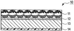
首先,如图1A所示,准备层叠膜10,该层叠膜10在透明基材13的一个面上具备透明电极层12、以及电泳显示层11,该电泳显示层11通过将封入了分散液的微胶囊用粘合剂树脂固定而成,该分散液通过将电泳粒子分散在分散介质中而成;在另一个面上具备接受层14。此外,如图1B所示,准备基板20,该基板20具备像素电极21和像素对位用的对准标记22。First, as shown in FIG. 1A, a laminated
接着,如图1C所示,将层叠膜10的电泳显示层11和基板20的像素电极21通过粘接层30贴合。此时,层叠膜10与基板20以在基板上的对准标记22的上部没有配置不透明的电泳显示层11的方式而贴合。Next, as shown in FIG. 1C , the
接着,如图1D所示,对于接受层14将两种以上的墨水通过喷墨印刷法吐出,在接受层14中形成彩色滤光片层。在图1D中,形成了红色彩色滤光片层15a、蓝色彩色滤光片层15b、绿色彩色滤光片层15c。在形成彩色滤光片层时,需要使基板20上的像素电极21图案与彩色滤光片层15a、15b、15c相对应。在有关本实施方式的电泳显示装置的制造方法中,通过以在基板上的对准标记22的上部不配置不透明的电泳显示层的方式使层叠膜10与基板20贴合,在使层叠膜10与基板20贴合后的彩色滤光片层15a、15b、15c的形成工序中,能够以基板上的对准标记22为基准,容易地形成与像素电极的图案对应的彩色滤光片层15a、15b、15c的图案。Next, as shown in FIG. 1D , two or more kinds of inks are discharged on the receiving
最后,如图1E所示,在接受层14及彩色滤光片层15a、15b、15c上设置保护膜40,制造电泳显示装置。Finally, as shown in FIG. 1E , a
接着,参照图2A~22F对有关本发明的第2实施方式的电泳式显示装置的制造方法进行说明。Next, a method of manufacturing an electrophoretic display device according to a second embodiment of the present invention will be described with reference to FIGS. 2A to 22F .
首先,如图2A所示,准备层叠膜10,该层叠膜10在透明基材13的一个面上具备透明电极层12,以及电泳显示层11,该电泳显示层11通过将封入了分散液的微胶囊用粘合剂树脂固定而成,该分散液通过将电泳粒子分散在分散介质中而成。此外,如图2B所示,准备基板20,该基板20具备像素电极21和像素对位用的图样(对准标记)22。First, as shown in FIG. 2A , a
接着,如图2C所示,将层叠膜10的电泳显示层11和基板20的像素电极21通过粘接层30贴合。此时,层叠膜10与基板20以在基板上的对准标记22的上部没有配置不透明的电泳显示层11的方式而贴合。Next, as shown in FIG. 2C , the
接着,如图2D所示,在层叠膜的透明基材表面上形成接受层14。Next, as shown in FIG. 2D, a
接着,如图2E所示,对于接受层14将两种以上的墨水通过喷墨印刷法吐出,在接受层14中形成彩色滤光片层。在图2E中,形成了红色彩色滤光片层15a、蓝色彩色滤光片层15b、绿色彩色滤光片层15c。在形成彩色滤光片层时,需要使基板20上的像素电极21图案与彩色滤光片层15a、15b、15c相对应。在有关本实施方式的电泳显示装置的制造方法中,通过以在基板上的对准标记22的上部不配置不透明的电泳显示层的方式使层叠膜10与基板20贴合,在使层叠膜10与基板20贴合后的彩色滤光片层15a、15b、15c的形成工序中,能够以基板上的对位用的图样为基准,容易地形成与像素电极的图案对应的彩色滤光片层15a、15b、15c的图案。Next, as shown in FIG. 2E , two or more kinds of inks are ejected to the receiving
最后,如图2F所示,在接受层14及彩色滤光片层15a、15b、15c上设置保护膜40,制造电泳显示装置。Finally, as shown in FIG. 2F, a
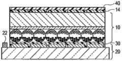
在图3中,表示根据以上说明的有关本发明的第1及第2实施方式的电泳显示装置的制造方法而制造的、有关本发明的第3实施方式的电泳显示装置的示意剖视图。FIG. 3 is a schematic cross-sectional view of an electrophoretic display device according to a third embodiment of the present invention manufactured by the methods of manufacturing the electrophoretic display device according to the first and second embodiments of the present invention described above.
在图3所示的电泳显示装置中,在具备像素电极21的基板20上经由粘接层30依次具备:电泳显示层11,该电泳显示层11通过将封入了分散液的微胶囊用粘合剂树脂固定而成,该分散液通过将电泳粒子分散在分散介质中而成;透明电极层12;透明基材13;具备彩色滤光片层15a、15b、15c的接受层以及保护膜。此时,隔着电泳显示层而设置的彩色滤光片层15a、15b、15c以与像素电极21的图案对置的方式而设置。通过针对各层的层叠方向使像素电极21图案与彩色滤光片层15a、15b、15c一致,能够进行多色显示(彩色显示)。在图3所示的电泳显示装置中,也可以在电泳显示层的侧面上设置用来防止向电泳显示层的水分的渗入的封固层50。In the electrophoretic display device shown in FIG. 3 , an
接着,对如以上那样构成的电泳显示装置的动作原理进行说明。Next, the principle of operation of the electrophoretic display device configured as above will be described.
基板20的像素电极21连接在各个像素电极的开关元件(未图示)上,能够在其与透明电极层12之间施加正负的电压。为了进行图像显示,通常像素电极21连接在有源矩阵型驱动方式的电路结构的电源上。如果对像素电极21施加电压,则作用在微胶囊层11上的电场变动。当像素电极21为正极时,微胶囊内的带电为负的粒子向背面的像素电极21的一侧移动,带电为正的粒子向前面的透明电极层12的一侧移动。同样,如果像素电极21为负极,则带电为正的粒子向像素电极21的一侧移动,带电为负的粒子向透明电极层12的一侧移动。这里,例如如果使黑色粒子带电为正、白色粒子带电为负,则显示色成为向前面的透明电极层12的一侧移动的粒子的颜色,所以通过来自观察侧的光在其上反射、反射光穿过对置的彩色滤光片层的着色图案,能够将希望的字符及图像进行颜色显示。The
在有关以上的实施方式的电泳显示装置及其制造方法中,在透明基材13上直接形成接受层14及彩色滤光片层15a、15b、15c。因而,在电泳层11与彩色滤光片层15a、15b、15c之间,仅存在透明电极层12和透明基材13。由于透明电极层12的厚度是亚微米量级,所以电泳显示层11与彩色滤光片层15a、15b、15c的距离根据透明基材13的厚度决定。因而,通过使透明基材13的厚度变小,能够使其距离接近,能够做成即使在从斜方向观察的情况下色彩变化也较小的能够进行多色显示的电泳显示装置。In the electrophoretic display device and its manufacturing method according to the above embodiments, the receiving
在以上的实施方式中,优选为:配置在透明基材13上的彩色滤光片层15a、15b、15c通过针对形成在透明基材13的表面上的接受层14用喷墨印刷法吐出多个颜色的墨水来形成。当在透明基材13上对彩色滤光片层15a、15b、15c进行图案形成时,在喷墨印刷法以外还可以进行通过光刻法的图案形成、通过胶版印刷法的图案形成。在这些方法中,也通过进行基于基板20的对准标记22的对位,能够在透明基材13上形成与像素电极21相对应的彩色滤光片层15a、15b、15c。In the above embodiments, it is preferable that the
在有关以上实施方式的电泳显示装置的制造方法中,其特征为在将层叠膜10与基板20贴合后形成彩色滤光片层15a、15b、15c,如果考虑层叠膜10与基板20贴合后的结构的操作性,优选为:彩色滤光片层15a、15b、15c通过用喷墨印刷法将多个颜色的墨水吐出而形成。通过用喷墨印刷法形成彩色滤光片,与其他图案形成方法相比,能够使像素电极21的图案与彩色滤光片层15a、15b、15c的图案的对位变容易。In the manufacturing method of the electrophoretic display device related to the above embodiment, it is characterized in that the
此外,在有关以上的实施方式的电泳显示装置及其制造方法中,优选为:在彩色滤光片层15a、15b、15c上层叠保护膜。通过设置保护膜,能够提高电泳显示装置的耐擦伤性。In addition, in the electrophoretic display device and its manufacturing method according to the above embodiments, it is preferable to laminate a protective film on the
此外,在有关以上的实施方式的电泳显示装置及其制造方法中,优选为:使透明基材13的厚度为10μm以上且100μm以下的范围内。如上述那样,在以上的实施方式中,电泳显示层11与彩色滤光片的距离根据透明基材13的厚度决定,所以能够使该距离接近,能够做成即使在从斜方向观察的情况下色彩变化也小的能够进行多色显示的电泳显示装置。In addition, in the electrophoretic display device and its manufacturing method according to the above embodiments, it is preferable that the thickness of the
这里,在透明基材13的厚度为超过100μm的厚度的情况下,就不能使本实施方式的效果成为充分的效果。另一方面,在透明基材13的厚度低于10μm的情况下,在透明基材13上的接受层14及微胶囊层11的形成时,由于层形成时的伸缩引起的透明基材13的变形大等的加工性较低、此外容易发生因透明基材13的变形引起的显示图像的不匀称。Here, when the thickness of the
以下,将进一步详细说明有关本发明的实施方式的电泳显示装置的制造方法及电泳显示装置。Hereinafter, the method for manufacturing the electrophoretic display device and the electrophoretic display device according to the embodiments of the present invention will be further described in detail.
可以使用聚对苯二甲酸乙二酯(PET)或聚碳酸酯、聚酰亚胺、聚萘二甲酸乙二醇酯、聚醚砜、丙烯树脂、聚氯乙烯等的塑料膜、或者玻璃等作为在有关本发明的实施方式的电泳显示装置中使用的透明基材13。Plastic films such as polyethylene terephthalate (PET), polycarbonate, polyimide, polyethylene naphthalate, polyethersulfone, acrylic resin, polyvinyl chloride, or glass can be used As the
在透明基材13上形成透明电极层12。可以使用ITO等的氧化铟类、氧化锡类、氧化锌类那样的具有透明性的导电性氧化物、或者碳纳米管或噻吩类化合物等作为透明电极形成材料。在透明电极层12的形成中,可以使用蒸镀法、溅射法、CVD法等的干式成膜法、或使用涂敷液的湿式成膜法等的以往技术。The
在透明电极层12上形成将微胶囊用粘合剂树脂固定的电泳显示层11。电泳显示层11通过将包含有封入了将电泳粒子分散在分散介质中的微胶囊、粘合剂树脂、以及溶媒的电泳层形成用涂敷液涂敷到具备透明电极12的透明基材13上而形成。On the
微胶囊型电泳层11的形成中所使用的微胶囊具备如下的构造:在微胶囊壳内至少电极性不同的两种粒子被分散在透明的分散介质中。The microcapsules used for forming the microcapsule-
作为被封入到微胶囊内的电极性不同的两种粒子,可以举出黑色粒子与白色粒子的组合。微胶囊优选为:通过筛分法或比重分离法等精制、使用平均粒径为30~100μm的微胶囊。此外,优选为:相对于微胶囊的平均粒径具有前后10μm以内的粒径的微胶囊的比例至少超过50%。Examples of the two types of particles with different electric polarities enclosed in the microcapsules include a combination of black particles and white particles. The microcapsules are preferably purified by a sieving method, a specific gravity separation method, or the like, and those having an average particle diameter of 30 to 100 μm are used. In addition, it is preferable that the proportion of microcapsules having particle diameters within 10 μm or less relative to the average particle diameter of the microcapsules exceeds at least 50%.
微胶囊分散液使用乙醇等的水系溶剂,如果没有特别的问题,则使用水。例如使用脂肪族烃、芳香族烃、脂环族烃、卤化烃、各种酯类、乙醇类溶媒、或将其他脂等单独或适当混合的溶媒作为透明分散介质。Aqueous solvents such as ethanol are used for the microcapsule dispersion liquid, and water is used if there is no particular problem. For example, aliphatic hydrocarbons, aromatic hydrocarbons, alicyclic hydrocarbons, halogenated hydrocarbons, various esters, ethanol-based solvents, or solvents in which other lipids are used alone or in proper mixture are used as transparent dispersion media.
在黑色粒子中,除了无机碳等的无机颜料以外,还可以使用玻璃或树脂等的微粉末、还有它们的复合体等。另一方面,可以使用周知的氧化钛、二氧化硅、氧化铝、氧化锌等的白色无机颜料、醋酸乙烯乳胶等的有机化合物、还有它们的复合体等作为白色粒子。As the black particles, in addition to inorganic pigments such as inorganic carbon, fine powders such as glass or resin, and composites thereof can be used. On the other hand, well-known white inorganic pigments such as titanium oxide, silica, aluminum oxide, and zinc oxide, organic compounds such as vinyl acetate latex, and complexes thereof can be used as white particles.
另外,黑色粒子及白色粒子不仅可以根据需要而通过使用各种界面活性剂、分散剂、有机及无机化合物、金属等对粒子的表面进行处理从而赋予期望的表面电荷,还能够提高分散介质中的分散稳定性。In addition, black particles and white particles can not only give desired surface charges by using various surfactants, dispersants, organic and inorganic compounds, metals, etc. to treat the surface of the particles as needed, but also improve the dispersion medium. dispersion stability.
将分散了微胶囊的分散液使用混合凝聚法等的相分离法、界面聚合法、in-situ法、熔化分散冷凝法等周知的方法封入到微胶囊胶囊壳中,成为微胶囊。例如可以使用橡胶或明胶作为微胶囊壳。The dispersion liquid in which microcapsules are dispersed is encapsulated in a microcapsule shell by a known method such as a phase separation method such as a mixing coagulation method, an interfacial polymerization method, an in-situ method, and a melting dispersion condensation method to form microcapsules. For example rubber or gelatin can be used as the microcapsule shell.
可以使用聚乳酸、酚醛树脂、聚丙烯树脂、丙烯树脂等的电介体树脂作为在电泳层形成用涂敷液中含有的粘合剂树脂。Dielectric resins such as polylactic acid, phenolic resin, polypropylene resin, and acrylic resin can be used as the binder resin contained in the coating liquid for forming an electrophoretic layer.
可以使用丝网印刷方式、微型凹版涂布机、吻涂涂布机、逗号型涂布机、模具型涂布机、棒式涂布机、帘式涂布机等的涂敷装置作为电泳层形成用涂敷液的涂敷方法来进行。在电泳层形成用涂敷液被涂敷后,将透明电极层上的涂敷液干燥。可以使用加入、送风等作为干燥方法。Coating equipment such as screen printing, micro gravure coater, kiss coater, comma coater, die coater, rod coater, curtain coater, etc. can be used as the electrophoretic layer Formation is performed by a coating method of a coating liquid. After the coating liquid for forming the electrophoretic layer is applied, the coating liquid on the transparent electrode layer is dried. Addition, air blowing, etc. can be used as a drying method.
在有关本发明的实施方式的电泳显示装置的制造方法中,将具备像素电极21的基板20的像素电极表面与层叠膜10的电泳显示层表面经由粘接剂层30而贴合,该层叠膜10在透明基材13上具备透明电极层12及电泳显示层11。此时,能够作为粘接剂使用的,优选使用氨基甲酸乙酯树脂类粘接剂、丙烯树脂类粘接剂等的合成树脂类粘接剂。特别优选使用的是采用高电介体树脂的粘接剂。In the method of manufacturing an electrophoretic display device according to the embodiment of the present invention, the surface of the pixel electrode of the
在透明基材13的与电泳层形成面相反侧的面上,设有彩色滤光片层15a、15b、15c。彩色滤光片层15a、15b、15c通过形成接受层14且在该接受层14上涂敷多种墨水而形成。另外,接受层14既可以如图1A~1E所示那样在将层叠膜10与基板20贴合之前设置,也可以如图2A~2F所示那样在将层叠膜10与基板20贴合之后设置。Color filter layers 15 a , 15 b , and 15 c are provided on the surface of the
在将层叠膜10与基板20贴合之前设置接受层14的情况下,由于能够采用辊对辊(roll-to-roll)方式通过连续涂敷形成接受层14,所以为优选。但是,存在需要用来保护接受层14的覆盖膜的情况。另一方面,在将层叠膜10与基板20贴合之后设置接受层14的情况下,由于能够连续进行接受层14的形成和彩色滤光片层15a、15b、15c的形成,所以不需要使用覆盖膜等,而为优选。When the receiving
接受层14通过将含有树脂的接受层形成用涂敷液涂敷到透明基材13上而形成。可以使用氨基甲酸乙酯树脂、聚酯、丙烯树脂、乙烯醇树脂等作为接受层14的材质。此外,为了提高墨水的溶媒的吸收性而也可以使接受层14中含有合成二氧化硅或氧化铝等的多孔质物质。接受层14的形成只要是进行单晶圆处理方式,就可以通过丝网印刷法、胶版印刷法、旋涂法、通过模具的间歇涂敷来形成。此外,如果是进行辊对辊(roll-to-roll)的连续处理,则能够通过模具涂敷、逗号型涂敷、帘型涂敷、凹版涂敷等的通用的涂敷技术而形成接受层。此外,在接受层形成用涂敷液被涂敷后,将透明基材13上的涂敷液干燥。可以使用加热、送风等作为干燥方法。The receiving
可以使用含有周知的着色颜料或着色染料的墨水作为用来形成彩色滤光片层15a、15b、15c的墨水。彩色滤光片层15a、15b、15c是按照像素将光着色的,可以使用红色(R)、绿色(G)、蓝色(B)的三色图案、或者黄色(Y)、品红色(M)、青色(C)的3色的图案。此外,也可以是这些颜色的组合,此外,也可以组合白色(W)等的其他颜色。As the ink for forming the
如果具体地举出着色颜料的成分,则在用来形成红色着色层或红色像素的红色着色组成物中,可以使用例如C.I.Pigment Red7,9,14,41,48:1,48:2,48:3,48:4,81:1,81:2,81:3,97,122,123,146,149,168,177,178,179,180,184,185,187,192,200,202,208,210,215,216,217,220,223,224,226,227,228,240,246,254,255,264,272,279等的红色颜料。在红色着色组成物中,可以添加并用黄色颜料、橙色颜料。If the components of the coloring pigment are mentioned specifically, in the red coloring composition for forming the red coloring layer or the red pixel, for example, C.I. Pigment Red7, 9, 14, 41, 48:1, 48:2, 48 can be used : 3, 48: 4, 81: 1, 81: 2, 81: 3, 97, 122, 123, 146, 149, 168, 177, 178, 179, 180, 184, 185, 187, 192, 200, 202 , 208, 210, 215, 216, 217, 220, 223, 224, 226, 227, 228, 240, 246, 254, 255, 264, 272, 279 and other red pigments. In the red coloring composition, a yellow pigment and an orange pigment can be added and used.
在绿色着色组成物中,可以使用例如C.I.Pigment Green7,10,36,37等的绿色颜料。在绿色着色组成物中,可以添加并用与红色着色组成物同样的黄色颜料。In the green coloring composition, green pigments such as C.I.
在蓝色着色组成物中,可以使用例如C.I.Pigment Blue15,15:1,15:2,15:3,15:4,15:6,16,22,60,64,80等的蓝色颜料,优选使用C.I.Pigment Blue15:6。此外,在蓝色着色组成物中,可以添加并用C.I.Pigment Violet1,19,23,27,29,30,32,37,40,42,50等的紫色颜料,优选添加并用C.I.Pigment Violet23。In the blue coloring composition, blue pigments such as C.I.Pigment Blue15, 15:1, 15:2, 15:3, 15:4, 15:6, 16, 22, 60, 64, 80, etc. can be used, Preferably C.I. Pigment Blue 15:6 is used. In addition, purple pigments such as C.I.
在构成有关本发明的实施方式的电泳显示装置的彩色滤光片层15a、15b、15c中,没有形成用来将每个像素用黑色分隔的黑色矩阵。有关本发明的实施方式的电泳显示装置的彩色滤光片层由于不形成黑色矩阵,所以在形成彩色滤光片层15a、15b、15c时形成透明的接受层14、在该透明的接受层14中通过喷墨印刷法吐出墨水而形成彩色滤光片的方法生产性较高,可以优选采用。In the color filter layers 15 a , 15 b , and 15 c constituting the electrophoretic display device according to the embodiment of the present invention, a black matrix is not formed for dividing each pixel into black. Since the color filter layer of the electrophoretic display device according to the embodiment of the present invention does not form a black matrix, a
由于需要根据颜色分开涂敷,所以可以使用丝网印刷法、胶版印刷法、喷墨印刷法等作为接受层14的墨水的涂敷方法。其中,由于对位容易,所以优选使用喷墨印刷法向接受层14吐出墨水而形成彩色滤光片层。Since it is necessary to apply separately according to the color, a screen printing method, an offset printing method, an inkjet printing method, or the like can be used as a method of applying the ink of the receiving
作为具备像素电极21的基板20,可以使用周知的结构。基板20的像素电极21连接在各个像素电极的开关元件上,在其与透明电极层12之间能够施加正负的电压。像素电极21连接在有源矩阵型驱动方式的电路结构的电源上。A well-known structure can be used as the
作为设置在基板20的像素电极面上的对准标记22,可以使用在基板20的像素电极面的端部上通过墨水图案形成的对准标记。此外,也可以在基板20上的像素电极面的端部上形成虚拟的像素电极图案而作为对准标记22。也可以在像素电极制作时同时形成虚拟图案。此外,也可以将基板20的像素电极形成面的配线图案或虚拟的配线图案作为对准标记22。作为对准标记22的形状,可以举出十字形、圆形、多重同心圆形、楔形等。As the
作为保护膜,可以使用在透明基材中表示的材料,可以使用聚对苯二甲酸乙二酯(PET)或聚碳酸酯、聚酰亚胺、聚萘二甲酸乙二醇酯、聚醚砜、丙烯树脂、聚氯乙烯等的塑料膜、或者玻璃等。此外,在保护膜中,也可以在观察者侧设置用来提高表面的耐擦伤性的硬涂层、或用来防止表面的反射的防反射层、含有考虑到防湿性的金属成分的薄膜层。另外,接受层和保护膜通过周知的粘接剂贴合。As the protective film, the materials shown in the transparent substrate can be used, and polyethylene terephthalate (PET) or polycarbonate, polyimide, polyethylene naphthalate, polyethersulfone can be used , plastic film such as acrylic resin or polyvinyl chloride, or glass. In addition, in the protective film, a hard coat layer for improving the scratch resistance of the surface, an anti-reflection layer for preventing reflection on the surface, or a thin film containing a metal component in consideration of moisture resistance may be provided on the viewer side. layer. In addition, the receiving layer and the protective film are bonded together with a known adhesive.
作为将隔着上述微胶囊层11的电极板的端部封固的树脂,可以举出作为热塑性树脂的聚烯烃树脂、聚酯树脂、聚酰胺树脂、聚氨酯树脂、聚硅树脂类的密封剂或者作为热硬化性树脂的环氧树脂、聚氨酯树脂、三聚氰胺树脂、酚醛树脂、丙烯树脂类的密封剂等。As the resin that seals the end of the electrode plate via the
实施例Example
<实施例1><Example 1>
将用聚乙烯树脂覆盖了表面的平均粒径3μm的氧化钛粉末(白色粒子)、和用烷基三甲基氯化铵进行表面处理后的平均粒径4μm的炭黑粉末(黑色粒子)分散到四氯乙烯中,得到分散液。在此情况下,通过电场的施加,白色粒子带电为负,黑色粒子带电为正。Disperse titanium oxide powder (white particles) with an average particle size of 3 μm covered with polyethylene resin and carbon black powder (black particles) with an average particle size of 4 μm after surface treatment with alkyltrimethylammonium chloride into tetrachloroethylene to obtain a dispersion. In this case, the white particles are negatively charged and the black particles are positively charged by the application of the electric field.
将该分散液O/W乳胶化,通过用明胶-阿拉伯橡胶的复合·凝聚法而形成微胶囊,将上述分散液封入到微胶囊中。This dispersion liquid was O/W emulsified, and microcapsules were formed by the composite/agglomeration method of gelatin-rubber arabic, and the above-mentioned dispersion liquid was encapsulated in the microcapsules.
将这样得到的微胶囊筛分,以使平均粒径为60μm、50~70μm的粒径的微胶囊的比例为50%以上的方式而使粒径一致。The microcapsules thus obtained were sieved so that the particle diameters were uniform so that the proportion of microcapsules with an average particle diameter of 60 μm and a particle diameter of 50 to 70 μm was 50% or more.
接着,调制出固体成分40质量%的微胶囊的水分散液。将该水分散液、固体成分25质量%的聚氨酯类粘合剂(CP-7050,大日本墨水株式会社制)、界面活性剂、增粘剂以及纯水混合,调制出电泳层形成用涂敷液。Next, an aqueous dispersion of microcapsules having a solid content of 40% by mass was prepared. This aqueous dispersion, a polyurethane-based adhesive with a solid content of 25% by mass (CP-7050, manufactured by Dainippon Ink Co., Ltd.), a surfactant, a thickener, and pure water were mixed to prepare a coating for forming an electrophoretic layer. liquid.
然后,在ITO层/PET膜的PET侧使用逗号型涂布机连续涂敷聚酯树脂类的接受液NS-141LX(高松油脂株式会社),形成平均膜厚10μm的接受层。将聚丙烯膜基底的L-5005(日立化成株式会社)作为暂时保护接受层的膜而贴合在接受层上,得到由暂时的保护膜/接受层/PET膜/ITO层构成的多层膜。Then, a polyester resin-based receiver liquid NS-141LX (Takamatsu Shishishi Co., Ltd.) was continuously coated on the PET side of the ITO layer/PET film using a comma coater to form a receiver layer with an average film thickness of 10 μm. Polypropylene film-based L-5005 (Hitachi Chemical Co., Ltd.) was bonded to the receptor layer as a film to temporarily protect the receptor layer to obtain a multilayer film consisting of temporary protective film/receptor layer/PET film/ITO layer .
接着,将上述微胶囊墨水向多层膜的ITO层侧通过模具涂敷为75μm厚,在形成的微胶囊层的表面上贴合带有聚氨酯类粘接剂的Si剥离层膜,得到由暂时的保护膜/接受层/PET膜/ITO层/微胶囊型电泳显示层/Si剥离层构成的层叠膜。Next, the above-mentioned microcapsule ink is applied to the ITO layer side of the multilayer film to a thickness of 75 μm by die coating, and a Si release layer film with a polyurethane adhesive is attached on the surface of the formed microcapsule layer to obtain a temporary Laminated film composed of protective film/accepting layer/PET film/ITO layer/microcapsule electrophoretic display layer/Si peeling layer.
层叠膜从卷绕了得到的带有接受层的层叠膜的辊拉出,使用CO2激光切割装置,被裁剪为比具备像素电极的基板小的尺寸。The laminated film was pulled out from a roll on which the obtained laminated film with a receiving layer was wound, and was cut to a size smaller than the substrate having the pixel electrode using a CO2 laser cutting device.
另一方面,准备在表面上形成有像素电极和对准标记的基板。像素电极具有使用薄膜晶体管的有源矩阵型驱动方式的电路结构。此外,对准标记形成在基板表面的端部上,为总宽度500μm线宽度200μm的十字图样。On the other hand, a substrate on which pixel electrodes and alignment marks are formed on the surface is prepared. The pixel electrodes have a circuit structure of an active matrix driving method using thin film transistors. In addition, an alignment mark was formed on the end portion of the substrate surface in a cross pattern with a total width of 500 μm and a line width of 200 μm.
接着,将裁剪后的层叠膜的Si剥离膜剥离(粘接剂附着在微胶囊型电泳显示层上),在剥离后的面上通过层压而贴合上述在表面上形成有像素电极和对准标记的基板,从而得到带有接受层的电泳微胶囊基板。Next, the Si peeling film of the laminated film after cutting is peeled off (adhesive is attached to the microcapsule type electrophoretic display layer), and the above-mentioned pixel electrode and counter electrode formed on the surface are bonded by lamination on the peeled surface. quasi-marked substrates to obtain electrophoretic microcapsule substrates with a receiving layer.
将得到的带有接受层的电泳微胶囊基板的接受层侧的暂时的保护膜剥离,针对接受层通过喷墨印刷按照像素进行分色印刷,形成彩色滤光片层。此时,通过基板上的对位用的十字图样进行对位。此外,彩色滤光片层为红、蓝、绿的图案。The temporary protective film on the receiving layer side of the obtained electrophoretic microcapsule substrate with a receiving layer was peeled off, and color separation printing was performed on the receiving layer by inkjet printing for each pixel to form a color filter layer. At this time, alignment is performed by the cross pattern for alignment on the substrate. In addition, the color filter layer has patterns of red, blue and green.
接着,将带粘着的硬涂膜KB Stick SG90R(KBスティックSG90R)(株式会社木本、即株式会社きもと)作为保护膜而层压到接受层上。通过以上制作出电泳显示装置。Next, an adhesive hard coat film KB Stick SG90R (KB Stick SG90R) (Kimoto Co., Ltd., Kimoto Co., Ltd.) was laminated on the receiving layer as a protective film. An electrophoretic display device was fabricated as described above.
对得到的电泳显示装置的各像素施加电压,能够进行彩色的显示。此外,由于电泳层与彩色滤光片层接近,所以观察不到因视差带来的颜色不匀。By applying a voltage to each pixel of the obtained electrophoretic display device, color display can be performed. In addition, since the electrophoretic layer is close to the color filter layer, color unevenness due to parallax cannot be observed.
<实施例2><Example 2>
将用聚乙烯树脂覆盖了表面的平均粒径3μm的氧化钛粉末(白色粒子)、和用烷基三甲基氯化铵进行表面处理后的平均粒径4μm的炭黑粉末(黑色粒子)分散到四氯乙烯中,得到分散液。在此情况下,通过电场的施加,白色粒子带电为负,黑色粒子带电为正。Disperse titanium oxide powder (white particles) with an average particle size of 3 μm covered with polyethylene resin and carbon black powder (black particles) with an average particle size of 4 μm after surface treatment with alkyltrimethylammonium chloride into tetrachloroethylene to obtain a dispersion. In this case, the white particles are negatively charged and the black particles are positively charged by the application of the electric field.
将该分散液O/W乳胶化,通过用明胶-阿拉伯橡胶的复合·凝聚法而形成微胶囊,将上述分散液封入到微胶囊中。This dispersion liquid was O/W emulsified, and microcapsules were formed by the composite/agglomeration method of gelatin-rubber arabic, and the above-mentioned dispersion liquid was encapsulated in the microcapsules.
将这样得到的微胶囊筛分,以使平均粒径为60μm、50~70μm的粒径的微胶囊的比例为50%以上的方式而使粒径一致。The microcapsules thus obtained were sieved so that the particle diameters were uniform so that the proportion of microcapsules with an average particle diameter of 60 μm and a particle diameter of 50 to 70 μm was 50% or more.
接着,调制出固体成分40质量%的微胶囊的水分散液。将该水分散液、固体成分25质量%的聚氨酯类粘合剂(CP-7050,大日本墨水株式会社制)、界面活性剂、增粘剂以及纯水混合,调制出电泳层形成用涂敷液。Next, an aqueous dispersion of microcapsules having a solid content of 40% by mass was prepared. This aqueous dispersion, a polyurethane-based adhesive with a solid content of 25% by mass (CP-7050, manufactured by Dainippon Ink Co., Ltd.), a surfactant, a thickener, and pure water were mixed to prepare a coating for forming an electrophoretic layer. liquid.
将该电泳层形成用涂敷液使用狭缝模具涂布机涂敷到膜的ITO层上,该膜由100μm的厚度的ITO层/PET基材而构成,涂敷后在60℃下干燥10分钟,得到由微胶囊型电泳显示层/ITO层/PET膜构成的层叠膜。The coating solution for forming the electrophoretic layer was applied to the ITO layer of a film made of an ITO layer/PET base material with a thickness of 100 μm using a slot die coater, and dried at 60° C. for 10 days after coating. Minutes, a laminated film composed of microcapsule electrophoretic display layer/ITO layer/PET film is obtained.
层叠膜从卷绕了得到的层叠膜的辊拉出,使用CO2激光切割装置,被裁剪为比具备像素电极的基板小的尺寸。The laminated film was pulled out from a roll on which the obtained laminated film was wound, and cut to a size smaller than the substrate having the pixel electrodes using a CO2 laser cutting device.
另一方面,准备在表面上形成有像素电极和对准标记的基板。像素电极具有使用薄膜晶体管的有源矩阵型驱动方式的电路结构。此外,对准标记形成在基板表面的端部上,为直径500μm和200μm的、线宽度100μm的二重同心圆形图样。On the other hand, a substrate on which pixel electrodes and alignment marks are formed on the surface is prepared. The pixel electrodes have a circuit structure of an active matrix driving method using thin film transistors. In addition, alignment marks were formed on the ends of the substrate surface as double concentric circular patterns of 500 μm and 200 μm in diameter and 100 μm in line width.
接着,将裁剪后的层叠膜以0.50MP的压力贴合到基板的像素电极面上,制作出电泳显示面板。此时,以使得在基板的像素对位用的图样上不配置层叠膜的方式进行贴合。Next, the laminated film after cutting was bonded to the pixel electrode surface of the substrate with a pressure of 0.50 MP, to manufacture an electrophoretic display panel. At this time, bonding is carried out so that the laminated film is not disposed on the pattern for pixel alignment on the substrate.
将得到的电泳显示面板的像素电极和层叠膜的层叠端部用UV硬化型的封固剂KJC-7805(信越化学株式会社)包围、封固。The pixel electrode of the obtained electrophoretic display panel and the laminated end of the laminated film were surrounded and sealed with a UV-curable sealing agent KJC-7805 (Shin-Etsu Chemical Co., Ltd.).
接着,通过用模头将作为喷墨用接受液的喷墨受像用涂层剂IJ-2101(DAIALLOMER IJ2101、即ダイアロマーIJ-2101)(大日精化工业株式会社)间歇地涂敷到透明基材上,形成约10μm膜厚的接受层。Next, the inkjet image receiving coating agent IJ-2101 (DAIALLOMER IJ2101, ie Dialomar IJ-2101) (Dainichi Seika Kogyo Co., Ltd.), which is the inkjet receiving liquid, is intermittently applied to the transparent substrate by using a die head. On top, a receptor layer with a film thickness of about 10 μm was formed.
对上述接受层,以处于基板端部的对位图样为基准,使用喷墨装置印刷与各像素对应的颜色的墨,形成彩色滤光片层。此时,以基板上的对位用的二重同心圆形图样为基准进行对位。此外,彩色滤光片层为红、蓝、绿的图案。接着,将带有粘着剂的硬涂膜(KB Stick SG90R、即KBスティックSG90R:株式会社木本制、即株式会社きもと制)作为保护膜层压到接受层上。通过以上,制作出电泳显示装置。On the receiving layer, ink of a color corresponding to each pixel was printed using an inkjet device based on the alignment pattern at the edge of the substrate to form a color filter layer. At this time, alignment is performed based on the double concentric circular pattern for alignment on the substrate. In addition, the color filter layer has patterns of red, blue and green. Next, a hard coat film (KB Stick SG90R, KB Stick SG90R: manufactured by Kimoto Co., Ltd., manufactured by Kimoto Co., Ltd.) with an adhesive was laminated on the receiving layer as a protective film. Through the above, an electrophoretic display device was produced.
然后,对各像素施加电压,能够进行彩色的显示。此外,由于电泳层与彩色滤光片层接近,所以观察不到因视差带来的颜色不匀。Then, a voltage is applied to each pixel to perform color display. In addition, since the electrophoretic layer is close to the color filter layer, color unevenness caused by parallax is not observed.
Claims (13)
Translated fromChineseApplications Claiming Priority (3)
| Application Number | Priority Date | Filing Date | Title |
|---|---|---|---|
| JP2011-027015 | 2011-02-10 | ||
| JP2011027015AJP5817134B2 (en) | 2011-02-10 | 2011-02-10 | Method for manufacturing electrophoretic display device and electrophoretic display device |
| PCT/JP2012/052745WO2012108431A1 (en) | 2011-02-10 | 2012-02-07 | Electrophoretic display device and method for producing same |
Publications (2)
| Publication Number | Publication Date |
|---|---|
| CN103348284Atrue CN103348284A (en) | 2013-10-09 |
| CN103348284B CN103348284B (en) | 2016-09-07 |
Family
ID=46638644
Family Applications (1)
| Application Number | Title | Priority Date | Filing Date |
|---|---|---|---|
| CN201280008342.7AExpired - Fee RelatedCN103348284B (en) | 2011-02-10 | 2012-02-07 | Electrophoretic display device and manufacturing method thereof |
Country Status (7)
| Country | Link |
|---|---|
| US (2) | US9664977B2 (en) |
| EP (1) | EP2674810B1 (en) |
| JP (1) | JP5817134B2 (en) |
| KR (1) | KR101571228B1 (en) |
| CN (1) | CN103348284B (en) |
| TW (2) | TWI627485B (en) |
| WO (1) | WO2012108431A1 (en) |
Cited By (5)
| Publication number | Priority date | Publication date | Assignee | Title |
|---|---|---|---|---|
| CN103901693A (en)* | 2014-03-17 | 2014-07-02 | 华南师范大学 | Color electrophoresis electronic paper display thin film and manufacturing method thereof |
| CN104820318A (en)* | 2014-01-31 | 2015-08-05 | 精工爱普生株式会社 | Pixel electrode, display device, method of manufacturing pixel electrode |
| CN107831626A (en)* | 2017-10-31 | 2018-03-23 | 广州奥翼电子科技股份有限公司 | A kind of flexible color electrophoretic display and preparation method thereof |
| CN109298580A (en)* | 2018-12-12 | 2019-02-01 | 成都捷翼电子科技有限公司 | A color electrophoretic display module |
| CN112099284A (en)* | 2020-09-28 | 2020-12-18 | 京东方科技集团股份有限公司 | Display panel, display method thereof and display device |
Families Citing this family (14)
| Publication number | Priority date | Publication date | Assignee | Title |
|---|---|---|---|---|
| CN104321697A (en)* | 2012-08-21 | 2015-01-28 | 凸版印刷株式会社 | Reflective display panel and manufacturing method thereof |
| EP2853940B1 (en)* | 2012-08-22 | 2019-09-11 | Toppan Printing Co., Ltd. | Method for inspecting an electrophoretic display substrate |
| JP6287843B2 (en)* | 2012-10-04 | 2018-03-07 | 凸版印刷株式会社 | Reflective color display |
| TWI493270B (en)* | 2012-12-28 | 2015-07-21 | E Ink Holdings Inc | Display device and fabrication method of display device |
| TWI490614B (en)* | 2013-01-24 | 2015-07-01 | E Ink Holdings Inc | Electrophoretic display apparatus |
| JP6094244B2 (en)* | 2013-02-08 | 2017-03-15 | 凸版印刷株式会社 | Reflective display device and manufacturing method thereof |
| CN107688264A (en)* | 2016-08-05 | 2018-02-13 | 元太科技工业股份有限公司 | Electrophoretic display device |
| CN108508673A (en)* | 2018-04-03 | 2018-09-07 | 广州奥翼电子科技股份有限公司 | A kind of color monitor and preparation method thereof |
| US11055593B1 (en)* | 2020-01-07 | 2021-07-06 | Capital One Services, Llc | Providing alerts via a color changing transaction card |
| US11846863B2 (en) | 2020-09-15 | 2023-12-19 | E Ink Corporation | Coordinated top electrode—drive electrode voltages for switching optical state of electrophoretic displays using positive and negative voltages of different magnitudes |
| JP7542140B2 (en)* | 2020-09-15 | 2024-08-29 | イー インク コーポレイション | Four-particle electrophoretic medium providing fast and high contrast optical state switching |
| US12181767B2 (en) | 2020-09-15 | 2024-12-31 | E Ink Corporation | Five-particle electrophoretic medium with improved black optical state |
| WO2022060700A1 (en) | 2020-09-15 | 2022-03-24 | E Ink Corporation | Improved driving voltages for advanced color electrophoretic displays and displays with improved driving voltages |
| WO2024128548A1 (en)* | 2022-12-14 | 2024-06-20 | 삼성전자주식회사 | Home appliance and method for manufacturing same |
Citations (7)
| Publication number | Priority date | Publication date | Assignee | Title |
|---|---|---|---|---|
| US20040252360A1 (en)* | 2001-07-09 | 2004-12-16 | E Ink Corporation | Electro-optic display and lamination adhesive for use therein |
| US20050190431A1 (en)* | 2004-01-27 | 2005-09-01 | Canon Kabushiki Kaisha | Display apparatus and driving method thereof |
| JP2007322784A (en)* | 2006-06-01 | 2007-12-13 | Bridgestone Corp | Information display panel and its manufacturing method |
| CN101221338A (en)* | 2007-01-09 | 2008-07-16 | 三星Sdi株式会社 | Organic electrophoretic display device and manufacturing method thereof |
| CN101515103A (en)* | 2008-02-21 | 2009-08-26 | 精工爱普生株式会社 | Electrophoretic display device and method of manufacturing electrophoretic display device |
| JP2010503895A (en)* | 2006-09-18 | 2010-02-04 | イー インク コーポレイション | Color electro-optic display |
| US20110026099A1 (en)* | 2009-08-03 | 2011-02-03 | Oh-Nam Kwon | Electrophoretic display device and method of fabricating the same |
Family Cites Families (12)
| Publication number | Priority date | Publication date | Assignee | Title |
|---|---|---|---|---|
| JPS5015115A (en) | 1973-06-13 | 1975-02-18 | ||
| JP3372724B2 (en)* | 1994-09-21 | 2003-02-04 | キヤノン株式会社 | Color filter and manufacturing method thereof, liquid crystal panel, and information processing device |
| TW574523B (en)* | 2001-11-23 | 2004-02-01 | Ind Tech Res Inst | Color filter of liquid crystal display |
| KR20070007644A (en) | 2005-07-11 | 2007-01-16 | 박세룡 | Bath Heat Pump |
| TWI468472B (en) | 2006-01-13 | 2015-01-11 | Toyo Ink Mfg Co | Color filters are used for coloring compositions, color filters and liquid crystal display devices |
| TW200832031A (en)* | 2007-01-22 | 2008-08-01 | Gigno Technology Co Ltd | E-paper apparatus and manufacturing method thereof |
| JP5790968B2 (en)* | 2008-08-18 | 2015-10-07 | Nltテクノロジー株式会社 | Display device and manufacturing method thereof |
| KR101111112B1 (en) | 2009-04-21 | 2012-02-13 | 황장환 | Manufacturing Method of Image Display Device |
| KR20100073356A (en)* | 2008-12-23 | 2010-07-01 | 엘지디스플레이 주식회사 | Color electric phoretic display device and method for manufacturing the same |
| US8098418B2 (en)* | 2009-03-03 | 2012-01-17 | E. Ink Corporation | Electro-optic displays, and color filters for use therein |
| JP2010276986A (en)* | 2009-05-29 | 2010-12-09 | Bridgestone Corp | Transparent substrate with color filter, information display panel with color filter, and method for manufacturing the substrate and the panel |
| TWM485266U (en)* | 2014-05-06 | 2014-09-01 | Hocheng Corp | Improved external sewer device of toilet |
- 2011
- 2011-02-10JPJP2011027015Apatent/JP5817134B2/ennot_activeExpired - Fee Related
- 2012
- 2012-02-07CNCN201280008342.7Apatent/CN103348284B/ennot_activeExpired - Fee Related
- 2012-02-07EPEP12745303.3Apatent/EP2674810B1/ennot_activeNot-in-force
- 2012-02-07KRKR1020137021012Apatent/KR101571228B1/ennot_activeExpired - Fee Related
- 2012-02-07WOPCT/JP2012/052745patent/WO2012108431A1/enactiveApplication Filing
- 2012-02-09TWTW106114495Apatent/TWI627485B/ennot_activeIP Right Cessation
- 2012-02-09TWTW101104140Apatent/TWI615666B/ennot_activeIP Right Cessation
- 2013
- 2013-07-30USUS13/954,403patent/US9664977B2/ennot_activeExpired - Fee Related
- 2017
- 2017-04-27USUS15/499,394patent/US10416523B2/enactiveActive
Patent Citations (7)
| Publication number | Priority date | Publication date | Assignee | Title |
|---|---|---|---|---|
| US20040252360A1 (en)* | 2001-07-09 | 2004-12-16 | E Ink Corporation | Electro-optic display and lamination adhesive for use therein |
| US20050190431A1 (en)* | 2004-01-27 | 2005-09-01 | Canon Kabushiki Kaisha | Display apparatus and driving method thereof |
| JP2007322784A (en)* | 2006-06-01 | 2007-12-13 | Bridgestone Corp | Information display panel and its manufacturing method |
| JP2010503895A (en)* | 2006-09-18 | 2010-02-04 | イー インク コーポレイション | Color electro-optic display |
| CN101221338A (en)* | 2007-01-09 | 2008-07-16 | 三星Sdi株式会社 | Organic electrophoretic display device and manufacturing method thereof |
| CN101515103A (en)* | 2008-02-21 | 2009-08-26 | 精工爱普生株式会社 | Electrophoretic display device and method of manufacturing electrophoretic display device |
| US20110026099A1 (en)* | 2009-08-03 | 2011-02-03 | Oh-Nam Kwon | Electrophoretic display device and method of fabricating the same |
Cited By (7)
| Publication number | Priority date | Publication date | Assignee | Title |
|---|---|---|---|---|
| CN104820318A (en)* | 2014-01-31 | 2015-08-05 | 精工爱普生株式会社 | Pixel electrode, display device, method of manufacturing pixel electrode |
| CN103901693A (en)* | 2014-03-17 | 2014-07-02 | 华南师范大学 | Color electrophoresis electronic paper display thin film and manufacturing method thereof |
| CN103901693B (en)* | 2014-03-17 | 2017-06-30 | 华南师范大学 | A kind of color electrophoresis Electronic Paper shows film and its manufacture method |
| CN107831626A (en)* | 2017-10-31 | 2018-03-23 | 广州奥翼电子科技股份有限公司 | A kind of flexible color electrophoretic display and preparation method thereof |
| CN109298580A (en)* | 2018-12-12 | 2019-02-01 | 成都捷翼电子科技有限公司 | A color electrophoretic display module |
| CN112099284A (en)* | 2020-09-28 | 2020-12-18 | 京东方科技集团股份有限公司 | Display panel, display method thereof and display device |
| CN112099284B (en)* | 2020-09-28 | 2024-01-23 | 京东方科技集团股份有限公司 | Display panel, display method thereof and display device |
Also Published As
| Publication number | Publication date |
|---|---|
| US20130314764A1 (en) | 2013-11-28 |
| TW201736926A (en) | 2017-10-16 |
| CN103348284B (en) | 2016-09-07 |
| TWI627485B (en) | 2018-06-21 |
| JP2012168242A (en) | 2012-09-06 |
| US10416523B2 (en) | 2019-09-17 |
| JP5817134B2 (en) | 2015-11-18 |
| TWI615666B (en) | 2018-02-21 |
| WO2012108431A1 (en) | 2012-08-16 |
| KR101571228B1 (en) | 2015-11-23 |
| TW201239498A (en) | 2012-10-01 |
| US20170227827A1 (en) | 2017-08-10 |
| EP2674810A4 (en) | 2014-07-09 |
| EP2674810A1 (en) | 2013-12-18 |
| EP2674810B1 (en) | 2020-04-08 |
| KR20130119471A (en) | 2013-10-31 |
| US9664977B2 (en) | 2017-05-30 |
Similar Documents
| Publication | Publication Date | Title |
|---|---|---|
| CN103348284B (en) | Electrophoretic display device and manufacturing method thereof | |
| US10444591B2 (en) | Electro-optic media produced using ink jet printing | |
| US9075280B2 (en) | Components and methods for use in electro-optic displays | |
| CN100397227C (en) | Electrophoretic medium and method of forming electrophoretic medium | |
| CN102681282A (en) | Multi-color display board and manufacturing method thereof | |
| TWI644154B (en) | Color display panel and method for preparing the same | |
| EP2711770B1 (en) | Electro-optic displays | |
| JP2013073042A (en) | Reflective display panel and manufacturing method thereof | |
| JP2011065034A (en) | Multi-panel color filter electrophoretic front panel, method for manufacturing the same, and method for manufacturing multicolor display panel | |
| CN102681281A (en) | Multi-color display board | |
| JP2014142549A (en) | Reflection type display device and method of manufacturing the same | |
| JP6094244B2 (en) | Reflective display device and manufacturing method thereof | |
| JP2011065033A (en) | Multi-panel color-filter electrophoretic front panel, method for manufacturing the same, and method for manufacturing multicolor display panel | |
| JP2012211999A (en) | Method for manufacturing electrophoretic display device and electrophoretic display device | |
| TWI515499B (en) | Color display panel | |
| TW201237528A (en) | Electrophoretic color display media panel | |
| JP2013019937A (en) | Color filter, electrophoresis display device using the same, and a manufacturing method of electrophoresis display device | |
| HK1126555A (en) | Components for electro-optic displays |
Legal Events
| Date | Code | Title | Description |
|---|---|---|---|
| C06 | Publication | ||
| PB01 | Publication | ||
| C10 | Entry into substantive examination | ||
| SE01 | Entry into force of request for substantive examination | ||
| C14 | Grant of patent or utility model | ||
| GR01 | Patent grant | ||
| CF01 | Termination of patent right due to non-payment of annual fee | Granted publication date:20160907 | |
| CF01 | Termination of patent right due to non-payment of annual fee |