CN103345120A - Lithographic method of semiconductor manufacture - Google Patents
Lithographic method of semiconductor manufactureDownload PDFInfo
- Publication number
- CN103345120A CN103345120ACN2013102258795ACN201310225879ACN103345120ACN 103345120 ACN103345120 ACN 103345120ACN 2013102258795 ACN2013102258795 ACN 2013102258795ACN 201310225879 ACN201310225879 ACN 201310225879ACN 103345120 ACN103345120 ACN 103345120A
- Authority
- CN
- China
- Prior art keywords
- manufacture process
- photolithography
- pattern
- exposure manufacture
- exposure
- Prior art date
- Legal status (The legal status is an assumption and is not a legal conclusion. Google has not performed a legal analysis and makes no representation as to the accuracy of the status listed.)
- Pending
Links
- 238000000034methodMethods0.000titleclaimsabstractdescription248
- 238000004519manufacturing processMethods0.000titleclaimsabstractdescription63
- 239000004065semiconductorSubstances0.000titleclaimsabstractdescription52
- 230000008569processEffects0.000claimsabstractdescription149
- 239000000758substrateSubstances0.000claimsabstractdescription29
- 229920002120photoresistant polymerPolymers0.000claimsdescription40
- 238000005516engineering processMethods0.000claimsdescription29
- 238000000206photolithographyMethods0.000claimsdescription21
- 239000012530fluidSubstances0.000claimsdescription6
- 230000010363phase shiftEffects0.000claimsdescription4
- 238000007639printingMethods0.000claimsdescription3
- 238000007598dipping methodMethods0.000claims8
- 238000003491arrayMethods0.000claims2
- 230000015572biosynthetic processEffects0.000claims2
- 238000001459lithographyMethods0.000abstractdescription73
- 238000000671immersion lithographyMethods0.000abstractdescription36
- 239000000463materialSubstances0.000description10
- 230000008901benefitEffects0.000description7
- 230000005855radiationEffects0.000description6
- VYZAMTAEIAYCRO-UHFFFAOYSA-NChromiumChemical compound[Cr]VYZAMTAEIAYCRO-UHFFFAOYSA-N0.000description5
- VYPSYNLAJGMNEJ-UHFFFAOYSA-NSilicium dioxideChemical compoundO=[Si]=OVYPSYNLAJGMNEJ-UHFFFAOYSA-N0.000description5
- 239000007788liquidSubstances0.000description5
- 238000013461designMethods0.000description4
- 230000000694effectsEffects0.000description4
- 230000003287optical effectEffects0.000description4
- XLYOFNOQVPJJNP-UHFFFAOYSA-NwaterSubstancesOXLYOFNOQVPJJNP-UHFFFAOYSA-N0.000description4
- 229910052804chromiumInorganic materials0.000description3
- 239000011651chromiumSubstances0.000description3
- 230000007547defectEffects0.000description3
- 239000010408filmSubstances0.000description3
- 239000012212insulatorSubstances0.000description3
- 235000012239silicon dioxideNutrition0.000description3
- XUIMIQQOPSSXEZ-UHFFFAOYSA-NSiliconChemical compound[Si]XUIMIQQOPSSXEZ-UHFFFAOYSA-N0.000description2
- 239000006117anti-reflective coatingSubstances0.000description2
- 239000011248coating agentSubstances0.000description2
- 238000000576coating methodMethods0.000description2
- 150000001875compoundsChemical class0.000description2
- 238000000151depositionMethods0.000description2
- 238000011161developmentMethods0.000description2
- 239000010432diamondSubstances0.000description2
- 238000005530etchingMethods0.000description2
- 230000006870functionEffects0.000description2
- 239000011521glassSubstances0.000description2
- 230000006872improvementEffects0.000description2
- 230000031700light absorptionEffects0.000description2
- 238000012986modificationMethods0.000description2
- 230000004048modificationEffects0.000description2
- 229910021420polycrystalline siliconInorganic materials0.000description2
- 239000011148porous materialSubstances0.000description2
- 239000010453quartzSubstances0.000description2
- 238000011160researchMethods0.000description2
- 229910052710siliconInorganic materials0.000description2
- 239000010703siliconSubstances0.000description2
- HUAUNKAZQWMVFY-UHFFFAOYSA-Msodium;oxocalcium;hydroxideChemical compound[OH-].[Na+].[Ca]=OHUAUNKAZQWMVFY-UHFFFAOYSA-M0.000description2
- 229910000980Aluminium gallium arsenideInorganic materials0.000description1
- JBRZTFJDHDCESZ-UHFFFAOYSA-NAsGaChemical compound[As]#[Ga]JBRZTFJDHDCESZ-UHFFFAOYSA-N0.000description1
- 229910001218Gallium arsenideInorganic materials0.000description1
- 229910000577Silicon-germaniumInorganic materials0.000description1
- 239000002253acidSubstances0.000description1
- 238000007171acid catalysisMethods0.000description1
- 239000004964aerogelSubstances0.000description1
- 229910045601alloyInorganic materials0.000description1
- 239000000956alloySubstances0.000description1
- 229910003481amorphous carbonInorganic materials0.000description1
- 229910021417amorphous siliconInorganic materials0.000description1
- 229910021486amorphous silicon dioxideInorganic materials0.000description1
- 238000013459approachMethods0.000description1
- 230000004888barrier functionEffects0.000description1
- 230000009286beneficial effectEffects0.000description1
- 230000008033biological extinctionEffects0.000description1
- 238000005266castingMethods0.000description1
- 229910001430chromium ionInorganic materials0.000description1
- 239000004020conductorSubstances0.000description1
- 229910021419crystalline siliconInorganic materials0.000description1
- 238000010586diagramMethods0.000description1
- 238000009792diffusion processMethods0.000description1
- 238000010894electron beam technologyMethods0.000description1
- 230000005669field effectEffects0.000description1
- 239000005350fused silica glassSubstances0.000description1
- 238000007429general methodMethods0.000description1
- 229910052732germaniumInorganic materials0.000description1
- GNPVGFCGXDBREM-UHFFFAOYSA-Ngermanium atomChemical compound[Ge]GNPVGFCGXDBREM-UHFFFAOYSA-N0.000description1
- 238000007654immersionMethods0.000description1
- 229910044991metal oxideInorganic materials0.000description1
- 150000004706metal oxidesChemical class0.000description1
- 238000000623plasma-assisted chemical vapour depositionMethods0.000description1
- 229920000642polymerPolymers0.000description1
- 229920005591polysiliconPolymers0.000description1
- 230000000750progressive effectEffects0.000description1
- 238000004904shorteningMethods0.000description1
- 150000003376siliconChemical class0.000description1
- HBMJWWWQQXIZIP-UHFFFAOYSA-Nsilicon carbideChemical compound[Si+]#[C-]HBMJWWWQQXIZIP-UHFFFAOYSA-N0.000description1
- 229910010271silicon carbideInorganic materials0.000description1
- 239000000377silicon dioxideSubstances0.000description1
- 238000002791soakingMethods0.000description1
- 238000004528spin coatingMethods0.000description1
- 230000003068static effectEffects0.000description1
- 239000000126substanceSubstances0.000description1
- 239000010409thin filmSubstances0.000description1
Images


Classifications
- G—PHYSICS
- G03—PHOTOGRAPHY; CINEMATOGRAPHY; ANALOGOUS TECHNIQUES USING WAVES OTHER THAN OPTICAL WAVES; ELECTROGRAPHY; HOLOGRAPHY
- G03F—PHOTOMECHANICAL PRODUCTION OF TEXTURED OR PATTERNED SURFACES, e.g. FOR PRINTING, FOR PROCESSING OF SEMICONDUCTOR DEVICES; MATERIALS THEREFOR; ORIGINALS THEREFOR; APPARATUS SPECIALLY ADAPTED THEREFOR
- G03F7/00—Photomechanical, e.g. photolithographic, production of textured or patterned surfaces, e.g. printing surfaces; Materials therefor, e.g. comprising photoresists; Apparatus specially adapted therefor
- G03F7/70—Microphotolithographic exposure; Apparatus therefor
- G03F7/70216—Mask projection systems
- G03F7/70341—Details of immersion lithography aspects, e.g. exposure media or control of immersion liquid supply
- G—PHYSICS
- G03—PHOTOGRAPHY; CINEMATOGRAPHY; ANALOGOUS TECHNIQUES USING WAVES OTHER THAN OPTICAL WAVES; ELECTROGRAPHY; HOLOGRAPHY
- G03F—PHOTOMECHANICAL PRODUCTION OF TEXTURED OR PATTERNED SURFACES, e.g. FOR PRINTING, FOR PROCESSING OF SEMICONDUCTOR DEVICES; MATERIALS THEREFOR; ORIGINALS THEREFOR; APPARATUS SPECIALLY ADAPTED THEREFOR
- G03F7/00—Photomechanical, e.g. photolithographic, production of textured or patterned surfaces, e.g. printing surfaces; Materials therefor, e.g. comprising photoresists; Apparatus specially adapted therefor
- G03F7/70—Microphotolithographic exposure; Apparatus therefor
- G03F7/70425—Imaging strategies, e.g. for increasing throughput or resolution, printing product fields larger than the image field or compensating lithography- or non-lithography errors, e.g. proximity correction, mix-and-match, stitching or double patterning
- G03F7/70466—Multiple exposures, e.g. combination of fine and coarse exposures, double patterning or multiple exposures for printing a single feature
- G—PHYSICS
- G03—PHOTOGRAPHY; CINEMATOGRAPHY; ANALOGOUS TECHNIQUES USING WAVES OTHER THAN OPTICAL WAVES; ELECTROGRAPHY; HOLOGRAPHY
- G03F—PHOTOMECHANICAL PRODUCTION OF TEXTURED OR PATTERNED SURFACES, e.g. FOR PRINTING, FOR PROCESSING OF SEMICONDUCTOR DEVICES; MATERIALS THEREFOR; ORIGINALS THEREFOR; APPARATUS SPECIALLY ADAPTED THEREFOR
- G03F7/00—Photomechanical, e.g. photolithographic, production of textured or patterned surfaces, e.g. printing surfaces; Materials therefor, e.g. comprising photoresists; Apparatus specially adapted therefor
- G03F7/20—Exposure; Apparatus therefor
- G03F7/2022—Multi-step exposure, e.g. hybrid; backside exposure; blanket exposure, e.g. for image reversal; edge exposure, e.g. for edge bead removal; corrective exposure
- G03F7/203—Multi-step exposure, e.g. hybrid; backside exposure; blanket exposure, e.g. for image reversal; edge exposure, e.g. for edge bead removal; corrective exposure comprising an imagewise exposure to electromagnetic radiation or corpuscular radiation
- G—PHYSICS
- G03—PHOTOGRAPHY; CINEMATOGRAPHY; ANALOGOUS TECHNIQUES USING WAVES OTHER THAN OPTICAL WAVES; ELECTROGRAPHY; HOLOGRAPHY
- G03F—PHOTOMECHANICAL PRODUCTION OF TEXTURED OR PATTERNED SURFACES, e.g. FOR PRINTING, FOR PROCESSING OF SEMICONDUCTOR DEVICES; MATERIALS THEREFOR; ORIGINALS THEREFOR; APPARATUS SPECIALLY ADAPTED THEREFOR
- G03F7/00—Photomechanical, e.g. photolithographic, production of textured or patterned surfaces, e.g. printing surfaces; Materials therefor, e.g. comprising photoresists; Apparatus specially adapted therefor
- G03F7/20—Exposure; Apparatus therefor
- G03F7/2041—Exposure; Apparatus therefor in the presence of a fluid, e.g. immersion; using fluid cooling means
Landscapes
- Physics & Mathematics (AREA)
- General Physics & Mathematics (AREA)
- Electromagnetism (AREA)
- Exposure Of Semiconductors, Excluding Electron Or Ion Beam Exposure (AREA)
- Exposure And Positioning Against Photoresist Photosensitive Materials (AREA)
- Photosensitive Polymer And Photoresist Processing (AREA)
Abstract
Description
Translated fromChinese技术领域technical field
本发明涉及一种半导体元件的制造,特别是涉及一种在半导体制造制程中的微影制程。The invention relates to the manufacture of a semiconductor element, in particular to a photolithography process in the semiconductor manufacturing process.
背景技术Background technique
自从早期半导体工业开始,微影技术就被采用来形成集成(积体)电路元件。一般来说,光束穿过光罩后,该光罩上相关图案化的集成(积体)电路会被放大。接着,使用投影镜将光束聚焦在晶圆上,借以在晶圆的光阻层产生集成(积体)电路的图像。Since the early days of the semiconductor industry, lithography has been employed to form integrated (integrated) circuit components. Typically, after a light beam passes through a reticle, the associated patterned integrated (integrated) circuits on the reticle are amplified. Next, a projection mirror is used to focus the beam onto the wafer, thereby creating an image of the integrated (integrated) circuit on the wafer's photoresist layer.
除了其他因素外,图像解析度和光学系统的辐射波长与数值孔隙有关。需特别说明的是,为了印刷密集电路,结合小辐射波长与大数值孔隙的方式则较为适当。Among other factors, the image resolution and the radiation wavelength of the optical system are related to the numerical aperture. It should be noted that in order to print dense circuits, it is more appropriate to combine small radiation wavelengths with large numerical apertures.
因此为了改善技术借以提升集成(积体)电路的密度,一些改良式微影技术则致力于减低辐射波长。目前,现有已知微影系统使用193nm做为辐射波长,借以在每一个半导体元件上制造超过5亿个晶体管(电晶体)。Therefore, in order to improve the technology to increase the density of integrated (integrated) circuits, some improved lithography techniques are dedicated to reducing the wavelength of radiation. Currently, known lithography systems use 193nm as the radiation wavelength to produce more than 500 million transistors (transistors) on each semiconductor element.
然而,持续减低辐射波长却是不切实际的,因为当投影镜传送波长小于193nm的光束在晶圆上时,该光束不是穿过而是被吸收。However, it is impractical to continuously reduce the wavelength of the radiation, because when the projection mirror transmits a beam with a wavelength of less than 193nm on the wafer, the beam is not passed through but absorbed.
因此,为了持续改进半导体制程,例如改善光学系统的数值孔隙,以进一步改良微影技术是有需要的。而湿浸式微影技术便是采用此法的改良型微影技术,在湿浸式微影技术中(如现有已知的湿式微影技术),水是掺入于投影镜与晶圆之间(相对的,在干式微影技术中则是在投影镜与晶圆之间掺入空气)。因为水的折射率为1.4,于是光学系统的数值孔隙可增加1.4倍。据此,图像解析度可以明显增加。Therefore, in order to continuously improve the semiconductor manufacturing process, such as improving the numerical aperture of the optical system, it is necessary to further improve the lithography technology. The immersion lithography technology is an improved lithography technology using this method. In the immersion lithography technology (such as the existing known wet lithography technology), water is mixed between the projection mirror and the wafer. (In contrast, in dry lithography, air is mixed between the projection mirror and the wafer). Since water has a refractive index of 1.4, the numerical aperture of the optical system can be increased by a factor of 1.4. Accordingly, image resolution can be significantly increased.
虽然湿浸式微影技术可以在半导体制程上提升图像解析度,但为了所需关键尺寸(CD)的均匀性以及某些半导体元件的终端效能,通常必须经过多重曝光。因而如湿浸式微影技术的改良型微影技术(尤其在多重曝光部分)其相关成本通常是难以接受的。Although immersion lithography can improve image resolution in semiconductor manufacturing processes, multiple exposures are usually required for the uniformity of the critical dimension (CD) and the terminal performance of certain semiconductor devices. Thus, the associated costs of modified lithography techniques such as immersion lithography (especially in multiple exposure parts) are often unacceptable.
由此可见,上述现有的微影技术在方法与使用上,显然仍存在有不便与缺陷,而亟待加以进一步改进。为了解决微影技术存在的问题,相关厂商莫不费尽心思来谋求解决之道,但长久以来一直未见适用的设计被发展完成,而一般方法又没有适切的方法能够解决上述问题,此显然是相关业者急欲解决的问题。因此如何能创设一种新的微影技术,便成了当前业界极需改进的目标。It can be seen that the above-mentioned existing lithography technology obviously still has inconvenience and defects in terms of method and use, and needs to be further improved urgently. In order to solve the problems existing in lithography technology, relevant manufacturers have tried their best to find a solution, but no suitable design has been developed for a long time, and there is no suitable method to solve the above problems in general methods, which is obvious. It is a problem that relevant industry players are eager to solve. Therefore, how to create a new lithography technology has become a goal that the current industry needs to improve.
有鉴于上述现有的微影技术存在的缺陷,本发明人基于从事此类产品设计制造多年丰富的实务经验及专业知识,并配合学理的运用,积极加以研究创新,以期创设一种新的半导体制造的微影方法,能够改进一般现有的微影技术,使其更具有实用性。经过不断的研究、设计,并经反复试作及改进后,终于创设出确具实用价值的本发明。In view of the above-mentioned defects in the existing lithography technology, the inventor actively researches and innovates based on years of rich practical experience and professional knowledge engaged in the design and manufacture of such products, and cooperates with the application of academic theories, in order to create a new semiconductor The lithography method of manufacture can improve the general existing lithography technology and make it more practical. Through continuous research, design, and after repeated trials and improvements, the present invention with practical value is finally created.
发明内容Contents of the invention
本发明的主要目的在于克服现有的微影技术存在的缺陷,而提供一种新的半导体制造的微影方法,所要解决的技术问题是使其解决现有湿浸式微影技术的高制造成本问题,从而更加适于实用。The main purpose of the present invention is to overcome the defects of the existing lithography technology, and provide a new lithography method for semiconductor manufacturing. The technical problem to be solved is to make it solve the high manufacturing cost of the existing wet immersion lithography technology problem, which is more suitable for practical use.
本发明的目的及解决其技术问题是采用以下技术方案来实现的。依据本发明提出的一种形成一图案于一基材层上的方法,其包括以下步骤:The purpose of the present invention and the solution to its technical problems are achieved by adopting the following technical solutions. According to a method of forming a pattern on a substrate layer proposed by the present invention, it comprises the following steps:
进行一高精密微影制程,以提供至少一第一曝光制程制程于该基材层上;以及进行一低精密微影制程,以提供至少一第二曝光制程于该基材层上;借以形成该图案于该基材层上。performing a high-precision lithography process to provide at least one first exposure process on the substrate layer; and performing a low-precision lithography process to provide at least one second exposure process on the substrate layer; thereby forming The pattern is on the substrate layer.
本发明的目的及解决其技术问题还可采用以下技术措施进一步实现。The purpose of the present invention and its technical problems can also be further realized by adopting the following technical measures.
前述的形成一图案于一基材层上的方法,其中所述的高精密微影制程是湿浸式微影制程,而该低精密微影制程是干式微影制程。In the aforementioned method of forming a pattern on a substrate layer, the high-precision lithography process is a wet-immersion lithography process, and the low-precision lithography process is a dry-type lithography process.
本发明的目的及解决其技术问题还采用以下技术方案来实现。依据本发明提出的一种半导体制造的微影方法,其包括:提供一第一光阻层给一晶圆;提供一第一罩幕给该晶圆;以湿浸式微影技术执行一第一曝光制程于该晶圆上,其中该第一曝光制程是利用该第一光阻层与该第一罩幕;以及以干式微影技术执行一第二曝光制程于该晶圆上,其中该第二曝光制程是利用该第一光阻层。The purpose of the present invention and the solution to its technical problem also adopt the following technical solutions to achieve. According to a lithography method for semiconductor manufacturing proposed by the present invention, it includes: providing a first photoresist layer to a wafer; providing a first mask to the wafer; performing a first performing an exposure process on the wafer, wherein the first exposure process utilizes the first photoresist layer and the first mask; and performing a second exposure process on the wafer by dry lithography, wherein the The second exposure process utilizes the first photoresist layer.
本发明的目的及解决其技术问题还可采用以下技术措施进一步实现。The purpose of the present invention and its technical problems can also be further realized by adopting the following technical measures.
前述的半导体制造的微影方法,其中所述的第二曝光制程是在该第一曝光制程之前执行。In the aforementioned lithography method for semiconductor manufacturing, the second exposure process is performed before the first exposure process.
前述的半导体制造的微影方法,其中所述的湿浸式微影技术的一数值孔隙大于0.82。In the aforementioned lithography method for semiconductor manufacturing, a numerical pore size of the immersion lithography technique is greater than 0.82.
前述的半导体制造的微影方法,其中所述的湿浸式微影技术的一流体包括具有一PH值大于7的一流体。In the aforementioned lithography method for semiconductor manufacturing, the fluid in the immersion lithography technique includes a fluid with a pH value greater than 7.
前述的半导体制造的微影方法,其中所述的湿浸式微影技术包括利用具有一波长不大于250nm的一电磁源。The aforementioned lithography method for semiconductor manufacturing, wherein the immersion lithography technique includes using an electromagnetic source with a wavelength not greater than 250 nm.
前述的半导体制造的微影方法,其中所述的第二曝光制程利用到一第二罩幕。In the aforementioned lithography method for semiconductor manufacturing, a second mask is used in the second exposure process.
前述的半导体制造的微影方法,其中所述的第二曝光制程没有利用到一罩幕。In the aforementioned lithography method for semiconductor manufacturing, a mask is not used in the second exposure process.
前述的半导体制造的微影方法,其中所述的第二曝光制程亦利用到一第二光阻层。In the aforementioned lithography method for semiconductor manufacturing, the second exposure process also utilizes a second photoresist layer.
前述的半导体制造的微影方法,其中所述的第二曝光制程是使用相位移罩幕用于一开口印刷制程。In the aforementioned lithography method for semiconductor manufacturing, the second exposure process uses a phase shift mask for an opening printing process.
前述的半导体制造的微影方法,其中所述的第一与第二曝光制程之后,提供一次蚀刻制程于该晶圆上。In the aforementioned lithography method for semiconductor manufacturing, after the first and second exposure processes, an etching process is provided on the wafer.
前述的半导体制造的微影方法,其中在该第一与第二曝光制程制程之后,分别提供第一与第二蚀刻制程于该晶圆上。In the aforementioned lithography method for semiconductor manufacturing, after the first and second exposure processes, first and second etching processes are respectively provided on the wafer.
本发明的目的及解决其技术问题另外还采用以下技术方案来实现。依据本发明提出的一种半导体制造的双重曝光微影方法,其特征在于其包括:提供一第一光阻层给一晶圆;提供一第一罩幕给该晶圆;以湿浸式微影技术执行一第一曝光制程于该晶圆上,其中该第一曝光制程是利用该第一光阻层与该第一罩幕,以及其中用于该湿浸式微影技术的一光束波长不大于193nm,以及其中该湿浸式微影技术的一数值孔隙大于0.75;以及以干式微影技术执行一第二曝光制程于该晶圆上,其中该第二曝光制程使用到一第二罩幕或不使用到罩幕。The purpose of the present invention and the solution to its technical problems are also achieved by the following technical solutions. A double exposure lithography method for semiconductor manufacturing proposed according to the present invention is characterized in that it includes: providing a first photoresist layer to a wafer; providing a first mask to the wafer; using wet immersion lithography technique to perform a first exposure process on the wafer, wherein the first exposure process utilizes the first photoresist layer and the first mask, and wherein a beam wavelength used in the immersion lithography technique is not greater than 193 nm, and wherein a numerical aperture of the wet immersion lithography is greater than 0.75; and a second exposure process is performed on the wafer by dry lithography, wherein the second exposure process uses a second mask or No mask is used.
本发明的目的及解决其技术问题另外还采用以下技术方案来实现。依据本发明提出的一种形成一图案于一基材层上的方法,该基材上具有第一与第二功率区,该方法包括:利用一第一数值孔隙于该第一功率区上执行一第一湿浸式微影制程;利用一第二数值孔隙于该第二功率区上执行一第二湿浸式微影制程;以及借以经由该两个微影制程形成该图案于该层上。The purpose of the present invention and the solution to its technical problems are also achieved by the following technical solutions. According to a method of forming a pattern on a substrate layer provided by the present invention, the substrate has first and second power regions, the method includes: using a first numerical aperture to execute on the first power region a first immersion lithography process; performing a second immersion lithography process on the second power region by using a second numerical aperture; and forming the pattern on the layer through the two lithography processes.
本发明的目的及解决其技术问题还可采用以下技术措施进一步实现。The purpose of the present invention and its technical problems can also be further realized by adopting the following technical measures.
前述的形成一图案于一基材层上的方法,其中所述的第一功率区中的一线宽/间隔等于或小于0.25um。In the aforementioned method of forming a pattern on a substrate layer, wherein the line width/space in the first power region is equal to or less than 0.25um.
前述的形成一图案于一基材层上的方法,其中所述的第一湿浸式微影制程与该第二湿浸式微影制程是在一共同曝光机台中执行。In the aforementioned method of forming a pattern on a substrate layer, the first wet immersion lithography process and the second wet immersion lithography process are performed in a common exposure machine.
本发明与现有技术相比具有明显的优点和有益效果。Compared with the prior art, the present invention has obvious advantages and beneficial effects.
由以上技术方案可知,本发明各种实施例,例如各种特征的实施方式。为简化本发明说明,以下将以特定元件与安排做描述。然其并非用以限定本发明。另外,本发明会于各种实施例中重复使用参考标号与文字,重复的目的在于简化与清楚说明,并非用以指定各种实施例及/或所述架构之间的关系。而在本说明书中,第一特征结构形成于第二特征结构上,其可包含第一与第二特征结构以直接接触方式形成的实施例,也可包含形成额外特征结构于第一与第二特征结构之间的实施例,使得第一与第二特征结构可以是未直接接触。From the above technical solutions, it can be known that various embodiments of the present invention, such as implementations of various features. To simplify the description of the present invention, specific components and arrangements will be described below. However, it is not intended to limit the present invention. In addition, reference numerals and characters are repeated in various embodiments of the present invention. The purpose of repetition is for simplification and clarity of description, and is not used to specify the relationship between various embodiments and/or the described structures. However, in this specification, the first feature structure is formed on the second feature structure, which may include embodiments in which the first and second feature structures are formed in direct contact, and may also include forming additional feature structures on the first and second feature structures. Embodiments between features such that the first and second features may not be in direct contact.
本发明提供数种晶圆曝光方式。本发明提供的一个或数个曝光方式是使用高精密度微影方法,例如湿浸式微影技术,而本发明提供的一个或数个其他曝光方式是使用低精密度微影方法,例如干式微影技术。在不同实施例中,曝光步骤可以是不同的。举例来说,可先完成高精密度曝光制程,然后再进行低精密度曝光制程。在另一实施例中,其顺序可以是相反的。在第三实施例中,所有的曝光制程可以采用湿浸式曝光制程,且其一些曝光制程比其他曝光制程具有较高的精密度。同样地,在另一实施例中,所有的曝光制程可以采用干式曝光制程,且其一些曝光制程比其他曝光制程具有较高的精密度。依照这种方式,可平衡双重曝光的成本与精密度,借以包含高精密度曝光制程的精密度好处(例如,从使用193nm波长湿浸式微影技术)与低精密度曝光制程的成本效益(从使用193nm波长干式微影技术)。The present invention provides several wafer exposure methods. One or several exposure methods provided by the present invention use high-precision lithography methods, such as wet immersion lithography techniques, while one or several other exposure methods provided by the present invention use low-precision lithography methods, such as dry lithography methods. Lithography. In different embodiments, the exposure steps may be different. For example, the high-precision exposure process can be completed first, and then the low-precision exposure process can be performed. In another embodiment, the order may be reversed. In the third embodiment, all the exposure processes can be wet immersion exposure processes, and some exposure processes have higher precision than others. Likewise, in another embodiment, all exposure processes can be dry exposure processes, and some exposure processes have higher precision than others. In this way, the cost and precision of double exposure can be balanced to include the precision benefits of a high precision exposure process (eg, from using 193nm wavelength immersion lithography) and the cost benefits of a low precision exposure process (from Using 193nm wavelength dry lithography).
借由上述技术方案,本发明半导体制造的微影方法至少具有下列优点:By virtue of the above technical solutions, the lithography method for semiconductor manufacturing of the present invention has at least the following advantages:
(1)具有高精密度曝光制程的精密度好处(例如,从使用193nm波长湿浸式微影技术);(1) Precision benefits from high-precision exposure processes (for example, from wet immersion lithography using 193nm wavelength);
(2)具有低精密度曝光制程的成本效益(从使用193nm波长干式微影技术)。(2) Cost-effective with low-precision exposure process (from using 193nm wavelength dry lithography technology).
本发明具有上述诸多优点及实用价值,其不论在制造方法或功能上皆有较大的改进,在技术上有显著的进步,并产生了好用及实用的效果,且较现有的湿浸式微影技术具有增进的多项功效,从而更加适于实用,并具有产业的广泛利用价值,诚为一新颖、进步、实用的新设计。The present invention has the above-mentioned many advantages and practical value, and it has great improvement no matter in manufacturing method or function, has remarkable progress in technology, and has produced easy-to-use and practical effect, and compared with existing wet soaking The type lithography technology has a number of enhanced functions, so it is more suitable for practical use, and has wide application value in the industry. It is a novel, progressive and practical new design.
为让本发明的上述特征和其他优点能更明显易懂,下文特举较佳实施例,并配合所附附图作详细说明,在此须说明,根据业界实施标准,附图描述各种特征并非根据实际尺寸描述,事实上各种特征的尺度可以任意变大或缩小。In order to make the above-mentioned features and other advantages of the present invention more obvious and easy to understand, the preferred embodiments are given below and described in detail in conjunction with the accompanying drawings. It should be noted here that according to the implementation standards of the industry, the drawings describe various features Rather than being described in terms of actual dimensions, in fact the dimensions of various features may be arbitrarily enlarged or reduced.
附图说明Description of drawings
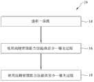
图1为实行本发明一个或数个实施例的微影方法;FIG. 1 is a lithography method for implementing one or several embodiments of the present invention;
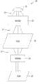
图2为实行本发明一个或数个实施例的微影系统;Fig. 2 is a lithography system implementing one or several embodiments of the present invention;
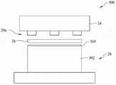
图3-6为实行本发明一个或数个实施例的微影系统的挑选构件;3-6 are selected components of a lithography system implementing one or more embodiments of the present invention;
图7a-7b为实行本发明一个或数个实施例的光阻图案;Figures 7a-7b are photoresist patterns implementing one or several embodiments of the present invention;
图8a至图8b为实行本发明一个或数个实施例的光阻图案;8a to 8b are photoresist patterns implementing one or several embodiments of the present invention;
图9为依照本发明一个或数个实施例的晶圆。FIG. 9 is a diagram of a wafer according to one or more embodiments of the present invention.
符号说明:Symbol Description:
10:微影方法 14:提供一晶圆10: Lithography method 14: Provide a wafer
16:使用高精密微影方法提供至少一曝光制程16: Provide at least one exposure process using high-precision lithography
18:使用低精密微影方法提供至少一曝光制程18: Provide at least one exposure process using low-precision lithography methods
20:微影系统 21:光源20: Lithography system 21: Light source
22:凝结器 23,25,27:光束22:
24,402:罩幕 24a,402a:铬层24,402:
26:投射镜 28,28’:晶圆26:
302,304a,304b,304c:光阻层 308:液体膜302, 304a, 304b, 304c: photoresist layer 308: liquid film
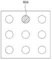
700,800:光阻图案 702:主动图案700,800: photoresist pattern 702: active pattern
704:虚设图案 804:预期图案704: False pattern 804: Expected pattern
910:基材 914:介电层910: Substrate 914: Dielectric layer
920:底部抗反光涂层920: bottom anti-reflective coating
具体实施方式Detailed ways
为更进一步阐述本发明为达成预定发明目的所采取的技术手段及功效,以下结合附图及较佳实施例,对依据本发明提出的半导体制造的微影方法其具体实施方式、制造方法、步骤、特征及其功效,详细说明如后。In order to further explain the technical means and effects of the present invention to achieve the intended purpose of the invention, the specific implementation, manufacturing method, and steps of the lithography method for semiconductor manufacturing proposed according to the present invention will be described below in conjunction with the accompanying drawings and preferred embodiments. , features and their effects are described in detail below.
请参阅图1所示,其为实行本发明一个或数个实施例的简化微影方法10。步骤14提供一晶圆。接着至步骤16,使用高精密微影方法(例如:湿浸式微影技术)提供至少一曝光制程至晶圆,随后至步骤18,使用低精密微影方法(例如:干式微影技术)提供一个或数个曝光制程至晶圆。Please refer to FIG. 1 , which is a
方法10可用于各种半导体元件的制造中,例如记忆体元件(包括但不限制在静态随机记忆体(SRAM))、逻辑元件(包括但不限制在金氧半场效晶体管(电晶体)(MOSFET)),及/或其他元件。方法10可特别应用在制造特征结构尺寸小于56nm的半导体元件中。方法10将配合图2-8进一步说明如下。
图2-6为示范一双重曝光制程,用以说明在第一曝光制程中使用一种较多增强型的技术,例如湿浸式微影技术;以及在第二曝光制程中使用一种较少增强型的技术,例如干式微影技术。Figures 2-6 illustrate a double exposure process, illustrating the use of a more enhanced technique, such as wet immersion lithography, in the first exposure process; and a less enhanced technique used in the second exposure process type of technology, such as dry lithography.
请特别参阅图2所示,为实行本发明一个或数个实施例的微影系统。一种简化示范的微影系统20包括一光源21,用以放射光束23使其经一凝结器22而凝结。光束27均匀地照射在具有图案的罩幕24上。在穿过罩幕之后,光束25会经投射镜26聚焦,然后才会投射在晶圆28上。Please refer in particular to FIG. 2 , which is a lithography system implementing one or several embodiments of the present invention. A simplified
双重曝光制程的第一曝光制程将进一步详细说明于下。请参阅图3所示,其为使用于图2的系统中的选择元件,包括晶圆28、投射镜26及罩幕24,晶圆28是在方法10的步骤14(图1)中提供。The first exposure process of the double exposure process will be further described in detail below. Please refer to FIG. 3 , which is an optional component used in the system of FIG. 2 , including a
在这个实施例中,晶圆28包括一光阻层302。光阻层302可以是经由旋涂式涂布及/或其他制程而被沉积于晶圆上。在本范例中,使用一光阻溶液施予晶圆28的表面上,然后快速旋转直到光阻溶液几乎干掉为止。在一范例中,光阻层302可以是使用酸性催化作用的一化学扩大式光阻。在此范例中,光阻层可经由将一酸性敏感聚合物溶解于一铸造溶液中而形成。In this embodiment,
投射镜26可包括熔融氧化硅(非结晶硅二氧化物)及/或现有已知任何其他适当的材料。The
罩幕24可以是含有电子电路显微图像的一高精密板。罩幕24可包括各种材料,例如石英、苏打石灰、白冠及/或其他材料。一般来说,罩幕24的一侧上可含有一铬层,而在铬层中(标号24a)可蚀刻出电子电路(通常称为几何线路)。在一范例中,罩幕24的厚度可以是介于大约60mm至大约250mm之间。
在一范例中,可在投射镜26与晶圆28之间插入一液体(未显示),以覆盖其的至少一部分。该液体可包括水、掺杂水(铬离子)、具pH值大于7的流体、具折射率大于1的流体,及/或其他物质。在一实施例中,液体膜308(可透过投射镜26的壳体的开口注射入)可覆盖晶圆28的暴露区。In one example, a liquid (not shown) may be interposed between the
依据方法10的步骤16,使用湿浸式微影技术进行晶圆28的第一曝光制程。在一范例中,湿浸式微影技术可包括光源(未显示),例如具波长不大于250nm的电磁源,及/或其他光源。在一实施例中,光源放射的光束波长是大约193nm、157nm及/或其他数字。可预期的是,光学系统的数值孔隙(NA)可大于大约0.75。According to step 16 of
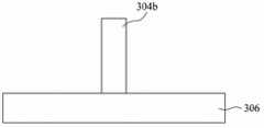
请参阅图4所示,在第一曝光制程之后,可使用真空装置(未显示)及/或其他适当方法移除液体膜308。之后,可使用现有已知的方法使光阻层302显影,以产生光阻结构304a、304b与304c。Referring to FIG. 4 , after the first exposure process, the
依据方法10的步骤18(在一些实施例中,其可在步骤16之前执行),使用干式微影技术进行晶圆28的第二曝光制程。According to step 18 of method 10 (which may be performed before
请参阅图5所示,其为一种微影系统的挑选构件,包括罩幕402与晶圆28’。再者,罩幕402可以是含有电子电路显微图像的一高精密板,并且可包括各种材料,例如石英、苏打石灰、白冠及/或其他材料。一般来说,罩幕402的一侧上可含有一铬层,而在铬层中(标号402a)可蚀刻出电子电路(通常称为几何线路)。Please refer to FIG. 5, which is a selected component of a lithography system, including a
第二曝光制程可使用干式微影技术来完成,其可包括现有已知的任何方法。干式微影技术的辐射波长可以是大约193nm、248nm及/或其他数字。需注意的是,在一些实施例中,可去除罩幕402,以进行一无罩幕曝光步骤。The second exposure process can be accomplished using dry lithography, which can include any known method. The wavelength of radiation for dry lithography may be approximately 193 nm, 248 nm, and/or other numbers. It should be noted that in some embodiments, the
在另一范例中,第一与第二曝光制程都是以具不同数值孔隙的湿浸式微影技术来完成。例如,当在一单晶片中暴露一高功率区与一低功率区时,可使用具大数值孔隙的第一湿浸式微影技术来曝光该高功率区,以及使用具小数值孔隙的第二湿浸式微影技术来曝光该低功率区。虽然制造成本较多,但是使用大数值孔隙来曝光高功率区将可获得较佳的图像解析度。另一方面,使用小数值孔隙来曝光低功率区将可降低制造成本。在一些实施例中,第一与第二湿浸式微影制程都是在相同的曝光机器中进行,例如步进机或扫描器,借以维持覆盖品质。在本发明中,高功率区中的线宽/间隔为等于或小于约0.25um,而低功率区中的线宽/间隔为大于约0.25um。In another example, both the first and second exposure processes are performed by wet immersion lithography with different numerical apertures. For example, when exposing a high power region and a low power region in a single wafer, the high power region can be exposed using a first immersion lithography technique with a large numerical aperture, and a second immersion lithography technique with a small numerical aperture can be used. Wet immersion lithography is used to expose the low power region. Although the manufacturing cost is higher, better image resolution can be obtained by using a large numerical aperture to expose the high power region. On the other hand, using small numerical apertures to expose low power regions will reduce manufacturing costs. In some embodiments, both the first and second immersion lithography processes are performed in the same exposure machine, such as a stepper or scanner, to maintain coverage quality. In the present invention, the line width/space in the high power region is equal to or less than about 0.25um, while the linewidth/space in the low power region is greater than about 0.25um.
请参阅图6所示,在第二曝光制程与显影之后,移除图5的光阻层304a与304c。Please refer to FIG. 6, after the second exposure process and development, the
需注意的是,在上述范例中,第一曝光制程可使用干式微影技术,而第二曝光制程可使用湿浸式微影技术。又需注意的是,关于上述范例,其他额外的曝光制程也可使用湿浸式微影技术及/或干式微影技术来完成。It should be noted that, in the above example, the first exposure process can use dry lithography, and the second exposure process can use immersion lithography. It should also be noted that, with respect to the above examples, other additional exposure processes can also be accomplished using immersion lithography and/or dry lithography.
需注意的是,本发明也可利用方法10来达到许多应用。在第二范例中,方法10可用在需要主动与虚设(dummy)图案的混合图案的制程中,例如一种使用相位移罩幕(垫制程(Pad Process))的孔洞印刷制程。该垫制程如Lin等人的美国专利第6,664,011号所描述,其说明书全部内容可并入此处做参考。It should be noted that the present invention can also use the
请参阅图7a所示,其为依照本发明一个或数个实施例的光阻图案700的上视图。在本实施例中,依据方法10的步骤16,首先,利用第一罩幕以193nm波长湿浸式微影技术对晶圆(图1)进行曝光,接着在光阻层(未显示)显影之后形成光阻图案700。在此图示中,主动图案702被虚设图案704所包围。虚设图案704可包括线端的虚设条或虚拟条,角缘圆化的虚拟条、虚设垫,及/或其他图案。Please refer to FIG. 7 a , which is a top view of a photoresist pattern 700 according to one or several embodiments of the present invention. In this embodiment, according to step 16 of the
请参阅图7b所示,依据方法10的步骤18,可透过第二曝光制程并利用248nm波长干式微影技术来去除虚设图案704。可预期的是,第二曝光制程可使用第二罩幕来达到。当然,第二曝光制程可以不使用任何罩幕来执行。在一范例中,干式微影制程的光源可包括一电磁源、一光束源及/或其他适当的来源。需注意的是,第二曝光制程也可使用湿浸式微影技术完成。Please refer to FIG. 7 b , according to step 18 of the
在第三范例中,方法10可应用在一隐蔽孔洞制程中。请参阅图8a,其为光阻图案800的一个示范上视图,是依据方法10的步骤16而形成,其是使用193nm波长湿浸式微影制程对晶圆曝光。在此图示中,光阻图案800缺少图案804(图8b所示)。依据方法10的步骤18,使用193nm波长干式微影制程对晶圆进行第二曝光制程。如熟悉技艺者所知,可执行一个或数个中间步骤(例如沉积一额外光阻层及/或其他步骤)。干式微影制程可包括使用罩幕或不使用罩幕的现有已知的任何方法,包括但不限制在电子束曝光方法。之后,在显影制程之后形成图8b的预期图案804。需注意的是,第二曝光制程也可使用湿浸式微影制程来完成。举例来说,第一曝光制程是193nm波长湿浸式微影制程,而第二曝光制程是248nm波长湿浸式微影制程。In a third example, the
此上述范例还可以有以下的各种变化。在一范例中,假如方法10是用于具主动与虚设图案的混合图案中,则主动图案的关键尺寸(CD)可包括一不大于90nm的线宽关键尺寸、一不大于120nm之间隔关键尺寸及/或一不大于120nm的孔洞关键尺寸。在另一范例中,方法10可应用在多重曝光制程,其包括单一光阻层或复数光阻层。在第三范例中,方法10可应用在多重曝光制程,其包括在多重曝光制程之后进行单一蚀刻制程。在第四范例中,可使用复数个蚀刻步骤,而任一蚀刻步骤可在单一曝光制程之后应用于晶圆上。在第五范例中,方法10可应用在各种制程中,例如线端缩短、移除至少一虚设闸极、修复缺掉的图案、减低密集与隔离图案之间不对等效应及/或其他制程。The above example can also have the following various changes. In one example, if the
请参阅图9所示,对于范例的目的,图3的晶圆28可展开而包括如图所示的基材910、介电层914及一底部抗反光涂层(以下称BARC层)920。Referring to FIG. 9, for exemplary purposes, the
基材910可包括一个或数个绝缘体、导体及/或半导体层。举例来说,基材910可包括一元素半导体,例如结晶硅、多晶硅、非晶硅及/或锗;一化合物半导体,例如碳化硅及/或砷化镓;一合金半导体,例如SiGe、GaAsP、AlInAs、AlGaAs及/或GaInP。此外,基材910可包括一主体半导体,例如主体硅,以及一主体半导体可包括磊晶硅层。其也可包括一绝缘层上覆半导体基材,例如绝缘层上覆硅(SOI)基材,或一薄膜晶体管(电晶体)(TFT)基材。基材910也可包括一多硅基材或一多层化合物半导体基材。
介电层914可沉积于基材910的表面上。介电层914可由CVD、PECVD、ALD、PVD、旋涂式涂布法及/或其他制程来形成。介电层914可以是内金属介电层(IMD),且其可包括低介电(low-k)材料、二氧化硅、聚硫亚氨、旋涂式玻璃(SOG)、氟化硅玻璃(FSG)、黑钻石(Black Diamond,美商应用材料的产品名称及商标)、干凝胶、气凝胶、氟化非晶碳及/或其他材料。A
可使用各种技术沉积BARC层920于介电层914上,包括但不限制在旋涂式涂布法、PVD、CVD及/或其他制程。The
在一范例中,BARC层920可吸收不慎穿过光阻层底部(未显示)的光线。为了执行光吸收,BARC层920可包括具有高消灭系数的材料及/或相当大的厚度。另一方面,BARC层920的高系数可导致BARC层的高反射比,其将会抵消BARC层920的有效性。因此,可得知BARC层920可拥有大概介于大约0.2至大约0.5之间的系数值,并且可拥有大约200nm的厚度。然而,需注意的是,本发明也可以是其他范围的系数值与厚度。In one example, the
此外,一种索引相称方法(index matching approach)也可应用于BARC层920中。在这种方法下,BARC层920可包括具有符合光的一折射索引与厚度的材料。在操作时,一旦光照在BARC层920时,一部分光将会被反射。同时,另一部分光会进入BARC层920,并被转换成具有相位移之光,其将会干涉到从BARC层920反射之光的第一部分,因而造成光反射比降低。In addition, an index matching approach can also be applied in the
可预期的是,BARC层920可同时使用光吸收与索引相称方法,借以达到预期结果。在一些例子中,若要移除BARC层920可能较难以达到,则BARC层920可仅遗留在介电层914上,以做为晶圆18的扩散阻障层。It is contemplated that the
在沉积光阻层之后,晶圆28可经过软烤步骤及双曝光制程(如以上方法10所述)。After depositing the photoresist layer,
随后,可使用额外的步骤,以形成一个完整的半导体元件。这些额外的步骤如熟悉此技艺者所知,此处不再赘述。Subsequently, additional steps may be used to form a complete semiconductor element. These additional steps are known to those skilled in the art and will not be repeated here.
以上所述,仅是本发明的较佳实施例而已,并非对本发明作任何形式上的限制,虽然本发明已以较佳实施例揭露如上,然而并非用以限定本发明,任何熟悉本专业的技术人员,在不脱离本发明技术方案范围内,当可利用上述揭示的技术内容作出些许更动或修饰为等同变化的等效实施例,但凡是未脱离本发明技术方案内容,依据本发明的技术实质对以上实施例所作的任何简单修改、等同变化与修饰,均仍属于本发明技术方案的范围内。The above description is only a preferred embodiment of the present invention, and does not limit the present invention in any form. Although the present invention has been disclosed as above with preferred embodiments, it is not intended to limit the present invention. Anyone familiar with this field Those skilled in the art, without departing from the scope of the technical solution of the present invention, may use the technical content disclosed above to make some changes or modify equivalent embodiments with equivalent changes, but if they do not depart from the content of the technical solution of the present invention, according to the Technical Essence Any simple modifications, equivalent changes and modifications made to the above embodiments still fall within the scope of the technical solution of the present invention.
Claims (20)
Applications Claiming Priority (2)
| Application Number | Priority Date | Filing Date | Title |
|---|---|---|---|
| US11/216,658US7501227B2 (en) | 2005-08-31 | 2005-08-31 | System and method for photolithography in semiconductor manufacturing |
| US11/216,658 | 2005-08-31 |
Related Parent Applications (1)
| Application Number | Title | Priority Date | Filing Date |
|---|---|---|---|
| CNA2006101121367ADivisionCN1924706A (en) | 2005-08-31 | 2006-08-11 | Lithography Methods for Semiconductor Manufacturing |
Publications (1)
| Publication Number | Publication Date |
|---|---|
| CN103345120Atrue CN103345120A (en) | 2013-10-09 |
Family
ID=36698816
Family Applications (2)
| Application Number | Title | Priority Date | Filing Date |
|---|---|---|---|
| CN2013102258795APendingCN103345120A (en) | 2005-08-31 | 2006-08-11 | Lithographic method of semiconductor manufacture |
| CNA2006101121367APendingCN1924706A (en) | 2005-08-31 | 2006-08-11 | Lithography Methods for Semiconductor Manufacturing |
Family Applications After (1)
| Application Number | Title | Priority Date | Filing Date |
|---|---|---|---|
| CNA2006101121367APendingCN1924706A (en) | 2005-08-31 | 2006-08-11 | Lithography Methods for Semiconductor Manufacturing |
Country Status (10)
| Country | Link |
|---|---|
| US (2) | US7501227B2 (en) |
| JP (1) | JP2007067376A (en) |
| KR (1) | KR100747625B1 (en) |
| CN (2) | CN103345120A (en) |
| DE (2) | DE102006015722B4 (en) |
| FR (1) | FR2891066B1 (en) |
| IL (1) | IL174923A (en) |
| NL (1) | NL2000103C2 (en) |
| SG (1) | SG130083A1 (en) |
| TW (1) | TWI311339B (en) |
Cited By (1)
| Publication number | Priority date | Publication date | Assignee | Title |
|---|---|---|---|---|
| CN110231725A (en)* | 2019-05-20 | 2019-09-13 | 深圳市华星光电半导体显示技术有限公司 | A kind of method and its control system of the thinning of lithographic glass |
Families Citing this family (14)
| Publication number | Priority date | Publication date | Assignee | Title |
|---|---|---|---|---|
| US7501227B2 (en)* | 2005-08-31 | 2009-03-10 | Taiwan Semiconductor Manufacturing Company | System and method for photolithography in semiconductor manufacturing |
| JP4837971B2 (en)* | 2005-10-07 | 2011-12-14 | ルネサスエレクトロニクス株式会社 | Manufacturing method of semiconductor device |
| US7803516B2 (en)* | 2005-11-21 | 2010-09-28 | Nikon Corporation | Exposure method, device manufacturing method using the same, exposure apparatus, and substrate processing method and apparatus |
| KR100827506B1 (en)* | 2006-05-11 | 2008-05-06 | 주식회사 하이닉스반도체 | Method of manufacturing semiconductor device using immersion lithography process |
| US8346872B2 (en)* | 2006-06-30 | 2013-01-01 | The Invention Science Fund I, Llc | Context parameters and identifiers for communication |
| JP4357514B2 (en)* | 2006-09-29 | 2009-11-04 | 株式会社東芝 | Immersion exposure method |
| US8139199B2 (en)* | 2007-04-02 | 2012-03-20 | Nikon Corporation | Exposure method, exposure apparatus, light converging pattern formation member, mask, and device manufacturing method |
| KR100961204B1 (en) | 2008-06-18 | 2010-06-09 | 주식회사 하이닉스반도체 | Pattern formation method of semiconductor device using mixed auxiliary pattern |
| US8728722B2 (en)* | 2010-09-30 | 2014-05-20 | Truesense Imaging, Inc. | Stitching methods using multiple microlithographic expose tools |
| US8728945B2 (en)* | 2010-11-03 | 2014-05-20 | Texas Instruments Incorporated | Method for patterning sublithographic features |
| KR20140029050A (en)* | 2012-08-31 | 2014-03-10 | 삼성전자주식회사 | Method of forming pattern |
| US9097975B2 (en) | 2012-09-14 | 2015-08-04 | Macronix International Co., Ltd. | Double patterning by PTD and NTD process |
| US8835100B2 (en)* | 2012-09-14 | 2014-09-16 | Macronix International Co., Ltd. | Double patterning by PTD and NTD process |
| US9274413B2 (en) | 2013-09-11 | 2016-03-01 | United Microelectronics Corp. | Method for forming layout pattern |
Family Cites Families (27)
| Publication number | Priority date | Publication date | Assignee | Title |
|---|---|---|---|---|
| JPH0582414A (en)* | 1991-09-24 | 1993-04-02 | Nec Kyushu Ltd | Reduced projection exposure |
| WO1994024610A1 (en) | 1993-04-13 | 1994-10-27 | Astarix, Inc. | High resolution mask programmable via selected by low resolution photomasking |
| JP3015224B2 (en)* | 1993-05-26 | 2000-03-06 | キヤノン株式会社 | Exposure method |
| JP2993320B2 (en)* | 1993-05-27 | 1999-12-20 | キヤノン株式会社 | Exposure apparatus and method for manufacturing semiconductor device using the same |
| JPH07211619A (en)* | 1994-01-25 | 1995-08-11 | Hitachi Ltd | Method of forming circuit pattern and reticle used therefor |
| JP3492846B2 (en)* | 1996-04-26 | 2004-02-03 | 株式会社東芝 | Method for manufacturing semiconductor device |
| JPH11133585A (en)* | 1997-10-30 | 1999-05-21 | Nec Corp | Mask for exposure and its production |
| US6080533A (en)* | 1998-03-10 | 2000-06-27 | Clear Logic, Inc. | Method of patterning photoresist using precision and non-precision techniques |
| JPH11327121A (en) | 1998-05-20 | 1999-11-26 | Toppan Printing Co Ltd | Manufacturing method of halftone type phase shift mask and blank of halftone type phase shift mask |
| JP2000021749A (en)* | 1998-06-30 | 2000-01-21 | Canon Inc | Exposure method and exposure apparatus |
| US6664011B2 (en) | 2001-12-05 | 2003-12-16 | Taiwan Semiconductor Manufacturing Company | Hole printing by packing and unpacking using alternating phase-shifting masks |
| US6839126B2 (en)* | 2002-01-03 | 2005-01-04 | United Microelectronics Corp. | Photolithography process with multiple exposures |
| US6894762B1 (en) | 2002-09-17 | 2005-05-17 | Lsi Logic Corporation | Dual source lithography for direct write application |
| KR100523839B1 (en)* | 2002-10-07 | 2005-10-27 | 한국전자통신연구원 | Dry lithography process and method of forming gate pattern using the same |
| US6788477B2 (en)* | 2002-10-22 | 2004-09-07 | Taiwan Semiconductor Manufacturing Co., Ltd. | Apparatus for method for immersion lithography |
| DE10258718A1 (en) | 2002-12-09 | 2004-06-24 | Carl Zeiss Smt Ag | Projection lens, in particular for microlithography, and method for tuning a projection lens |
| WO2004053955A1 (en)* | 2002-12-10 | 2004-06-24 | Nikon Corporation | Exposure system and device producing method |
| JP2004294977A (en)* | 2003-03-28 | 2004-10-21 | Nikon Corp | Pattern production method and pattern production system, mask production method and mask production system, mask, exposure method and exposure apparatus, and device production method |
| JP4305095B2 (en) | 2003-08-29 | 2009-07-29 | 株式会社ニコン | Immersion projection exposure apparatus equipped with an optical component cleaning mechanism and immersion optical component cleaning method |
| JP2005136374A (en) | 2003-10-06 | 2005-05-26 | Matsushita Electric Ind Co Ltd | Semiconductor manufacturing apparatus and pattern forming method using the same |
| JP4540327B2 (en)* | 2003-11-06 | 2010-09-08 | ルネサスエレクトロニクス株式会社 | Photomask pattern forming method |
| JP2005191381A (en)* | 2003-12-26 | 2005-07-14 | Canon Inc | Exposure method and apparatus |
| US20050147920A1 (en) | 2003-12-30 | 2005-07-07 | Chia-Hui Lin | Method and system for immersion lithography |
| WO2005076084A1 (en) | 2004-02-09 | 2005-08-18 | Carl Zeiss Smt Ag | Projection objective for a microlithographic projection exposure apparatus |
| JP4625673B2 (en)* | 2004-10-15 | 2011-02-02 | 株式会社東芝 | Exposure method and exposure apparatus |
| JP3976046B2 (en)* | 2004-11-11 | 2007-09-12 | ソニー株式会社 | Exposure apparatus, semiconductor device manufacturing apparatus, phase shift mask, and design method |
| US7501227B2 (en)* | 2005-08-31 | 2009-03-10 | Taiwan Semiconductor Manufacturing Company | System and method for photolithography in semiconductor manufacturing |
- 2005
- 2005-08-31USUS11/216,658patent/US7501227B2/enactiveActive
- 2006
- 2006-03-07SGSG200601548-1Apatent/SG130083A1/enunknown
- 2006-04-04DEDE102006015722.2Apatent/DE102006015722B4/enactiveActive
- 2006-04-04DEDE102006062993.0Apatent/DE102006062993B3/enactiveActive
- 2006-04-11ILIL174923Apatent/IL174923A/enactiveIP Right Grant
- 2006-05-18TWTW095117711Apatent/TWI311339B/ennot_activeIP Right Cessation
- 2006-05-29KRKR1020060048012Apatent/KR100747625B1/enactiveActive
- 2006-06-15NLNL2000103Apatent/NL2000103C2/enactiveSearch and Examination
- 2006-06-27FRFR0605792Apatent/FR2891066B1/enactiveActive
- 2006-07-03JPJP2006183322Apatent/JP2007067376A/enactivePending
- 2006-08-11CNCN2013102258795Apatent/CN103345120A/enactivePending
- 2006-08-11CNCNA2006101121367Apatent/CN1924706A/enactivePending
- 2009
- 2009-01-29USUS12/362,316patent/US8178289B2/ennot_activeExpired - Fee Related
Cited By (2)
| Publication number | Priority date | Publication date | Assignee | Title |
|---|---|---|---|---|
| CN110231725A (en)* | 2019-05-20 | 2019-09-13 | 深圳市华星光电半导体显示技术有限公司 | A kind of method and its control system of the thinning of lithographic glass |
| CN110231725B (en)* | 2019-05-20 | 2022-03-08 | 深圳市华星光电半导体显示技术有限公司 | Method for thinning micro-image glass and control system thereof |
Also Published As
| Publication number | Publication date |
|---|---|
| US7501227B2 (en) | 2009-03-10 |
| NL2000103C2 (en) | 2007-08-07 |
| TW200709276A (en) | 2007-03-01 |
| NL2000103A1 (en) | 2007-03-01 |
| US8178289B2 (en) | 2012-05-15 |
| DE102006015722B4 (en) | 2020-05-14 |
| IL174923A (en) | 2011-06-30 |
| TWI311339B (en) | 2009-06-21 |
| CN1924706A (en) | 2007-03-07 |
| FR2891066A1 (en) | 2007-03-23 |
| US20090136876A1 (en) | 2009-05-28 |
| KR20070025954A (en) | 2007-03-08 |
| KR100747625B1 (en) | 2007-08-08 |
| DE102006062993B3 (en) | 2021-03-11 |
| FR2891066B1 (en) | 2018-02-02 |
| DE102006015722A1 (en) | 2007-03-22 |
| US20070048678A1 (en) | 2007-03-01 |
| SG130083A1 (en) | 2007-03-20 |
| IL174923A0 (en) | 2006-10-05 |
| JP2007067376A (en) | 2007-03-15 |
Similar Documents
| Publication | Publication Date | Title |
|---|---|---|
| CN103345120A (en) | Lithographic method of semiconductor manufacture | |
| US20080292991A1 (en) | High fidelity multiple resist patterning | |
| JP2004134553A (en) | Process for forming resist pattern and process for fabricating semiconductor device | |
| US20050069788A1 (en) | Photomask, photomask manufacturing method and semiconductor device manufacturing method using photomask | |
| US7838173B2 (en) | Structure design and fabrication on photomask for contact hole manufacturing process window enhancement | |
| US8637214B2 (en) | Photomask sets for fabricating semiconductor devices | |
| US20100073648A1 (en) | Masks and Methods of Manufacture Thereof | |
| KR100549319B1 (en) | Chromium-free alternating reticles for fabricating semiconductor device features | |
| JP2001291651A (en) | Method for forming resist pattern, and method for manufacturing semiconductor device | |
| WO2002043139A2 (en) | Two mask via pattern to improve pattern definition | |
| US8003302B2 (en) | Method for fabricating patterns using a photomask | |
| US10274817B2 (en) | Mask and photolithography system | |
| KR20030056499A (en) | Mask for Forming Minute Pattern | |
| KR100846678B1 (en) | A system and method for photolithography in semiconductor manufacturing | |
| JP2000021978A (en) | Photomask and pattern forming method | |
| KR20090103629A (en) | EUV mask and manufacturing method the same | |
| US20050031966A1 (en) | Method to improve photomask critical dimension uniformity and photomask fabrication process | |
| JP3422054B2 (en) | Optical mask and method of manufacturing the same | |
| US8242021B2 (en) | Method for manufacturing semiconductor device | |
| JP2693805B2 (en) | Reticle and pattern forming method using the same | |
| JP4225544B2 (en) | Laminated structure of photosensitive material and method for forming fine pattern | |
| JPH10312994A (en) | Manufacture of semiconductor device | |
| JP2002072444A (en) | Method for manufacturing semiconductor integrated circuit device | |
| JP3225673B2 (en) | Method for manufacturing phase shift mask | |
| KR100401517B1 (en) | Method of fabricating exposure mask for semiconductor manufacture |
Legal Events
| Date | Code | Title | Description |
|---|---|---|---|
| C06 | Publication | ||
| PB01 | Publication | ||
| C10 | Entry into substantive examination | ||
| SE01 | Entry into force of request for substantive examination | ||
| RJ01 | Rejection of invention patent application after publication | Application publication date:20131009 | |
| RJ01 | Rejection of invention patent application after publication |