CN103326596A - Power Supply Circuit and AC Signal Rectification Method - Google Patents
Power Supply Circuit and AC Signal Rectification MethodDownload PDFInfo
- Publication number
- CN103326596A CN103326596ACN2012100775260ACN201210077526ACN103326596ACN 103326596 ACN103326596 ACN 103326596ACN 2012100775260 ACN2012100775260 ACN 2012100775260ACN 201210077526 ACN201210077526 ACN 201210077526ACN 103326596 ACN103326596 ACN 103326596A
- Authority
- CN
- China
- Prior art keywords
- signal
- switch
- circuit
- line
- neutral
- Prior art date
- Legal status (The legal status is an assumption and is not a legal conclusion. Google has not performed a legal analysis and makes no representation as to the accuracy of the status listed.)
- Granted
Links
Images


Landscapes
- Rectifiers (AREA)
Abstract
Description
Translated fromChinese技术领域technical field
本发明涉及一种电源供应电路及交流讯号整流方法,特别是指一种改善整流效率并节省电力的电源供应电路及交流讯号整流方法。The invention relates to a power supply circuit and an AC signal rectification method, in particular to a power supply circuit and an AC signal rectification method which improve rectification efficiency and save power.
背景技术Background technique
图1显示一种典型的桥式整流电源供应电路100,其中,桥式整流电路11包含一对逆向端互相耦接的二极管与一对顺向端互相耦接的二极管,并接于交流讯号AC之间,以将交流讯号AC转换为整流讯号Vol。这种典型的桥式整流电源供应电路100提供交流讯号AC的全波整流(full-wave rectification),但由于二极管具有顺向压降(forwardvoltage drop),对许多应用来说,相较于输出电压,此顺向压降不可被忽略,因此造成整流效率的下降。此外,在高频的切换式电源供应电路中,二极管的热消散(heat dissipation)问题,亦会降低整流效率,且造成电路可靠度的问题。FIG. 1 shows a typical bridge rectification
请参阅图2,显示美国专利US7,411,768所揭示的电源供应电路200。如图所示,电源供应电路200将交流讯号AC整流后转换为整流讯号Vo2。相较于前述典型桥式整流电源供应电路100,电源供应电路200虽然可以改善整流效率以及热消散问题;但其利用金属氧化物半导体(metal oxide semiconductor,MOS)元件与肖特基二极管元件的物理特性,无法精确控制开关导通的时间点,仍有整流效率的问题;且这种整流的方式,无法达成省电的模式控制。Please refer to FIG. 2 , which shows a
此外,上述现有技术中,尚包含其它的缺点,例如:温度的变化往往影响其元件的操作;精确度较差;去除噪声能力较弱;无法根据需求调整;无法达成省电模式;其侦测交流讯号的电路的RC值较低,容易造成元件贯穿(shoot through)等等。In addition, the above-mentioned prior art still contains other disadvantages, for example: the change of temperature often affects the operation of its components; the accuracy is poor; the ability to remove noise is weak; The RC value of the circuit for measuring AC signals is low, which is easy to cause component shoot through and so on.
有鉴于此,本发明即针对上述现有技术的不足,提出一种电源供应电路及交流讯号整流方法,可改善整流效率并节省电力。In view of this, the present invention aims at the shortcomings of the above-mentioned prior art, and proposes a power supply circuit and an AC signal rectification method, which can improve rectification efficiency and save power.
发明内容Contents of the invention
本发明目的之一在于克服现有技术的不足与缺陷,提出一种电源供应电路。One of the objectives of the present invention is to overcome the deficiencies and defects of the prior art and provide a power supply circuit.
本发明另一目的在于,提出一种交流讯号整流方法。Another object of the present invention is to provide an AC signal rectification method.
为达上述目的,就其中一观点言,本发明提供了一种电源供应电路,用以将一交流讯号转换为一整流讯号,该交流讯号包括一线位(line)讯号与一中位(neutral)讯号,该电源供应电路包含:一桥式整流电路,包括一对逆向端互相耦接的二极管与一对互相耦接的开关元件,该对二极管与该对开关元件并接于该线位讯号与该中位讯号之间,该桥式整流电路根据至少一开关操作讯号,操作该对开关元件,以转换该交流讯号为该整流讯号;以及一控制电路,根据该交流讯号,产生该开关操作讯号,以操作该对开关元件;其中,该对开关元件包括一第一开关与一第二开关,该第一开关耦接于该线位讯号,且该第二开关耦接于该中位讯号,当该线位讯号高于该中位讯号一第一默认值时,导通该第二开关,当该中位讯号高于该线位讯号一第二默认值时,导通该第一开关。该第一默认值与该第二默认值可以相同或不同。In order to achieve the above purpose, from one point of view, the present invention provides a power supply circuit for converting an AC signal into a rectified signal, the AC signal includes a line signal and a neutral (neutral) signal, the power supply circuit includes: a bridge rectifier circuit, including a pair of diodes with opposite ends coupled to each other and a pair of switching elements coupled to each other, the pair of diodes and the pair of switching elements are connected in parallel between the line signal and Between the neutral signal, the bridge rectifier circuit operates the pair of switch elements according to at least one switch operation signal to convert the AC signal into the rectified signal; and a control circuit generates the switch operation signal according to the AC signal , to operate the pair of switching elements; wherein, the pair of switching elements includes a first switch and a second switch, the first switch is coupled to the line signal, and the second switch is coupled to the neutral signal, When the line signal is higher than a first default value of the neutral signal, the second switch is turned on; when the middle signal is higher than a second default value of the line signal, the first switch is turned on. The first default value and the second default value may be the same or different.
就另一观点,本发明也提供了一种交流讯号整流方法,用以将一交流讯号转换为一整流讯号,该交流讯号包括一线位(line)讯号与一中位(neutral)讯号,该交流讯号整流方法包含:提供一桥式整流电路,其包括一对逆向端互相耦接的二极管与一对互相耦接的开关元件,该对二极管与该对开关元件并接于该线位讯号与该中位讯号之间,其中该对开关元件包括一第一开关与一第二开关,该第一开关耦接于该线位讯号,且该第二开关耦接于该中位讯号;当该线位讯号高于该中位讯号一第一默认值时,导通该第二开关;以及当该中位讯号高于该线位讯号一第二默认值时,导通该第一开关,通过此,将该交流讯号转换为该整流讯号。该第一默认值与该第二默认值可以相同或不同。From another point of view, the present invention also provides an AC signal rectification method for converting an AC signal into a rectified signal. The AC signal includes a line signal and a neutral signal. The AC signal The signal rectification method includes: providing a bridge rectification circuit, which includes a pair of diodes with opposite ends coupled to each other and a pair of switching elements coupled to each other, the pair of diodes and the pair of switching elements are connected in parallel between the line signal and the Between the neutral signal, wherein the pair of switching elements includes a first switch and a second switch, the first switch is coupled to the line signal, and the second switch is coupled to the neutral signal; when the line When the bit signal is higher than the first default value of the neutral signal, the second switch is turned on; and when the middle signal is higher than the line bit signal, a second default value, the first switch is turned on, through , converting the AC signal into the rectified signal. The first default value and the second default value may be the same or different.
在其中一种实施型态中,其中该控制电路宜包括:一第一比较电路,比较相关于该线位讯号的一第一讯号与相关于该中位讯号的一第二讯号,并根据比较结果,产生一第二开关控制讯号以控制该第二开关;以及一第二比较电路,比较该第二讯号与该第一讯号,并根据比较结果,产生一第一开关控制讯号以控制该第一开关。In one of the implementation forms, the control circuit preferably includes: a first comparison circuit, which compares a first signal related to the line bit signal with a second signal related to the median signal, and according to the comparison As a result, a second switch control signal is generated to control the second switch; and a second comparison circuit compares the second signal with the first signal, and generates a first switch control signal to control the first switch according to the comparison result a switch.
上述电源供应电路中,控制电路宜更包括一轻载侦测电路,具有:一第三比较电路,比较一第三参考讯号与该第二讯号,并根据比较结果,产生一第一侦测讯号;一第四比较电路,比较该第三参考讯号与该第一讯号,并根据比较结果,产生一第二侦测讯号;一第一逻辑电路,根据该第一侦测讯号与该第二开关控制讯号,决定该第二开关导通或不导通;以及一第二逻辑电路,根据该第二侦测讯号与该第一开关控制讯号,决定该第一开关导通或不导通。In the above power supply circuit, the control circuit preferably further includes a light load detection circuit, which has: a third comparison circuit, which compares a third reference signal with the second signal, and generates a first detection signal according to the comparison result ; A fourth comparison circuit, which compares the third reference signal with the first signal, and generates a second detection signal according to the comparison result; a first logic circuit, which generates a second detection signal according to the first detection signal and the second switch A control signal determines whether the second switch is turned on or not; and a second logic circuit determines whether the first switch is turned on or not according to the second detection signal and the first switch control signal.
在另一种实施型态中,控制电路宜更包括一去突波电路与一操作电路,其中该去突波电路与该第一比较电路与该第二比较电路耦接,以对该第一比较电路与该第二比较电路的比较结果,进行去突波处理;且该操作电路根据该第一比较电路与该第二比较电路的比较结果,产生该开关操作讯号以操作该第一开关与该第二开关。In another implementation mode, the control circuit preferably further includes a surge removal circuit and an operation circuit, wherein the surge removal circuit is coupled to the first comparison circuit and the second comparison circuit to control the first The comparison result of the comparison circuit and the second comparison circuit is subjected to deglitch processing; and the operation circuit generates the switch operation signal to operate the first switch and the second comparison circuit according to the comparison result of the first comparison circuit and the second comparison circuit. the second switch.
在另一种实施型态中,电源供应电路宜更包含一分压电路,以将该线位讯号与该中位讯号分别转换为该第一讯号与该第二讯号,使得该第一讯号与该第二讯号分别正比于该线位讯号与该中位讯号。In another implementation mode, the power supply circuit preferably further includes a voltage divider circuit to convert the line signal and the neutral signal into the first signal and the second signal respectively, so that the first signal and the The second signal is respectively proportional to the line signal and the median signal.
下面通过具体实施例详加说明,当更容易了解本发明的目的、技术内容、特点及其所达成的功效。The following will be described in detail through specific embodiments, so that it is easier to understand the purpose, technical content, characteristics and effects of the present invention.
附图说明Description of drawings
图1显示一种典型的桥式整流电源供应电路;Figure 1 shows a typical bridge rectifier power supply circuit;
图2显示美国专利US7,411,768所揭示的电源供应电路;Figure 2 shows the power supply circuit disclosed in US Patent No. 7,411,768;
图3显示本发明第一个实施例;Fig. 3 shows the first embodiment of the present invention;
图4显示线位讯号L、中位讯号N、开关操作讯号G1与G2的讯号波形;FIG. 4 shows the signal waveforms of the line position signal L, the neutral position signal N, and the switch operation signals G1 and G2;
图5显示本发明第二个实施例;Fig. 5 shows the second embodiment of the present invention;
图6显示本发明第三个实施例;Fig. 6 shows the third embodiment of the present invention;
图7显示本发明第四个实施例;Fig. 7 shows the fourth embodiment of the present invention;
图8显示本发明第五个实施例;Fig. 8 shows the fifth embodiment of the present invention;
图9A-9B显示本发明第六个实施例;9A-9B show a sixth embodiment of the present invention;
图10A-10B显示负载电路分别为重载与轻载时的线位讯号L、中位讯号N、与虚接地FGND的讯号波形图;10A-10B show the signal waveform diagrams of the line signal L, the neutral signal N, and the virtual ground FGND when the load circuit is heavy load and light load respectively;
图11A-11B显示负载电路分别为重载与轻载时的线位讯号L、中位讯号N、虚接地FGND、与开关操作讯号G1与G2的讯号波形图;11A-11B show the signal waveform diagrams of the line signal L, the neutral signal N, the virtual ground FGND, and the switch operation signals G1 and G2 when the load circuit is heavy load and light load respectively;
图12显示应用本发明的电路示意图;Fig. 12 shows the schematic circuit diagram of applying the present invention;
图13显示本发明在不同应用情况下,电力节省比例的示意图。FIG. 13 shows a schematic diagram of power saving ratios of the present invention under different application conditions.
图中符号说明Explanation of symbols in the figure
31 桥式整流电路31 Bridge rectifier circuit
33,43,53 控制电路33, 43, 53 control circuit
100,200,300 电源供应电路100, 200, 300 Power supply circuit
331,332,433,434 比较电路331, 332, 433, 434 comparison circuit
338,339 分压电路338, 339 Voltage divider circuit
435 轻载侦测电路435 Light load detection circuit
536,537 电路536, 537 Circuits
AC 交流讯号AC AC signal
AND1,AND2 门电路AND1, AND2 gate circuit
App1-4 应用一~四App1-4 Application one to four
D1,D2 二极管D1, D2 diodes
Div1,Div2 讯号Div1, Div2 signal
FGND 虚接地FGND virtual ground
G1,G2 开关操作讯号G1, G2 switch operation signal
G11,G21 开关控制讯号G11, G21 switch control signal
Id 电流Id Current
L 线位讯号L Line bit signal
N 中位讯号N median signal
Q1,Q2 开关元件Q1, Q2 switching elements
Vo1,Vo2,Vo3 整流讯号Vo1, Vo2, Vo3 rectified signal
Vref1,Vref2 默认值Vref1, Vref2 default value
Vref3,Vref4 参考讯号Vref3, Vref4 Reference signal
具体实施方式Detailed ways
请参阅图3,显示本发明第一个实施例,以说明本发明的基本概念。电源供应电路300包含桥式整流电路31以及控制电路33。桥式整流电路31将交流讯号AC转换为整流讯号Vo3,其中,交流讯号AC包含线位讯号L与中位讯号N,线位讯号L与中位讯号N的讯号波形如图4上方所示,其例如为相位相差180度的两正弦波。桥式整流电路31包括一对逆向端互相耦接的二极管D1与D2;与一对互相耦接的开关元件Q1与Q2。二极管对D1与D2与开关元件对Q1与Q2并接于线位讯号L与中位讯号N之间。控制电路33根据交流讯号AC,产生开关操作讯号G1与G2,分别操作开关元件Q1与Q2,以转换交流讯号AC为整流讯号Vo3。Please refer to FIG. 3, which shows the first embodiment of the present invention to illustrate the basic concept of the present invention. The
其中,开关元件Q1耦接于线位讯号L,且开关元件Q2耦接于中位讯号N。请参阅图4,除显示线位讯号L与中位讯号N之外,并显示开关操作讯号G1与G2的讯号波形。当线位讯号L高于中位讯号N加上默认值Vref1时,控制电路33产生的开关操作讯号G2例如由低位准转为高位准,以导通开关元件Q2;而当中位讯号N高于线位讯号L加上默认值Vref1时,开关操作讯号G1例如由低位准转为高位准,以导通开关元件Q1。Wherein, the switch element Q1 is coupled to the line signal L, and the switch element Q2 is coupled to the neutral signal N. Please refer to FIG. 4 , which shows the signal waveforms of the switch operation signals G1 and G2 in addition to the line signal L and the neutral signal N. When the line signal L is higher than the neutral signal N plus the default value Vref1, the switch operation signal G2 generated by the
与典型的桥式整流电路相较之下,第一个实施例利用开关元件Q1与Q2取代两二极管,以避免二极管导通时的顺向电压过高,并且提高桥式整流电路31的效率。此外,默认值Vref1用以确保开关元件Q1与Q2不会同时导通,以避免造成造成元件贯穿(shoot through)的问题。Compared with the typical bridge rectifier circuit, the first embodiment uses switching elements Q1 and Q2 instead of two diodes to avoid excessive forward voltage when the diodes are turned on and improve the efficiency of the
与图2所显示的现有技术相比,本实施例可精确控制开关元件Q1与Q2导通的时间点,而进一步增加整流效率;且利用本发明的整流方式,可以达成省电的模式控制。此外,本发明尚包含其它优于上述现有技术之处,例如:本发明可以避免温度的变化所造成的影响;可设计去噪声电路,以降低噪声的影响;并可根据应用需求调整;侦测交流讯号的电路,可利用比较电路提高RC值,进一步确保避免造成元件贯穿等等。Compared with the prior art shown in FIG. 2 , this embodiment can precisely control the time point at which the switching elements Q1 and Q2 are turned on, thereby further increasing the rectification efficiency; and using the rectification method of the present invention, power-saving mode control can be achieved . In addition, the present invention still includes other advantages over the above-mentioned prior art, for example: the present invention can avoid the influence caused by the change of temperature; the denoising circuit can be designed to reduce the influence of noise; and it can be adjusted according to application requirements; For circuits measuring AC signals, the comparison circuit can be used to increase the RC value to further ensure that components are not penetrated and so on.
图5显示本发明第二个实施例。与第一个实施例不同的是,如图5所示,开关操作讯号G1与开关操作讯号G2保持在高位准的时间不同,也就是说,本发明可以根据需要,设置不同的默认值Vref1与Vref2,以使开关操作讯号G1与开关操作讯号G2保持在高位准的时间不同。如图所示,当线位讯号L高于中位讯号N加上默认值Vref1时,控制电路33产生的开关操作讯号G2例如由低位准转为高位准,以导通开关元件Q2;而当中位讯号N高于线位讯号L加上默认值Vref2时,开关操作讯号G1例如由低位准转为高位准,以导通开关元件Q1。Fig. 5 shows a second embodiment of the present invention. The difference from the first embodiment is that, as shown in FIG. 5 , the switch operation signal G1 and the switch operation signal G2 are kept at a high level at different times. That is to say, the present invention can set different default values Vref1 and Vref1 as required. Vref2 , so that the switching operation signal G1 and the switching operation signal G2 are kept at a high level at different times. As shown in the figure, when the line level signal L is higher than the neutral level signal N plus the default value Vref1, the switching operation signal G2 generated by the
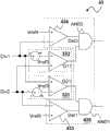
图6显示本发明第三个实施例。本实施例为控制电路33一个较具体的实施例。如图所示,控制电路33包含比较电路331与332。讯号Div1相关于线位讯号L,例如为线位讯号L的分压;讯号Div2相关于中位讯号N,例如为中位讯号N的分压。比较电路331比较讯号Div1与讯号Div2,并根据比较结果,产生开关控制讯号G21以控制开关元件Q2,例如但不限于如图所示,当讯号Div1高于讯号Div2加上参考讯号Vref3时,开关控制讯号G21例如由低位准转为高位准。开关控制讯号G21例如可通过具有适当驱动力的驱动闸而产生开关操作讯号G2,以操作开关元件Q2。类似地,比较电路332比较讯号Div2与讯号Div1,并根据比较结果,产生开关控制讯号G11以控制开关元件Q1,例如但不限于如图所示,当讯号Div2高于讯号Div1加上参考讯号Vref3时,开关控制讯号G11例如由低位准转为高位准。开关控制讯号G11例如可通过具有适当驱动力的驱动闸而产生开关操作讯号G1,以操作开关元件Q1。其中,参考讯号Vref3可以设计成比较电路331、332两输入端之间的内部偏移值(internal offset),或也可以设计成一个可调整的独立元件。对照图4与图6可知,参考讯号Vref3的设定可根据图4中的Vref1来决定;又,如果将比较电路331、332中的参考讯号Vref3改为不同值,即可达成图5的波形。比较电路331、332可以为一般比较器或磁滞比较器。Fig. 6 shows a third embodiment of the present invention. This embodiment is a more specific embodiment of the
图7显示本发明第四个实施例。本实施例为控制电路43另一个较具体的实施例。相较于图6所示的第三个实施例,本实施例的控制电路43除包含比较电路331与332外,更包含轻载侦测电路435;其中,比较电路331与332的工作方式与前述实施例相同,不另重复说明,而轻载侦测电路435包含比较电路433与434,以及门电路AND1与AND2。有关轻载侦测电路435的目的与作用,请先参阅图10A-10B。Fig. 7 shows a fourth embodiment of the present invention. This embodiment is another more specific embodiment of the
图10A-10B分别显示在实际应用上,未采用轻载侦测电路,且当负载电路分别为重载(heavy load)与轻载(light load)时的线位讯号L、中位讯号N、与虚接地FGND的讯号波形图,其中虚接地FGND的节点位置可参阅图3。如图10A所示,当整流讯号端耦接至重载时,也就是流经整流讯号端的电流相对较高时,虚接地FGND的位准可以跟上线位讯号L与中位讯号N中较低的位准。另一方面,如图10B所示,当整流讯号端耦接至轻载时,也就是流经整流讯号端的电流相对较低时,虚接地FGND的位准无法完全跟上线位讯号L与中位讯号N中较低的位准。这是因为当整流讯号端的电流相对较低时,开关元件Q1与Q2的本体寄生二极管没有完全导通而暂时产生较大的源漏极压差,使得虚接地FGND的位准无法完全跟上线位讯号L与中位讯号N中较低的位准,产生暂时偏离的现象。因此,如在轻载状况下直接将讯号Div1与讯号Div2相比较,由于讯号Div1与讯号Div2都是相对于虚接地FGND的讯号,故虚接地FGND的位准偏离将会使G1,G2有硬切效应,造成额外耗损与元件损坏。Figures 10A-10B respectively show the line position signal L, neutral position signal N, The signal waveform diagram with the virtual ground FGND, where the node position of the virtual ground FGND can refer to FIG. 3 . As shown in Figure 10A, when the rectified signal terminal is coupled to a heavy load, that is, when the current flowing through the rectified signal terminal is relatively high, the level of the virtual ground FGND can keep up with the lower of the upper line signal L and the neutral signal N. level. On the other hand, as shown in FIG. 10B , when the rectified signal terminal is coupled to a light load, that is, when the current flowing through the rectified signal terminal is relatively low, the level of the virtual ground FGND cannot completely keep up with the line signal L and the neutral position. The lower level in signal N. This is because when the current of the rectified signal terminal is relatively low, the body parasitic diodes of the switching elements Q1 and Q2 are not completely turned on, and a large source-drain voltage difference is temporarily generated, so that the level of the virtual ground FGND cannot completely keep up with the line level. The lower level of the signal L and the neutral signal N produces a temporary deviation. Therefore, if the signal Div1 is directly compared with the signal Div2 under light load conditions, since the signal Div1 and the signal Div2 are both signals relative to the virtual ground FGND, the level deviation of the virtual ground FGND will cause G1 and G2 to have a hard Cutting effect, causing additional wear and component damage.
在图7所示本发明第四个实施例中,设置轻载侦测电路435,即是用以解决上述问题。详言之,根据本发明,轻载侦测电路435根据负载电路是否为轻载,而调整开关元件Q1与Q2导通的时间。轻载侦测电路435具有比较电路433与434、以及门电路AND1与AND2。比较电路433比较参考讯号Vref4与讯号Div2,并根据比较结果,产生侦测讯号Det1。此侦测讯号Det1与开关控制讯号G21作逻辑运算,以产生正确的开关操作讯号G2(未示出)来操作开关元件Q2(未示出)。例如如图所示,可将侦测讯号Det1与开关控制讯号G21输入门电路AND1作及逻辑运算,以决定开关元件Q2是否导通,例如但不限于在侦测讯号Det1与开关控制讯号G21皆为高位准时,导通开关元件Q2。相似地,比较电路434比较参考讯号Vref4与讯号Div1,并根据比较结果,产生侦测讯号Det2。此侦测讯号Det2与开关控制讯号G11作逻辑运算,以产生正确的开关操作讯号G1(未示出)来操作开关元件Q1(未示出)。例如如图所示,可将侦测讯号Det2与开关控制讯号G11输入门电路AND2作及逻辑运算,以决定开关元件Q1是否导通,例如但不限于在侦测讯号Det2与开关控制讯号G11皆为高位准时,导通开关元件Q1。如此一来,当负载电路为轻载时,可适应性调整开关元件Q1与Q2导通的时间,以避免较高的放电电流自虚接地FGND流至开关元件,而造成损坏。In the fourth embodiment of the present invention shown in FIG. 7 , a light
需说明的是,门电路AND1与AND2仅为应用本发明的一种实施方式,不必须为如图所示的及门电路,只要达成确认导通开关元件Q1与Q2时间点的功能即可,而可为其它电路,且可随开关元件Q1与Q2的型式不同(为P型或N型元件)或随比较电路331、332、433、434的输入端安排方式的不同而改变,皆包含在本发明的范围内,此功能设计为相同技术领域中具有通常知识者所熟知,在此不予赘述。It should be noted that the gate circuits AND1 and AND2 are only an embodiment of the present invention, and they do not need to be AND gate circuits as shown in the figure, as long as the function of confirming the time point of turning on the switching elements Q1 and Q2 is achieved, It can be other circuits, and can be changed with the different types of the switch elements Q1 and Q2 (for P-type or N-type elements) or with the arrangement of the input ends of the
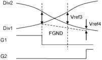
以下说明轻载侦测电路435如何调整开关元件Q1与Q2的导通时间。请同时参阅图7、11A-11B与图12,当整流讯号端耦接至重载时,也就是电流Id相对较高时,讯号Div1、讯号Div2、与虚接地FGND的讯号波形如图11A所示意,由于虚接地FGND的位准大致可以完全跟上线位讯号L与中位讯号N中较低的位准,因此,图7中比较电路433与434的输出(讯号Det1与Det2)将不会变化、或是,讯号Det1与Det2将在讯号G21与G11变化之前,就已经就绪,因此门电路AND1与AND2的输出将会由讯号G21与G11来主控,而不会受讯号Det1与Det2所影响。这表示当整流讯号端耦接至重载时,轻载侦测电路435不会影响开关操作讯号G1与开关操作讯号G2。The following describes how the light
然而,当整流讯号端耦接至轻载时,也就是电流Id相对较低时,讯号Div1、讯号Div2、与虚接地FGND的讯号波形如图11B所示意,由于虚接地FGND的位准无法完全跟上线位讯号L与中位讯号N中较低的位准,故如图所示,讯号Div2低于参考讯号Vref4的时间将会晚于讯号Div1高于[讯号Div2加上参考讯号Vref3]的时间,亦即讯号Det1变化的时间将晚于讯号G21变化的时间,因此门电路AND1的输出将会等待讯号Det1变化之后,才会输出高位准。相似地,门电路AND2的输出也会等待讯号Det2变化之后,才会输出高位准。这表示当整流讯号端耦接至轻载时,轻载侦测电路435调整了开关操作讯号G1与开关操作讯号G2的导通时间,在确定虚接地FGND的位准已经跟上线位讯号L与中位讯号N中较低的位准之后,才导通开关元件Q1或Q2。However, when the rectified signal terminal is coupled to a light load, that is, when the current Id is relatively low, the signal waveforms of the signal Div1, the signal Div2, and the virtual ground FGND are shown in FIG. 11B, because the level of the virtual ground FGND cannot be completely Keep up with the lower level of the upper line signal L and the middle signal N, so as shown in the figure, the time when the signal Div2 is lower than the reference signal Vref4 will be later than the time when the signal Div1 is higher than the [signal Div2 plus the reference signal Vref3] Time, that is, the time when the signal Det1 changes will be later than the time when the signal G21 changes, so the output of the gate circuit AND1 will wait for the signal Det1 to change before outputting a high level. Similarly, the output of the gate circuit AND2 will wait for the signal Det2 to change before outputting a high level. This means that when the rectified signal terminal is coupled to a light load, the light
图8显示本发明第五个实施例。本实施例为控制电路53另一个较具体的实施例。相较于图7所示的第四个实施例,本实施例的控制电路53除包含比较电路331、332、433与434,以及门电路AND1与AND2外,更包含电路536与电路537。电路536例如包含两个去突波电路,分别与门电路AND1与AND2耦接,以对门电路AND1与AND2所产生的讯号进行去突波处理,并将结果输入电路537。电路537例如包含两个操作电路,以接收去突波后的讯号,将其调整至适当位准,并避免开关元件Q1与Q2同时导通,而产生开关操作讯号G1与G2,以操作开关元件Q1与Q2。在电路537中,同时可以设置其它安全上的保护电路,例如过电流保护或过电压保护等,以避免电路损坏,并加入省电模式的功能等,此为相同领域具有通常知识者所熟知,在此不予赘述。Fig. 8 shows a fifth embodiment of the present invention. This embodiment is another more specific embodiment of the
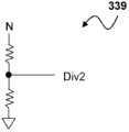
图9A-9B显示本发明第六个实施例。本实施例显示控制电路33、43、或53可更包含分压电路338与339,用以将线位讯号L与中位讯号N分别转换为讯号Div1与讯号Div2,使得讯号Div1与讯号Div2分别正比于线位讯号L与中位讯号N。如图所示,分压电路338与339分别与线位讯号L与中位讯号N耦接,其例如但不限于包含两电阻,并分别取其中一个电阻的跨压作为为讯号Div1与讯号Div2。9A-9B show a sixth embodiment of the present invention. This embodiment shows that the
图13显示本发明在不同应用情况下,电力节省比例的示意图。其中,应用情况的条件如下列:FIG. 13 shows a schematic diagram of power saving ratios of the present invention under different application conditions. Among them, the application conditions are as follows:
应用一App1:输入电压Vin为265Vrms,开关元件Q1与Q2导通电阻Ron为1Ω,分压电阻Rd为10MΩ;Application 1 App1: the input voltage Vin is 265Vrms, the on-resistance Ron of the switching elements Q1 and Q2 is 1Ω, and the voltage divider resistance Rd is 10MΩ;
应用二App2:输入电压Vin为85Vrms,开关元件Q1与Q2导通电阻Ron为1Ω,分压电阻Rd为10MΩ;Application 2 App2: The input voltage Vin is 85Vrms, the on-resistance Ron of switching elements Q1 and Q2 is 1Ω, and the voltage divider resistance Rd is 10MΩ;
应用三App3:输入电压Vin为265Vrms,开关元件Q1与Q2导通电阻Ron为0.5Ω,分压电阻Rd为20MΩ;Application 3 App3: The input voltage Vin is 265Vrms, the on-resistance Ron of the switching elements Q1 and Q2 is 0.5Ω, and the voltage divider resistance Rd is 20MΩ;
应用四App4:输入电压Vin为85Vrms,开关元件Q1与Q2导通电阻Ron为0.5Ω,分压电阻Rd为20MΩ。Application 4 App4: The input voltage Vin is 85Vrms, the on-resistance Ron of the switching elements Q1 and Q2 is 0.5Ω, and the voltage dividing resistor Rd is 20MΩ.
以应用一App1的应用情况为例,当输入电流峰值Ip为0.2A时,也就是图13中的A点所示意,其节省功率比例的计算如下:Taking the application of App1 as an example, when the peak value of the input current Ip is 0.2A, as indicated by point A in Figure 13, the calculation of the power saving ratio is as follows:
PL=VD*Ip=0.6V*0.2A*∫sin(wt)dt/T=0.12W*(-cos(wt))/T=0.12W*2/π=0.076WPL =VD *Ip=0.6V*0.2A*∫sin(wt)dt/T=0.12W*(-cos(wt))/T=0.12W*2/π=0.076W
PRDIV =Vin2/Rd=(265V*√2)2*∫sin2(wt)dt/T/RdPRDIV =Vin2 /Rd=(265V*√2)2 *∫sin2 (wt)dt/T/Rd
=(265V*√2)2*(-1/2*sin(wt)*cos(wt)dt+1/2*∫1dt)/T/Rd=(265V*√2)2 *(-1/2*sin(wt)*cos(wt)dt+1/2*∫1dt)/T/Rd
=70225*2*/2/10MW=0.007W=70225*2*/2/10MW=0.007W
PRon=Ip2*∫sin2(wt)dt*Ron=0.2A2/2*1W=0.02WPRon =Ip2 *∫sin2 (wt)dt*Ron=0.2A2 /2*1W=0.02W
ΔP=0.076W-0.007W-0.02W=0.049WΔP=0.076W-0.007W-0.02W=0.049W
Psave%=ΔP/PL=0.049W/0.076W=64.5%Psave% = ΔP/PL = 0.049W/0.076W = 64.5%
其中,PL为桥式整流电路中二极管的消耗功率,VD为桥式整流电路中二极管的压降,T为输入电流的周期,PRDIV为分压电阻Rd的消耗功率,PRon为开关元件的消耗功率,ΔP为节省功率,Psave%为节省功率比例。由此可以了解,应用本发明节省功率比例相当高,此为本发明优于现有技术的优点之一。Among them, PL is the power consumption of the diode in the bridge rectifier circuit, VD is the voltage drop of the diode in the bridge rectifier circuit, T is the cycle of the input current, PRDIV is the power consumption of the voltage dividing resistor Rd, and PRon is the switch Component power consumption, ΔP is power saving, Psave% is power saving ratio. It can be understood from this that the application of the present invention saves a relatively high proportion of power, which is one of the advantages of the present invention over the prior art.
以上已针对较佳实施例来说明本发明,只是以上所述,仅为使本领域技术人员易于了解本发明的内容,并非用来限定本发明的权利范围。在本发明的相同精神下,本领域技术人员可以思及各种等效变化。例如,开关元件Q1与Q2可为PMOS或NMOS晶体管;在所示各实施例电路中,可插入不影响讯号主要意义的元件,如其它开关等;又例如比较器或误差放大器的输入端正负可以互换,仅需对应修正电路的讯号处理方式即可。凡此种种,皆可根据本发明的教示类推而得,因此,本发明的范围应涵盖上述及其它所有等效变化。The present invention has been described above with reference to preferred embodiments, but the above description is only for those skilled in the art to easily understand the content of the present invention, and is not intended to limit the scope of rights of the present invention. Under the same spirit of the present invention, various equivalent changes can be conceived by those skilled in the art. For example, the switching elements Q1 and Q2 can be PMOS or NMOS transistors; in the circuits of each embodiment shown, elements that do not affect the main meaning of the signal can be inserted, such as other switches; Interchange only needs to correspond to the signal processing method of the correction circuit. All of these can be deduced according to the teaching of the present invention, therefore, the scope of the present invention should cover the above and all other equivalent changes.
Claims (12)
Translated fromChinesePriority Applications (1)
| Application Number | Priority Date | Filing Date | Title |
|---|---|---|---|
| CN201210077526.0ACN103326596B (en) | 2012-03-22 | 2012-03-22 | Power Supply Circuit and AC Signal Rectification Method |
Applications Claiming Priority (1)
| Application Number | Priority Date | Filing Date | Title |
|---|---|---|---|
| CN201210077526.0ACN103326596B (en) | 2012-03-22 | 2012-03-22 | Power Supply Circuit and AC Signal Rectification Method |
Publications (2)
| Publication Number | Publication Date |
|---|---|
| CN103326596Atrue CN103326596A (en) | 2013-09-25 |
| CN103326596B CN103326596B (en) | 2016-08-17 |
Family
ID=49195173
Family Applications (1)
| Application Number | Title | Priority Date | Filing Date |
|---|---|---|---|
| CN201210077526.0AExpired - Fee RelatedCN103326596B (en) | 2012-03-22 | 2012-03-22 | Power Supply Circuit and AC Signal Rectification Method |
Country Status (1)
| Country | Link |
|---|---|
| CN (1) | CN103326596B (en) |
Cited By (4)
| Publication number | Priority date | Publication date | Assignee | Title |
|---|---|---|---|---|
| CN104617794A (en)* | 2015-02-13 | 2015-05-13 | 深圳欧陆通电子有限公司 | Switch power supply and rectifying circuit |
| CN107431385A (en)* | 2015-03-18 | 2017-12-01 | 曼珀斯有限公司 | Wireless power receiver |
| CN110260499A (en)* | 2019-06-13 | 2019-09-20 | 珠海格力电器股份有限公司 | Alternating current signal acquisition device, air conditioner and alternating current signal acquisition method of air conditioner |
| KR20220095344A (en)* | 2020-12-29 | 2022-07-07 | 청주대학교 산학협력단 | Bridgeless type switching rectifier |
Citations (4)
| Publication number | Priority date | Publication date | Assignee | Title |
|---|---|---|---|---|
| JPH10210751A (en)* | 1997-01-22 | 1998-08-07 | Hitachi Ltd | Rectifier circuit, semiconductor integrated circuit, and IC card |
| US20050205679A1 (en)* | 2004-03-17 | 2005-09-22 | Infineon Technologies Ag | Rectifier circuit |
| JP2007020307A (en)* | 2005-07-07 | 2007-01-25 | Shindengen Electric Mfg Co Ltd | Full-wave rectifying circuit |
| JP2012019603A (en)* | 2010-07-07 | 2012-01-26 | Murata Mach Ltd | Non-contact power reception device |
- 2012
- 2012-03-22CNCN201210077526.0Apatent/CN103326596B/ennot_activeExpired - Fee Related
Patent Citations (4)
| Publication number | Priority date | Publication date | Assignee | Title |
|---|---|---|---|---|
| JPH10210751A (en)* | 1997-01-22 | 1998-08-07 | Hitachi Ltd | Rectifier circuit, semiconductor integrated circuit, and IC card |
| US20050205679A1 (en)* | 2004-03-17 | 2005-09-22 | Infineon Technologies Ag | Rectifier circuit |
| JP2007020307A (en)* | 2005-07-07 | 2007-01-25 | Shindengen Electric Mfg Co Ltd | Full-wave rectifying circuit |
| JP2012019603A (en)* | 2010-07-07 | 2012-01-26 | Murata Mach Ltd | Non-contact power reception device |
Cited By (6)
| Publication number | Priority date | Publication date | Assignee | Title |
|---|---|---|---|---|
| CN104617794A (en)* | 2015-02-13 | 2015-05-13 | 深圳欧陆通电子有限公司 | Switch power supply and rectifying circuit |
| CN107431385A (en)* | 2015-03-18 | 2017-12-01 | 曼珀斯有限公司 | Wireless power receiver |
| CN107431385B (en)* | 2015-03-18 | 2020-11-20 | 曼珀斯有限公司 | Wireless power receiver |
| CN110260499A (en)* | 2019-06-13 | 2019-09-20 | 珠海格力电器股份有限公司 | Alternating current signal acquisition device, air conditioner and alternating current signal acquisition method of air conditioner |
| CN110260499B (en)* | 2019-06-13 | 2020-12-25 | 珠海格力电器股份有限公司 | Alternating current signal acquisition device, air conditioner and alternating current signal acquisition method of air conditioner |
| KR20220095344A (en)* | 2020-12-29 | 2022-07-07 | 청주대학교 산학협력단 | Bridgeless type switching rectifier |
Also Published As
| Publication number | Publication date |
|---|---|
| CN103326596B (en) | 2016-08-17 |
Similar Documents
| Publication | Publication Date | Title |
|---|---|---|
| TWI485958B (en) | Control circuit for switching power supply and associated method | |
| CN102412720B (en) | Switching power circuit and power factor correction (PFC) control circuit thereof | |
| EP2658106A1 (en) | Bridgeless power factor correction circuit and method for control thereof | |
| WO2016199497A1 (en) | Power conversion device | |
| CN103326596B (en) | Power Supply Circuit and AC Signal Rectification Method | |
| CN106961094B (en) | The system of input undervoltage and overvoltage protection is provided for supply convertor | |
| CN102694476A (en) | Switch control circuit applied to bridgeless exchange circuit and control method | |
| TW202007059A (en) | Hybrid-mode boost power factor corrector | |
| WO2017020644A1 (en) | Method and apparatus for reducing excitation current of transformer during bypass conducted by isolated ups | |
| US8437153B2 (en) | Series resonant converter capable of reducing peak voltage generated at power switches and peak current generated on secondary side when being turned on from off immediately | |
| CN103904621B (en) | Current-limiting protection with self-recovering function and short-circuit protection circuit | |
| CN104218824B (en) | Bypass device for negative temperature coefficient thermistor | |
| TWI657250B (en) | Current detection method | |
| CN114640240A (en) | Bridgeless power factor correction protection circuit, control method and power module | |
| TWI473412B (en) | Power supply circuit and method for rectifying ac signal | |
| WO2022227070A1 (en) | Power source device, and method for controlling totem-pole pfc circuit | |
| TWI474592B (en) | Bypass apparatus for negative temperature coefficient thermistor | |
| WO2015090184A1 (en) | Method for detecting output conduction angle θ of triac dimmer | |
| CN103124145B (en) | Three-phase rectifier | |
| TWI578684B (en) | Asymmetric half-bridge high step-down converter | |
| TWI717805B (en) | Power supply device | |
| CN101534064A (en) | Power-taking circuit of AC-DC converter | |
| CN117748924A (en) | Surge protection method and circuit | |
| CN112886542A (en) | Current protection circuit, PFC circuit and AC/DC converter | |
| JP2009033814A (en) | DC power supply |
Legal Events
| Date | Code | Title | Description |
|---|---|---|---|
| C06 | Publication | ||
| PB01 | Publication | ||
| C10 | Entry into substantive examination | ||
| SE01 | Entry into force of request for substantive examination | ||
| C14 | Grant of patent or utility model | ||
| GR01 | Patent grant | ||
| CF01 | Termination of patent right due to non-payment of annual fee | Granted publication date:20160817 | |
| CF01 | Termination of patent right due to non-payment of annual fee |