CN103326244A - Photonic crystal laser array with high brightness and horizontal far-field single distribution - Google Patents
Photonic crystal laser array with high brightness and horizontal far-field single distributionDownload PDFInfo
- Publication number
- CN103326244A CN103326244ACN2013102428033ACN201310242803ACN103326244ACN 103326244 ACN103326244 ACN 103326244ACN 2013102428033 ACN2013102428033 ACN 2013102428033ACN 201310242803 ACN201310242803 ACN 201310242803ACN 103326244 ACN103326244 ACN 103326244A
- Authority
- CN
- China
- Prior art keywords
- waveguide
- photonic crystal
- region
- mode
- laser array
- Prior art date
- Legal status (The legal status is an assumption and is not a legal conclusion. Google has not performed a legal analysis and makes no representation as to the accuracy of the status listed.)
- Granted
Links
Images


Landscapes
- Optical Integrated Circuits (AREA)
- Semiconductor Lasers (AREA)
Abstract
Translated fromChinese
Description
Translated fromChinese技术领域technical field
本发明涉及半导体光电子器件技术领域,尤其涉及一种实现高亮度水平远场单瓣分布的光子晶体激光器阵列。The invention relates to the technical field of semiconductor optoelectronic devices, in particular to a photonic crystal laser array for realizing high-brightness far-field single-lobe distribution.
背景技术Background technique
半导体激光器的电光转化效率较高,具有覆盖波段范围广、寿命长、能直接调制、体积小、成本低等优点。其中,边发射半导体激光器阵列在高效率、大功率激光输出方面有着极大的优势,室温下单个激光器巴条连续输出功率已超过百瓦,激光器堆叠输出功率也超过了千瓦。但是其水平方向(平行于pn结平面的方向)的远场特性却不佳,一般表现为双瓣分布,远场发散角很大,降低了激光的亮度。这极大地限制了边发射半导体激光器阵列在很多领域的直接应用。Semiconductor lasers have high electro-optic conversion efficiency and have the advantages of wide coverage, long life, direct modulation, small size, and low cost. Among them, the edge-emitting semiconductor laser array has great advantages in high-efficiency and high-power laser output. The continuous output power of a single laser bar at room temperature has exceeded 100 watts, and the output power of laser stacks has also exceeded kilowatts. However, its far-field characteristics in the horizontal direction (direction parallel to the pn junction plane) are not good, generally showing a double-lobe distribution, and the far-field divergence angle is large, which reduces the brightness of the laser. This greatly limits the direct application of edge-emitting semiconductor laser arrays in many fields.
边发射半导体激光器阵列的水平远场双瓣现象来源于器件内部的模式竞争。在激光器阵列的水平方向上存在很多个模式,因为反相模损耗最低,与增益区的交叠最大,所以在所有模式中占主导地位且最稳定的模式是反相模。反相模在相邻波导的场分布为反相(即相位相差π),正是这一模场分布决定了器件的远场分布为双瓣。国际上有研究小组通过一些特定的结构改变反相模的模场分布来获得单瓣的远场,包括采用外腔波片,在腔面上镀不均匀的膜,以及集成弯折波导阵列等,但这些结构或方法要么工艺复杂,稳定性差,集成度低,要么兼容度不高,损耗大。获得一种兼具有高功率、窄发散角和高稳定性、高集成度的边发射半导体激光器阵列结构,是大家目前努力的重要方向。The horizontal far-field double-lobe phenomenon of edge-emitting semiconductor laser arrays comes from the mode competition inside the device. There are many modes in the horizontal direction of the laser array, because the anti-phase mode has the lowest loss and the largest overlap with the gain region, so the dominant and most stable mode among all modes is the anti-phase mode. The field distribution of the anti-phase mode in adjacent waveguides is anti-phase (that is, the phase difference is π), and it is this mode field distribution that determines the far-field distribution of the device to be double-lobed. There are international research groups that change the mode field distribution of the antiphase mode through some specific structures to obtain a single lobe far field, including using external cavity wave plates, coating uneven films on the cavity surface, and integrating bent waveguide arrays, etc. However, these structures or methods are either complicated in process, poor in stability, low in integration, or not high in compatibility and high in loss. Obtaining an array structure of edge-emitting semiconductor lasers with high power, narrow divergence angle, high stability and high integration is an important direction of our current efforts.
发明内容Contents of the invention
(一)要解决的技术问题(1) Technical problems to be solved
有鉴于此,本发明的主要目的在于提供一种实现高亮度水平远场单瓣分布的光子晶体激光器阵列,通过光子晶体调制相位的功能来解决边发射激光器阵列输出远场为双瓣且发散角大的问题,实现输出高亮度单瓣远场激光的目的。In view of this, the main purpose of the present invention is to provide a photonic crystal laser array that realizes high-brightness level far-field single-lobe distribution, and solve the problem that the output far field of the edge-emitting laser array is double-lobed and the divergence angle is limited by the function of photonic crystal modulation phase. The big problem is to achieve the purpose of outputting high-brightness single-lobe far-field laser.
(二)技术方案(2) Technical solution
本发明提出一种光子晶体激光器阵列,包括两组交替排列的波导:第一波导和第二波导,沿该第一波导和第二波导的传播方向分为三个部分:模式耦合区、光子晶体区和发射区,其中,所述模式耦合区用于产生阵列中相邻波导之间相互耦合的激光模式,并通过模式之间的竞争来输出稳定的反相模式;所述光子晶体区用于通过折射率的周期性变化,对所述模式耦合区中输出的反相模式进行相位调制,使其在相邻波导之间的相位差从180°降低至90°以内,从而将反相模式转换成同相位分布的模式;所述发射区用于将所述光子晶体区中输出的同相位分布的模式从激光器腔面稳定输出,产生一个单瓣远场图案。The present invention proposes a photonic crystal laser array, comprising two sets of alternately arranged waveguides: a first waveguide and a second waveguide, which are divided into three parts along the propagation direction of the first waveguide and the second waveguide: a mode coupling region, a photonic crystal region and an emission region, wherein the mode coupling region is used to generate laser modes coupled between adjacent waveguides in the array, and to output a stable anti-phase mode through competition between the modes; the photonic crystal region is used for Through the periodic change of the refractive index, the antiphase mode output in the mode coupling region is phase modulated, so that the phase difference between adjacent waveguides is reduced from 180° to within 90°, thereby converting the antiphase mode into a mode with the same phase distribution; the emitting region is used to stably output the mode with the same phase distribution output in the photonic crystal region from the laser cavity surface to generate a single lobe far-field pattern.
根据本发明的具体实施方式,所述激光器阵列具有叠层结构,所述叠层结构包括:下电极;形成于该下电极之上的N型衬底;形成于该N型衬底之上的N型限制层;形成于该N型限制层之上的有源层;形成于该有源层之上的P型限制层;形成于该P型限制层之上的P型盖层;形成于该P型盖层之上的SiO2绝缘层;以及形成于该SiO2绝缘层之上的上电极,其中,所述第一波导和第二波导是由刻蚀P型盖层的整个厚度和P型限制层的部分厚度形成。According to a specific embodiment of the present invention, the laser array has a stacked structure, and the stacked structure includes: a lower electrode; an N-type substrate formed on the lower electrode; an N-type substrate formed on the N-type substrate An N-type confinement layer; an active layer formed on the N-type confinement layer; a P-type confinement layer formed on the active layer; a P-type cap layer formed on the P-type confinement layer;SiO2 insulating layer on the P-type capping layer; and an upper electrode formed on theSiO2 insulating layer, wherein the first waveguide and the second waveguide are formed by etching the entire thickness of the P-type capping layer and The partial thickness of the P-type confinement layer is formed.
根据本发明的具体实施方式,所述有源层采用的材料为III-V族半导体材料或II-VI族半导体材料,增益谱峰值波长范围覆盖近紫外到红外波段。According to a specific embodiment of the present invention, the material used for the active layer is a III-V semiconductor material or a II-VI semiconductor material, and the peak wavelength range of the gain spectrum covers near-ultraviolet to infrared bands.
根据本发明的具体实施方式,所述模式耦合区的波导上通过刻蚀或腐蚀所述SiO2绝缘层形成电极窗口。According to a specific embodiment of the present invention, an electrode window is formed on the waveguide of the mode coupling region by etching or corroding the SiO2 insulating layer.
根据本发明的具体实施方式,所述模式耦合区的长度超过光子晶体区长度的两倍。According to a specific embodiment of the present invention, the length of the mode coupling region exceeds twice the length of the photonic crystal region.
根据本发明的具体实施方式,所述第一波导在模式耦合区、光子晶体区和发射区内为均一宽度的第一条形波导;所述第二波导在模式耦合区和发射区内为均一宽度的第二条形波导,在光子晶体区内则包含两个锥形波导和一个第三条形波导。According to a specific embodiment of the present invention, the first waveguide is a first strip waveguide with a uniform width in the mode coupling region, the photonic crystal region and the emission region; the second waveguide is a uniform width in the mode coupling region and the emission region The width of the second strip waveguide contains two tapered waveguides and a third strip waveguide in the photonic crystal region.
根据本发明的具体实施方式,所述第二条形波导的宽度与第一条形波导的宽度相同,比第三条形波导的宽度大,且通过锥形波导和第三条形波导相连。According to a specific embodiment of the present invention, the second strip waveguide has the same width as the first strip waveguide, is larger than the third strip waveguide, and is connected to the third strip waveguide through a tapered waveguide.
根据本发明的具体实施方式,所述锥形波导的长度不超过光子晶体区长度的十分之一。According to a specific embodiment of the present invention, the length of the tapered waveguide does not exceed one tenth of the length of the photonic crystal region.
根据本发明的具体实施方式,所述第三条形波导的长度L由如下公式决定:L=Δψ·λ/(2π·Δn),其中Δψ为通过光子晶体区的调制在第一波导和第二波导的光场之间产生的相移,Δn为在光子晶体区内,第一波导和第二波导中传播的光场之间的有效折射率差。According to a specific embodiment of the present invention, the length L of the third strip waveguide is determined by the following formula: L=Δψ·λ/(2π·Δn), where Δψ is the modulation between the first waveguide and the second waveguide through the photonic crystal region. The phase shift generated between the light fields of the two waveguides, Δn is the effective refractive index difference between the light fields propagating in the first waveguide and the second waveguide in the photonic crystal region.
根据本发明的具体实施方式,所述相移Δψ的范围在(mπ-π/2)~mπ之间,其中m为奇数。According to a specific embodiment of the present invention, the range of the phase shift Δψ is between (mπ-π/2)˜mπ, wherein m is an odd number.
(三)有益效果(3) Beneficial effects
1、本发明提供一种实现高亮度水平远场单瓣分布的光子晶体激光器阵列,利用宽度周期性变化的波导阵列形成对特定光子态具有调控功能的光子晶体,实现对模式的相位调制,将阵列中稳定的反相模式转换成同相分布的模式并输出,从而产生单瓣的水平远场图案,且发散角很窄。1. The present invention provides a photonic crystal laser array that realizes high-brightness level far-field single-lobe distribution, and uses a waveguide array whose width changes periodically to form a photonic crystal that has a control function for a specific photonic state, and realizes the phase modulation of the mode. The stable anti-phase mode in the array is converted to an in-phase distributed mode and output, resulting in a single-lobe horizontal far-field pattern with a narrow divergence angle.
2、本发明的实现高亮度水平远场单瓣分布的光子晶体激光器阵列,结构紧凑,制备工艺简单,易于集成,可产生稳定的高亮度激光。2. The photonic crystal laser array of the present invention that realizes high-brightness level far-field single-lobe distribution has a compact structure, simple manufacturing process, easy integration, and can generate stable high-brightness laser light.
总之,本发明具有直接输出高亮度单瓣水平远场激光的优点,且工艺简单,稳定性高,成本低,在光纤通信、泵浦固态激光器、材料加工等领域中具有广阔的应用前景。In a word, the present invention has the advantages of directly outputting high-brightness single-lobe horizontal far-field laser, and has simple process, high stability, and low cost, and has broad application prospects in the fields of optical fiber communication, pumping solid-state lasers, and material processing.
附图说明Description of drawings
图1为本发明提供的实现高亮度水平远场单瓣分布的光子晶体激光器阵列的三维结构示意图;Fig. 1 is the three-dimensional structure schematic diagram of the photonic crystal laser array that realizes the far-field single lobe distribution of high brightness level provided by the present invention;
图2为本发明的一个实施例的表面几何结构示意图;Fig. 2 is a schematic view of the surface geometry of an embodiment of the present invention;
图3为本发明的一个实施例的反相模在光子晶体区中的二维传输特性图;Fig. 3 is the two-dimensional transmission characteristic diagram of the antiphase mode in the photonic crystal region of an embodiment of the present invention;
图4为本发明的一个实施例的反相模在光子晶体调制前后的相位对比图;Fig. 4 is the phase comparison figure of the inverse mode of an embodiment of the present invention before and after photonic crystal modulation;
图5为本发明的一个实施例的反相模在光子晶体调制前后的水平近场对比图;Fig. 5 is the horizontal near-field comparison diagram of the inverse mode of an embodiment of the present invention before and after photonic crystal modulation;
图6为本发明的一个实施例的反相模在光子晶体调制前后的水平远场对比图。Fig. 6 is a comparison diagram of the horizontal far field of the anti-phase mode before and after photonic crystal modulation according to an embodiment of the present invention.
具体实施方式Detailed ways
本发明通过波导宽度的周期性变化实现波导中光场有效折射率的周期性变化,形成光子晶体。由于光子晶体区中不同波导的有效折射率不同,其中传播的光场之间可产生一定的相位差,此即为光子晶体的相位调制功能。利用相位的调制对反相模式进行相位补偿,改反相特性为同相特性。相比于现有的同类结构,本发明既降低了模式匹配损耗和传输损耗,又兼具了光子晶体结构的稳定性,同时还具有制作方便,易于集成的优点。The invention realizes the periodic change of the effective refractive index of the light field in the waveguide through the periodic change of the waveguide width to form a photonic crystal. Since the effective refractive index of different waveguides in the photonic crystal region is different, a certain phase difference can be generated between the propagating light fields, which is the phase modulation function of the photonic crystal. Use phase modulation to perform phase compensation on the anti-phase mode, and change the anti-phase characteristic to the same-phase characteristic. Compared with the existing structures of the same kind, the invention not only reduces the mode matching loss and the transmission loss, but also has the stability of the photonic crystal structure, and has the advantages of convenient manufacture and easy integration.
为使本发明的目的、技术方案和优点更加清楚明白,以下结合具体实施例,并参照附图,对本发明作进一步的详细说明。In order to make the object, technical solution and advantages of the present invention clearer, the present invention will be further described in detail below in conjunction with specific embodiments and with reference to the accompanying drawings.
图1为本发明提供的实现高亮度水平远场单瓣分布的光子晶体激光器阵列的结构示意图。如图1所示,本发明设计了一种实现高亮度水平远场单瓣分布的光子晶体激光器阵列,该激光器阵列具有叠层结构,该叠层结构包括:下电极101;形成于该下电极之上的N型衬底102;形成于该N型衬底之上的N型限制层103;形成于该N型限制层之上的有源层104;形成于该有源层之上的P型限制层105;形成于该P型限制层之上的P型盖层106;形成于该P型盖层之上的SiO2绝缘层107;以及形成于该SiO2绝缘层之上的上电极108。其中,所述有源层104采用的材料为III-V族半导体材料或II-VI族半导体材料,增益谱峰值波长范围覆盖近紫外到红外波段。FIG. 1 is a schematic structural diagram of a photonic crystal laser array that realizes high-brightness level far-field single-lobe distribution provided by the present invention. As shown in Fig. 1, the present invention has designed a kind of photonic crystal laser array that realizes the far-field single lobe distribution of high brightness level, and this laser array has lamination structure, and this lamination structure comprises:
其中,对于该P型盖层106和该P型限制层105,在平行于该阵列表面的平面的部分区域中,该P型盖层106的整个厚度和该P型限制层105的部分厚度被刻蚀,由此形成两组交替排列的波导:第一波导201和第二波导202。Wherein, for the P-
在该激光器阵列中,沿第一和第二波导的传播方向包括三个部分:模式耦合区203、光子晶体区204和发射区205。In this laser array, three parts are included along the propagation direction of the first and second waveguides: a
模式耦合区203用于产生阵列中相邻波导之间相互耦合的激光模式,模式数目与波导的个数成正比。不同模式之间由于场分布的不同而具有不同的损耗,从而实现模式之间的竞争。因为反相模式的损耗最低,容易实现激射,因此模式耦合区203能够输出稳定的反相模式。The
光子晶体区204通过折射率的周期性变化,对模式耦合区203中输出的反相模式进行相位调制,使其在相邻波导之间的相位差从180°降低至90°以内,从而将反相模式转换成同相位分布的模式;The
发射区205是为了在芯片解理时让腔面位于此区域内,从而保证光子晶体区204的长度的精确性,同时它将光子晶体区204中输出的同相位分布的模式稳定输出至激光器腔面,产生一个窄发散角的单瓣远场图案。The
所述模式耦合区203的长度需超过光子晶体区204长度的两倍,以保证激光器的出射功率。所述在第一波导201和第二波导202的光场之间产生的相移Δψ,其范围应该在(mπ-π/2)~mπ之间,其中m为奇数。The length of the
所述第一波导201在模式耦合区203、光子晶体区204和发射区205内为均一宽度的第一条形波导。所述第二波导202在模式耦合区203和发射区205内为均一宽度的第二条形波导202a,在光子晶体区204则包含两个锥形波导202b和一个第三条形波导202c。The
所述第二条形波导202a的宽度与第一波导201的第一条形波导的宽度相同,比第二波导202的第三条形波导202c宽度大,且通过锥形波导202b和第三条形波导202c相连。The width of the
所述锥形波导202b长度不超过光子晶体区(204)长度的十分之一。The length of the tapered
所述第三条形波导202c的长度L由如下公式决定:L=Δψ·λ/(2π·Δn),其中Δψ为通过光子晶体区204的调制在第一波导201和第二波导202的光场之间产生的相移,Δn为在光子晶体区204内,第一波导201和第二波导202中传播的光场之间的有效折射率差,此有效折射率差与第一波导201和第二波导202的宽度及外延片结构有关。The length L of the
所述模式耦合区203的波导通过刻蚀或腐蚀SiO2绝缘层107形成电极窗口203a。The waveguide of the
以下结合具体的实施例对本发明提供的一种实现高亮度水平远场单瓣分布的光子晶体激光器阵列作进一步详细说明。A photonic crystal laser array that realizes high-brightness level far-field single-lobe distribution provided by the present invention will be further described in detail below in conjunction with specific embodiments.
实施例Example
图2为一种实现高亮度水平远场单瓣分布的光子晶体激光器阵列的一个实施例的表面几何结构示意图。如图所示,该实施例的阵列包含9个波导,在模式耦合区203中,各波导宽度均为5μm,相邻波导间的区域的宽度为2μm,整个耦合区长度为1000μm。在光子晶体区204中,第一条形波导201宽度仍为5μm,第三条形波导202c宽度为2μm。整个光子晶体区长度为300μm,其中两个锥形波导202b长度均为25μm,第三条形波导202c长度为250μm。发射区205内所有波导宽度均为5μm,波导长度均为100μm。整个区域内的波导采用一步刻蚀工艺实现,刻蚀深度约为600nm。Fig. 2 is a schematic diagram of the surface geometric structure of an embodiment of a photonic crystal laser array that realizes high-brightness level far-field single-lobe distribution. As shown in the figure, the array of this embodiment includes 9 waveguides. In the
图3为该实施例的反相模在光子晶体区204中二维传输特性图。反相模在阵列的相邻波导中的相位相差180°,场强是异号的。在相邻波导间非注入的刻蚀区内反相模场强基本为零,因此它与注入载流子有最大的交叠,相对于其它模式具有最低的损耗,最容易产生激射。从图中可以看到,第二波导202中传输的光场在锥形波导202b处有轻微的散射现象,在第三条形波导202c中传输的光场也存在明显的局域现象,而在第一波导201中传输的光场在排除了散射光的影响后变化不大。这些说明光子晶体对阵列中传播的模式场分布进行了调制,相邻波导的光场之间产生了差异。FIG. 3 is a two-dimensional transmission characteristic diagram of the inverse mode in the
图4为该实施例的反相模式经相位调制前后的相位对比图。在经光子晶体区调制之前,模式在相邻波导中的相位相差180°。在相位调制后,模式在相邻波导内的相位差基本都小于90°,即第二波导202中的光场相对于第一波导201中的光场产生了超过90°的相移。虽然在个别波导边界处存在360°的相位突变,但是因为光场在相邻波导交界处的振幅值最小,因此这些极个别的相位突变对输出模式的近场分布影响极小。FIG. 4 is a phase contrast diagram of the anti-phase mode before and after phase modulation in this embodiment. The modes are out of phase by 180° in adjacent waveguides before being modulated by the photonic crystal region. After phase modulation, the phase differences of the modes in adjacent waveguides are basically less than 90°, that is, the optical field in the
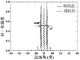
图5为该实施例的反相模式经相位调制前后的近场对比图。从图中可以看到,调制之前的模式在相邻波导中的场强是反号的,这正是180°的相位差造成的。经过相位调制后,第一波导201中的场强的最大值与相邻的第二波导202中的场强是同号的。也就是说,对于相邻波导中的光场,同相的比例要大于反相。由此产生的效果可以从图6中的水平远场分布对比中看出来。调制前的远场为双峰,发散角接近8°。经过相位调制后的远场变成单峰,发散角仅为0.88°,比调制前降低了一个数量级,所以激光器阵列的亮度也提高了一个数量级。这极大地改善了边发射激光器阵列的特性,在工业等领域有巨大的应用潜力。FIG. 5 is a near-field comparison diagram of the anti-phase mode before and after phase modulation in this embodiment. It can be seen from the figure that the field strength of the mode before modulation in the adjacent waveguide is opposite, which is caused by the 180° phase difference. After phase modulation, the maximum value of the field strength in the
以上所述的具体实施例,对本发明的目的、技术方案和有益效果进行了进一步详细说明,应理解的是,以上所述仅为本发明的具体实施例而已,并不用于限制本发明,凡在本发明的精神和原则之内,所做的任何修改、等同替换、改进等,均应包含在本发明的保护范围之内。The specific embodiments described above have further described the purpose, technical solutions and beneficial effects of the present invention in detail. It should be understood that the above descriptions are only specific embodiments of the present invention, and are not intended to limit the present invention. Within the spirit and principles of the present invention, any modifications, equivalent replacements, improvements, etc., shall be included in the protection scope of the present invention.
Claims (10)
Translated fromChinesePriority Applications (1)
| Application Number | Priority Date | Filing Date | Title |
|---|---|---|---|
| CN201310242803.3ACN103326244B (en) | 2013-06-19 | 2013-06-19 | Photonic crystal laser array with high brightness and horizontal far-field single distribution |
Applications Claiming Priority (1)
| Application Number | Priority Date | Filing Date | Title |
|---|---|---|---|
| CN201310242803.3ACN103326244B (en) | 2013-06-19 | 2013-06-19 | Photonic crystal laser array with high brightness and horizontal far-field single distribution |
Publications (2)
| Publication Number | Publication Date |
|---|---|
| CN103326244Atrue CN103326244A (en) | 2013-09-25 |
| CN103326244B CN103326244B (en) | 2015-06-10 |
Family
ID=49194850
Family Applications (1)
| Application Number | Title | Priority Date | Filing Date |
|---|---|---|---|
| CN201310242803.3AActiveCN103326244B (en) | 2013-06-19 | 2013-06-19 | Photonic crystal laser array with high brightness and horizontal far-field single distribution |
Country Status (1)
| Country | Link |
|---|---|
| CN (1) | CN103326244B (en) |
Cited By (4)
| Publication number | Priority date | Publication date | Assignee | Title |
|---|---|---|---|---|
| CN107785776A (en)* | 2017-10-17 | 2018-03-09 | 中国科学院半导体研究所 | Curved tapers photon crystal laser and array, array light source group |
| CN109828420A (en)* | 2019-03-07 | 2019-05-31 | 中国科学院半导体研究所 | A kind of structure inhibiting optical phased array far field sidelobe intensity |
| CN111108655A (en)* | 2017-08-28 | 2020-05-05 | 欧司朗Oled股份有限公司 | Edge-emitting laser bar |
| CN116191205A (en)* | 2023-03-10 | 2023-05-30 | 中国科学院半导体研究所 | Laser array based on topological structure and its fabrication method |
Citations (3)
| Publication number | Priority date | Publication date | Assignee | Title |
|---|---|---|---|---|
| US6810053B1 (en)* | 1999-08-13 | 2004-10-26 | Wisconsin Alumni Research Foundation | Single mode, single lobe surface emitting distributed feedback semiconductor laser |
| US20080192794A1 (en)* | 2007-02-14 | 2008-08-14 | Jacob Meyer Hammer | Lateral-Bragg-Grating-Surface-Emitting Laser/Amplifier (LBGSE) |
| CN102132466A (en)* | 2008-08-28 | 2011-07-20 | Pbc激光股份有限责任公司 | Optoelectronic systems based on field-coupled arrays, line arrays and stacks of semiconductor diode lasers to provide high-power and high-brightness lasers |
- 2013
- 2013-06-19CNCN201310242803.3Apatent/CN103326244B/enactiveActive
Patent Citations (3)
| Publication number | Priority date | Publication date | Assignee | Title |
|---|---|---|---|---|
| US6810053B1 (en)* | 1999-08-13 | 2004-10-26 | Wisconsin Alumni Research Foundation | Single mode, single lobe surface emitting distributed feedback semiconductor laser |
| US20080192794A1 (en)* | 2007-02-14 | 2008-08-14 | Jacob Meyer Hammer | Lateral-Bragg-Grating-Surface-Emitting Laser/Amplifier (LBGSE) |
| CN102132466A (en)* | 2008-08-28 | 2011-07-20 | Pbc激光股份有限责任公司 | Optoelectronic systems based on field-coupled arrays, line arrays and stacks of semiconductor diode lasers to provide high-power and high-brightness lasers |
Cited By (9)
| Publication number | Priority date | Publication date | Assignee | Title |
|---|---|---|---|---|
| CN111108655A (en)* | 2017-08-28 | 2020-05-05 | 欧司朗Oled股份有限公司 | Edge-emitting laser bar |
| CN111108655B (en)* | 2017-08-28 | 2021-07-27 | 欧司朗Oled股份有限公司 | edge-firing laser rods |
| US11411375B2 (en) | 2017-08-28 | 2022-08-09 | Osram Oled Gmbh | Edge-emitting laser bar |
| US11923662B2 (en) | 2017-08-28 | 2024-03-05 | Osram Oled Gmbh | Edge-emitting laser bar |
| CN107785776A (en)* | 2017-10-17 | 2018-03-09 | 中国科学院半导体研究所 | Curved tapers photon crystal laser and array, array light source group |
| CN107785776B (en)* | 2017-10-17 | 2020-03-17 | 中国科学院半导体研究所 | Curved conical photonic crystal laser, array and array light source set |
| CN109828420A (en)* | 2019-03-07 | 2019-05-31 | 中国科学院半导体研究所 | A kind of structure inhibiting optical phased array far field sidelobe intensity |
| CN116191205A (en)* | 2023-03-10 | 2023-05-30 | 中国科学院半导体研究所 | Laser array based on topological structure and its fabrication method |
| CN116191205B (en)* | 2023-03-10 | 2024-01-23 | 中国科学院半导体研究所 | Topological structure-based laser array and manufacturing method thereof |
Also Published As
| Publication number | Publication date |
|---|---|
| CN103326244B (en) | 2015-06-10 |
Similar Documents
| Publication | Publication Date | Title |
|---|---|---|
| CN103904556B (en) | A kind of tiltedly sidewall slope wave guide photon crystal semiconductor laser | |
| CN104092096B (en) | A kind of single mode silicon substrate hybrid laser light source of silicon waveguide output | |
| CN103825194B (en) | Single-mode photon crystal edge-emission semiconductor laser | |
| CN109244828B (en) | A high-power semiconductor laser based on PT Bragg reflection waveguide and its preparation method | |
| US9966734B2 (en) | High speed semiconductor laser with a beam expanding structure | |
| CN103346475B (en) | Monolithic integration coupled cavity narrow linewidth semiconductor laser | |
| CN102611002B (en) | Low Divergence Angle Full Bragg Reflective Waveguide Semiconductor Laser Array | |
| CN108767656A (en) | Coherent source component | |
| CN103326244B (en) | Photonic crystal laser array with high brightness and horizontal far-field single distribution | |
| CN102593719A (en) | Edge-emission semiconductor laser for improving light field distribution of active area | |
| CN101867148B (en) | FP (Fabry-Perot) cavity laser with reflecting surfaces of photonic crystals and vertical emergent surface | |
| CN103915758B (en) | A multi-mode interference structure terahertz quantum cascade laser and its manufacturing method | |
| CN103326243A (en) | Basic transverse mode low-horizontal-divergence-angle one-dimensional chirp photonic crystal edge-emitting laser array | |
| CN102142657A (en) | Manufacturing method of photonic crystal waveguide for improving lateral far field of stripe laser | |
| CN202103312U (en) | Deep sub-wavelength surface plasmon micro-cavity laser | |
| CN104267503B (en) | A kind of metal antenna structure improving face emitting semiconductor laser slow axis far field | |
| CN106575855A (en) | A Vertical Cavity Surface Emitting Laser VCSEL | |
| CN202995205U (en) | Multicore photonic crystal fiber based supercontinuum source | |
| JP2013165201A (en) | Semiconductor optical element, semiconductor optical module and manufacturing method of the same | |
| CN103457156A (en) | Large coupling alignment tolerance semiconductor laser chip applied to high-speed parallel optical transmission and photoelectric device thereof | |
| CN108054634A (en) | A kind of narrow linewidth semiconductor laser | |
| CN103996972A (en) | Photonic crystal edge emitting laser device capable of modulating wave length and divergence angle at the same time | |
| TWI572912B (en) | Light modulator | |
| CN103501200A (en) | Tunable optical chaotic signal generation device and method | |
| CN110277731B (en) | III-V group silicon-based low-refractive-index gap structure DBR laser and integration method |
Legal Events
| Date | Code | Title | Description |
|---|---|---|---|
| C06 | Publication | ||
| PB01 | Publication | ||
| C10 | Entry into substantive examination | ||
| SE01 | Entry into force of request for substantive examination | ||
| C14 | Grant of patent or utility model | ||
| GR01 | Patent grant |