CN103325742A - Semiconductor package substrate and semiconductor package structure - Google Patents
Semiconductor package substrate and semiconductor package structureDownload PDFInfo
- Publication number
- CN103325742A CN103325742ACN2012101569059ACN201210156905ACN103325742ACN 103325742 ACN103325742 ACN 103325742ACN 2012101569059 ACN2012101569059 ACN 2012101569059ACN 201210156905 ACN201210156905 ACN 201210156905ACN 103325742 ACN103325742 ACN 103325742A
- Authority
- CN
- China
- Prior art keywords
- section
- test pad
- pad area
- test
- chip
- Prior art date
- Legal status (The legal status is an assumption and is not a legal conclusion. Google has not performed a legal analysis and makes no representation as to the accuracy of the status listed.)
- Granted
Links
- 239000000758substrateSubstances0.000titleclaimsabstractdescription60
- 239000004065semiconductorSubstances0.000titleclaimsabstractdescription51
- 238000012360testing methodMethods0.000claimsabstractdescription166
- 238000004806packaging method and processMethods0.000claimsabstractdescription13
- 239000004020conductorSubstances0.000claims5
- 239000000463materialSubstances0.000abstractdescription4
- 239000000523sampleSubstances0.000description16
- 238000010586diagramMethods0.000description12
- PXHVJJICTQNCMI-UHFFFAOYSA-NNickelChemical compound[Ni]PXHVJJICTQNCMI-UHFFFAOYSA-N0.000description6
- 239000011521glassSubstances0.000description5
- PCHJSUWPFVWCPO-UHFFFAOYSA-NgoldChemical compound[Au]PCHJSUWPFVWCPO-UHFFFAOYSA-N0.000description5
- 229910052737goldInorganic materials0.000description5
- 239000010931goldSubstances0.000description5
- RYGMFSIKBFXOCR-UHFFFAOYSA-NCopperChemical compound[Cu]RYGMFSIKBFXOCR-UHFFFAOYSA-N0.000description3
- 229910052802copperInorganic materials0.000description3
- 239000010949copperSubstances0.000description3
- 239000004973liquid crystal related substanceSubstances0.000description3
- 229910052759nickelInorganic materials0.000description3
- KDLHZDBZIXYQEI-UHFFFAOYSA-NPalladiumChemical compound[Pd]KDLHZDBZIXYQEI-UHFFFAOYSA-N0.000description2
- 239000004642PolyimideSubstances0.000description2
- 229920001721polyimidePolymers0.000description2
- BQCADISMDOOEFD-UHFFFAOYSA-NSilverChemical compound[Ag]BQCADISMDOOEFD-UHFFFAOYSA-N0.000description1
- ATJFFYVFTNAWJD-UHFFFAOYSA-NTinChemical compound[Sn]ATJFFYVFTNAWJD-UHFFFAOYSA-N0.000description1
- 229910052782aluminiumInorganic materials0.000description1
- XAGFODPZIPBFFR-UHFFFAOYSA-NaluminiumChemical compound[Al]XAGFODPZIPBFFR-UHFFFAOYSA-N0.000description1
- 238000013461designMethods0.000description1
- 238000011161developmentMethods0.000description1
- 238000009713electroplatingMethods0.000description1
- 229910052738indiumInorganic materials0.000description1
- APFVFJFRJDLVQX-UHFFFAOYSA-Nindium atomChemical compound[In]APFVFJFRJDLVQX-UHFFFAOYSA-N0.000description1
- 230000010354integrationEffects0.000description1
- 238000000034methodMethods0.000description1
- 238000012986modificationMethods0.000description1
- 230000004048modificationEffects0.000description1
- 230000005693optoelectronicsEffects0.000description1
- 238000012858packaging processMethods0.000description1
- 229910052763palladiumInorganic materials0.000description1
- 230000000149penetrating effectEffects0.000description1
- 230000001568sexual effectEffects0.000description1
- 229910052709silverInorganic materials0.000description1
- 239000004332silverSubstances0.000description1
- 229910052718tinInorganic materials0.000description1
- 239000011135tinSubstances0.000description1
Images


Classifications
- H—ELECTRICITY
- H01—ELECTRIC ELEMENTS
- H01L—SEMICONDUCTOR DEVICES NOT COVERED BY CLASS H10
- H01L22/00—Testing or measuring during manufacture or treatment; Reliability measurements, i.e. testing of parts without further processing to modify the parts as such; Structural arrangements therefor
- H01L22/30—Structural arrangements specially adapted for testing or measuring during manufacture or treatment, or specially adapted for reliability measurements
- H01L22/32—Additional lead-in metallisation on a device or substrate, e.g. additional pads or pad portions, lines in the scribe line, sacrificed conductors
- H—ELECTRICITY
- H01—ELECTRIC ELEMENTS
- H01L—SEMICONDUCTOR DEVICES NOT COVERED BY CLASS H10
- H01L2224/00—Indexing scheme for arrangements for connecting or disconnecting semiconductor or solid-state bodies and methods related thereto as covered by H01L24/00
- H01L2224/01—Means for bonding being attached to, or being formed on, the surface to be connected, e.g. chip-to-package, die-attach, "first-level" interconnects; Manufacturing methods related thereto
- H01L2224/10—Bump connectors; Manufacturing methods related thereto
- H01L2224/15—Structure, shape, material or disposition of the bump connectors after the connecting process
- H01L2224/16—Structure, shape, material or disposition of the bump connectors after the connecting process of an individual bump connector
- H01L2224/161—Disposition
- H01L2224/16151—Disposition the bump connector connecting between a semiconductor or solid-state body and an item not being a semiconductor or solid-state body, e.g. chip-to-substrate, chip-to-passive
- H01L2224/16221—Disposition the bump connector connecting between a semiconductor or solid-state body and an item not being a semiconductor or solid-state body, e.g. chip-to-substrate, chip-to-passive the body and the item being stacked
- H01L2224/16225—Disposition the bump connector connecting between a semiconductor or solid-state body and an item not being a semiconductor or solid-state body, e.g. chip-to-substrate, chip-to-passive the body and the item being stacked the item being non-metallic, e.g. insulating substrate with or without metallisation
- H01L2224/16238—Disposition the bump connector connecting between a semiconductor or solid-state body and an item not being a semiconductor or solid-state body, e.g. chip-to-substrate, chip-to-passive the body and the item being stacked the item being non-metallic, e.g. insulating substrate with or without metallisation the bump connector connecting to a bonding area protruding from the surface of the item
- H—ELECTRICITY
- H01—ELECTRIC ELEMENTS
- H01L—SEMICONDUCTOR DEVICES NOT COVERED BY CLASS H10
- H01L2224/00—Indexing scheme for arrangements for connecting or disconnecting semiconductor or solid-state bodies and methods related thereto as covered by H01L24/00
- H01L2224/01—Means for bonding being attached to, or being formed on, the surface to be connected, e.g. chip-to-package, die-attach, "first-level" interconnects; Manufacturing methods related thereto
- H01L2224/26—Layer connectors, e.g. plate connectors, solder or adhesive layers; Manufacturing methods related thereto
- H01L2224/31—Structure, shape, material or disposition of the layer connectors after the connecting process
- H01L2224/32—Structure, shape, material or disposition of the layer connectors after the connecting process of an individual layer connector
- H01L2224/321—Disposition
- H01L2224/32151—Disposition the layer connector connecting between a semiconductor or solid-state body and an item not being a semiconductor or solid-state body, e.g. chip-to-substrate, chip-to-passive
- H01L2224/32221—Disposition the layer connector connecting between a semiconductor or solid-state body and an item not being a semiconductor or solid-state body, e.g. chip-to-substrate, chip-to-passive the body and the item being stacked
- H01L2224/32225—Disposition the layer connector connecting between a semiconductor or solid-state body and an item not being a semiconductor or solid-state body, e.g. chip-to-substrate, chip-to-passive the body and the item being stacked the item being non-metallic, e.g. insulating substrate with or without metallisation
- H—ELECTRICITY
- H01—ELECTRIC ELEMENTS
- H01L—SEMICONDUCTOR DEVICES NOT COVERED BY CLASS H10
- H01L2224/00—Indexing scheme for arrangements for connecting or disconnecting semiconductor or solid-state bodies and methods related thereto as covered by H01L24/00
- H01L2224/73—Means for bonding being of different types provided for in two or more of groups H01L2224/10, H01L2224/18, H01L2224/26, H01L2224/34, H01L2224/42, H01L2224/50, H01L2224/63, H01L2224/71
- H01L2224/732—Location after the connecting process
- H01L2224/73201—Location after the connecting process on the same surface
- H01L2224/73203—Bump and layer connectors
- H01L2224/73204—Bump and layer connectors the bump connector being embedded into the layer connector
- H—ELECTRICITY
- H01—ELECTRIC ELEMENTS
- H01L—SEMICONDUCTOR DEVICES NOT COVERED BY CLASS H10
- H01L23/00—Details of semiconductor or other solid state devices
- H01L23/48—Arrangements for conducting electric current to or from the solid state body in operation, e.g. leads, terminal arrangements ; Selection of materials therefor
- H01L23/488—Arrangements for conducting electric current to or from the solid state body in operation, e.g. leads, terminal arrangements ; Selection of materials therefor consisting of soldered or bonded constructions
- H01L23/498—Leads, i.e. metallisations or lead-frames on insulating substrates, e.g. chip carriers
- H01L23/49838—Geometry or layout
Landscapes
- Engineering & Computer Science (AREA)
- Manufacturing & Machinery (AREA)
- Computer Hardware Design (AREA)
- Microelectronics & Electronic Packaging (AREA)
- Power Engineering (AREA)
- Wire Bonding (AREA)
- Testing Of Individual Semiconductor Devices (AREA)
- Testing Or Measuring Of Semiconductors Or The Like (AREA)
Abstract
Translated fromChinese
Description
Translated fromChinese技术领域technical field
本发明关于一种半导体封装基板及半导体封装结构,并且特别地,关于一种具有较大的测试垫尺寸,使探针能确实接触测试垫以避免测试失败的半导体封装基板及半导体封装结构。The present invention relates to a semiconductor packaging substrate and a semiconductor packaging structure, and in particular, to a semiconductor packaging substrate and a semiconductor packaging structure having a larger test pad size so that probes can surely contact the test pad to avoid test failure.
背景技术Background technique
由于光电产业的快速发展,并基于目前电子装置薄型化的潮流,现今的电子装置所使用的显示器均具有厚度薄、大面积及高解析度等优点,如液晶显示器(Liquid Crystal Display,LCD)或等离子体显示器(Plasma Display Panel,PDP)等。上述的薄型显示器的驱动芯片,一般以卷带承载封装(Tape Carrier Package,TCP)或薄膜覆晶封装(Chip on Film,COF)方式对其进行封装。Due to the rapid development of the optoelectronic industry and based on the current trend of thinning electronic devices, the displays used in today's electronic devices have the advantages of thin thickness, large area and high resolution, such as liquid crystal displays (Liquid Crystal Display, LCD) or Plasma Display (Plasma Display Panel, PDP), etc. The driver chip of the above-mentioned thin display is generally packaged in a tape carrier package (Tape Carrier Package, TCP) or a film-on-chip package (Chip on Film, COF).
于目前的TCP/COF封装工艺中,芯片设置于布有引脚的可挠性基板(例如:卷带)上,藉由引脚使芯片与外部电子装置电性连接,以驱动电子装置(如液晶显示器)。于封装后,芯片封装结构需经过测试以确认其功能是否正常,并于测试后才将芯片封装结构自可挠性基板裁切出来。可挠性基板上通常设置有多个连接引脚的测试垫,测试仪器(例如:探针卡)可通过接触这些测试垫来测试芯片的电性功能。In the current TCP/COF packaging process, the chip is placed on a flexible substrate (such as a tape) with pins, and the chip is electrically connected to an external electronic device through the pins to drive the electronic device (such as LCD Monitor). After packaging, the chip package structure needs to be tested to confirm whether its function is normal, and the chip package structure is cut out from the flexible substrate after the test. The flexible substrate is usually provided with a plurality of test pads connecting pins, and a testing instrument (such as a probe card) can test the electrical function of the chip by touching these test pads.
因应现今电子装置轻、薄、短小及多功能的需求,芯片亦必须于缩小尺寸的同时仍具有高集成密度,相应地,可挠性基板上的测试垫数量也必须大幅增加,然而,可挠性基板上的可布线空间有限,为使高密度的测试垫排列于有限的空间中,测试垫通常排列成多排阶梯状。请参阅图1,图1绘示先前技术的TCP/COF芯片封装结构1的示意图,如图1所示,TCP/COF芯片封装结构1的可挠性基材10上可设置芯片16、测试垫12以及连接芯片16与测试垫12的引脚14。于先前技术中,通常输出端测试垫(亦即,图1的右侧测试垫区中的测试垫12)的数量非常多,但测试垫区的空间有限,测试垫12因此排列成多排阶梯状,于此种排列方式,因连接测试垫12的引脚14亦占据测试垫区的部分空间,因此越接近使用区100,测试垫12的尺寸则必须越缩小。In response to the light, thin, short and multi-functional requirements of today's electronic devices, the chip must also have a high integration density while reducing its size. Correspondingly, the number of test pads on the flexible substrate must also be greatly increased. However, flexible The wiring space on the permanent substrate is limited. In order to arrange high-density test pads in the limited space, the test pads are usually arranged in multiple rows of steps. Please refer to FIG. 1. FIG. 1 shows a schematic diagram of a TCP/COF
再者,TCP/COF的芯片封装结构通常是以悬臂式探针卡来进行测试。悬臂式探针卡的探针一般呈斜向配置,当探针卡向下加压使探针接触测试垫时,由于探针斜向接触测试垫,因此易发生滑针的情况,亦即,探针的针尖因压力而于测试垫上滑移并偏离原本预定接触的位置。在较大的测试垫上,例如图1测试垫区中最右排的测试垫12(即最外排测试垫),即便滑针情况发生,探针仍可位于测试垫内,并不影响其电性接触。然而,当测试垫缩小尺寸时,如同图1测试垫区中最内排的测试垫12,在滑针情况发生时探针很容易即滑出测试垫的范围,导致测试结果错误而影响测试的准确性。Furthermore, the chip package structure of TCP/COF is usually tested with a cantilever probe card. The probes of the cantilever probe card are generally arranged obliquely. When the probe card is pressed down to make the probes contact the test pad, since the probes contact the test pad obliquely, the needle slip is prone to occur, that is, Due to the pressure, the tip of the probe slides on the test pad and deviates from the intended contact position. On larger test pads, such as the
发明内容Contents of the invention
因此,本发明的一范畴在于提供一种半导体封装基板及半导体封装结构,以解决先前技术的问题。Therefore, one scope of the present invention is to provide a semiconductor package substrate and a semiconductor package structure to solve the problems of the prior art.
根据一具体实施例,本发明的半导体封装基板包含可挠性基材、测试垫以及引脚。可挠性基材包含互相相对的第一表面与第二表面,其中第一表面上设置有供芯片承载于其上的使用区以及邻接使用区的测试垫区,半导体封装基板及承载于其上的芯片共同形成一半导体封装结构。测试垫设置于测试垫区中,并排列成至少三排。引脚至少形成于使用区上,其一端电性连接设置于使用区中的芯片,且另一端朝向测试垫区延伸并电性连接相对应的测试垫。According to a specific embodiment, the semiconductor package substrate of the present invention includes a flexible substrate, test pads and leads. The flexible base material includes a first surface and a second surface opposite to each other, wherein the first surface is provided with a use area for the chip to be carried thereon and a test pad area adjacent to the use area, and a semiconductor package substrate and a test pad area are carried thereon. The chips jointly form a semiconductor package structure. The test pads are arranged in the test pad area and arranged in at least three rows. The leads are at least formed on the use area, one end of which is electrically connected to the chip disposed in the use area, and the other end extends toward the test pad area and is electrically connected to the corresponding test pad.
于本具体实施例中,连接芯片与位于中间排的测试垫的第一引脚包含第一区段以及第二区段。第一区段具有连接芯片的第一端以及延伸至测试垫区中的第二端,第二区段位于第二表面上,并且其一端连接第一区段的第二端,第二区段另一端则连接到中间排测试垫。藉此,第一表面的测试垫区中可布设空间将会增大,因此可增大位于最内排与中间排的测试垫的尺寸。在进行电性功能的测试时,增大尺寸的测试垫使探针不易滑出测试垫的范围,进而防止测试结果出错而保证测试的准确性。In this specific embodiment, the first pins connecting the chip and the test pads in the middle row include a first segment and a second segment. The first section has a first end connected to the chip and a second end extending into the test pad area, the second section is located on the second surface, and one end thereof is connected to the second end of the first section, the second section The other end is connected to the middle row of test pads. Thereby, the layout space in the test pad area of the first surface will be increased, so the size of the test pads located in the innermost row and the middle row can be increased. When testing the electrical function, the increased size of the test pad makes it difficult for the probe to slip out of the range of the test pad, thereby preventing errors in test results and ensuring the accuracy of the test.
关于本发明的优点与精神可以藉由以下的发明详述及所附附图得到进一步的了解。The advantages and spirit of the present invention can be further understood through the following detailed description of the invention and the accompanying drawings.
附图说明Description of drawings
图1绘示先前技术的TCP/COF芯片封装结构的示意图。FIG. 1 is a schematic diagram of a TCP/COF chip package structure in the prior art.
图2A绘示根据本发明的一具体实施例的半导体封装结构的示意图。FIG. 2A is a schematic diagram of a semiconductor package structure according to an embodiment of the present invention.
图2B绘示图2A的半导体封装结构的剖面示意图。FIG. 2B is a schematic cross-sectional view of the semiconductor package structure in FIG. 2A .
图2C绘示图2A的半导体封装基板的测试垫区的放大示意图。FIG. 2C is an enlarged schematic diagram of the test pad area of the semiconductor package substrate of FIG. 2A .
图3绘示先前技术的卷带式半导体封装结构被裁切出来并电性连接到玻璃基板与印刷电路板的示意图。FIG. 3 is a schematic diagram of a prior art tape and reel semiconductor packaging structure being cut out and electrically connected to a glass substrate and a printed circuit board.
图4A绘示根据本发明的另一具体实施例的半导体封装结构的示意图。FIG. 4A is a schematic diagram of a semiconductor package structure according to another embodiment of the present invention.
图4B绘示图4A的半导体封装基板的测试垫区的放大示意图。FIG. 4B is an enlarged schematic diagram of the test pad area of the semiconductor package substrate of FIG. 4A .
【主要元件符号说明】[Description of main component symbols]
1:TCP/COF芯片封装结构1: TCP/COF chip packaging structure
C1、C2、3:半导体封装结构C1, C2, 3: Semiconductor package structure
2、4:半导体封装基板2, 4: Semiconductor packaging substrate
10、20、30、40:可挠性基材10, 20, 30, 40: flexible substrate
12、22、42:测试垫12, 22, 42: Test pads
14、24、34、44:引脚14, 24, 34, 44: pins
24’、44’:第一引脚24', 44': first pin
34’:外引脚34': external pin
16、50、60:芯片16, 50, 60: chip
26:凸块26: Bump
100、202、402:使用区100, 202, 402: use area
204、404:测试垫区204, 404: test pad area
200、300、400:第一表面200, 300, 400: first surface
206:第二表面206: Second Surface
240:第一区段240: first section
242:第二区段242: Second segment
2420:第一导电插梢2420: First Conductive Pin
2422:第二导电插梢2422: Second Conductive Pin
D:玻璃基板D: glass substrate
P:印刷电路板P: printed circuit board
2020、4020:切割线2020, 4020: Cutting Lines
220、420:最内排220, 420: innermost row
222、422:中间排222, 422: middle row
224、424:最外排224, 424: the outermost row
具体实施方式Detailed ways
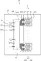
请参阅图2A,图2A绘示根据本发明的一具体实施例的半导体封装结构C1的示意图。如图2A所示,半导体封装结构C1具有半导体封装基板2以及芯片50,其中半导体封装基板2进一步包含可挠性基材20、多个测试垫22以及多个引脚24。于实务中,可挠性基材是以可弯曲的材质所构成,例如,聚亚酰胺(polyimide,PI)。Please refer to FIG. 2A . FIG. 2A is a schematic diagram of a semiconductor package structure C1 according to a specific embodiment of the present invention. As shown in FIG. 2A , the semiconductor package structure C1 has a semiconductor package substrate 2 and a
可挠性基材20具有第一表面200,并且第一表面200上定义出使用区202与测试垫区204,其中,测试垫区204邻接使用区202。芯片50设置于第一表面200上的使用区202之中,各测试垫22则设置于测试垫区204中。于本具体实施例中,上述半导体封装基板2与设置于其上的芯片50共同形成半导体封装结构C1。引脚24设置于第一表面200上且至少形成于使用区202中,并朝向测试垫区204延伸。The
于本具体实施例中,使用区202两侧均邻接有测试垫区204,其中一侧的测试垫区204可为输入端测试垫区(如图2A左侧),另一侧可为输出端测试垫区(如图2A右侧)。一般而言,输出端测试垫数量较输入端测试垫多出许多,由于输出端测试垫数量非常多,因此测试垫22通常会被排列成多个排的配置方式以有效利用测试垫区204的空间。如同图2A所示,位于右侧测试垫区204中的测试垫22依其接近使用区202的距离,依序排列为最内排220、至少一中间排222以及最外排224,请注意,至少一中间排222的排数依测试垫数量而定,并非仅限于本具体实施例中的两排。于其他实施例中,输入端测试垫22亦可根据其数量与测试垫区204的空间限制作多排配置。In this specific embodiment, both sides of the
引脚24连接芯片50与相对应的测试垫22,令使用者可利用探针卡设备,通过探针接触测试垫22来测试芯片50的电性功能。请同时参阅图2B,图2B绘示图2A的半导体封装结构C1的剖面示意图。一般而言,引脚24的一端电性连接芯片50,再经由使用区202延伸到测试垫区204中,使其另一端直接连接对应的测试垫22。于本具体实施例中,连接到左侧测试垫区204的测试垫22以及右侧测试垫区204中最内排220及最外排224的测试垫22的引脚24即为此种设置方式。另一方面,引脚24中包含了第一引脚24’,其一部分设置于第一表面200上且一部分设置于相对可挠性基材20的第一表面200的第二表面206上,这些第一引脚24’可连接到排列于中间排222的测试垫22。芯片50以凸块26电性连接引脚24、24’的一端,其中凸块26例如是电镀凸块,其材质可选自下列群组:金、银、铜、锡、铟、镍/金、镍/钯/金、铜/镍/金、铜/金、铝及其组合。The
如图2B所示,可挠性基材20包含相对于第一表面200的第二表面206,连接到中间排222的测试垫22的第一引脚24’进一步包含了第一区段240以及第二区段242。第一区段240设置于第一表面200上,其具有电性连接芯片50的凸块26的第一端,以及朝向测试垫区204延伸的第二端。第二区段242位于第二表面206上,并且包含有贯穿可挠性基材20的第一导电插梢2420与第二导电插梢2422。第二区段242通过第一导电插梢2420连接到第一区段240的第二端,并通过第二导电插梢2422连接到位于中间排222的测试垫22。As shown in FIG. 2B, the
请再参阅图2C以及图2B,图2C绘示图2A的半导体封装基板2的测试垫区204的放大示意图。如图2C以及图2B所示,位于中间排222的测试垫22与第一引脚24’位于第二表面206的第二区段242电性连接,详言之,这些第一引脚24’的第二区段242设置于测试垫区204投影至第二表面206的范围内,而不占用第一表面200上测试垫区204的空间。如图2C所示,由于第一引脚24’不会穿越第一表面200上的测试垫区204,测试垫区204中可布设测试垫22的尺寸增大,相较于先前技术的设计,位于中间排222以及最内排220的测试垫22获得了较大的可布设空间,故可加大测试垫22的尺寸,使得探针产生滑针或偏移时不致于滑出测试垫22的范围。请注意,图2C所标示的虚线部分根据先前技术所设计的测试垫及引脚的范围,由此可知本发明中位于中间排222与最内排220的测试垫22的尺寸增大。Please refer to FIG. 2C and FIG. 2B again. FIG. 2C is an enlarged schematic diagram of the
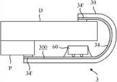
请再参阅图2A,于本具体实施例中,使用区202是由切割线2020所定义,即切割线2020为使用区202与测试垫区204的边界。换言之,于实务中,当测试结束后可将使用区202沿切割线2020裁切出来而形成单个的半导体封装结构,例如:卷带式驱动元件,以进行后续的应用。于实务上,引脚24连接芯片50的一端惯称为内引脚,而引脚24远离芯片50的一端惯称为外引脚,外引脚作为后续连接外部元件之用。请参阅图3,图3绘示先前技术的卷带式半导体封装结构3应用于液晶显示器的局部示意图。如图3所示,卷带式半导体封装结构3的芯片60及引脚34均设置于可挠性基材30的第一表面300之上,当上板时,卷带式半导体封装结构3会被弯折,而分别以位于第一表面300上的输入端及输出端外引脚34’电性连接玻璃基板D及印刷电路板P。若有外引脚同时位于可挠性基材30的二相对表面的情况,将会对后续应用的电性连接造成困难。Please refer to FIG. 2A again. In this embodiment, the
于本具体实施例中,第一引脚24’的第一区段240延伸进入测试垫区204,亦即,第一区段240的第二端位于测试垫区204中,而第二区段242则全部位于测试垫区204投影至第二表面206的范围内。请注意,为了要获得较大的测试垫可布设空间,第一区段240的第二端可终止于切割线2020与最内排220的测试垫22之间,以避免占用过多的测试垫区204面积而影响到最内排220的测试垫22的可布设空间。如图2B所示,基于上述第一引脚24’的配置,于裁切形成单分的半导体封装结构C1后,半导体封装结构C1的引脚24(包含外引脚)均位于第一表面200上,而不会造成上板(亦即,卷带式半导体封装结构连接至玻璃基板与印刷电路板)时的不便。In this specific embodiment, the
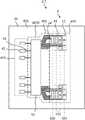
请参阅图4A,图4A绘示根据本发明的另一具体实施例的半导体封装结构C2的示意图。如图4A所示,本具体实施例的半导体封装结构C2包含半导体封装基板4以及芯片50,其中半导体封装基板4进一步包含可挠性基材40、测试垫42、引脚44,其中测试垫42、引脚44以及芯片50均设置于可挠性基材40之上。本具体实施例与上述具体实施例不同处,在于本具体实施例的测试垫42排列于测试垫区404的排列方式不同。本具体实施例的其他单元,与上述具体实施例大体上相同,故于此不再赘述。Please refer to FIG. 4A . FIG. 4A is a schematic diagram of a semiconductor package structure C2 according to another embodiment of the present invention. As shown in FIG. 4A, the semiconductor package structure C2 of this specific embodiment includes a semiconductor package substrate 4 and a
请一并参阅图4B以及图2B,图4B绘示图4A的半导体封装结构C2的测试垫区404的放大示意图。于图4B中,引脚44包含连接位于中间排422的测试垫42的第一引脚44’,第一引脚44’同样可包含第一区段与第二区段,如同图2B所示。第二区段设置于可挠性基材40的第二表面上,故其并不占用测试垫区404的布设空间。同样地,位于中间排422及最内排420的测试垫42可增大其尺寸,以避免测试装置的探针产生滑针或偏移而滑出测试垫42的范围。Please refer to FIG. 4B and FIG. 2B together. FIG. 4B is an enlarged schematic diagram of the
与上述具体实施例相同地,为了要能获得较大的测试垫尺寸并且让裁切下来的半导体封装结构C2便于上板,电性连接位于中间排422的测试垫42的第一引脚44’,其第一区段的第二端终止于切割线4020与最内排420的测试垫42之间,以避免影响最内排420的测试垫42的可布设空间,同时令半导体封装结构C2上的引脚42均位于第一表面。Same as the above-mentioned specific embodiments, in order to obtain a larger test pad size and make the cut-out semiconductor package structure C2 easy to board, electrically connect the first pin 44' of the
相较于先前技术,本发明的半导体封装基板上连接中间排测试垫的引脚部分设置于测试垫所位于的测试垫区的相对表面上,使测试垫区中的测试垫所能布设的空间增大,进而可增大测试垫尺寸,以避免探针发生滑针或偏移时超出测试垫的范围而导致测试失败。此外,各引脚于使用区中的区段完全位于半导体封装基板的同一表面上,因此当使用区自可挠性基材上裁切出来进行电性连接外部元件的作业时,引脚可直接连接玻璃基板及印刷电路板而不会造成上板时的困难。Compared with the prior art, the pin portion connected to the test pads in the middle row on the semiconductor package substrate of the present invention is arranged on the opposite surface of the test pad area where the test pads are located, so that the test pads in the test pad area can be arranged. Increase, and then the size of the test pad can be increased to prevent the probe from slipping or deflecting beyond the range of the test pad, resulting in test failure. In addition, the sections of the pins in the use area are completely located on the same surface of the semiconductor package substrate, so when the use area is cut out from the flexible substrate for the operation of electrically connecting external components, the leads can be directly Connect glass substrates and printed circuit boards without causing difficulties when boarding.
藉由以上较佳具体实施例的详述,是希望能更加清楚描述本发明的特征与精神,而并非以上述所揭露的较佳具体实施例来对本发明的范畴加以限制。相反地,其目的是希望能涵盖各种改变及具相等性的安排于本发明所欲申请的权利要求的范畴内。因此,本发明所申请的权利要求的范畴应该根据上述的说明作最宽广的解释,以致使其涵盖所有可能的改变以及具相等性的安排。Through the above detailed description of the preferred embodiments, it is hoped that the characteristics and spirit of the present invention can be described more clearly, and the scope of the present invention is not limited by the preferred embodiments disclosed above. On the contrary, the intention is to cover various modifications and equivalent arrangements within the scope of the appended claims of the present invention. Therefore, the scope of the claims applied for in the present invention should be interpreted in the broadest way based on the above description, so as to cover all possible changes and arrangements with equivalents.
Claims (10)
Applications Claiming Priority (2)
| Application Number | Priority Date | Filing Date | Title |
|---|---|---|---|
| TW101110027ATWI483361B (en) | 2012-03-23 | 2012-03-23 | Chip packaging substrate and chip packaging structure |
| TW101110027 | 2012-03-23 |
Publications (2)
| Publication Number | Publication Date |
|---|---|
| CN103325742Atrue CN103325742A (en) | 2013-09-25 |
| CN103325742B CN103325742B (en) | 2016-08-03 |
Family
ID=49194411
Family Applications (1)
| Application Number | Title | Priority Date | Filing Date |
|---|---|---|---|
| CN201210156905.9AActiveCN103325742B (en) | 2012-03-23 | 2012-05-18 | Semiconductor package substrate and semiconductor package structure |
Country Status (3)
| Country | Link |
|---|---|
| US (1) | US9082710B2 (en) |
| CN (1) | CN103325742B (en) |
| TW (1) | TWI483361B (en) |
Cited By (3)
| Publication number | Priority date | Publication date | Assignee | Title |
|---|---|---|---|---|
| CN109243996A (en)* | 2018-10-26 | 2019-01-18 | 北京集创北方科技股份有限公司 | A test disk structure and chip test device |
| WO2023071134A1 (en)* | 2021-10-29 | 2023-05-04 | 长鑫存储技术有限公司 | Semiconductor structure and preparation method therefor, and test device |
| WO2023071074A1 (en)* | 2021-10-29 | 2023-05-04 | 长鑫存储技术有限公司 | Semiconductor structure and preparation method therefor, and test system |
Families Citing this family (7)
| Publication number | Priority date | Publication date | Assignee | Title |
|---|---|---|---|---|
| CN103927038B (en)* | 2013-06-09 | 2017-08-29 | 上海天马微电子有限公司 | Embedded touch screen and voltage detection method thereof |
| KR102179035B1 (en)* | 2014-03-07 | 2020-11-16 | 삼성전자주식회사 | Semiconductor device |
| US9748150B2 (en)* | 2015-10-30 | 2017-08-29 | Taiwan Semiconductor Manufacturing Co., Ltd. | Test line structure and method for performing wafer acceptance test |
| KR102525875B1 (en) | 2016-06-24 | 2023-04-27 | 삼성전자주식회사 | Film packages, package modules, and methods of forming packages |
| TWI653717B (en)* | 2017-09-11 | 2019-03-11 | 南茂科技股份有限公司 | Film flip chip package structure |
| KR102565907B1 (en)* | 2017-12-27 | 2023-08-09 | 엘지디스플레이 주식회사 | Display apparatus and electroluminescence display |
| TWI796550B (en)* | 2020-02-26 | 2023-03-21 | 頎邦科技股份有限公司 | Flexible circuit board |
Citations (4)
| Publication number | Priority date | Publication date | Assignee | Title |
|---|---|---|---|---|
| CN1822359A (en)* | 2005-02-15 | 2006-08-23 | 松下电器产业株式会社 | TAB tape and manufacturing method of TAB tape |
| CN1866041A (en)* | 2005-05-18 | 2006-11-22 | 财团法人工业技术研究院 | Device and method for testing built-in components of circuit board |
| CN101226227A (en)* | 2008-02-19 | 2008-07-23 | 日月光半导体制造股份有限公司 | Test carrier board |
| US20090322362A1 (en)* | 2008-06-25 | 2009-12-31 | Samsung Electronics Co., Ltd., | Test pad structure, a pad structure for inspecting a semiconductor chip and a wiring subtrate for a tape package having the same |
Family Cites Families (14)
| Publication number | Priority date | Publication date | Assignee | Title |
|---|---|---|---|---|
| TW276356B (en)* | 1994-06-24 | 1996-05-21 | Ibm | |
| JP3502014B2 (en)* | 2000-05-26 | 2004-03-02 | シャープ株式会社 | Semiconductor device and liquid crystal module |
| KR100505665B1 (en)* | 2003-01-14 | 2005-08-03 | 삼성전자주식회사 | Tape Package having backside test pad and method for electrical testing thereof |
| JP4641141B2 (en)* | 2003-05-28 | 2011-03-02 | ルネサスエレクトロニクス株式会社 | Semiconductor device, TCP type semiconductor device, TCP tape carrier, printed wiring board |
| US6937047B2 (en)* | 2003-08-05 | 2005-08-30 | Freescale Semiconductor, Inc. | Integrated circuit with test pad structure and method of testing |
| JP4492926B2 (en)* | 2003-11-28 | 2010-06-30 | ルネサスエレクトロニクス株式会社 | Semiconductor device |
| CN100589244C (en)* | 2004-03-16 | 2010-02-10 | 松下电器产业株式会社 | Semiconductor device |
| TWI263291B (en)* | 2004-11-15 | 2006-10-01 | Chipmos Technologies Inc | Chip carrier tape having number marking of test pads |
| JP5120868B2 (en)* | 2006-07-13 | 2013-01-16 | ルネサスエレクトロニクス株式会社 | Semiconductor device |
| JP5096782B2 (en)* | 2007-04-19 | 2012-12-12 | ルネサスエレクトロニクス株式会社 | Semiconductor device |
| US9783839B2 (en)* | 2009-05-15 | 2017-10-10 | BIOMéRIEUX, INC. | Automated container management device for microbial detection apparatus |
| JP4864126B2 (en)* | 2009-08-26 | 2012-02-01 | ルネサスエレクトロニクス株式会社 | TCP type semiconductor device |
| US8421073B2 (en)* | 2010-10-26 | 2013-04-16 | Taiwan Semiconductor Manufacturing Company, Ltd. | Test structures for through silicon vias (TSVs) of three dimensional integrated circuit (3DIC) |
| KR20130105163A (en)* | 2012-03-16 | 2013-09-25 | 삼성전자주식회사 | Semiconductor packages and display devices including the same |
- 2012
- 2012-03-23TWTW101110027Apatent/TWI483361B/enactive
- 2012-05-18CNCN201210156905.9Apatent/CN103325742B/enactiveActive
- 2013
- 2013-03-22USUS13/849,294patent/US9082710B2/enactiveActive
Patent Citations (4)
| Publication number | Priority date | Publication date | Assignee | Title |
|---|---|---|---|---|
| CN1822359A (en)* | 2005-02-15 | 2006-08-23 | 松下电器产业株式会社 | TAB tape and manufacturing method of TAB tape |
| CN1866041A (en)* | 2005-05-18 | 2006-11-22 | 财团法人工业技术研究院 | Device and method for testing built-in components of circuit board |
| CN101226227A (en)* | 2008-02-19 | 2008-07-23 | 日月光半导体制造股份有限公司 | Test carrier board |
| US20090322362A1 (en)* | 2008-06-25 | 2009-12-31 | Samsung Electronics Co., Ltd., | Test pad structure, a pad structure for inspecting a semiconductor chip and a wiring subtrate for a tape package having the same |
Cited By (5)
| Publication number | Priority date | Publication date | Assignee | Title |
|---|---|---|---|---|
| CN109243996A (en)* | 2018-10-26 | 2019-01-18 | 北京集创北方科技股份有限公司 | A test disk structure and chip test device |
| WO2023071134A1 (en)* | 2021-10-29 | 2023-05-04 | 长鑫存储技术有限公司 | Semiconductor structure and preparation method therefor, and test device |
| WO2023071074A1 (en)* | 2021-10-29 | 2023-05-04 | 长鑫存储技术有限公司 | Semiconductor structure and preparation method therefor, and test system |
| CN116072563A (en)* | 2021-10-29 | 2023-05-05 | 长鑫存储技术有限公司 | Semiconductor structure and its preparation method, testing system |
| CN116072562A (en)* | 2021-10-29 | 2023-05-05 | 长鑫存储技术有限公司 | Semiconductor structure and its preparation method, testing system |
Also Published As
| Publication number | Publication date |
|---|---|
| US9082710B2 (en) | 2015-07-14 |
| TWI483361B (en) | 2015-05-01 |
| US20130248863A1 (en) | 2013-09-26 |
| CN103325742B (en) | 2016-08-03 |
| TW201340268A (en) | 2013-10-01 |
Similar Documents
| Publication | Publication Date | Title |
|---|---|---|
| CN103325742B (en) | Semiconductor package substrate and semiconductor package structure | |
| KR101726262B1 (en) | Film for package substrate, semiconductor package using the same and display device inclduing the semiconductor package | |
| JP4647139B2 (en) | Contact structure | |
| CN112435619B (en) | Display module and testing method thereof | |
| CN107799561B (en) | display device | |
| US20120262886A1 (en) | Display Device | |
| US20110169792A1 (en) | Display panel | |
| KR100737590B1 (en) | Tab Tape for Tape Carrier Packages | |
| JP2002090424A (en) | Matrix array substrate | |
| CN112748268A (en) | Probe card device | |
| TW201303308A (en) | Probe card | |
| CN111668257A (en) | display device | |
| CN101826505A (en) | Packaging substrate and chip packaging structure | |
| CN103188869B (en) | Flexible printed circuit board | |
| CN101533820A (en) | Chip carrier and chip packaging structure thereof | |
| US20240030123A1 (en) | Electronic apparatus | |
| CN1877347A (en) | Method for measuring contact impedance and structure thereof | |
| CN116758839A (en) | A display device and a detection method thereof | |
| CN102097158A (en) | Anisotropic conductive film structure | |
| KR20170135601A (en) | Chip on printed circuit film and display apparatus comprising the same | |
| TWI474458B (en) | Chip packaging substrate | |
| CN100412658C (en) | Display and crystal coated glass packaging structure | |
| JP3853729B2 (en) | Flexible printed wiring board connection structure and connection method | |
| KR100835431B1 (en) | How to test a semiconductor package | |
| TW201032304A (en) | Package substrate and chip package structure |
Legal Events
| Date | Code | Title | Description |
|---|---|---|---|
| C06 | Publication | ||
| PB01 | Publication | ||
| C10 | Entry into substantive examination | ||
| SE01 | Entry into force of request for substantive examination | ||
| C14 | Grant of patent or utility model | ||
| GR01 | Patent grant |