CN103311454A - Electronic device with reduced non-device edge area and manufacturing method thereof - Google Patents
Electronic device with reduced non-device edge area and manufacturing method thereofDownload PDFInfo
- Publication number
- CN103311454A CN103311454ACN2013100841572ACN201310084157ACN103311454ACN 103311454 ACN103311454 ACN 103311454ACN 2013100841572 ACN2013100841572 ACN 2013100841572ACN 201310084157 ACN201310084157 ACN 201310084157ACN 103311454 ACN103311454 ACN 103311454A
- Authority
- CN
- China
- Prior art keywords
- substrate
- edge
- barrier film
- article
- devices
- Prior art date
- Legal status (The legal status is an assumption and is not a legal conclusion. Google has not performed a legal analysis and makes no representation as to the accuracy of the status listed.)
- Granted
Links
Images


Classifications
- H—ELECTRICITY
- H10—SEMICONDUCTOR DEVICES; ELECTRIC SOLID-STATE DEVICES NOT OTHERWISE PROVIDED FOR
- H10K—ORGANIC ELECTRIC SOLID-STATE DEVICES
- H10K59/00—Integrated devices, or assemblies of multiple devices, comprising at least one organic light-emitting element covered by group H10K50/00
- H10K59/90—Assemblies of multiple devices comprising at least one organic light-emitting element
- H—ELECTRICITY
- H01—ELECTRIC ELEMENTS
- H01L—SEMICONDUCTOR DEVICES NOT COVERED BY CLASS H10
- H01L25/00—Assemblies consisting of a plurality of semiconductor or other solid state devices
- H01L25/03—Assemblies consisting of a plurality of semiconductor or other solid state devices all the devices being of a type provided for in a single subclass of subclasses H10B, H10D, H10F, H10H, H10K or H10N, e.g. assemblies of rectifier diodes
- H01L25/04—Assemblies consisting of a plurality of semiconductor or other solid state devices all the devices being of a type provided for in a single subclass of subclasses H10B, H10D, H10F, H10H, H10K or H10N, e.g. assemblies of rectifier diodes the devices not having separate containers
- H01L25/075—Assemblies consisting of a plurality of semiconductor or other solid state devices all the devices being of a type provided for in a single subclass of subclasses H10B, H10D, H10F, H10H, H10K or H10N, e.g. assemblies of rectifier diodes the devices not having separate containers the devices being of a type provided for in group H10H20/00
- H01L25/0753—Assemblies consisting of a plurality of semiconductor or other solid state devices all the devices being of a type provided for in a single subclass of subclasses H10B, H10D, H10F, H10H, H10K or H10N, e.g. assemblies of rectifier diodes the devices not having separate containers the devices being of a type provided for in group H10H20/00 the devices being arranged next to each other
- H—ELECTRICITY
- H10—SEMICONDUCTOR DEVICES; ELECTRIC SOLID-STATE DEVICES NOT OTHERWISE PROVIDED FOR
- H10K—ORGANIC ELECTRIC SOLID-STATE DEVICES
- H10K50/00—Organic light-emitting devices
- H10K50/80—Constructional details
- H—ELECTRICITY
- H10—SEMICONDUCTOR DEVICES; ELECTRIC SOLID-STATE DEVICES NOT OTHERWISE PROVIDED FOR
- H10K—ORGANIC ELECTRIC SOLID-STATE DEVICES
- H10K50/00—Organic light-emitting devices
- H10K50/80—Constructional details
- H10K50/84—Passivation; Containers; Encapsulations
- H10K50/844—Encapsulations
- H—ELECTRICITY
- H10—SEMICONDUCTOR DEVICES; ELECTRIC SOLID-STATE DEVICES NOT OTHERWISE PROVIDED FOR
- H10K—ORGANIC ELECTRIC SOLID-STATE DEVICES
- H10K59/00—Integrated devices, or assemblies of multiple devices, comprising at least one organic light-emitting element covered by group H10K50/00
- H10K59/30—Devices specially adapted for multicolour light emission
- H10K59/32—Stacked devices having two or more layers, each emitting at different wavelengths
- H—ELECTRICITY
- H10—SEMICONDUCTOR DEVICES; ELECTRIC SOLID-STATE DEVICES NOT OTHERWISE PROVIDED FOR
- H10K—ORGANIC ELECTRIC SOLID-STATE DEVICES
- H10K59/00—Integrated devices, or assemblies of multiple devices, comprising at least one organic light-emitting element covered by group H10K50/00
- H10K59/80—Constructional details
- H10K59/87—Passivation; Containers; Encapsulations
- H10K59/873—Encapsulations
- H10K59/8731—Encapsulations multilayered coatings having a repetitive structure, e.g. having multiple organic-inorganic bilayers
- H—ELECTRICITY
- H10—SEMICONDUCTOR DEVICES; ELECTRIC SOLID-STATE DEVICES NOT OTHERWISE PROVIDED FOR
- H10K—ORGANIC ELECTRIC SOLID-STATE DEVICES
- H10K71/00—Manufacture or treatment specially adapted for the organic devices covered by this subclass
- H—ELECTRICITY
- H01—ELECTRIC ELEMENTS
- H01L—SEMICONDUCTOR DEVICES NOT COVERED BY CLASS H10
- H01L2924/00—Indexing scheme for arrangements or methods for connecting or disconnecting semiconductor or solid-state bodies as covered by H01L24/00
- H01L2924/0001—Technical content checked by a classifier
- H01L2924/0002—Not covered by any one of groups H01L24/00, H01L24/00 and H01L2224/00
- H—ELECTRICITY
- H10—SEMICONDUCTOR DEVICES; ELECTRIC SOLID-STATE DEVICES NOT OTHERWISE PROVIDED FOR
- H10K—ORGANIC ELECTRIC SOLID-STATE DEVICES
- H10K50/00—Organic light-emitting devices
- H10K50/80—Constructional details
- H10K50/805—Electrodes
- H—ELECTRICITY
- H10—SEMICONDUCTOR DEVICES; ELECTRIC SOLID-STATE DEVICES NOT OTHERWISE PROVIDED FOR
- H10K—ORGANIC ELECTRIC SOLID-STATE DEVICES
- H10K71/00—Manufacture or treatment specially adapted for the organic devices covered by this subclass
- H10K71/851—Division of substrate
- Y—GENERAL TAGGING OF NEW TECHNOLOGICAL DEVELOPMENTS; GENERAL TAGGING OF CROSS-SECTIONAL TECHNOLOGIES SPANNING OVER SEVERAL SECTIONS OF THE IPC; TECHNICAL SUBJECTS COVERED BY FORMER USPC CROSS-REFERENCE ART COLLECTIONS [XRACs] AND DIGESTS
- Y02—TECHNOLOGIES OR APPLICATIONS FOR MITIGATION OR ADAPTATION AGAINST CLIMATE CHANGE
- Y02E—REDUCTION OF GREENHOUSE GAS [GHG] EMISSIONS, RELATED TO ENERGY GENERATION, TRANSMISSION OR DISTRIBUTION
- Y02E10/00—Energy generation through renewable energy sources
- Y02E10/50—Photovoltaic [PV] energy
- Y02E10/549—Organic PV cells
- Y—GENERAL TAGGING OF NEW TECHNOLOGICAL DEVELOPMENTS; GENERAL TAGGING OF CROSS-SECTIONAL TECHNOLOGIES SPANNING OVER SEVERAL SECTIONS OF THE IPC; TECHNICAL SUBJECTS COVERED BY FORMER USPC CROSS-REFERENCE ART COLLECTIONS [XRACs] AND DIGESTS
- Y02—TECHNOLOGIES OR APPLICATIONS FOR MITIGATION OR ADAPTATION AGAINST CLIMATE CHANGE
- Y02P—CLIMATE CHANGE MITIGATION TECHNOLOGIES IN THE PRODUCTION OR PROCESSING OF GOODS
- Y02P70/00—Climate change mitigation technologies in the production process for final industrial or consumer products
- Y02P70/50—Manufacturing or production processes characterised by the final manufactured product
Landscapes
- Engineering & Computer Science (AREA)
- Physics & Mathematics (AREA)
- Inorganic Chemistry (AREA)
- Chemical & Material Sciences (AREA)
- Power Engineering (AREA)
- Microelectronics & Electronic Packaging (AREA)
- Optics & Photonics (AREA)
- Manufacturing & Machinery (AREA)
- Condensed Matter Physics & Semiconductors (AREA)
- Computer Hardware Design (AREA)
- General Physics & Mathematics (AREA)
- Electroluminescent Light Sources (AREA)
- Photovoltaic Devices (AREA)
Abstract
Translated fromChineseDescription
Translated fromChinese技术领域technical field
本申请案涉及具有减少的非装置边缘区的电子装置和其制造方法。The present application relates to electronic devices with reduced non-device edge regions and methods of manufacturing the same.
背景技术Background technique
利用有机材料的光电装置由于许多原因而正在变得日益合乎需要。许多用于制造这些装置的材料相对便宜,因此,有机光电装置有潜力在成本上优于无机装置。另外,有机材料的内在特性,例如其柔性,可使其非常适合于具体的应用,例如在柔性衬底上制作。有机光电装置的实例包括有机发光装置(OLED)、有机光敏晶体管、有机光电池和有机光检测器。对于OLED,有机材料在性能上可优于常规材料。举例来说,有机发射层发光的波长一般可通过适当的掺杂剂容易进行调整。Optoelectronic devices utilizing organic materials are becoming increasingly desirable for a number of reasons. Many of the materials used to make these devices are relatively inexpensive, so organic optoelectronic devices have the potential to be cost-effective compared to inorganic devices. In addition, the intrinsic properties of organic materials, such as their flexibility, can make them well suited for specific applications, such as fabrication on flexible substrates. Examples of organic optoelectronic devices include organic light emitting devices (OLEDs), organic phototransistors, organic photovoltaic cells, and organic photodetectors. For OLEDs, organic materials can outperform conventional materials in performance. For example, the wavelength of light emitted by the organic emission layer can generally be easily adjusted by appropriate dopants.
OLED利用薄的有机膜,这些有机膜在对整个装置施加电压时发光。OLED正在变成一项日益引起关注的技术,用于例如平板显示器、照明和背光等应用。若干OLED材料和配置描述于美国专利第5,844,363号、第6,303,238号和第5,707,745号中,这些专利以全文引用的方式并入本文中。OLEDs utilize thin organic films that emit light when a voltage is applied across the device. OLEDs are becoming an increasingly interesting technology for applications such as flat panel displays, lighting and backlighting. Several OLED materials and configurations are described in US Patent Nos. 5,844,363, 6,303,238, and 5,707,745, which are incorporated herein by reference in their entirety.
磷光发射分子的一个应用是全色显示器。此类显示器的行业标准需要适宜于发射具体的颜色(称为“饱和”颜色)的像素。具体地说,这些标准需要饱和红色、绿色和蓝色像素。颜色可使用此项技术熟知的CIE座标来测量。One application of phosphorescent emitting molecules is in full-color displays. The industry standard for such displays requires pixels adapted to emit a specific color, called a "saturated" color. Specifically, these standards require saturated red, green and blue pixels. Color can be measured using CIE coordinates well known in the art.
绿色发射分子的一个实例是三(2-苯基吡啶)铱(表示为Ir(ppy)3),其具有式I的结构:An example of a green emitting molecule is tris(2-phenylpyridine)iridium (denoted Ir(ppy)3), which has the structure of formula I:

在此图和本文中后面的图中,将氮到金属(此处为Ir)的配价键描绘为直线。In this figure and in the figures later in this text, the coordinate bond of nitrogen to the metal (here Ir) is depicted as a straight line.
如本文所用,术语“有机”包括可用于制作有机光电装置的聚合物材料以及小分子有机材料。“小分子”是指任何非聚合物有机材料,并且“小分子”实际上可能很大。在某些情况下小分子可包括重复单元。举例来说,使用长链烷基作为取代基不会将一个分子从“小分子”类别中去除。小分子也可以并入聚合物中,例如作为聚合物主链上的侧基或作为主链的一部分。小分子也可以用作树枝状聚合物的核心部分,此树枝状聚合物由建造于核心部分上的一系列化学外壳组成。树枝状聚合物的核心部分可以是荧光或磷光小分子发射体。树枝状聚合物可以是“小分子”,并且相信所有目前用于OLED领域的树枝状聚合物都是小分子。As used herein, the term "organic" includes polymeric materials as well as small molecule organic materials that can be used to fabricate organic optoelectronic devices. By "small molecule" is meant any non-polymeric organic material, and a "small molecule" may actually be quite large. In some cases small molecules may include repeating units. For example, the use of long chain alkyl groups as substituents does not remove a molecule from the "small molecule" category. Small molecules can also be incorporated into polymers, for example as pendant groups on the polymer backbone or as part of the backbone. Small molecules can also be used as the core part of dendrimers, which consist of a series of chemical shells built on the core part. The core portion of the dendrimer can be a fluorescent or phosphorescent small molecule emitter. Dendrimers can be "small molecules" and it is believed that all dendrimers currently used in the field of OLEDs are small molecules.
如本文所用,“顶”意指离衬底最远,而“底”意指最靠近衬底。在描述第一层是“安置在”第二层之上的情况下,此第一层远离衬底安置。除非说明第一层“接触”第二层,否则在第一与第二层之间可存在其它层。举例来说,阴极可描述成是“安置在”阳极之上,即使中间存在多个有机层。As used herein, "top" means furthest from the substrate, and "bottom" means closest to the substrate. Where it is described that a first layer is "disposed over" a second layer, this first layer is disposed remotely from the substrate. There may be other layers between the first and second layers unless it is stated that the first layer "contacts" the second layer. For example, a cathode may be described as being "disposed over" an anode, even though there are multiple organic layers in between.
如本文所用,“溶液可加工的”意指能够在液体介质中溶解、分散或传递和/或从液体介质沉积,呈溶液或悬浮液形式。As used herein, "solution processable" means capable of being dissolved, dispersed or transported in and/or deposited from a liquid medium, either in the form of a solution or a suspension.
当相信配体直接有助于发射材料的光敏性特性时,配体可称为“光敏性的”。当相信配体无助于发射材料的光敏性特性时,配体可称为“辅助性的”,不过辅助性配体可改变光敏性配体的特性。A ligand may be referred to as "photosensitive" when it is believed that the ligand directly contributes to the photosensitivity properties of the emissive material. A ligand may be referred to as "ancillary" when it is believed that the ligand does not contribute to the photosensitivity properties of the emissive material, although ancillary ligands may alter the properties of the photosensitizing ligand.
如本文所用并且如所属领域的技术人员一般所了解,如果第一“最高占有分子轨道”(HOMO)或“最低未占分子轨道”(LUMO)能级更接近真空能级,那么此第一能级“超过”或“高于”第二HOMO或LUMO能级。因为电离电位(IP)相对于真空能级测量为负能量,所以较高的HOMO能级对应于具有较小绝对值的IP(负值较大的IP)。类似地,较高LUMO能级对应于具有较小绝对值的电子亲和力(EA)(负值较大的EA)。在常规的能级图上,在真空能级在顶部的情况下,一材料的LUMO能级高于同一材料的HOMO能级。“较高”HOMO或LUMO能级看上去比“较低”HOMO或LUMO能级更靠近此类图的顶部。As used herein and as generally understood by those skilled in the art, if the first "highest occupied molecular orbital" (HOMO) or "lowest unoccupied molecular orbital" (LUMO) energy level is closer to the vacuum level, then the first energy The level is "over" or "higher than" the second HOMO or LUMO energy level. Because the ionization potential (IP) is measured as a negative energy relative to the vacuum level, higher HOMO levels correspond to IPs with smaller absolute values (more negative IPs). Similarly, a higher LUMO energy level corresponds to an electron affinity (EA) with a smaller absolute value (a more negative EA). On a conventional energy level diagram, with the vacuum level at the top, the LUMO energy level of a material is higher than the HOMO energy level of the same material. "Higher" HOMO or LUMO energy levels appear to be closer to the top of such graphs than "lower" HOMO or LUMO energy levels.
如本文所用并且如所属领域的技术人员一般所了解,如果第一功函数具有较高的绝对值,那么此第一功函数“超过”或“高于”第二功函数。因为功函数一般相对于真空能级测量为负数,所以此意味着“较高”功函数的负值较小。在常规的能级图上,在真空能级在顶部的情况下,“较高”功函数说明为在向下的方向上远离真空能级。因此,HOMO和LUMO能级的定义按照不同于功函数的约定。As used herein and as generally understood by those skilled in the art, a first work function "exceeds" or is "higher than" a second work function if the first work function has a higher absolute value. Since work functions are generally measured as negative relative to the vacuum level, this means that "higher" work functions are less negative. On a conventional energy level diagram, with the vacuum level at the top, "higher" work functions are illustrated as being in a downward direction away from the vacuum level. Therefore, the definitions of HOMO and LUMO energy levels follow a different convention than the work function.
有关OLED和上述定义的更多详情可见于美国专利第7,279,704号中,此专利以全文引用的方式并入本文中。Further details regarding OLEDs and the above definitions can be found in US Patent No. 7,279,704, which is hereby incorporated by reference in its entirety.
发明内容Contents of the invention
本文提供的一些实施例可包含一种装置、用于制造装置的方法和/或通过一种工艺制备的装置,其在不会增加由大气条件引起的降级的情况下减少或消除装置的非装置(或“死角”)。也就是说,例如,本文提供的实施例可包含一种装置,其中此装置的一部分可安置在衬底的边缘或边缘附近,通过利用安置在衬底的垂直侧面和/或边缘(以及装置的侧面)的至少一部分之上的障壁膜作为边缘密封,不会增加装置降级。这样一来,跨越障壁膜与衬底的界面的进入(其通常比跨越障壁膜整体快)可在不在垂直于装置侧面的方向上扩展障壁膜层下维持足够的长度,而在垂直于装置侧面的方向上扩展障壁膜层在一些情况下会产生额外的装置的非装置。Some embodiments provided herein may include a device, method for making a device, and/or a device made by a process that reduces or eliminates non-device (or "dead spots"). That is, for example, embodiments provided herein may include a device wherein a portion of the device may be positioned at or near an edge of a substrate by utilizing The barrier film over at least a portion of the sides) acts as an edge seal without increasing device degradation. In this way, entry across the interface of the barrier film to the substrate, which is typically faster than across the bulk of the barrier film, can be maintained of sufficient length without extending the barrier film layer in a direction perpendicular to the device sides, but in a direction perpendicular to the device sides. Extending the barrier film in the direction of the non-device will in some cases create additional devices.
在一些实施例中,可提供第一制品。所述第一制品可包含衬底,所述衬底具有第一表面、第一侧面和第一边缘,其中所述第一表面与所述第一侧面相接;和安置在所述衬底之上的装置,所述装置具有第二侧面,其中所述第二侧面的至少第一部分在离所述衬底的所述第一边缘约3mm内安置。第一制品可进一步包含第一障壁膜,所述第一障壁膜覆盖所述衬底的所述第一边缘的至少一部分、所述衬底的所述第一侧面的至少一部分和所述装置的所述第二侧面的至少所述第一部分。In some embodiments, a first article may be provided. The first article may comprise a substrate having a first surface, a first side, and a first edge, wherein the first surface is contiguous with the first side; and disposed between the substrate The device on has a second side, wherein at least a first portion of the second side is disposed within about 3 mm of the first edge of the substrate. The first article may further comprise a first barrier film covering at least a portion of the first edge of the substrate, at least a portion of the first side of the substrate, and a portion of the device. At least the first portion of the second side.
在一些实施例中,在如上所述的第一制品中,所述装置的所述第二侧面的至少所述第一部分可在离所述衬底的所述第一边缘约2mm内安置。在一些实施例中,所述装置的所述第二侧面的至少所述第一部分可在离所述衬底的所述第一边缘约1mm内安置。在一些实施例中,所述装置的所述第二侧面的至少所述第一部分可在离所述衬底的所述第一边缘约0.5mm内安置。在一些实施例中,所述装置的所述第二侧面的至少所述第一部分可在离所述衬底的所述第一边缘约0.1mm内安置。In some embodiments, in the first article as described above, at least the first portion of the second side of the device can be disposed within about 2 mm of the first edge of the substrate. In some embodiments, at least the first portion of the second side of the device can be disposed within about 1 mm of the first edge of the substrate. In some embodiments, at least the first portion of the second side of the device can be disposed within about 0.5 mm of the first edge of the substrate. In some embodiments, at least the first portion of the second side of the device can be disposed within about 0.1 mm of the first edge of the substrate.
在一些实施例中,在如上所述的第一制品中,所述装置可包含作用装置区和非作用装置区,并且所述装置的所述作用装置区的至少一部分可在离所述衬底的所述第一边缘0.1mm内安置。In some embodiments, in the first article as described above, the device may comprise an active device region and a non-active device region, and at least a portion of the active device region of the device may be within a distance from the substrate placed within 0.1mm of the first edge.
在一些实施例中,在如上所述的第一制品中,所述装置可包含作用装置区,并且所述装置的所述作用装置区的至少一部分可在离所述衬底的所述第一边缘0.1mm内安置。In some embodiments, in the first article as described above, the device may comprise an active device region, and at least a portion of the active device region of the device may be within a distance from the first substrate of the substrate. Placed within 0.1mm of the edge.
在一些实施例中,在如上所述的第一制品中,所述衬底可包含以下任一者:玻璃、塑料或金属箔片材料。In some embodiments, in the first article as described above, the substrate may comprise any of: glass, plastic, or metal foil material.
在一些实施例中,在如上所述的第一制品中,所述第一障壁膜可包含聚合物材料与非聚合物材料的混合物。在一些实施例中,所述第一障壁膜可包含聚合硅与无机硅的混合物。In some embodiments, in the first article as described above, the first barrier film may comprise a mixture of a polymeric material and a non-polymeric material. In some embodiments, the first barrier film may include a mixture of polymeric silicon and inorganic silicon.
在一些实施例中,在如上所述的第一制品中,所述第一障壁膜可安置在所述装置的至少一部分之上。在一些实施例中,所述第一障壁膜可安置在整个装置之上。In some embodiments, in the first article as described above, the first barrier film can be disposed over at least a portion of the device. In some embodiments, the first barrier film can be disposed over the entire device.
在一些实施例中,在如上所述的第一制品中,所述装置可包含多个侧面并且所述第一障壁膜可覆盖所述装置的所述多个侧面中的每一个。在一些实施例中,所述衬底可包含多个侧面,并且所述第一障壁膜可覆盖所述衬底的所述多个侧面中的每一个的至少一部分。在一些实施例中,所述衬底可包含四个侧面并且所述第一障壁膜可覆盖衬底的这些侧面中的至少两个的至少一部分。在一些实施例中,所述第一障壁膜可安置在整个装置之上。In some embodiments, in the first article as described above, the device can comprise a plurality of sides and the first barrier film can cover each of the plurality of sides of the device. In some embodiments, the substrate may include a plurality of sides, and the first barrier film may cover at least a portion of each of the plurality of sides of the substrate. In some embodiments, the substrate can include four sides and the first barrier film can cover at least a portion of at least two of the sides of the substrate. In some embodiments, the first barrier film can be disposed over the entire device.
在一些实施例中,在如上所述的第一制品中,所述第一制品可进一步包含第二障壁膜,所述第二障壁膜可安置在所述装置之上。所述第一障壁膜和所述第二障壁膜可包含不同的材料。在一些实施例中,所述第二障壁膜可包含玻璃、塑料、涂有障壁膜的塑料或金属箔片材料。In some embodiments, in the first article as described above, the first article can further comprise a second barrier film, the second barrier film can be disposed over the device. The first barrier film and the second barrier film may include different materials. In some embodiments, the second barrier film may comprise glass, plastic, plastic coated with a barrier film, or a metal foil material.
在一些实施例中,在如上所述的第一制品中,所述衬底可具有第一外周长,并且所述装置可具有第二外周长。在一些实施例中,所述装置的所述第二外周长的至少约50%可在离所述衬底的所述第一外周长约1mm内安置。在一些实施例中,所述装置的所述第二外周长的至少约50%可在离所述衬底的所述第一外周长约0.1mm内安置。在一些实施例中,所述装置的所述第二外周长的至少约75%可在离所述衬底的所述第一外周长约1mm内安置。在一些实施例中,所述装置的所述第二外周长的至少约75%可在离所述衬底的所述第一外周长约0.1mm内安置。In some embodiments, in the first article as described above, the substrate can have a first outer perimeter and the device can have a second outer perimeter. In some embodiments, at least about 50% of the second outer perimeter of the device can be disposed within about 1 mm of the first outer perimeter of the substrate. In some embodiments, at least about 50% of the second outer perimeter of the device can be disposed within about 0.1 mm of the first outer perimeter of the substrate. In some embodiments, at least about 75% of the second outer perimeter of the device can be disposed within about 1 mm of the first outer perimeter of the substrate. In some embodiments, at least about 75% of the second outer perimeter of the device can be disposed within about 0.1 mm of the first outer perimeter of the substrate.
在一些实施例中,在如上所述的第一制品中,所述第一障壁膜可使用化学气相沉积CVD和有机硅前体沉积。In some embodiments, in the first article as described above, the first barrier film can be deposited using chemical vapor deposition CVD and an organosilicon precursor.
在一些实施例中,所述第一制品可包含以下任一者:太阳能电池、薄膜电池、有机电子装置、照明面板或具有照明面板的照明源、显示器或具有显示器的电子装置、移动式电话、笔记本式计算机、平板计算机或电视。In some embodiments, the first article of manufacture may comprise any of the following: a solar cell, a thin film battery, an organic electronic device, a lighting panel or a lighting source with a lighting panel, a display or an electronic device with a display, a mobile phone, Laptop, tablet or TV.
在一些实施例中,在如上所述的第一制品中,所述装置可包含有机层。在一些实施例中,所述装置包括OLED。In some embodiments, in the first article as described above, the device may comprise an organic layer. In some embodiments, the device includes an OLED.
在一些实施例中,在如上所述的第一制品中,所述第一制品可进一步包含电子器件封装,其中所述电子器件封装具有至少一种小于装置的尺寸。在一些实施例中,所述电子器件封装的总面积小于装置的总面积。In some embodiments, in the first article as described above, the first article may further comprise an electronic device package, wherein the electronic device package has at least one dimension smaller than the device. In some embodiments, the total area of the electronic device package is less than the total area of the device.
在一些实施例中,在如上所述的第一制品中,所述第一制品可进一步包含多个装置。在一些实施例中,所述多个装置中的每一个可离其它装置中的至少一个不到6.0mm的距离安置。在一些实施例中,所述多个装置中的每一个可离其它装置中的至少一个不到4.0mm的距离安置。在一些实施例中,所述多个装置中的每一个可离其它装置中的至少一个不到2.0mm的距离安置。在一些实施例中,所述多个装置中的每一个可离其它装置中的至少一个不到1.0mm的距离安置。In some embodiments, in the first article as described above, the first article may further comprise a plurality of devices. In some embodiments, each of the plurality of devices may be positioned less than 6.0 mm from at least one of the other devices. In some embodiments, each of the plurality of devices may be positioned less than 4.0 mm from at least one of the other devices. In some embodiments, each of the plurality of devices may be positioned less than 2.0 mm from at least one of the other devices. In some embodiments, each of the plurality of devices may be positioned less than 1.0 mm from at least one of the other devices.
在一些实施例中,在如上所述的第一制品中,在所述第一制品包含多个装置的情况下,所述多个装置可安置在相同的衬底上。在一些实施例中,所述多个装置可安置在不同的衬底上。在一些实施例中,所述多个装置可包含至少两个发射具有不同峰值波长的光的装置。在一些实施例中,所述第一制品可包含显示器。In some embodiments, in the first article as described above, where the first article comprises a plurality of devices, the plurality of devices may be disposed on the same substrate. In some embodiments, the multiple devices may be disposed on different substrates. In some embodiments, the plurality of devices may include at least two devices that emit light having different peak wavelengths. In some embodiments, the first article may comprise a display.
在一些实施例中,在如上所述的第一制品中,所述衬底可进一步包含第二表面并且多个导电体可安置在所述衬底内,其中所述多个导体中的每一个都从所述衬底的所述第一表面延伸到所述第二表面。在一些实施例中,所述导电体中的每一个都可安置在微孔内。在一些实施例中,所述衬底可包含外周长并且所述多个导体中的每一个可在所述外周长的1mm内安置。在一些实施例中,在所述衬底包含外周长的情况下,所述导体中的至少一个可离所述衬底的所述外周长超过1mm的距离安置。In some embodiments, in the first article as described above, the substrate can further comprise a second surface and a plurality of electrical conductors can be disposed within the substrate, wherein each of the plurality of conductors both extend from the first surface to the second surface of the substrate. In some embodiments, each of the electrical conductors can be disposed within a microwell. In some embodiments, the substrate can include an outer perimeter and each of the plurality of conductors can be disposed within 1 mm of the outer perimeter. In some embodiments, where the substrate includes an outer perimeter, at least one of the conductors may be disposed at a distance of more than 1 mm from the outer perimeter of the substrate.
在一些实施例中,在如上所述的第一制品中,所述第一制品可进一步包含多个导电体,所述多个导电体可安置在所述衬底的所述第一侧面上。在一些实施例中,所述衬底可进一步包含第二表面并且所述多个导电体中的每一个可从所述衬底的所述第一表面延伸到所述第二表面。In some embodiments, in the first article as described above, the first article may further comprise a plurality of electrical conductors, the plurality of electrical conductors may be disposed on the first side of the substrate. In some embodiments, the substrate can further include a second surface and each of the plurality of electrical conductors can extend from the first surface of the substrate to the second surface.
在一些实施例中,在如上所述的衬底包含第二表面并且多个导体安置在衬底内或安置在衬底的第一侧面上的第一制品中,所述第一制品可进一步包含多个安置在所述衬底之上的电极。在一些实施例中,所述多个导电体中的每一个都可电连接到所述多个电极中的至少一个。在一些实施例中,所述多个电极与所述多个导电体之间的所述电连接可包含安置在所述衬底的所述第一表面上的图案化的导电迹线。In some embodiments, in a first article as described above wherein the substrate includes a second surface and the plurality of conductors are disposed within the substrate or on the first side of the substrate, the first article may further comprise A plurality of electrodes are disposed over the substrate. In some embodiments, each of the plurality of electrical conductors is electrically connectable to at least one of the plurality of electrodes. In some embodiments, the electrical connections between the plurality of electrodes and the plurality of electrical conductors can include patterned conductive traces disposed on the first surface of the substrate.
在一些实施例中,可提供一种第一制品,所述第一制品包含第一衬底,所述第一衬底具有第一表面、第一侧面和第一边缘,其中所述第一表面与所述第一侧面相接;第二衬底,所述第二衬底具有第一表面、第一侧面和第一边缘,其中所述第一表面与所述第一侧面相接;和包含第一装置与第二装置的多个装置。所述第一装置可安置在所述第一衬底之上并且具有第二侧面,其中所述第一装置的所述第二侧面的至少第一部分在离所述第一衬底的所述第一边缘约3.0mm内安置。所述第一制品可进一步包含第一障壁膜,所述第一障壁膜覆盖所述第一衬底的所述第一边缘的至少一部分、所述第一衬底的所述第一侧面的至少一部分和所述第一装置的所述第二侧面的至少所述第一部分。所述第二装置可安置在所述第二衬底之上并且具有第二侧面,其中所述第二装置的所述第二侧面的至少第一部分在离所述第二衬底的所述第一边缘约3.0mm内安置。所述第一制品可进一步包括第二障壁膜,所述第二障壁膜覆盖所述第二衬底的所述第一边缘的至少一部分、所述第二衬底的所述第一侧面的至少一部分和所述第二装置的所述第二侧面的至少所述第一部分。In some embodiments, there may be provided a first article comprising a first substrate having a first surface, a first side, and a first edge, wherein the first surface adjoining the first side; a second substrate having a first surface, a first side, and a first edge, wherein the first surface adjoins the first side; and comprising Multiple devices of the first device and the second device. The first device may be disposed over the first substrate and have a second side, wherein at least a first portion of the second side of the first device is at a distance from the first substrate of the second side. One edge is placed within about 3.0mm. The first article may further comprise a first barrier film covering at least a portion of the first edge of the first substrate, at least a portion of the first side of the first substrate, A portion and at least the first portion of the second side of the first device. The second device may be disposed over the second substrate and have a second side, wherein at least a first portion of the second side of the second device is at a distance from the second substrate of the second substrate. One edge is placed within about 3.0mm. The first article may further include a second barrier film covering at least a portion of the first edge of the second substrate, at least a portion of the first side of the second substrate, A portion and at least said first portion of said second side of said second device.
在一些实施例中,在如上所述的第一制品中,所述第一装置的所述第二侧面的所述第一部分可离所述第二装置的所述第二侧面的所述第一部分不到6.0mm的距离安置。在一些实施例中,所述第一装置的所述第二侧面的所述第一部分可离所述第二装置的所述第二侧面的所述第一部分不到2.0mm的距离安置。在一些实施例中,所述第一装置的所述第二侧面的所述第一部分可离所述第二装置的所述第二侧面的所述第一部分不到1.0mm的距离安置。In some embodiments, in the first article as described above, the first portion of the second side of the first device is separable from the first portion of the second side of the second device Placement at a distance of less than 6.0mm. In some embodiments, the first portion of the second side of the first device may be positioned a distance of less than 2.0 mm from the first portion of the second side of the second device. In some embodiments, the first portion of the second side of the first device may be positioned a distance of less than 1.0 mm from the first portion of the second side of the second device.
在一些实施例中,在如上所述的第一制品中,所述第一装置可包含作用装置区和非作用装置区;所述第二装置可包含作用装置区和非作用装置区;并且所述第一装置的所述作用装置区的至少一部分离所述第二装置的所述作用装置区的至少一部分不到1.0mm的距离安置。In some embodiments, in the first article as described above, the first device may comprise an active device region and a non-active device region; the second device may comprise an active device region and a non-active device region; and the At least a portion of said active device region of said first device is positioned less than 1.0 mm from at least a portion of said active device region of said second device.
在一些实施例中,在如上所述的第一制品中,所述第一装置可包含作用装置区;所述第二装置可包含作用装置区;并且所述第一装置的所述作用装置区的至少一部分离所述第二装置的所述作用装置区的至少一部分不到0.01mm的距离安置。In some embodiments, in the first article as described above, the first device may comprise an active device region; the second device may comprise an active device region; and the active device region of the first device At least a portion of at least a portion of said active device region of said second device is positioned at a distance of less than 0.01 mm from at least a portion of said active device region of said second device.
实施例还可提供一种第一方法。所述第一方法可包括以下步骤:提供衬底,所述衬底具有:第一表面、第一侧面和第一边缘,其中所述第一表面与所述第一侧面相接;和安置在所述衬底的所述第一表面之上的装置,所述装置具有第二侧面。所述装置的所述第二侧面的至少第一部分可离所述衬底的所述第一边缘不超过3.0mm安置。在提供衬底后,所述第一方法进一步包括将第一障壁膜沉积以便覆盖所述衬底的所述第一边缘的至少一部分、所述衬底的所述第一侧面的至少一部分和所述装置的所述第二侧面的至少所述第一部分的步骤。Embodiments may also provide a first method. The first method may include the steps of: providing a substrate having: a first surface, a first side, and a first edge, wherein the first surface adjoins the first side; A device on the first surface of the substrate, the device having a second side. At least a first portion of the second side of the device may be disposed no more than 3.0 mm from the first edge of the substrate. After providing the substrate, the first method further includes depositing a first barrier film so as to cover at least a portion of the first edge of the substrate, at least a portion of the first side of the substrate, and all at least said first portion of said second side of said device.
在一些实施例中,在如上所述的第一方法中,所述第二侧面的至少所述第一部分可离所述第一边缘起不超过2.0mm安置。在一些实施例中,所述第二侧面的至少所述第一部分可离所述第一边缘不超过1.0mm安置。在一些实施例中,所述第二侧面的至少所述第一部分可离所述第一边缘不超过0.5mm安置。在一些实施例中,所述第二侧面的至少所述第一部分可离所述第一边缘不超过0.1mm安置。In some embodiments, in the first method as described above, at least the first portion of the second side may be positioned no more than 2.0 mm from the first edge. In some embodiments, at least the first portion of the second side may be positioned no more than 1.0 mm from the first edge. In some embodiments, at least the first portion of the second side may be located no more than 0.5 mm from the first edge. In some embodiments, at least the first portion of the second side may be located no more than 0.1 mm from the first edge.
在一些实施例中,在如上所述的第一方法中,所述装置可包含作用装置区;并且所述装置的所述作用装置区的至少一部分可在离所述衬底的所述第一边缘0.1mm内安置。In some embodiments, in the first method as described above, the device may comprise an active device region; and at least a portion of the active device region of the device may be within a distance of the first Placed within 0.1mm of the edge.
在一些实施例中,在如上所述的第一方法中,所述第一障壁膜可包含聚合物材料与非聚合物材料的混合物。在一些实施例中,所述第一障壁膜可包含聚合硅与无机硅的混合物。In some embodiments, in the first method as described above, the first barrier film may comprise a mixture of a polymeric material and a non-polymeric material. In some embodiments, the first barrier film may include a mixture of polymeric silicon and inorganic silicon.
在一些实施例中,在如上所述的第一方法中,所述提供衬底的步骤可包括以下步骤:在多个位置刻划所述衬底,将所述装置沉积在所述衬底的所述第一表面之上,并且在所述多个刻划位置处使所述衬底断裂。在一些实施例中,所述使所述衬底断裂的步骤可在将所述装置沉积在所述衬底的所述第一表面之上前进行。在一些实施例中,所述使所述衬底断裂的步骤可在将所述装置沉积在所述衬底的所述第一表面之上后进行。In some embodiments, in the first method as described above, the step of providing the substrate may include the steps of scribing the substrate at a plurality of locations, depositing the device on the substrate breaking the substrate over the first surface and at the plurality of score locations. In some embodiments, the step of breaking the substrate can be performed before depositing the device on the first surface of the substrate. In some embodiments, the step of breaking the substrate can be performed after depositing the device over the first surface of the substrate.
在一些实施例中,在如上所述的第一方法中,所述提供衬底的步骤可包括以下步骤:将所述装置沉积在所述衬底的所述第一表面之上;在将所述装置沉积后,在多个位置处刻划所述衬底和所述装置;以及在所述多个刻划位置处使所述衬底和所述装置断裂。In some embodiments, in the first method as described above, the step of providing the substrate may include the steps of: depositing the device on the first surface of the substrate; After the device is deposited, scoring the substrate and the device at a plurality of locations; and breaking the substrate and the device at the plurality of scribed locations.
在一些实施例中,在如上所述的第一方法中,所述提供衬底的步骤可包括将所述装置沉积在所述衬底的整个第一表面之上的步骤。在一些实施例中,所述提供衬底的步骤可包括通过具有大于所述衬底的所述第一表面的开口的掩模将所述装置沉积的步骤。In some embodiments, in the first method as described above, the step of providing a substrate may comprise the step of depositing the device over the entire first surface of the substrate. In some embodiments, the step of providing a substrate may comprise the step of depositing the device through a mask having openings larger than the first surface of the substrate.
在一些实施例中,在如上所述的第一方法中,所述提供衬底的步骤可包括以下步骤:将所述装置沉积在所述衬底的所述第一表面之上;以及在将所述装置沉积后,在多个位置处使所述衬底和所述装置断裂。在一些实施例中,所述使所述衬底和所述装置断裂的步骤可包含切割所述装置和所述衬底。In some embodiments, in the first method as described above, the step of providing a substrate may include the steps of: depositing the device on the first surface of the substrate; After the device is deposited, the substrate and the device are fractured at various locations. In some embodiments, the step of breaking the substrate and the device can include cutting the device and the substrate.
在一些实施例中,在如上所述的第一方法中,所述提供衬底的步骤可包括以下步骤:将所述装置沉积在所述衬底的所述第一表面之上;在将所述装置沉积后,切削作用区的一部分以暴露所述装置的所述第二侧面;以及在所述装置沉积后,切削所述衬底的一部分以暴露所述第一侧面。In some embodiments, in the first method as described above, the step of providing the substrate may include the steps of: depositing the device on the first surface of the substrate; After the device is deposited, cutting a portion of the active area to expose the second side of the device; and after the device is deposited, cutting a portion of the substrate to expose the first side.
在一些实施例中,在如上所述的第一方法中,在将所述第一障壁膜沉积后,所述方法可进一步包含使所述衬底断裂的步骤。In some embodiments, in the first method as described above, after depositing the first barrier film, the method may further include the step of breaking the substrate.
在一些实施例中,在如上所述的第一方法中,所述第一方法可进一步包含从所述衬底的所述第一表面到所述衬底的第二表面形成多个导电通路的步骤。在一些实施例中,所述形成多个导电通路的步骤可包括以下步骤:在所述衬底中制作多个从所述第一表面到所述第二表面的通孔;和将导电材料安置在所述多个通孔中的每一个中。In some embodiments, in the first method as described above, the first method may further include forming a plurality of conductive vias from the first surface of the substrate to the second surface of the substrate step. In some embodiments, the step of forming a plurality of conductive paths may include the steps of: making a plurality of via holes in the substrate from the first surface to the second surface; and disposing a conductive material in each of the plurality of through holes.
在一些实施例中,在如上所述的包含从衬底的第一表面到衬底的第二表面形成多个导电通路的步骤的第一方法中,所述形成多个导电通路的步骤可包含将导电材料安置在所述衬底的所述第一侧面上。在一些实施例中,所述将导电材料安置在所述衬底的所述第一侧面上的步骤包含以下的任一者或某些组合:将所述导电材料直接印刷在所述第一侧面的一部分之上以用于所述多个导电通路;将导电层安置在所述第一侧面的至少一部分之上并且使所述导电层图案化以形成所述多个导电通路;使用真空工艺将导电层沉积以形成所述多个导电通路;和/或将所述衬底的所述第一侧面浸渍到导电材料中以便形成所述多个导电通路。In some embodiments, in the first method as described above comprising the step of forming a plurality of conductive paths from the first surface of the substrate to the second surface of the substrate, the step of forming the plurality of conductive paths may include A conductive material is disposed on the first side of the substrate. In some embodiments, the step of disposing a conductive material on the first side of the substrate comprises any one or some combination of the following: printing the conductive material directly on the first side for the plurality of conductive paths; disposing a conductive layer over at least a portion of the first side and patterning the conductive layer to form the plurality of conductive paths; using a vacuum process to depositing a conductive layer to form the plurality of conductive paths; and/or dipping the first side of the substrate into a conductive material to form the plurality of conductive paths.
实施例还可提供一种第一制品,所述第一制品通过一种工艺制备。所述工艺可包括以下步骤:提供衬底,所述衬底具有第一表面、第一侧面和第一边缘,其中所述第一表面与所述第一侧面相接;和安置在所述衬底的所述第一表面之上的具有第二侧面的装置,其中所述第二侧面的至少第一部分离所述第一边缘不超过1.0mm安置。所述工艺可进一步包括将第一障壁膜沉积以便覆盖所述衬底的所述第一边缘的至少一部分、所述衬底的所述第一侧面的至少一部分和所述第二侧面的至少所述第一部分的步骤。Embodiments may also provide a first article prepared by a process. The process may include the steps of: providing a substrate having a first surface, a first side, and a first edge, wherein the first surface adjoins the first side; and disposing on the substrate A device having a second side on said first surface of a bottom, wherein at least a first portion of said second side is positioned no more than 1.0 mm from said first edge. The process may further include depositing a first barrier film so as to cover at least a portion of the first edge of the substrate, at least a portion of the first side of the substrate, and at least all of the second side of the substrate. Steps in the first part.
在一些实施例中,在通过如上所述的工艺制备的第一制品中,所述第一障壁膜可包含聚合物材料与非聚合物材料的混合物。In some embodiments, in the first article prepared by the process described above, the first barrier film may comprise a mixture of polymeric material and non-polymeric material.
在一些实施例中,在通过如上所述的工艺制备的第一制品中,所述将所述第一障壁膜沉积的步骤可包含使用有机硅前体。在一些实施例中,所述将所述第一障壁膜沉积的步骤可包含化学气相沉积CVD。在一些实施例中,所述化学气相沉积可以是等离子体增强的。In some embodiments, in the first article prepared by the process described above, the step of depositing the first barrier film may comprise using an organosilicon precursor. In some embodiments, the step of depositing the first barrier film may include chemical vapor deposition (CVD). In some embodiments, the chemical vapor deposition can be plasma enhanced.
在一些实施例中,在通过如上所述的其中将第一障壁膜沉积的步骤包含使用有机硅前体进行气相沉积的工艺制备的第一制品中,所述障壁膜可基本上由聚合硅与无机硅的混合物组成。在一些实施例中,聚合硅与无机硅的重量比可在95∶5到5∶95范围内。在一些实施例中,聚合硅与无机硅可由相同的前体材料产生。在一些实施例中,可在对于沉积工艺中的所有反应条件来说都相同的反应条件下沉积至少0.1μm厚的障壁膜。在一些实施例中,通过所述至少0.1μm厚的障壁膜的水蒸气传输速率可小于每天10-6g/m2。In some embodiments, in the first article prepared by the process as described above wherein the step of depositing the first barrier film comprises vapor deposition using an organosilicon precursor, the barrier film can consist essentially of polymeric silicon and A mixture of inorganic silicon. In some embodiments, the weight ratio of polymeric silicon to inorganic silicon may range from 95:5 to 5:95. In some embodiments, polymeric silicon and inorganic silicon can be produced from the same precursor material. In some embodiments, a barrier film at least 0.1 μm thick can be deposited under the same reaction conditions for all reaction conditions in the deposition process. In some embodiments, the water vapor transmission rate through the at least 0.1 μm thick barrier film may be less than 10−6 g/m2 per day.
在一些实施例中,在通过如上所述的其中将第一障壁膜沉积的步骤包含使用有机硅前体进行气相沉积的工艺制备的第一制品中,所述前体材料可包含六甲基二硅氧烷或二甲基硅氧烷。在一些实施例中,所述前体材料可包含单一有机硅化合物。在一些实施例中,所述前体材料包含有机硅化合物的混合物。In some embodiments, in the first article prepared by the process as described above wherein the step of depositing the first barrier film comprises vapor deposition using an organosilicon precursor, the precursor material may comprise hexamethyldi Silicone or Dimethicone. In some embodiments, the precursor material may comprise a single organosilicon compound. In some embodiments, the precursor material comprises a mixture of organosilicon compounds.
实施例还可提供一种第一制品。所述第一制品可包含衬底,所述衬底具有第一表面、第一侧面和第一边缘,其中所述第一表面与所述第一侧面相接;和安置在所述衬底之上的具有第二侧面的装置;其中所述第二侧面的至少第一部分在离所述衬底的所述第一边缘约1.0mm内安置。所述装置可包含第一有机材料。在一些实施例中,所述第一衬底的所述第一侧面无部分经超过6×10¹³个原子/平方厘米的第一有机材料覆盖。Embodiments may also provide a first article. The first article may comprise a substrate having a first surface, a first side, and a first edge, wherein the first surface is contiguous with the first side; and disposed between the substrate The device having a second side on the above; wherein at least a first portion of the second side is disposed within about 1.0 mm of the first edge of the substrate. The device can include a first organic material. In some embodiments, no portion of the first side of the first substrate is covered with more than 6×10¹³ atoms/
在一些实施例中,在如上所述的第一制品中,所述第一有机材料不覆盖所述衬底的所述第一侧面的任何部分。In some embodiments, in the first article as described above, the first organic material does not cover any portion of the first side of the substrate.
在一些实施例中,如上所述的第一制品可进一步包含第一障壁膜,所述第一障壁膜覆盖所述衬底的所述第一边缘的至少一部分、所述衬底的所述第一侧面的至少一部分和所述装置的所述第二侧面的至少所述第一部分。In some embodiments, the first article as described above may further include a first barrier film covering at least a portion of the first edge of the substrate, the first at least a portion of one side and at least said first portion of said second side of said device.
在一些实施例中,在如上所述的第一制品中,所述装置的所述第二侧面的至少所述第一部分可在离所述衬底的所述第一边缘约0.1mm内安置。In some embodiments, in the first article as described above, at least the first portion of the second side of the device can be disposed within about 0.1 mm of the first edge of the substrate.
实施例还可提供一种第一方法。所述第一方法可包括以下步骤:提供衬底,所述衬底具有:第一表面、第一侧面和第一边缘,其中所述第一表面与所述第一侧面相接;和安置在所述衬底的第一表面之上的装置;以及使所述装置断裂以便暴露所述装置的第二侧面,使得所述装置的至少第一部分离所述第一边缘不超过3.0mm安置。在一些实施例中,所述装置的至少所述第一部分可离所述第一边缘不超过2.0mm安置。在一些实施例中,所述装置的至少所述第一部分可离所述第一边缘不超过1.0mm安置。在一些实施例中,所述装置的至少所述第一部分离所述第一边缘不超过0.1mm安置。Embodiments may also provide a first method. The first method may include the steps of: providing a substrate having: a first surface, a first side, and a first edge, wherein the first surface adjoins the first side; a device over the first surface of the substrate; and breaking the device so as to expose a second side of the device such that at least a first portion of the device is positioned no more than 3.0 mm from the first edge. In some embodiments, at least the first portion of the device may be positioned no more than 2.0 mm from the first edge. In some embodiments, at least the first portion of the device may be positioned no more than 1.0 mm from the first edge. In some embodiments, at least said first portion of said device is positioned no more than 0.1 mm from said first edge.
在一些实施例中,在如上所述的第一方法中,所述装置可包含作用装置区;并且所述装置的所述作用装置区的至少一部分可离所述衬底的所述第一边缘不超过0.1mm安置。In some embodiments, in the first method as described above, the device may comprise an active device region; and at least a portion of the active device region of the device may be separated from the first edge of the substrate No more than 0.1mm placement.
在一些实施例中,在如上所述的第一方法中,所述提供具有第一侧面和第一边缘的衬底的步骤可包括沿所述第一侧面使所述衬底断裂的步骤。在一些实施例中,所述使所述衬底断裂和使所述装置断裂的步骤可包含相同的步骤。In some embodiments, in the first method as described above, the step of providing a substrate having a first side and a first edge may comprise the step of breaking the substrate along the first side. In some embodiments, the steps of breaking the substrate and breaking the device may comprise the same step.
在一些实施例中,在如上所述的第一方法中以及在使所述装置断裂的步骤后,所述方法可进一步包含将第一障壁膜沉积以便覆盖所述衬底的所述第一边缘的至少一部分、所述衬底的所述第一侧面的至少一部分和所述装置的所述第二侧面的至少所述第一部分的步骤。在一些实施例中,使所述装置断裂和将第一障壁膜沉积的步骤可在真空中进行。在一些实施例中,所述第一障壁膜可包含聚合硅与无机硅的混合物。In some embodiments, in the first method as described above and after the step of breaking the device, the method may further comprise depositing a first barrier film so as to cover the first edge of the substrate at least a portion of the substrate, at least a portion of the first side of the substrate, and at least the first portion of the second side of the device. In some embodiments, the steps of fracturing the device and depositing the first barrier film can be performed in a vacuum. In some embodiments, the first barrier film may include a mixture of polymeric silicon and inorganic silicon.
在一些实施例中,所述使所述装置断裂的步骤可包含切割所述装置。In some embodiments, the step of rupturing the device may comprise cutting the device.
附图说明Description of drawings
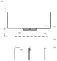
图1展示一种有机发光装置。FIG. 1 shows an organic light emitting device.
图2展示一种不具有分开的电子传递层的倒置式有机发光装置。Figure 2 shows an inverted organic light emitting device without a separate electron transport layer.
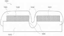
图3展示一种具有多层障壁的例示性装置的横截面。用于无机与聚合物膜两者的沉积掩模的占据空间可以是相同的,在此例示性装置中其比装置占据空间大例如1mm。Figure 3 shows a cross-section of an exemplary device with multilayer barriers. The footprint of the deposition mask for both inorganic and polymeric films can be the same, which in this exemplary device is larger than the device footprint, for example 1 mm.
图4展示一种具有多层障壁的例示性装置的横截面。用于聚合物膜的掩模的占据空间可比装置占据空间大例如1mm,并且无机膜的掩模的占据空间可比聚合物膜的占据空间大例如1mm。Figure 4 shows a cross-section of an exemplary device with multilayer barriers. The footprint of the mask for the polymer film may be larger than the device footprint, for example 1 mm, and the footprint of the mask for the inorganic film may be larger than that of the polymer film, for example 1 mm.
图5展示一种具有多层障壁的例示性装置的横截面。用于无机和聚合物膜的每一堆叠的掩模的占据空间可比前一堆叠大例如1mm。第一堆叠的占据空间比装置的装置占据空间大例如1mm。5 shows a cross-section of an exemplary device with multilayer barriers. The mask footprint for each stack of inorganic and polymer films may be larger than the previous stack, for example by 1mm. The footprint of the first stack is, for example, 1 mm larger than the device footprint of the device.
图6是在等离子体增强的气相沉积(PECVD)系统中垂直安装在衬底电极上的硅片的照片。Figure 6 is a photograph of a silicon wafer mounted vertically on a substrate electrode in a plasma enhanced vapor deposition (PECVD) system.
图7是根据一些实施例的例示性等离子体增强的化学气相沉积设备的横截面图。Figure 7 is a cross-sectional view of an exemplary plasma enhanced chemical vapor deposition apparatus according to some embodiments.
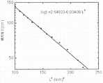
图8是膜厚度的半对数标度(log(t))与长度关系的实验结果的例示性图,其中“长度”对应于在例示性气相沉积工艺中从RF电极到衬底的距离。8 is an exemplary graph of experimental results on a semi-logarithmic scale (log(t)) of film thickness versus length, where "length" corresponds to the distance from the RF electrode to the substrate in an exemplary vapor deposition process.
图9是根据一些实施例的例示性装置的横截面图。Figure 9 is a cross-sectional view of an exemplary device, according to some embodiments.
图10是根据一些实施例从衬底的第一表面到衬底的第二表面的导电体的例示性配置的图解。10 is an illustration of an exemplary configuration of electrical conductors from a first surface of a substrate to a second surface of the substrate in accordance with some embodiments.
图11是根据一些实施例从衬底的第一表面到衬底的第二表面的导电体的例示性配置的图解。11 is an illustration of an exemplary configuration of electrical conductors from a first surface of a substrate to a second surface of the substrate in accordance with some embodiments.
图12(a)和(b)展示根据一些实施例的例示性移动装置。Figures 12(a) and (b) show exemplary mobile devices according to some embodiments.
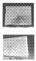
图13包含根据一些实施例在刚刚制作后的实验装置的两个照片。Figure 13 contains two photographs of an experimental setup immediately after fabrication, according to some embodiments.
图14包含根据一些实施例在制作后21小时的来自图13的实验装置的两个照片。Figure 14 contains two photographs of the experimental setup from Figure 13 21 hours after fabrication, according to some embodiments.
图15(a)-(d)展示根据一些实施例的例示性装置和制作工艺。Figures 15(a)-(d) show exemplary devices and fabrication processes according to some embodiments.
图16展示根据一些实施例的例示性装置和制作工艺。Figure 16 shows an exemplary device and fabrication process according to some embodiments.
图17展示根据一些实施例的例示性装置和制作工艺。Figure 17 shows an exemplary device and fabrication process according to some embodiments.
具体实施方式Detailed ways
一般说来,OLED包含至少一个安置在阳极与阴极之间并电连接到阳极和阴极的有机层。当施加电流时,阳极注入空穴并且阴极注入电子到有机层中。注入的空穴和电子各自向带相反电荷的电极迁移。当电子和空穴定位于同一分子时,形成“激子”,激子是具有激发能态的定位的电子-空穴对。当激子通过光发射机制衰减时发出光。在一些情况下,激子可定位于准分子或激发复合物上。例如热弛豫等非辐射机制也可能出现,但一般认为其不合乎需要。In general, an OLED comprises at least one organic layer disposed between and electrically connected to an anode and a cathode. When a current is applied, the anode injects holes and the cathode injects electrons into the organic layer. The injected holes and electrons each migrate toward oppositely charged electrodes. When an electron and a hole are localized in the same molecule, an "exciton" is formed, which is a localized electron-hole pair with an excited energy state. Light is emitted when the excitons decay through a photoemission mechanism. In some cases, excitons can be localized on excimers or exciplexes. Non-radiative mechanisms such as thermal relaxation may also occur, but are generally considered undesirable.
最初OLED使用从单重态发射光(“荧光”)的发射分子,如例如以全文引用的方式并入本文中的美国专利第4,769,292号中所揭示。荧光发射一般发生在不到10纳秒的时间范围内。Originally OLEDs used emissive molecules that emitted light from a singlet state ("fluorescent"), as disclosed, for example, in US Patent No. 4,769,292, which is incorporated herein by reference in its entirety. Fluorescent emission typically occurs on a time scale of less than 10 nanoseconds.
近年来,已经示范具有从三重态发光(“磷光”)的发射材料的OLED。巴多(Baldo)等人,“有机电致发光装置的高效磷光发射(Highly Efficient Phosphorescent Emissionfrom Organic Electroluminescent Devices)”,自然(Nature),第395卷,151-154,1998(“巴多-I”);和巴多(Baldo)等人,“基于电致磷光的极高效绿色有机发光装置(Veryhigh-efficiency green organic light-emitting devices based on electrophosphorescence)”,应用物理通讯(Appl.Phys.Lett.),第75卷,第3期,4-6(1999)(“巴多-II”),其以全文引用的方式并入本文中。磷光在美国专利第7,279,704号第5-6栏中更详细地描述,此专利以引用的方式并入本文中。In recent years, OLEDs with emissive materials that emit light from a triplet state ("phosphorescence") have been demonstrated. Baldo et al., "Highly Efficient Phosphorescent Emission from Organic Electroluminescent Devices", Nature, Vol. 395, 151-154, 1998 ("Baldo-I" ); and Baldo et al., "Very high-efficiency green organic light-emitting devices based on electrophosphorescence," Appl. Phys. Lett. , Vol. 75, No. 3, 4-6 (1999) ("Bardo-II"), which is hereby incorporated by reference in its entirety. Phosphorescence is described in more detail in US Patent No. 7,279,704, columns 5-6, which is incorporated herein by reference.
图1展示一种有机发光装置100。图并不是按比例绘制。装置100可包括衬底110、阳极115、空穴注入层120、空穴传递层125、电子阻挡层130、发射层135、空穴阻挡层140、电子传递层145、电子注入层150、保护层155和阴极160。阴极160是具有第一导电层162和第二导电层164的复合阴极。装置100可通过按顺序沉积所述的层来制作。这么多个层的特性和功能以及实例材料更详细地描述于US7,279,704第6-10栏中,此专利以引用的方式并入本文中。FIG. 1 shows an organic
可获得每一个这些层的更多实例。举例来说,柔性和透明的衬底-阳极组合揭示于美国专利第5,844,363号中,此专利以全文引用的方式併入本文中。p掺杂的空穴传递层的一个实例是以50∶1的摩尔比率掺杂F4-TCNQ的m-MTDATA,如美国专利申请公开案第2003/0230980号中所揭示,此案以全文引用的方式并入本文中。发射和主体材料的实例揭示于汤普森(Thompson)等人的美国专利第6,303,238号中,此专利以全文引用的方式并入本文中。n掺杂的电子传递层的一个实例是以1∶1的摩尔比率掺杂Li的BPhen,如美国专利申请公开案第2003/0230980号中所揭示,此案以全文引用的方式并入本文中。以全文引用的方式并入本文中的美国专利第5,703,436号和第5,707,745号揭示包括复合阴极的阴极的实例,此复合阴极具有例如Mg∶Ag等金属薄层与上覆的透明、导电、经溅镀沉积的ITO层。阻挡层的理论和使用更详细地描述于以全文引用的方式并入本文中的美国专利第6,097,147号和美国专利申请公开案第2003/0230980号中。注入层的实例提供于美国专利申请公开案第2004/0174116号中,此案以全文引用的方式并入本文中。关于保护层的描述可见于美国专利申请公开案第2004/0174116号中,此案以全文引用的方式并入本文中。Further instances of each of these layers are available. For example, flexible and transparent substrate-anode combinations are disclosed in US Patent No. 5,844,363, which is incorporated herein by reference in its entirety. An example of a p-doped hole transport layer is m-MTDATA doped withF4 -TCNQ at a molar ratio of 50:1, as disclosed in U.S. Patent Application Publication No. 2003/0230980, which is incorporated by reference in its entirety way incorporated into this article. Examples of emission and host materials are disclosed in US Patent No. 6,303,238 to Thompson et al., which is incorporated herein by reference in its entirety. An example of an n-doped electron transport layer is BPhen doped with Li at a molar ratio of 1:1, as disclosed in U.S. Patent Application Publication No. 2003/0230980, which is incorporated herein by reference in its entirety . U.S. Patent Nos. 5,703,436 and 5,707,745, which are incorporated herein by reference in their entirety, disclose examples of cathodes comprising composite cathodes having a thin layer of a metal such as Mg:Ag and an overlying transparent, conductive, sputtered The deposited ITO layer is plated. The theory and use of barrier layers is described in more detail in US Patent No. 6,097,147 and US Patent Application Publication No. 2003/0230980, which are hereby incorporated by reference in their entirety. Examples of injection layers are provided in US Patent Application Publication No. 2004/0174116, which is hereby incorporated by reference in its entirety. A description of protective layers can be found in US Patent Application Publication No. 2004/0174116, which is hereby incorporated by reference in its entirety.
图2展示一种倒置式OLED200。所述装置包括衬底210、阴极215、发射层220、空穴传递层225和阳极230。装置200可通过按顺序沉积所述的层来制作。因为最常见的OLED配置在阳极之上安置阴极,并且装置200在阳极230下面安置阴极215,所以装置200可称为“倒置式”OLED。与关于装置100所描述的材料类似的材料可用于装置200的对应层中。图2提供了如何可将某些层从装置100的结构省略掉的一个实例。FIG. 2 shows an
图1和2中说明的简单层状结构是通过非限制性实例提供,并且应了解本发明的实施例可与多种其它结构结合使用。所述的特定材料和结构实际上是例示性的,并且可使用其它材料和结构。功能性的OLED可通过将所述的各层以不同的方式组合来实现,或基于设计、性能和成本因素,可完全省略掉层。也可包括未明确描述的其它层。可使用除明确描述的材料外的材料。尽管本文提供的许多实例描述各层为包含单一材料,但应了解可使用材料组合,例如主体与掺杂剂的混合物,或更一般地混合物。此外,所述层可具有多个子层。本文中给予各层的名称并不意欲严格限制。举例来说,在装置200中,空穴传递层225传递空穴和注入空穴到发射层220中,并且可描述为空穴传递层或空穴注入层。在一个实施例中,OLED可描述为在阴极与阳极之间安置“有机层”。此有机层可包含单个层,或可进一步包含不同有机材料的多个层,如例如关于图1和2所述。The simple layered structures illustrated in Figures 1 and 2 are provided by way of non-limiting example, and it is understood that embodiments of the present invention may be used in conjunction with a variety of other structures. The specific materials and structures described are exemplary in nature, and other materials and structures may be used. Functional OLEDs can be achieved by combining the layers described in different ways, or layers can be omitted entirely based on design, performance and cost factors. Other layers not explicitly described may also be included. Materials other than those explicitly described may be used. Although many of the examples provided herein describe the layers as comprising a single material, it is understood that combinations of materials can be used, such as mixtures of hosts and dopants, or more generally mixtures. Furthermore, the layer may have multiple sublayers. The names given to the various layers herein are not intended to be strictly limiting. For example, in
也可以使用未明确描述的结构和材料,例如包含聚合物材料的OLED(PLED),例如以全文引用的方式并入本文中的弗伦德(Friend)等人的美国专利第5,247,190号中所揭示。通过其它实例,可使用具有单个有机层的OLED。OLED可例如如以全文引用的方式并入本文中的福里斯特(Forrest)等人的美国专利第5,707,745号中所述来堆叠。此OLED结构可与图1和2中说明的简单层状结构不同。举例来说,衬底可包括成角的反射表面以提高出光率(out-coupling),例如如福里斯特(Forrest)等人的美国专利第6,091,195号中所述的台式结构,和/或如布洛维克(Bulovic)等人的美国专利第5,834,893号中所述的坑形结构,这些专利以全文引用的方式并入本文中。Structures and materials not explicitly described may also be used, such as OLEDs (PLEDs) comprising polymeric materials, such as disclosed in U.S. Patent No. 5,247,190 to Friend et al., which is incorporated herein by reference in its entirety. . By way of other example, OLEDs with a single organic layer can be used. OLEDs can be stacked, for example, as described in US Patent No. 5,707,745 to Forrest et al., which is hereby incorporated by reference in its entirety. This OLED structure can differ from the simple layered structure illustrated in FIGS. 1 and 2 . For example, the substrate may include angled reflective surfaces to enhance out-coupling, such as a mesa structure as described in U.S. Patent No. 6,091,195 to Forrest et al., and/or as described in Crater structures described in US Patent No. 5,834,893 to Bulovic et al., which are incorporated herein by reference in their entirety.
除非另外说明,否则各实施例的任一层都可通过任何适合的方法沉积。对于有机层,优选方法包括热蒸发、喷墨(例如在美国专利第6,013,982号和第6,087,196号中描述,这些专利以全文引用的方式并入本文中)、有机气相沉积(OVPD)(例如在福里斯特(Forrest)等人的美国专利第6,337,102号中描述,此专利以全文引用的方式并入本文中)和通过有机气相喷印(OVJP)沉积(例如在美国专利申请案第10/233,470号中描述,此专利以全文引用的方式并入本文中)。其它适合的沉积方法包括旋涂和其它基于溶液的工艺。基于溶液的工艺优选在氮气或惰性氛围中进行。对于其它层,优选方法包括热蒸发。优选图案化方法包括通过掩模沉积、冷焊(例如在美国专利第6,294,398号和第6,468,819号中描述,这些专利以全文引用的方式并入本文中)和与例如喷墨和OVJP等一些沉积方法有关的图案化。也可以使用其它方法。有待沉积的材料可改性以使其与具体的沉积方法相容。举例来说,例如烷基和芳基等分支链或无支链并且优选地包含至少3个碳的取代基可用于小分子中以增强其进行溶液加工的能力。可使用具有20个碳或20个碳以上的取代基,并且3-20个碳是优选范围。具有不对称结构的材料的溶液可加工性可比具有对称结构的材料更好,因为不对称材料可具有较低的再结晶倾向。树枝状聚合物取代基可用于增强小分子进行溶液加工的能力。Unless otherwise stated, any layer of the various embodiments may be deposited by any suitable method. For organic layers, preferred methods include thermal evaporation, inkjet (such as described in U.S. Pat. No. 6,337,102 to Forrest et al., which is incorporated herein by reference in its entirety) and deposition by organic vapor jet printing (OVJP) (such as in U.S. Patent Application No. 10/233,470 described in, which is incorporated herein by reference in its entirety). Other suitable deposition methods include spin coating and other solution based processes. Solution-based processes are preferably performed under nitrogen or an inert atmosphere. For other layers, preferred methods include thermal evaporation. Preferred patterning methods include deposition through a mask, cold welding (such as described in U.S. Pat. related patterning. Other methods can also be used. The material to be deposited can be modified to make it compatible with a particular deposition method. For example, substituents such as alkyl and aryl, branched or unbranched and preferably containing at least 3 carbons, may be used in small molecules to enhance their ability to undergo solution processing. Substituents having 20 carbons or more may be used, and 3-20 carbons is a preferred range. Solution processability of materials with asymmetric structures may be better than materials with symmetric structures because asymmetric materials may have a lower tendency to recrystallize. Dendrimer substituents can be used to enhance the ability of small molecules to undergo solution processing.
根据本发明的实施例制作的装置可并入多种消费品中,包括平板显示器、计算机监测器、电视、广告牌、用于内部或外部照明和/或发信号的光、抬头显示器、完全透明显示器、柔性显示器、激光打印机、电话、手机、个人数字助理(PDA)、膝上型计算机、数字式照相机、可携式摄像机、取景器、微型显示器、车辆、大面积墙壁、电影院或体育场屏幕、照明器材或招牌。多种控制机构可用于控制根据本发明制作的装置,包括被动型矩阵和主动型矩阵。许多装置计划在人类舒适的温度范围中,例如18℃到30℃,并且更优选地在室温下(20-25℃)使用。Devices made in accordance with embodiments of the present invention can be incorporated into a variety of consumer products including flat panel displays, computer monitors, televisions, billboards, lights for interior or exterior lighting and/or signaling, heads up displays, fully transparent displays , flexible displays, laser printers, telephones, cell phones, personal digital assistants (PDAs), laptop computers, digital cameras, camcorders, viewfinders, microdisplays, vehicles, large walls, cinema or stadium screens, lighting equipment or signs. A variety of control mechanisms can be used to control devices made in accordance with the present invention, including passive matrices and active matrices. Many devices are intended for use in a temperature range that is comfortable for humans, eg 18°C to 30°C, and more preferably at room temperature (20-25°C).
本文所述的材料和结构可应用于除OLED外的装置中。举例来说,例如有机太阳能电池和有机光检测器等其它光电装置可采用这些材料和结构。更一般地,例如有机晶体管等有机装置可采用这些材料和结构。The materials and structures described herein can be applied in devices other than OLEDs. For example, other optoelectronic devices such as organic solar cells and organic photodetectors may employ these materials and structures. More generally, organic devices such as organic transistors may employ these materials and structures.
术语卤基、卤素、烷基、环烷基、烯基、炔基、芳烷基、杂环基、芳基、芳族基和杂芳基为此项技术已知,并且在以引用的方式并入本文中的US7,279,704第31-32栏中定义。The terms halo, halogen, alkyl, cycloalkyl, alkenyl, alkynyl, aralkyl, heterocyclyl, aryl, aryl and heteroaryl are known in the art and are used by reference Incorporated herein are the definitions in columns 31-32 of US 7,279,704.
如本文所用,装置的“作用装置区”可指其中产生或吸收电子、空穴和/或光子的装置部分并且可包含一种或一种以上有机和/或半导体材料(例如有机半导体或掺杂硅)。对于有机电子装置,作用装置区可包含一个或一个以上有机层。举例来说,OLED的作用装置区可指装置的发射区(即发光的装置部分)并且可包括有机电致发光材料。太阳能电池的作用装置区可指其中吸收光子并且释放电子的装置部分(例如其可指包含半导体材料的装置部分)。对于薄膜电池,作用装置区可指电解质并且可包含例如锂磷氧氮化物。这些仅仅是例示性装置的作用装置区的几个实例,并且应了解本文所揭示的实施例不受此限制。As used herein, an "active device region" of a device may refer to the portion of the device where electrons, holes, and/or photons are generated or absorbed and may comprise one or more organic and/or semiconducting materials (e.g., organic semiconductors or doped silicon). For organic electronic devices, the active device region may comprise one or more organic layers. For example, the active device region of an OLED can refer to the emissive region of the device (ie, the portion of the device that emits light) and can include an organic electroluminescent material. The active device region of a solar cell may refer to the portion of the device where photons are absorbed and electrons are released (eg, it may refer to the portion of the device comprising semiconductor material). For thin film batteries, the active device region may refer to the electrolyte and may contain, for example, lithium phosphorus oxynitride. These are just a few examples of active device regions of exemplary devices, and it should be understood that the embodiments disclosed herein are not so limited.
如本文所用,术语“约”可指加或减10百分比(包括端点在内)。因此,可了解短语“约10mm”意指9mm到11mm(包括端点在内)。As used herein, the term "about" can mean plus or minus 10 percent, inclusive. Thus, the phrase "about 10 mm" will be understood to mean 9 mm to 11 mm inclusive.
如本文所用,“障壁膜”或“障壁层”可指可用于减少气体、蒸气和/或湿气(或其它环境微粒)渗透到装置的作用装置区中以便延长使用寿命和/或减少性能降级的材料层。在一些实施例中,障壁膜可包含混合层,所述混合层包含聚合物材料与非聚合物材料的混合物。如本文所用,术语“非聚合物”是指由具有定义明确的化学式以及定义明确的单一分子量的分子制成的材料。“非聚合物”分子可具有相当大的分子量。在一些情况下,非聚合物分子可包括重复单元。如本文所用,术语“聚合物”是指由具有共价键联的重复亚单元的分子制成的材料,并且其分子量可随各分子而变化,因为对于每个分子,聚合反应可产生不同数目的重复单元。举例来说,在一些实施例中,障壁膜可包含聚合硅与无机硅的混合物。障壁膜的实例更详细地描述于下文中。As used herein, "barrier film" or "barrier layer" may refer to a film that can be used to reduce the penetration of gas, vapor and/or moisture (or other environmental particles) into the active device area of the device in order to prolong the service life and/or reduce performance degradation. material layer. In some embodiments, the barrier film can include a hybrid layer that includes a mixture of polymeric and non-polymeric materials. As used herein, the term "non-polymer" refers to a material made of molecules having a well-defined chemical formula and a single well-defined molecular weight. A "non-polymeric" molecule can have a relatively large molecular weight. In some cases, non-polymeric molecules may include repeating units. As used herein, the term "polymer" refers to a material made of molecules with covalently linked repeating subunits, and its molecular weight can vary from molecule to molecule because polymerization reactions can produce different numbers of repeating unit. For example, in some embodiments, the barrier film may comprise a mixture of polymeric silicon and inorganic silicon. Examples of barrier films are described in more detail below.
如本文所用,装置的“边界区”(即死角)可包含“非作用装置区”与“非装置边缘区”的组合。如此上下文中所用,边界区的“厚度”可指在垂直于装置占据空间的侧面的方向上从装置占据空间到边界区边缘(在一些实施例中其也可包含衬底边缘)的距离。As used herein, a "boundary region" (ie, dead space) of a device may include a combination of "non-active device region" and "non-device edge region." As used in this context, the "thickness" of a border region may refer to the distance from the device footprint to the edge of the border region (which may also include the edge of the substrate in some embodiments) in a direction perpendicular to the sides of the device footprint.
如本文所用,术语“包含”不意欲是限制性的,而可以是与“包括”、“含有”或“特征是”同义的过渡性术语。由此,术语“包含”可以是包容性或开放性的,并且当用于权利要求时不排除额外未叙述的元件或方法步骤。举例说来,在描述方法时,“包含”表明所述权利要求是开放性的并且允许额外的步骤。在描述装置时,“包含”可意指所指定的元件可对一个实施例是不可缺少的,但其它元件可添加并且仍然形成在权利要求范围内的构造体。相比之下,过渡性短语“由...组成”排除权利要求中未说明的任何元件、步骤或成分。此与此术语在本说明书中的使用一致。As used herein, the term "comprising" is not intended to be limiting, but may be a transitional term that is synonymous with "comprises," "comprising," or "characterized by." Thus, the term "comprising" can be inclusive or open-ended, and when used in a claim does not exclude additional unrecited elements or method steps. For example, when describing a method, "comprising" indicates that the claim is open-ended and allows additional steps. When describing a device, "comprising" may mean that a specified element may be essential to an embodiment, but other elements may be added and still form a construct within the scope of the claims. In contrast, the transitional phrase "consisting of" excludes any element, step or composition not stated in a claim. This is consistent with the use of this term in this specification.
如本文所用,“装置”可包含可沉积(作为单个层或多个层)在衬底之上并且基于电压、电流或光子暴露(例如太阳能电池)的施加可提供所希望的功能性的任何组件。所述装置可包含“作用装置区”(其中产生或吸收电子、空穴和/或光子)和“非作用装置区”。关于出于说明目的的有机装置,“装置”可指一个或一个以上有机层、一个或一个以上绝缘栅格层、电极和如图1和2的实例中所示安置在电极之间的任何层。装置的一个实例是OLED。如本文所用,装置不包括一个或一个以上电接触,其可能远离作用装置区和非作用装置区延伸。也就是说,例如,延伸到不安置在装置占据空间内的一个或一个以上电极的任何部分不构成装置的一部分(例如这些部分可形成电接触)。As used herein, a "device" can include any component that can be deposited (as a single layer or multiple layers) on a substrate and that can provide a desired functionality based on the application of voltage, current, or photon exposure (such as a solar cell) . The device may comprise an "active device region" (in which electrons, holes and/or photons are generated or absorbed) and a "non-active device region". With respect to organic devices for purposes of illustration, "device" may refer to one or more organic layers, one or more insulating grid layers, electrodes, and any layers disposed between the electrodes as shown in the examples of Figures 1 and 2 . One example of a device is an OLED. As used herein, a device does not include one or more electrical contacts, which may extend away from active and non-active device regions. That is, for example, any portions of one or more electrodes that extend to one or more electrodes that are not disposed within the device footprint do not form part of the device (eg, such portions may form electrical contacts).
如本文所用,“装置占据空间”可指装置的“作用装置区”与装置的“非作用装置区”的总面积。关于出于说明目的的有机装置,装置占据空间可指其中一个或一个以上有机层(即有机占据空间)和/或一个或一个以上绝缘栅格层安置在衬底之上的装置部分。As used herein, "device footprint" may refer to the total area of the "active device region" and the "non-active device region" of the device. With respect to organic devices for purposes of illustration, a device footprint may refer to the portion of the device in which one or more organic layers (ie, the organic footprint) and/or one or more insulating grid layers are disposed over a substrate.
如本文所用,装置的“非作用装置区”可指包含一个或一个以上也包括在作用区内的材料层(例如有机层),但不包含其中产生或吸收电子、空穴和/或光子的装置的一部分的装置部分。举例来说,关于OLED,非作用装置区可包括一个或一个以上有机层和/或一部分电极,但装置的此部分可不包括一个或一个以上其它有机层(或一个或一个以上电极),因此不发光。非作用装置区经常(但不是始终)是将有机层沉积,使得延伸到一个电极的边缘以外,从而防止或降低短路的可能性的结果。在一些情况下,绝缘层(例如“栅格层”)可安置在衬底和一部分电极之上,以便使装置的导电层电绝缘。这些区域一般不发光,因此将包含一部分“非作用装置区”。大多数情况下,装置的非作用装置区邻接于作用装置区的一个或一个以上侧面安置。然而,实施例不受此限制并且在一些情况下,装置可具有安置在作用装置区之间的非作用装置区(例如AMOLED显示器可具有在像素之间的可包含“非作用装置区”的非发射区域)。As used herein, an "inactive device region" of a device may refer to a device comprising one or more layers of material (e.g., an organic layer) that is also included in the active region, but does not contain a region in which electrons, holes, and/or photons are generated or absorbed. A device part that is part of a device. For example, with respect to OLEDs, an inactive device region may include one or more organic layers and/or a portion of an electrode, but this portion of the device may not include one or more other organic layers (or one or more electrodes), and therefore not glow. The non-active device region is often, but not always, the result of depositing the organic layer so as to extend beyond the edge of one electrode, thereby preventing or reducing the likelihood of shorting. In some cases, an insulating layer (eg, a "grid layer") may be disposed over the substrate and a portion of the electrodes in order to electrically isolate the conductive layers of the device. These regions generally do not emit light and thus will comprise a portion of the "non-active device region". In most cases, the inactive device region of the device is positioned adjacent to one or more sides of the active device region. However, embodiments are not so limited and in some cases a device may have inactive device regions disposed between active device regions (for example an AMOLED display may have inactive device regions between pixels which may include "inactive device regions"). launch area).
如本文所用,“非装置边缘区”可指在装置占据空间周围的区域,也就是说,不包括装置的“作用装置区”或“非作用装置区”的制品部分。举例来说,非装置边缘区可不包含一个或一个以上属于装置的作用装置区的层。关于有机电子装置,非装置边缘区可指通常不包含有机层或绝缘层(例如安置在OLED的一个电极之上的栅格层)的制品部分。举例说来,非装置边缘区可指不包含例如非作用装置区的一部分的OLED非发射区域。非装置边缘区可包括其中一个或一个以上障壁膜或层沿装置占据空间的侧面安置的制品部分。As used herein, "non-device edge region" may refer to the area surrounding the device footprint, that is, the portion of an article that does not include the "active device region" or "inactive device region" of the device. For example, a non-device edge region may not include one or more layers belonging to the active device region of the device. With respect to organic electronic devices, a non-device edge region may refer to a portion of an article that generally does not contain organic or insulating layers, such as a grid layer disposed over one electrode of an OLED. For example, a non-device edge region may refer to an OLED non-emitting region that does not include, for example, a portion of a non-active device region. The non-device edge region may include the portion of the article in which one or more barrier films or layers are disposed along the sides of the device footprint.
如本文所用,障壁膜的“垂直长度”可指在垂直于装置占据空间的侧面并且平行于上方安置有装置的衬底表面的方向上,从最靠近装置占据空间安置的障壁膜的一部分(例如在一些情况下邻接于作用装置区或非作用装置区)到最远离装置占据空间安置的障壁膜的另一部分(例如障壁膜的边缘)的距离。换句话说,垂直长度可以是障壁膜延伸远离装置占据空间的距离的量度。利用装置占据空间的“侧面”测定垂直长度的理由是一般地排除隅角效应,其中障壁膜的长度可因装置占据空间的形状而变化。因此,一般说来,垂直长度可对应于所安置的障壁膜的长度,以便抵制湿气(和其它污染物)水平进入作用装置区中。As used herein, the "vertical length" of a barrier film may refer to the portion of the barrier film disposed closest to the device footprint (e.g. The distance from, in some cases adjacent to an active device region or an inactive device region) to another portion of the barrier film (eg, an edge of the barrier film) disposed furthest from the device footprint. In other words, the vertical length can be a measure of the distance that the barrier film extends away from the space occupied by the device. The reason for using the "side" of the device footprint to determine the vertical length is to generally exclude corner effects where the length of the barrier film can vary due to the shape of the device footprint. Thus, in general, the vertical length may correspond to the length of the barrier film disposed to resist horizontal ingress of moisture (and other contaminants) into the active device region.
如本文所用,所用的术语“制品”是包容性术语,其可包含具有额外组件或组件(例如在上面安置的障壁层)的装置(例如OLED、薄膜电池、太阳能电池等)、多个安置或布置在单个衬底或多个衬底上的装置或单个装置。因此,在一些情况下,“制品”可与“装置”或“电子装置”互换使用。制品可包括消费型装置(如上所定义)。As used herein, the term "article" is used as an inclusive term that may include devices (such as OLEDs, thin film cells, solar cells, etc.), multiple arrangements or A device or a single device disposed on a single substrate or multiple substrates. Thus, "article of manufacture" may be used interchangeably with "device" or "electronic device" in some instances. An article of manufacture may comprise a consumer device (as defined above).
应指出,尽管下文所述的实施例可参考例如OLED等有机装置,但实施例不受此限制。本发明者已经发现,包含如下所述安置作为边缘密封剂的障壁膜可一般用于任何薄膜电子装置中,尤其是可能具有对例如水蒸气等环境渗透物敏感的组件(或多个组件)的电子装置。此外,本发明者已经发现,如本文中主张,用作边缘密封剂的障壁膜的分布和配置可提供装置,其中所述装置可在衬底边缘的3.0mm(优选地不到2.0mm;更优选地不到1.0mm;并且更优选地不到0.1mm)内安置,同时仍然提供足够的装置性能和使用寿命。装置侧面与衬底边缘之间的距离的减小可减小这些装置的非装置的尺寸并且由此可能减小包含如本文所述安置的障壁膜的电子装置的总体尺寸。在一些情况下,装置的作用装置区可在离衬底边缘0.1mm内安置(此可进一步减小任何边界区的外观,无论是由装置的非装置边缘区(例如障壁层)还是非作用装置区(例如栅格层)产生)。It should be noted that although the embodiments described below may refer to organic devices such as OLEDs, the embodiments are not limited thereto. The present inventors have discovered that a barrier film comprising an edge sealant disposed as described below can be used in general in any thin film electronic device, especially one that may have a component (or components) that are sensitive to environmental permeants such as water vapor. electronic device. Furthermore, the present inventors have discovered that, as claimed herein, the distribution and configuration of a barrier film used as an edge sealant can provide a device where the device can be within 3.0 mm (preferably less than 2.0 mm; more Preferably less than 1.0 mm; and more preferably less than 0.1 mm), while still providing adequate device performance and service life. The reduction in the distance between the sides of the devices and the edge of the substrate can reduce the non-device size of these devices and thus potentially reduce the overall size of an electronic device that includes a barrier film positioned as described herein. In some cases, the active device region of the device can be positioned within 0.1 mm of the substrate edge (this can further reduce the appearance of any border regions, whether by non-device edge regions of the device (such as barrier layers) or non-active device regions. region (e.g. raster layer) generated).
应指出,尽管下文所述的实施例可参考例如OLED等有机装置,但实施例不受此限制。本发明者已经发现,如本文所提供的障壁膜可一般用于任何薄膜电子装置中,尤其是可具有对例如水蒸气等环境渗透物敏感的组件(或组件)的电子装置。此外,本发明者已经发现,例示性障壁膜使装置能够在衬底边缘的3.0mm内(优选地2.0mm内;更优选地1.0mm内)安置,同时仍然提供足够的装置性能和使用寿命。It should be noted that although the embodiments described below may refer to organic devices such as OLEDs, the embodiments are not limited thereto. The inventors have discovered that barrier films as provided herein can be used in any thin film electronic device in general, especially electronic devices that may have components (or components) that are sensitive to environmental permeants such as water vapor. Furthermore, the inventors have discovered that exemplary barrier films enable device placement within 3.0 mm (preferably within 2.0 mm; more preferably within 1.0 mm) of the substrate edge while still providing adequate device performance and lifetime.
一般说来,具有易潮的电子组件(例如对水蒸气敏感的电极)的电子装置在存储时可能因为大气条件而降级。降级可呈暗点的形式,这些暗点由水蒸气和氧气垂直穿过薄膜封装(TFE)整体(或穿过嵌入TFE中的颗粒)进入或由水蒸气和氧气水平穿过TFE边缘进入引起。TFE在本文中也可称为障壁层或障壁膜。水蒸气的边缘进入通常通过渗透物(例如水蒸气分子)水平渗透穿过TFE自身(参见例如图6,下文所述的604),或通过渗透物水平渗透穿过TFE与下伏衬底的界面(参见例如图6,下文所述的605)发生。由此本发明者发现优选地,为电子装置提供边缘密封的TFE减少两种类型的水平渗透(即跨越层自身的渗透和在层与衬底之间的界面处的渗透)。在这点上,本文提供的实施例包含边缘密封,此边缘密封可提供改良的性能并且可用于对例如湿气等大气条件可能敏感的电子装置。In general, electronic devices with moisture-prone electronic components (eg, water vapor-sensitive electrodes) may degrade due to atmospheric conditions when stored. Degradation can be in the form of dark spots caused by the ingress of water vapor and oxygen vertically through the bulk of the thin film encapsulation (TFE) (or through particles embedded in the TFE) or horizontally across the edges of the TFE. TFE may also be referred to herein as a barrier layer or barrier film. Edge entry of water vapor is typically through horizontal permeation of the permeate (e.g. water vapor molecules) through the TFE itself (see e.g. Figure 6, 604 described below), or through the interface of the TFE with the underlying substrate (see eg Figure 6, 605 described below) occurs. The inventors thus found that preferably, TFEs that provide edge seals for electronic devices reduce both types of horizontal permeation (ie permeation across the layer itself and permeation at the interface between the layer and the substrate). In this regard, embodiments provided herein include edge seals that may provide improved performance and may be used in electronic devices that may be sensitive to atmospheric conditions such as moisture.
先前广泛使用的边缘密封利用多层障壁。举例来说,许多装置包含由无机膜与聚合物膜的交替层组成的多层障壁。这些障壁根据通过形成长而弯曲的扩散通路来拖延渗透分子到达装置的原理工作。这些多层障壁的一些实例将在下文描述。Previously widely used edge seals utilized multi-layer barriers. For example, many devices include multilayer barriers consisting of alternating layers of inorganic and polymeric films. These barriers work on the principle of delaying permeate molecules from reaching the device by forming long, tortuous diffusion pathways. Some examples of these multilayer barriers are described below.
用于封装具有多层障壁的装置的先前方法之一是对无机膜与聚合物膜利用相同的掩模;然而,掩模的尺寸大于装置的占据空间,以便提供一些边缘进入障壁(并且也允许掩模对准公差)。假设装置掩模(例如可用于沉积作用装置区、非作用装置区和/或例如电极等其它组件的层的掩模)与封装掩模(例如用于沉积无机膜与聚合物膜的掩模)两者的对准公差是500μm(此对大部分制作工艺来说是合理的),那么此表示封装掩模应比装置掩模大到约1.0mm,以便当在最坏情况下装置的沉积与封装掩模的对准两者都中断时防止任何装置暴露。也可假设多层障壁的无机膜的厚度为约50nm,并且多层障壁的聚合物膜的厚度为约800nm,这些装置通常就是这样。图3提供此类装置的一个实例。One of the previous methods for encapsulating devices with multilayer barriers has utilized the same mask for the inorganic and polymer films; however, the size of the mask is larger than the footprint of the device in order to provide some edge access to the barrier (and also to allow mask alignment tolerance). Assuming device masks (e.g., masks that can be used to deposit layers of active device regions, inactive device regions, and/or other components such as electrodes) and packaging masks (e.g., masks for depositing inorganic and polymeric films) The alignment tolerance of the two is 500μm (which is reasonable for most manufacturing processes), then this means that the package mask should be larger than the device mask by about 1.0mm, so that when the device is deposited with the worst case Both breaks in the alignment of the package mask prevent any device from being exposed. It can also be assumed that the thickness of the inorganic film of the multilayer barrier is about 50 nm, and the thickness of the polymer film of the multilayer barrier is about 800 nm, which is usually the case for these devices. Figure 3 provides an example of such a device.
图3展示制品300,其包含衬底310、具有安置在衬底310之上的装置占据空间的装置301(其可包括作用装置区和非作用装置区)以及封装装置301的多个无机层302和聚合物层303。图3的制品300展示一种多层障壁封装工艺,其由5层堆叠组成,所述堆叠包括五个无机层(302),并且四个聚合物层(303)安置在这些有机层之间(即夹在中间)。一般说来,此类型的掩蔽和沉积方法可使制作相对简单,因为其使用最小数目的掩模改变(因此增加用于制作的最小加工时间),即,在将装置301和对应组件沉积在衬底上后,无机层与聚合物层都可通过单个掩模沉积。如图3中所示,此例示性多层障壁为水蒸气提供一条直接通路(即用箭头304展示的通路-1),使其水平跨越聚合物层303行进并且通过仅仅渗透过一个无机层302(即邻接于装置301的装置占据空间安置的无机层)就到达制品300的装置301(例如对环境敏感的电极或有机层)。因此,如图3中所示的此类型多层障壁所提供的边缘密封主要依赖于水蒸气跨越聚合物材料303的渗透速率(其通常高于无机材料的渗透速率)。一般说来,对于例如图3中所示的装置设计等装置设计,为获得适合的装置性能和使用寿命,此类装置将使用比装置301的占据空间大得多的封装层(例如聚合物303和无机层302)占据空间。也就是说,对无机膜302和有机膜303两者使用比装置占据空间大以沉积边缘密封的单个掩模尺寸可能不是提供具有最少量的边界区(即死角)的装置的有效或实用解决方案。此在以下提供的实例中进一步说明。3 shows an article 300 comprising a substrate 310, a device 301 having a device footprint disposed over the substrate 310 (which may include active and inactive device regions), and a plurality of inorganic layers 302 encapsulating the device 301 and polymer layer 303 . The article 300 of FIG. 3 shows a multilayer barrier encapsulation process consisting of a 5-layer stack comprising five inorganic layers (302) and four polymer layers (303) disposed between these organic layers ( i.e. caught in the middle). In general, this type of masking and deposition method can make fabrication relatively simple because it uses a minimum number of mask changes (thus increasing the minimum process time for fabrication), i.e., after depositing the device 301 and corresponding components on the substrate After topping, both inorganic and polymer layers can be deposited through a single mask. As shown in FIG. 3, this exemplary multilayer barrier provides a direct path for water vapor (i.e., path-1 shown with arrow 304) to travel horizontally across the polymer layer 303 and pass through only one inorganic layer 302. (ie inorganic layers disposed adjacent to the device occupying space of device 301 ) to device 301 of article 300 (eg environmentally sensitive electrodes or organic layers). Thus, the edge seal provided by this type of multilayer barrier as shown in FIG. 3 is primarily dependent on the rate of permeation of water vapor across the polymeric material 303 (which is typically higher than that of inorganic materials). In general, for device designs such as that shown in FIG. 3 , such devices will use encapsulation layers (e.g., polymer 303 and inorganic layer 302) occupy space. That is, using a single mask size for both the inorganic film 302 and the organic film 303 that is larger than the device footprint to deposit edge seals may not be an effective or practical solution for providing a device with a minimal amount of border area (i.e., dead space) . This is further illustrated in the examples provided below.
25℃下水蒸气于聚丙烯酸酯聚合物(一种通常使用的封装材料)中的扩散常数值可通过以下来计算:使用如通过格拉夫(G.L.Graff),威利福德(R.E.Williford)和布罗斯(P.E.Burrows),蒸气渗透穿过多层障壁膜的机制:滞后时间对比平衡渗透(Mechanisms ofvapor permeation through multilayer barrier films:Lag time versus equilibrium permeation),应用物理杂志(J.Appl.Phys.),96(4),第1840-1849页(2004)计算的聚丙烯酸酯聚合物在38℃下的扩散常数(“D”)(即在38℃下的扩散常数(D)为约8.5×10⁻⁹cm2/sec)(此文献以全文引用的方式并入本文中),并且利用如通过陈(Z.Chen),顾(Q.Gu),邹(H.Zou),赵(T.Zhao),王(H.WANG),无定形聚丙烯酸酯胶乳膜内水扩散的分子动力学模拟(Molecular Dynamics Simulation of Water Diffusion InsideanAmorphous PolyacrylateLatex Film),聚合物科学杂志:部分B:聚合物物理学(Journal of Polymer Science:Part B:Polymer Physics),第45卷,884-891(2007)计算的水蒸气在此类聚合物中的活化能(发现近似等于13千焦/摩尔)(此文献也以全文引用的方式并入本文中)。以此方式,25℃下水蒸气于聚丙烯酸酯聚合物中的扩散常数可估计为约6.8×10-9cm2/sec。使用此扩散常数,可估计图3中所示的装置300的水蒸气扩散直通通路-1(304)的滞后时间。如此上下文中所用,滞后时间(tl)是指渗透分子(例如水蒸气分子)跨越距离(l)的近似扩散时间,并且通过以下给出的关系式与材料的扩散常数相关:tl=l2/(6D),如通过格拉夫(Graff)等人,蒸气渗透穿过多层障壁膜的机制:滞后时间对比平衡渗透(Mechanisms of vapor permeationthrough multilayer barrier films:Lag time versus equilibrium permeation),应用物理杂志(J.Appl.Phys.),96(4),第1840-1849页(2004)所示。使用以上计算的水蒸气于聚丙烯酸酯聚合物中的扩散常数(D),可算出对于1.0mm的通路长度,在25℃下的滞后时间接近70小时。也就是说,对于图3中所示的例示性封装方法,当沿通路-1(304)水平行进时,水蒸气一般在室温下将要花费约70小时才能到达邻接于制品300的装置301的占据空间的无机层302。一旦渗透物沿通路-1(304)跨越聚合物层303,则其只需要仅仅渗透过单个无机膜层302(其通常具有约50nm的厚度)就能到达装置301的占据空间。渗透物接着可穿过缺陷(例如针孔、裂缝、粒子等)快速到达作用装置区并且造成破坏。当然,此设计可能引起装置降级,这对所预订的目的或应用来说是不可接受的。The value of the diffusion constant of water vapor in polyacrylate polymers (a commonly used encapsulation material) at 25°C can be calculated by using, for example, by GL Graff, RE Williford and PE Burrows ), Mechanisms of vapor permeation through multilayer barrier films: lag time versus equilibrium permeation (Mechanisms of vapor permeation through multilayer barrier films: Lag time versus equilibrium permeation), Journal of Applied Physics (J.Appl.Phys.), 96(4) , pp. 1840-1849 (2004) the calculated diffusion constant ("D") of polyacrylate polymers at 38°C (i.e., the diffusion constant (D) at 38°C is about 8.5×10⁻⁹ cm2 / sec) (this document is incorporated herein by reference in its entirety), and using such as through Chen (Z.Chen), Gu (Q.Gu), Zou (H.Zou), Zhao (T.Zhao), Wang ( H.WANG), Molecular Dynamics Simulation of Water Diffusion Inside an Amorphous PolyacrylateLatex Film, Journal of Polymer Science: Part B: Polymer Physics (Journal of Polymer Science: Part B: Polymer Physics), Vol. 45, 884-891 (2007) calculated the activation energy of water vapor in such polymers (found to be approximately equal to 13 kJ/mol) (this document is also incorporated by reference in its entirety and into this article). In this way, the diffusion constant of water vapor in polyacrylate polymers at 25°C can be estimated to be about 6.8×10⁻⁹ cm2 /sec. Using this diffusion constant, the lag time for the water vapor diffusion thru-1 (304) of the device 300 shown in FIG. 3 can be estimated. As used in this context, lag time (tl ) refers to the approximate diffusion time of a penetrating molecule (e.g., a water vapor molecule) across a distance (l), and is related to the diffusion constant of the material by the relationship given by: tl = l2 /(6D), as by Graff et al., Mechanisms of vapor permeation through multilayer barrier films: Lag time versus equilibrium permeation, Applied Physics Journal (J. Appl. Phys.), 96(4), pp. 1840-1849 (2004). Using the above calculated diffusion constant (D) for water vapor in polyacrylate polymers, the lag time at 25° C. is calculated to be approximately 70 hours for a path length of 1.0 mm. That is, for the exemplary encapsulation method shown in FIG. 3 , when traveling horizontally along Path-1 ( 304 ), it will take about 70 hours for water vapor to reach occupation of device 301 adjacent to article 300 , typically at room temperature. space for the inorganic layer 302 . Once the permeate crosses the polymer layer 303 along pathway-1 (304), it only needs to permeate through only a single inorganic membrane layer 302 (which typically has a thickness of about 50 nm) to reach the footprint of the device 301. The permeate can then pass through defects (eg, pinholes, cracks, particles, etc.) quickly to the active device area and cause damage. Of course, this design may cause degradation of the device which is unacceptable for the intended purpose or application.
使用多层障壁来封装制品的装置的另一方法展示于图4中。制品400包含衬底410、具有安置在衬底410之上的装置占据空间的装置401(其可包含作用装置区和非作用装置区)以及安置在装置401之上的多个无机层402和聚合物层403。如所示,装置400使用无机层掩模(用于沉积无机层402),所述无机层掩模大于聚合物层掩模(用于沉积聚合物层403),使得无机层420覆盖聚合物层403的侧面。如图4中所示,即使是在此方法中,水平进入通路(即用箭头404展示的通路-1)也是水蒸气水平行进并到达制品400的装置401的最容易通路。对于5层堆叠设计,由此方法产生的针对水蒸气(或其它渗透物)渗透的水平进入通路(即通路-1(404))的障壁层等同于双层障壁,其由第一无机层(通常50nm厚并且邻接于装置401的占据空间安置)、第二聚合物层(通常800nm厚)和第三无机层(通常200nm厚,图4中标记为420)组成。因此,如所示,此类型多层障壁设计提供的对水平渗透的抵抗性等同于由两个无机层和安置在中间(例如夹在中间)的聚合物层组成的多层障壁。因此,当垂直进入包含五个无机障壁层402和四个聚合物层403时,水平进入提供更容易的渗透通路,此通路可决定装置401的使用寿命或降级。Another method for encapsulating a device of an article using a multilayer barrier is shown in FIG. 4 .
对制品使用多层障壁设计的又一个方法展示于图5中。制品500包含衬底510、具有安置在衬底510之上的装置占据空间的装置501(其可包含作用装置区和非作用装置区)以及在装置501的占据空间的侧面之上并且沿装置501的占据空间的侧面安置的多个无机层502和聚合物层503。针对连续的聚合物层503和无机层502,使用尺寸逐渐增大的掩模来沉积障壁层。在此方法中,在制品500的边缘区中沿通路-1(用标记为504的箭头展示)水平行进的水蒸气在到达装置501前在其通路中面对整个多层堆叠(不同于上述图3和4中所示的制品)。在这种情况下,包含层502和503的多层障壁向沿通路-l(504)水平跨越障壁整体行进的水蒸气(或其它渗透物)提供的边缘密封等同于多层障壁向垂直跨越障壁整体行进(即沿用箭头507展示的通路-3)的水蒸气提供的密封。Yet another approach to using a multilayer barrier design for an article is shown in FIG. 5 .
然而,即使水平方向上每单元堆叠的聚合物膜的厚度(如图5中所示,通常各为约1.0mm)比垂直方向上的厚度(通常各为0.8μm)大得多,在两个方向上对水蒸气跨越这些层扩散的抵抗性也是非常类似的。理由是,如格拉夫(G.L.Graff)等人,蒸气渗透穿过多层障壁膜的机制:滞后时间对比平衡渗透(Mechanisms of vapor permeation throughmultilayer barrier films:Lag time versus equilibrium permeation),应用物理杂志(J.Appl.Phys.),96(4),第1840-1849页(2004)所述,在滞后时间计算(tl=l2/(6D))中用于计算长度(l)的有效厚度由聚合物膜的厚度或无机膜中缺陷的间距决定。在垂直方向上(即沿通路-3(507)),假设障壁层的渗透特性优良,无机膜的缺陷间距(例如大约几百微米)比聚合物膜厚度大得多。在水平方向(即沿通路-1(504))上,情况相反,也就是说,无机膜的缺陷间距小于聚合物膜厚度。因此,可以合理地假设,使用逐渐增加的掩模尺寸方法制作的制品500的边缘进入(例如通路-1(504))可与所述多层障壁中垂直渗透(即沿通路-3(507))相比。However, even though the thickness of polymer films stacked per unit in the horizontal direction (typically about 1.0 mm each as shown in FIG. The resistance to the diffusion of water vapor across these layers is also very similar in direction. The reason is, as in Graff (GLGraff) et al., Mechanisms of vapor permeation through multilayer barrier films: lag time versus equilibrium permeation (Mechanisms of vapor permeation through multilayer barrier films: Lag time versus equilibrium permeation), Journal of Applied Physics (J. Appl. Phys.), 96(4), pp. 1840-1849 (2004), the effective thickness used to calculate the length (l) in the lag time calculation (tl = l2 /(6D)) is determined by the aggregation The thickness of the physical film or the spacing of the defects in the inorganic film is determined. In the vertical direction (ie, along pathway-3 (507)), the defect pitch (eg, on the order of hundreds of micrometers) of the inorganic film is much larger than the thickness of the polymer film, assuming good permeation properties of the barrier layer. In the horizontal direction (ie, along via-1 (504)), the situation is reversed, that is, the defect pitch of the inorganic film is smaller than the thickness of the polymer film. Therefore, it is reasonable to assume that the edge entry (e.g. via-1 (504)) of the
尽管上文描述两个进入通路,即水平通路-1(504)和垂直通路-3(507),但渗透物还有另一条可能的进入通路(用箭头505展示的通路-2)。通路-2(505)对应于水蒸气沿无机膜与衬底510的界面渗透。然而,即使沿无机膜的通路-2(505)的界面渗透比无机膜中的整体渗透差,但进入通路跨越界面的长度也是相当大的(例如如图5中所示为约5.0mm),此长度通常是一段足够大的距离,致使其成为与沿通路-1(504)的进入相比次之的进入通路(也就是说,在渗透物穿过通路-2(505)到达装置501前,其更可能穿过通路-1(504)到达装置501。与图5中所示的使用逐渐增大的掩模的边缘封装方法有关的问题之一是与在制作期间使用多个掩模改变有关的复杂性,也就是说,在制作工艺期间每当使用新的掩模时,都要求掩模恰当地对准(增加了工艺的时间和费用)。另外,包含多个无机层502和聚合物层503的障壁的垂直长度(例如占据空间)是巨大的(即在每一侧面上比制品500的装置501宽约5.0mm)。由此,此可能增加装置501的占据空间周围的制品非作用边缘区,可能例如相应地增加装置的边界区(即OLED的非发射区),并且也会为容纳多个边界层而不必要地增加制品尺寸。因此,本发明者已经发现,当试图用无机-聚合物多层障壁减少边缘进入问题时,可能需要长的扩散长度,以便拖延水蒸气(或其它渗透物)在水平方向上(例如沿通路-1(504)或通路2(505))沿制品500的边缘渗透。Although two entry pathways are described above, namely horizontal pathway-1 (504) and vertical pathway-3 (507), there is another possible entry pathway for permeate (path-2 shown with arrow 505). Path-2 ( 505 ) corresponds to water vapor permeating along the interface of the inorganic film and the
因此,如上所述,当试图使用无机-聚合物多层障壁作为边缘密封剂时,通常需要提供长的扩散长度,以便拖延水蒸气(或其它微粒)在水平方向上沿制品的边缘跨越障壁层渗透(无论跨越材料整体还是沿界面)。除非这些层若干毫米厚(即远离装置的侧面延伸若干毫米),否则这些多层障壁设计中利用的技术和配置根本无法拖延渗透物的此边缘进入(例如沿水平通路)。然而,使用若干毫米厚的边缘密封会造成制品的非装置边缘区相对大(对应于在装置的一个或一个以上侧面周围形成边缘密封的障壁层)。此非装置边缘区接着可能要求制品的总体尺寸(包括装置占据空间和非作用装置区的总尺寸)实质上大于装置自身,并且可能由此造成性能或外观上的显著缺陷(例如对于发光装置,产生非发射区)。本发明者已经发现使用障壁膜作为具有对渗透物(例如水蒸气)敏感的组件的装置上的边缘密封的技术和配置,其减少或消除了由边缘密封产生的制品非装置边缘区(或当考虑到制造和例如切割公差等其它误差时至少使制品非装置边缘区减到最小),同时还充分保护装置以减少基于渗透物进入装置的作用装置区的降级并延长使用寿命。Therefore, as noted above, when attempting to use an inorganic-polymer multilayer barrier as an edge sealant, it is often necessary to provide a long diffusion length in order to drag water vapor (or other particulates) across the barrier layer in the horizontal direction along the edge of the article. Penetration (whether across the bulk of the material or along interfaces). Unless the layers are several millimeters thick (ie extending several millimeters away from the sides of the device), the techniques and configurations utilized in these multilayer barrier designs simply cannot delay this edge entry of the permeate (for example along horizontal pathways). However, using an edge seal several millimeters thick results in a relatively large non-device edge region of the article (corresponding to the barrier layer forming the edge seal around one or more sides of the device). This non-device edge region, in turn, may require that the overall dimensions of the article (including the overall size of the device footprint and the non-active device region) be substantially larger than the device itself, and may thereby result in significant defects in performance or appearance (e.g., for light-emitting devices, produce a non-emitting region). The present inventors have discovered techniques and configurations for using a barrier film as an edge seal on a device with components sensitive to permeants (such as water vapor) that reduce or eliminate the non-device edge region of the article (or when At least minimizing non-device edge regions of the article taking into account manufacturing and other tolerances such as cutting tolerances), while also adequately protecting the device to reduce degradation based on permeate ingress into the active device region of the device and prolong useful life.
在这点上并且如下文关于图7和8所示和所述,本发明者已经发现,可形成适合的障壁膜层的材料可在垂直表面以及水平表面上生长。障壁膜材料在垂直表面(例如装置的侧面和/或装置的衬底)上安置的能力可以使装置(无论是装置的作用装置区还是非作用装置区)能够延伸达到并且包括衬底的边缘(由此减少或消除了非装置边缘区),因为障壁膜无须在衬底表面上方并且沿装置的侧面安置(例如沿侧面或从装置占据空间延伸)。取而代之,在一些实施例中,障壁膜可沿装置和/或衬底的垂直侧面安置,以便产生近乎在垂直方向上沿装置和衬底(而非水平远离装置)延伸的边缘密封。In this regard and as shown and described below with respect to Figures 7 and 8, the inventors have discovered that materials that form suitable barrier film layers can be grown on vertical as well as horizontal surfaces. The ability of the barrier film material to sit on vertical surfaces such as the sides of the device and/or the substrate of the device can enable the device (whether active or inactive device region of the device) to extend up to and including the edge of the substrate ( Non-device edge regions are thereby reduced or eliminated), since the barrier film need not be disposed above the substrate surface and along the sides of the device (eg, along the sides or extending from the device footprint). Instead, in some embodiments, a barrier film may be disposed along the vertical sides of the device and/or substrate so as to create an edge seal that extends nearly vertically along the device and substrate (rather than horizontally away from the device).
以下提供本发明者进行的实验的描述,这些实验用于测定沿衬底和/或装置的垂直表面(例如作用装置区或非作用装置区的侧面)安置障壁膜的适用性。本发明者首先在等离子体增强的化学气相沉积(PE-CVD)中在衬底电极上垂直安装一片硅片,如图6的照片中所示。此实验中硅片的高度是约1.0cm。接着障壁膜通过沉积包含聚合物材料与非聚合物材料的混合物的混合障壁膜来生长。包含混合材料的障壁层的例示性沉积方法、条件和材料描述于下文以及例如2007年10月31日申请的美国专利第7,968,146号、2007年4月9日申请的美国专利申请案第11/783,361号、2009年5月5日申请的美国专利申请案第12/990,860号和美国临时申请案第61/086,047号中,每一者都以全文引用的方式并入本文中以达成所有的目的。应了解,除非另外说明,否则任何适合的材料都可用于本文提供的实施例中的障壁膜,并且障壁膜一般可通过任何适合的方式沉积,以便形成如本文所述的边缘密封,如所属领域的技术人员在阅读本发明后将理解的。A description of experiments performed by the inventors to determine the suitability of placing barrier films along vertical surfaces of substrates and/or devices (eg, sides of active or inactive device regions) is provided below. The present inventors first mounted a silicon wafer vertically on a substrate electrode in plasma enhanced chemical vapor deposition (PE-CVD), as shown in the photograph of FIG. 6 . The height of the wafer in this experiment was about 1.0 cm. The barrier film is then grown by depositing a hybrid barrier film comprising a mixture of polymeric and non-polymeric materials. Exemplary deposition methods, conditions, and materials for barrier layers comprising mixed materials are described below and, for example, in U.S. Patent No. 7,968,146, filed October 31, 2007, U.S. Patent Application Serial No. 11/783,361, filed April 9, 2007 No., U.S. Patent Application No. 12/990,860, filed May 5, 2009, and U.S. Provisional Application No. 61/086,047, each of which is incorporated herein by reference in its entirety for all purposes. It should be understood that unless otherwise stated, any suitable material may be used for the barrier films in the examples provided herein, and that the barrier films may generally be deposited by any suitable means to form edge seals as described herein, as described in the art Those skilled in the art will understand after reading the present invention.
本发明者还进行了一项实验来测定例示性障壁膜使用现有的沉积技术和设备可能间接沉积在表面(即实质上不垂直或暴露于沉积材料的表面)之上的程度。参考图7,将描述一个例示性制作工艺和设备,本发明者使用其将障壁膜沉积在衬底之上。如先前所指出,任何类型的沉积工艺都可根据本文提供的实施例使用。在此例示性情况下,本发明者使用PE-CVD设备和沉积技术。一般说来,PE-CVD设备(例如图7中所示的设备700)包含设计成含有真空的反应室和连接到反应室以产生和/或维持适当压力的真空泵。可使用N2气罐来提供N2气体以净化设备700。为了操纵气体流量,设备700还可包括各种流量控制机构(例如质量流量控制器、关闭阀和止回阀),这些机构可在人工或自动控制下。可利用前体材料来源提供前体材料(例如呈液体形式的HMDSO或一种或一种以上在下文更详细地描述的材料),其汽化并馈入反应室中。在一些情况下,前体材料可使用例如氩气等载气传递到反应室。反应气体罐提供反应气体(例如氧气),其也馈入反应室(通过进气口705)。前体材料和反应气体流入反应室中,产生反应混合物。反应室内部的压力可进一步调节以达到沉积压力。The inventors also conducted an experiment to determine the extent to which exemplary barrier films might be deposited indirectly on surfaces (ie, surfaces that are not substantially perpendicular or exposed to the deposition material) using existing deposition techniques and equipment. Referring to FIG. 7, an exemplary fabrication process and apparatus used by the inventors to deposit a barrier film on a substrate will be described. As previously noted, any type of deposition process may be used in accordance with the embodiments provided herein. In this exemplary case, the inventors used PE-CVD equipment and deposition techniques. In general, a PE-CVD apparatus, such as
反应室包括安装在电极支座上的衬底电极701和底电极704,这些电极支座可以是导体或绝缘体。电极网703安置在衬底电极701与底电极704之间并且供有RF功率以在反应混合物中产生等离子体条件。由等离子体产生的反应产物沉积到衬底702上。底电极704还显示为具有进气通道705,其中气体可进入反应室。使反应进行一段足够障壁膜层(例如材料(例如下文所述的材料)的混合层或材料的任何其它适合层)沉积在衬底上的时间。一般说来,反应时间将取决于各种因素,例如衬底相对于电极的位置、有待沉积的材料类型(例如障壁膜材料)、反应条件、障壁膜层的所需厚度、前体材料和反应气体。所属领域的技术人员将了解这些条件可以视具体应用而变化和/或调整以实现具有所需特性的沉积膜层。反应时间通常在5秒与5小时之间,但也可以使用更长或更短的时间,视应用而定。The reaction chamber includes a
如图7中所示,在样品衬底702上的沉积位置与此例示性PE-CVD设备700中的供有RF功率的网状电极703之间存在距离(“L”)。当此距离L增加时,更少的自由基到达衬底702,因此沉积速率减小(即衬底702上沉积材料的生长速率)。在进行PE-CVD工艺后,确定衬底每一位置的距离L以及此位置的沉积层的厚度。所述例示性沉积工艺利用包含HMDSO的前驱材料和作为反应气体的氧气。所述例示性沉积工艺的条件详述于下表1中。在整个沉积工艺中,电极和衬底的位置保持不变。这些测试的结果在图8中的图中说明,此图展示膜厚度的半对数标度(log(t))视距离L的平方而定。对于此实例,如图8所示,log(t)随L2线性减小,具有0.00409的负斜率。因此,基于这些结果,本发明者确定,障壁膜可安置在(例如生长在)未进行安置,使得表面直接暴露于等离子体的表面(即没有直接看到或不垂直于等离子体的表面)。因此,本发明者发现,装置(例如装置的作用装置区和/或非作用装置区)可通过在装置和/或衬底的垂直表面上提供层的一部分来充分封装,即使装置延伸在衬底的边缘或边缘附近。As shown in FIG. 7, there is a distance (“L”) between the deposition location on the
表1:图6中硅片上膜沉积的工艺条件。Table 1: Process conditions for film deposition on silicon wafers in Figure 6.
图9展示一个例示性制品900的横截面,其中装置901安置达到衬底910的边缘。如所示,所述例示性制品包含衬底910,其具有第一表面911、第一侧面912和第一边缘913,其中第一表面911与第一侧面912相接;装置901,其安置在衬底910的第一表面911上并具有侧面902;和障壁膜903。如所示,装置901延伸达到衬底910的第一边缘913,使得装置901的侧面902安置在衬底910的第一边缘913之上(或在离边缘913短距离内,例如不到3.0mm)。例示性装置900中的障壁膜903显示为覆盖(例如安置在其之上)衬底910的第一边缘913、衬底910的第一垂直侧面912的一部分和安置在衬底910的边缘913之上(或在边缘913的短距离内)的装置901的侧面902。制品900的装置901的这样一个封装(或在一些情况下为边缘密封)可通过以下来实现:首先装置901在衬底910上沉积(例如生长),接着切割衬底910和/或装置901,接着通过将制品900安装在沉积室中,使得衬底910的边缘不(尽可能多地)被任何类型的掩模覆盖,由此允许障壁膜在障壁膜沉积期间沉积(并且由此生长)在衬底910的垂直侧面和边缘和/或装置901的垂直侧面上来沉积障壁膜903,以便封装装置901。FIG. 9 shows a cross-section of an
在此例示性实施例中,在制品900的边缘区中沿通路-1(用标记为904的箭头展示)水平行进的水蒸气(或其它渗透物)渗透穿过障壁膜903材料整体,到达装置901。因此,如果障壁膜903包含具有足够扩散系数的材料,那么在此位置中障壁膜903远离装置901的侧面延伸的垂直长度(厚度)可以相对较小(例如小于3.0mm;优选地小于1.0mm;并且更优选地小于0.1mm)。本发明者已经发现,对于一些材料(例如一些本文所述的包含聚合物与非聚合物材料的混合物的混合层),障壁膜903的垂直长度可小于0.1mm并且仍然为足够的装置使用寿命提供充足的边缘密封。如上所述,提供障壁膜903以短的垂直长度可允许装置901的侧面(例如侧面902)在衬底910的边缘913的相应距离内(例如在本实例中在0.1mm内)安置。此外,沿通路-2(用标记为905的箭头展示)的进入可沿衬底910的垂直侧面延伸,此进入对应于制品900的边缘区中跨越障壁膜903与衬底910之间的界面扩散。以此方式,通路-2(905)(其通常具有比障壁膜903的整体扩散系数高的扩散系数)可在不增加障壁膜903远离装置901的侧面延伸的垂直长度下延长。也就是说,通过将障壁膜903进一步沿着衬底910的垂直侧面向下安置(例如覆盖更多的衬底910的侧面912),进入通路-2(905)的长度可延伸相应距离。增加进入通路的长度可延长渗透时间并且由此延长装置的使用寿命(至少在环境降级方面)。因此,不同于其中障壁膜903安置在衬底910的第一表面911之上的实施例,在本实例中通路-2(905)可在不会潜在地增加制品的非装置边缘区下延长(此在障壁膜903远离装置901的侧面延伸的垂直长度增加时获得)。障壁膜903可沿衬底910的侧面912延伸到任何适合的距离。本发明者已经发现,在一些实施例中,可为优选的是,包含聚合物与非聚合物材料的混合物的障壁膜903可沿衬底910的侧面912延伸至少0.1mm(优选地至少1.0mm并且更优选地至少3.0mm)。In this exemplary embodiment, water vapor (or other permeate) traveling horizontally in the edge region of
一般说来,本文提供的一些实施例可使电子装置能够减少或消除非装置边缘区。也就是说,实施例可使装置周长的至少一部分(即装置的边缘)与上方安置其的衬底的边缘重叠(或安置在边缘的短距离内)。在一些实施例中,此可通过将障壁膜沉积在装置的顶部与侧面两者上(例如OLED的有机层之上)并且还延伸障壁膜以覆盖衬底的侧面的一部分来实现。应指出,障壁膜可沿衬底的侧面具有一定厚度(即,障壁膜可在远离上面安置有装置的表面的方向上沿着衬底的侧面向下延伸一定距离)。在一些实施例中,也可将额外的材料安置在障壁膜的顶部之上和/或覆盖衬底边缘的障壁膜部分之上。In general, some embodiments provided herein may enable electronic devices to reduce or eliminate non-device edge regions. That is, embodiments may have at least a portion of the perimeter of the device (ie, the edge of the device) overlap (or be positioned within a short distance of) the edge of a substrate over which it is disposed. In some embodiments, this can be achieved by depositing a barrier film on both the top and sides of the device (eg, over the organic layers of an OLED) and also extending the barrier film to cover a portion of the sides of the substrate. Note that the barrier film may have a thickness along the side of the substrate (ie, the barrier film may extend a distance down the side of the substrate in a direction away from the surface on which the device is disposed). In some embodiments, additional material may also be disposed over the top of the barrier film and/or over the portion of the barrier film that covers the edge of the substrate.
除以上指出的一些优点外,另一个优点可通过基于将障壁膜安置在衬底的垂直侧面之上的一些实施例提供。此垂直表面不可以在任何其它沉积工艺步骤期间已经暴露于任何涂布或表面处理(例如当沉积装置或其它组件时,材料不可以也已经沉积到衬底的侧面上),因此障壁膜可与衬底的垂直侧面的表面形成非常致密的高质量界面。此致密的高质量界面由此可减少跨越障壁膜与衬底之间的界面的渗透,有效地延长装置的使用寿命和/或减少装置的降级(或使障壁膜能够沿衬底的侧面延伸更短距离)。In addition to some of the advantages noted above, another advantage may be provided by some embodiments based on disposing a barrier film over the vertical sides of the substrate. This vertical surface must not have been exposed to any coating or surface treatment during any other deposition process steps (e.g. when depositing a device or other component, material must not have also been deposited onto the sides of the substrate), so the barrier film can be separated from the The surfaces of the vertical sides of the substrate form very dense high-quality interfaces. This dense, high-quality interface can thereby reduce permeation across the interface between the barrier film and the substrate, effectively extending device lifetime and/or reducing device degradation (or enabling the barrier film to extend further along the side of the substrate. short distance).
本文提供的实施例一般可使用任何适合的衬底,例如玻璃或柔性衬底,例如金属箔片和塑料。一般优选地,装置和(至少一部分)衬底的垂直侧面具有优良的障壁膜覆盖。某些工艺可用于制作将推动障壁膜的所述行为的装置,其中一些在下文提供。The embodiments provided herein may generally use any suitable substrate, such as glass or flexible substrates such as metal foils and plastics. It is generally preferred that the vertical sides of the device and (at least a portion of) the substrate have good barrier film coverage. Certain processes can be used to fabricate the devices that will drive the described behavior of the barrier film, some of which are provided below.
在一些实施例中,装置的顶侧面可通过放置/层压具有优良障壁特性的材料层来进一步保护。这些材料可包括(仅举例来说)玻璃、金属箔片和/或涂有障壁的塑料(即在一个或一个以上表面上涂有障壁膜的塑性材料,例如包含聚合物与非聚合物材料的混合物的混合层)。此方法在装置的顶表面上存在粒子/污染物时可尤其优选。In some embodiments, the top side of the device may be further protected by placing/laminating a layer of material with superior barrier properties. These materials may include, by way of example only, glass, metal foil, and/or barrier-coated plastic (i.e., a plastic material that has a barrier film on one or more surfaces, such as a mixed layer of the mixture). This approach may be especially preferred where particles/contaminants are present on the top surface of the device.
在一些实施例中,可沿衬底的侧面提供额外的保护。举例来说,可通过装置的侧面周围的障壁膜封装来保护OLED装置的侧面免受湿气和氧气,此障壁膜封装沿衬底的侧面的一部分延伸。第二障壁膜层或其它的封装也可施加于衬底的侧面,以进一步增强装置的渗透特性。此外,如上所指出,其它涂层和材料可施加于障壁膜封装的顶部和/或衬底上障壁膜的侧面,以提供例如机械保护、用于固持(例如耦接)组件到装置或衬底的特殊纹理或其它的有效功能(例如感测)等功能。在一些实施例中,可为优选的是,这些额外的材料也具有优良的渗透特性。举例来说,本发明的封装装置除阳极外宜包括阳极接触,其中阳极与阳极接触中的至少一者不与湿气反应。或者或另外,本发明的封装装置除阴极外可包括阴极接触,其中阴极与阴极接触中的至少一者不与湿气反应。举例来说,阳极与阳极接触中的至少一者可包含ITO、IZO、金属或其组合。或者或另外,阴极与阴极接触中的至少一者可包含ITO、IZO、金属或其组合。In some embodiments, additional protection may be provided along the sides of the substrate. For example, the sides of an OLED device can be protected from moisture and oxygen by a barrier film encapsulation around the sides of the device, which extends along a portion of the side of the substrate. A second barrier film layer or other encapsulation may also be applied to the sides of the substrate to further enhance the permeation properties of the device. In addition, as noted above, other coatings and materials may be applied to the top of the barrier film package and/or the sides of the barrier film on the substrate to provide, for example, mechanical protection, for holding (e.g., coupling) the component to the device or substrate functions such as special textures or other effective functions (such as sensing). In some embodiments, it may be preferred that these additional materials also have good permeability properties. For example, the packaged device of the present invention preferably includes an anode contact in addition to the anode, wherein at least one of the anode and the anode contact is non-reactive with moisture. Alternatively or additionally, the packaged device of the present invention may comprise a cathode contact in addition to the cathode, wherein at least one of the cathode and the cathode contact is non-reactive with moisture. For example, at least one of the anode and the anode contact can comprise ITO, IZO, metal, or combinations thereof. Alternatively or additionally, at least one of the cathode and cathode contact may comprise ITO, IZO, metal, or combinations thereof.
本文提供的可包含薄膜封装装置的实施例可提供以下优点:不仅在装置的三个侧面上不具有非装置边缘区(或具有有限/减少量的非装置边缘区)(如在本发明者制作的下述实验装置中所示),而且这些装置还可以在装置周围的所有四个侧面(四个以上)上都不具有(或具有有限量的)非装置边缘区。在一些这样的实施例中,电接触点可移向装置的中心(即移到作用装置区中)而非安置在边缘上。此将例如允许例如照明面板或显示器等装置容易进行平铺,因为每一装置的作用装置区之间可能没有显著的非作用(即非发射)区。然而,如下更详细地描述,实施例不受此限制并且电接触可沿衬底的一个或一个以上侧面安置。本文提供的一些实施例的又一优点是,可在大尺寸衬底上使用可重复的母线设计,使得装置(例如照明面板)可切割,以便包括单个图案或图案的多个重复,视所需的装置尺寸而定。另一可能优点,尤其对于包含OLED面板的制品来说,是这些制品可使电子机件(例如智能手机、平板或笔记本式计算机、TV等)在机件水平上不具有(或具有最小)非发射区。在包含有限的非装置边缘区的电子机件中,装置的边缘(和/或侧面)可以暴露(但由障壁膜保护)。然而,如上所提及,本文提供的实施例不局限于例如OLED等有机装置,而可包含含有薄膜障壁层的任何装置或组件。一些其它的电子装置包括太阳能电池、薄膜电池和有机电子仪器。Embodiments provided herein that may include thin film encapsulated devices may provide the advantage of not only having no non-device edge regions (or having a limited/reduced amount of non-device edge regions) on three sides of the device (as in the inventors' fabricated shown in the experimental setup below), and these devices can also have no (or a limited amount of) non-device edge regions on all four sides (more than four) around the device. In some such embodiments, the electrical contacts may be moved toward the center of the device (ie, into the active device region) rather than being positioned on the edges. This would, for example, allow for easy tiling of devices such as lighting panels or displays, since there may not be significant inactive (ie non-emitting) regions between active device regions of each device. However, as described in more detail below, embodiments are not so limited and electrical contacts may be disposed along one or more sides of the substrate. Yet another advantage of some embodiments provided herein is that repeatable busbar designs can be used on large-scale substrates such that devices (e.g., lighting panels) can be cut to include a single pattern or multiple repetitions of a pattern, as desired depends on the size of the device. Another possible advantage, especially for articles comprising OLED panels, is that these articles enable electronic devices (e.g., smartphones, tablet or notebook computers, TVs, etc.) launch area. In electronic devices that contain limited non-device edge regions, the edges (and/or sides) of the device may be exposed (but protected by the barrier film). However, as mentioned above, the embodiments provided herein are not limited to organic devices such as OLEDs, but may encompass any device or component that includes a thin film barrier layer. Some other electronic devices include solar cells, thin film batteries, and organic electronics.
如上所述,本文提供的实施例可包含许多类型消费型电子装置(或其组件)。在装置周围包含有限量(或无)非装置边缘区的制品(例如本文所述的实例)能够实现至少在装置周长的一部分周围(在电子装置水平上)不具有框架的消费型电子装置。图12(a)中说明一个实例,其展示一个例示性智能手机设计,此智能手机设计具有延伸到制品边缘的显示器(在显示器的任何侧面周围都未安置非装置边缘区)。在此设计中,手机的所有四个边缘都不具有框架或非装置边缘区。此设计是通过使外壳1201的占据空间不大于显示面板屏幕1202的占据空间来提供,如图12(b)中所说明。在其它设计实施例中,不是消费型电子装置的所有四个侧面都会构成装置的侧面(即可能有一个或一个以上侧面具有延伸在显示器占据空间之外的非装置边缘区和/或框架)。As noted above, the embodiments provided herein may incorporate many types of consumer electronic devices (or components thereof). Articles that include a limited amount (or none) of non-device edge regions around the device, such as the examples described herein, enable consumer electronic devices that do not have a frame around at least a portion of the device perimeter (at the electronics level). An example is illustrated in Figure 12(a), which shows an exemplary smartphone design with a display extending to the edge of the article (with no non-device edge regions disposed around any sides of the display). In this design, all four edges of the phone have no frame or non-device edge areas. This design is provided by making the footprint of the
在一些实施例中,用于制作制品(例如图9中所示的例示性实施例)的方法可包含以下工艺顺序:1)刻划衬底的后表面(即上面未安置装置的衬底表面);2)将装置安置(例如生长)在衬底的前表面(例如与后表面相对的表面)上;3)在预先刻划的位置处使衬底断裂以暴露装置和衬底的垂直侧面;和4)施加障壁膜封装以覆盖装置的侧面(和在一些实施例中是顶部)与衬底的边缘和至少一部分垂直侧面。In some embodiments, a method for fabricating an article (such as the exemplary embodiment shown in FIG. 9 ) may include the following process sequence: 1) Scribing the back surface of the substrate (i.e., the surface of the substrate on which no device is placed) ); 2) placing (e.g., growing) the device on the front surface of the substrate (e.g., the surface opposite the back surface); 3) breaking the substrate at pre-scribed locations to expose the device and the vertical sides of the substrate and 4) applying a barrier film encapsulation to cover the sides (and in some embodiments the top) of the device with the edges and at least a portion of the vertical sides of the substrate.
上述工艺是作为可如何制作这样一种例示性装置的一个实例提供。然而,如上所指出,如所属领域的技术人员在阅读本发明后可理解的,包含覆盖衬底的边缘和侧面的一部分(以及装置的侧面)的障壁膜的实施例可使用任何适合的方法制作。举例来说,本发明者已经发现一些实施例可包含以下任一者:不刻划和/或切割衬底和/或装置,而是可使用小衬底(即具有小表面供装置在上面安置的衬底)。装置的占据空间可大于衬底的表面,导致装置延伸到衬底的边缘。衬底与装置都可暴露垂直侧面,当沉积障壁膜时这些垂直侧面可覆盖。The process described above is provided as an example of how such an exemplary device may be fabricated. However, as noted above, embodiments comprising a barrier film covering a portion of the edges and sides of the substrate (and the sides of the device) may be fabricated using any suitable method, as would be understood by one of ordinary skill in the art after reading this disclosure. . For example, the inventors have discovered that some embodiments may include any of the following: Instead of scoring and/or cutting the substrate and/or devices, small substrates (i.e., having small surfaces for devices to rest on) may be used substrate). The footprint of the device may be larger than the surface of the substrate, resulting in the device extending to the edge of the substrate. Both the substrate and the device can have exposed vertical sides, which can be covered when the barrier film is deposited.
制作制品的另一例示性方法可以是在不预先刻划衬底下安置装置(例如使装置的层生长)。在装置(例如OLED的有机层)沉积后,装置的侧面和衬底的至少一部分侧面可通过以下任一者暴露:刻划到衬底中;对装置和衬底进行激光切削;或任何其它适合的方法。接着可沉积障壁膜,以便覆盖装置的侧面以及衬底的边缘和暴露侧面的至少一部分。在一些实施例中,例如当使用例如金属箔片或塑料等柔性衬底时,将衬底侧面和/或装置侧面暴露的简单方法是使用剪刀切割(或任何其它的切割技术)。接着可沉积障壁膜,以便覆盖装置的侧面以及衬底的边缘和暴露侧面的至少一部分。Another exemplary method of fabricating an article may be to place the device (eg, grow layers of the device) without pre-scribing the substrate. After deposition of the device (such as the organic layers of an OLED), the sides of the device and at least a portion of the sides of the substrate may be exposed by either: scribing into the substrate; laser ablation of the device and substrate; or any other suitable Methods. A barrier film may then be deposited so as to cover the sides of the device and at least a portion of the edges and exposed sides of the substrate. In some embodiments, for example when using flexible substrates such as metal foil or plastic, a simple way to expose the sides of the substrate and/or the sides of the device is to use scissors cutting (or any other cutting technique). A barrier film may then be deposited so as to cover the sides of the device and at least a portion of the edges and exposed sides of the substrate.
电连接electrical connection
如上所述,本文提供的使用薄膜封装的实施例可提供制成具有非常靠近衬底边缘的装置的制品(例如包含OLED显示器的制品)的能力。此可为看作单个显示器或当平铺多个装置以制成更大的显示系统时提供例如真正无边界(或接近无边界)显示器。尽管以下提供的实例将参考显示器来描述,但提供电接触到安置在衬底上的装置的实施例可同等地适用于其它类型的装置,例如本文中作为实例提供的装置类型(例如太阳能电池、薄膜电池、有机电子装置等)。As noted above, embodiments provided herein using thin-film encapsulation can provide the ability to make articles with devices very close to the edge of the substrate, such as articles comprising OLED displays. This can provide, for example, a truly borderless (or nearly borderless) display as a single display or when multiple devices are tiled to make a larger display system. Although the examples provided below will be described with reference to displays, embodiments providing electrical contacts to devices disposed on a substrate are equally applicable to other types of devices, such as the types of devices provided as examples herein (e.g., solar cells, thin film batteries, organic electronic devices, etc.).
例如显示器等这些无边界装置(即在装置的一个或一个以上侧面周围没有或具有减少的非装置边缘区的装置)的一个可能问题是如何向装置提供必要的电力驱动(尤其对于利用行与列信号的显示器)。在常规的显示器中,这些信号可通过使用在衬底上制作的薄膜晶体管(TFT)或通过在显示器边缘附近粘结到衬底的集成电路,利用靠近显示器边缘的连接,在具有或不具有多路传输这些信号、提供扫描驱动器等的综合功能性下来施加于显示器。One possible problem with these borderless devices (i.e., devices with no or reduced non-device edge area around one or more sides of the device), such as displays, is how to provide the necessary power drive to the device (especially for devices utilizing row and column signal display). In a conventional display, these signals can be utilized with connections close to the edge of the display, with or without multiple The comprehensive functionality of transmitting these signals, providing scan drivers, etc. is applied to the display.
下文提供的是两个为真正无边界(或接近无边界)显示器提供电子连接的例示性方法。在每个这些实例中,一般概念是将显示器前面的行和列电极与显示器后面的电连接相连接,以便连接器和驱动电路(例如装置的电子器件封装的部分)可施加于显示器的后表面。以此方式,这些组件将安置在衬底和/或装置的区域(即占据空间)内,并且在装置周围将无需或不会产生非装置边缘区或边界/框架。一般说来,下文提供的例示性方法将优选在底板制作和前板制作前进行,不过实施例可不受此限制。Provided below are two exemplary methods of providing electrical connectivity for truly borderless (or nearly borderless) displays. In each of these instances, the general concept is to connect the row and column electrodes on the front of the display with the electrical connections on the rear of the display so that connectors and drive circuitry (such as part of the electronics package of the device) can be applied to the rear surface of the display . In this way, these components will fit within the area (ie, footprint) of the substrate and/or device, and there will be no need or creation of non-device edge regions or borders/frames around the device. In general, the exemplary methods provided below will preferably be performed prior to backplane fabrication and frontplane fabrication, although embodiments may not be so limited.
第一例示性实施例包含使用在衬底中制作的从衬底的前表面延伸到后表面的通孔。此在图10中说明,其展示衬底1010,所述衬底1010具有前(或顶)表面1011和后(或底)表面1020,并且包含多个微孔1002,这些微孔1002钻穿玻璃(或其它适合的衬底材料)衬底1010。这些通孔(例如微孔1002)可填充有导电材料(例如金属),以提供显示器前表面1011上的行或列线与显示器的后表面1020上的电连接之间的电连接性。微孔1002可靠近显示器边缘1012(如所示)或安置在显示器上的其它任何地方。A first exemplary embodiment involves the use of vias made in the substrate extending from the front surface to the back surface of the substrate. This is illustrated in Figure 10, which shows a
第二例示性实施例包含使安置在显示器侧面上的导体图案化以将显示器前表面上的行和列线与后表面上的电连接相连接。此在图11中说明,其展示衬底1110,所述衬底1110具有前(或顶)表面1111和后(或底)表面1120,并且沿衬底1110的侧面1112包含多个图案化导体1102。图案化的导体1102可沿衬底侧面1112和/或衬底1110的顶表面1111包含导电迹线,其可将显示器的前面1111上的一个或一个以上母线与后面1120上的电连接相连接。图案化的导体1102可使用任何适合的方法形成,例如直接印刷(例如薄的电线从可溶性导电墨水进行喷墨印刷);使用真空沉积工艺,利用阴影掩模,进行沉积和图案化;在显示器侧面1112上沉积金属或导电墨水,接着使用平版印刷术或使用激光图案化以从区域切削膜,以去除导电材料并留下导电迹线或导线,其中沉积工艺可包括通过真空工艺(例如溅镀、蒸发等)沉积金属或导体;或通过将显示器侧面1112浸渍到可溶性导电墨水中。A second exemplary embodiment involves patterning conductors disposed on the sides of the display to connect row and column lines on the front surface of the display with electrical connections on the rear surface. This is illustrated in FIG. 11 , which shows a
在任一种情况下,这些例示性方法都可以允许应用障壁膜来在装置周围封装和形成密封,包括任何或所有图案化的导体。如上所指出,尽管例示性方法是关于显示装置描述,但实施例不受此限制。相同或类似的方法可应用于照明面板或利用障壁膜作为边缘或封装层的任何其它装置。对于大部分装置,尤其是照明面板,图案化的导体的数目通常比对显示器所要求的数目少得多,因此这些方法更容易实施。In either case, these exemplary methods may allow application of a barrier film to encapsulate and form a seal around the device, including any or all patterned conductors. As noted above, although the exemplary method is described with respect to a display device, the embodiments are not so limited. The same or similar approach can be applied to lighting panels or any other device that utilizes a barrier film as an edge or encapsulation layer. For most devices, especially lighting panels, the number of patterned conductors is usually much less than required for displays, so these methods are easier to implement.
例示性障壁膜的组成和制作Composition and Fabrication of Exemplary Barrier Films
以下提供可在如上所述的一些实施例中用作边缘密封剂的障壁膜分子和材料的例示性组合物(和制作这些组合物的方法)。在这点上,可用作边缘密封剂的材料(和沉积工艺)的例示性实施例在标题为“用于电子装置或其它物品上的涂层中的混合层(HybridLayers for Use in Coatings onElectronic Devices or Other Articles)”的美国专利第7,968,146号中详细描述,此专利以全文引用的方式并入本文中以达成所有目的。本发明者已经发现,美国专利第7,968,146号中描述的材料和方法可提供可优选用作电子装置的边缘密封剂的障壁膜,这些材料和方法中的一些提供于下文中。然而,实施例不必限于其中所述的分子和方法。Exemplary compositions of barrier film molecules and materials (and methods of making these compositions) that can be used as edge sealants in some embodiments as described above are provided below. In this regard, illustrative examples of materials (and deposition processes) that may be used as edge sealants are described in the publication entitled "Hybrid Layers for Use in Coatings on Electronic Devices" or Other Articles), which is incorporated herein by reference in its entirety for all purposes. The present inventors have discovered that the materials and methods described in US Patent No. 7,968,146, some of which are provided below, can provide barrier films that can be preferably used as edge sealants for electronic devices. However, the embodiments are not necessarily limited to the molecules and methods described therein.
在这点上并且如上所指出,在一些实施例中,障壁膜可包含含有聚合物材料与非聚合物材料的混合物的混合层。混合层可具有单个相或多个相。In this regard and as noted above, in some embodiments, the barrier film may comprise a hybrid layer comprising a mixture of polymeric and non-polymeric materials. A mixed layer can have a single phase or multiple phases.
如本文所用,术语“非聚合物”可指由具有定义明确的化学式以及定义明确的单一分子量的分子制成的材料。“非聚合物”分子可具有相当大的分子量。在一些情况下,非聚合物分子可包括重复单元。如本文所用,术语“聚合物”可指由具有共价键联的重复亚单元的分子制成的材料,并且其分子量可随各分子而变化,因为对于每个分子,聚合反应可产生不同数目的重复单元。聚合物可包括(但不限于)均聚物和共聚物,例如嵌段、接枝、无规或交替共聚物,以及其掺合物和改性。聚合物包括(但不限于)碳或硅的聚合物。As used herein, the term "non-polymer" may refer to a material made of molecules having a well-defined chemical formula and a well-defined single molecular weight. A "non-polymeric" molecule can have a relatively large molecular weight. In some cases, non-polymeric molecules may include repeating units. As used herein, the term "polymer" may refer to a material made of molecules having covalently linked repeating subunits, and its molecular weight may vary from molecule to molecule because polymerization reactions may produce different numbers of repeating unit. Polymers may include, but are not limited to, homopolymers and copolymers, such as block, graft, random or alternating copolymers, and blends and modifications thereof. Polymers include, but are not limited to, polymers of carbon or silicon.
如本文所用,“聚合物材料与非聚合物材料的混合物”可指所属领域的技术人员所了解的,既不是纯的聚合物,也不是纯的非聚合物的组合物。术语“混合物”意欲排除含有少量非聚合物材料(通常其可以例如存在于聚合物材料的缝隙中),但所属领域的技术人员仍然认为是纯聚合物的任何聚合物材料。同样,此意欲排除含有少量聚合物材料,但所属领域的技术人员仍然认为是纯的非聚合物的任何非聚合物材料。在一些情况下,混合层中聚合物材料与非聚合物材料的重量比在95∶5到5∶95范围内,并且优选地在90∶10到10∶90范围内,并且更优选地在25∶75到10∶90范围内。As used herein, a "mixture of polymeric material and non-polymeric material" may refer to a composition that is neither a pure polymer nor a pure non-polymer, as understood by those skilled in the art. The term "mixture" is intended to exclude any polymeric material that contains small amounts of non-polymeric material (which may normally be present, for example, in interstices of polymeric material), but which would still be considered by a person skilled in the art to be a pure polymer. Again, this is intended to exclude any non-polymeric material that contains small amounts of polymeric material, but would still be considered pure non-polymeric by those skilled in the art. In some cases, the weight ratio of polymeric material to non-polymeric material in the mixed layer is in the range of 95:5 to 5:95, and preferably in the range of 90:10 to 10:90, and more preferably in the range of 25 :75 to 10:90 range.
一层的聚合物/非聚合物组成可使用各种技术确定,包括水滴的润湿接触角、IR吸收、硬度和柔性。在某些情况下,混合层具有在30°到85°范围内,并且优选地在30°到60°范围内,并且更优选地在36°到60°范围内的润湿接触角。注意,如果在如所沉积的膜的表面上测定,那么润湿接触角是组成的尺度。因为润湿接触角通过沉积后处理会极大地变化,所以在这些处理后进行的测量可能无法反映层的组成。相信这些润湿接触角适用于由有机硅前体形成的各类层。在某些情况下,混合层具有在3到20GPa范围内,并且优选地在10到18GPa范围内的纳米压痕硬度。在某些情况下,混合层具有在0.1nm到10nm范围内,并且优选地在0.2nm到0.35nm范围内的表面粗糙度(均方根)。在某些情况下,混合层当在50mm厚的聚酰亚胺箔片衬底上沉积为4mm厚的层时是足够柔性的,以致在0.2%的拉伸应变(ε)下在1英寸直径滚筒上至少55,000个滚轧循环后未观察到微观结构变化。在某些情况下,混合层是足够柔性的,以致在至少0.35%的拉伸应变(ε)(典型地,如所属领域的技术人员所认为的,是通常使4mm纯氧化硅层破裂的拉伸应变水平)下未出现裂缝。The polymer/non-polymer composition of a layer can be determined using various techniques, including wetting contact angle of water droplets, IR absorption, hardness and flexibility. In some cases, the hybrid layer has a wetting contact angle in the range of 30° to 85°, and preferably in the range of 30° to 60°, and more preferably in the range of 36° to 60°. Note that the wetting contact angle is a measure of composition if measured on the surface of the as-deposited film. Because wetting contact angles vary greatly by post-deposition treatments, measurements made after these treatments may not reflect the composition of the layer. These wetting contact angles are believed to apply to all types of layers formed from organosilicon precursors. In some cases, the hybrid layer has a nanoindentation hardness in the range of 3 to 20 GPa, and preferably in the range of 10 to 18 GPa. In some cases, the hybrid layer has a surface roughness (root mean square) in the range of 0.1 nm to 10 nm, and preferably in the range of 0.2 nm to 0.35 nm. In some cases, the hybrid layer was sufficiently flexible when deposited as a 4 mm thick layer on a 50 mm thick polyimide foil substrate that the No microstructural changes were observed after at least 55,000 rolling cycles on the drum. In some cases, the hybrid layer is sufficiently flexible that at a tensile strain (ε) of at least 0.35% (typically, as considered by those skilled in the art, the tensile strain that normally ruptures a 4 mm layer of pure silicon oxide No cracks appeared at the elongation level).
应指出,术语“混合物”意欲包括具有单个相的组合物以及具有多个相的组合物。因此,“混合物”排除随后沉积的交替聚合物与非聚合物层。换句话说,为了视作“混合物”,层应该在相同的反应条件下和/或同时沉积。It should be noted that the term "mixture" is intended to include compositions having a single phase as well as compositions having multiple phases. Thus, "mixture" excludes subsequently deposited alternating polymer and non-polymer layers. In other words, to be considered a "mixture", the layers should be deposited under the same reaction conditions and/or simultaneously.
混合层可通过化学气相沉积,使用单一前体材料(例如来自单个来源或多个来源)形成。如本文所用,“前体材料的单个来源”可指当前体材料在有或无反应气体下通过CVD沉积时,提供形成聚合物与非聚合物材料所需的所有前体材料的来源。此意欲排除其中聚合物材料使用一种前体材料形成,而非聚合物材料使用不同的前体材料形成的方法。如所属领域的技术人员将了解,前体材料的“单个来源”可包括一个或一个以上在工艺期间可用于加热或混合可形成或含有单一前体材料的化学物质的容器(例如坩埚)。举例来说,单一前体材料可混合或位于多个容器中,接着进行气相沉积。一般说来,通过使用单一前体材料,可以简化沉积工艺。举例来说,单一前体材料将避免对前体材料的分开流的需要以及随之对供应和控制分开流的需要。Mixed layers can be formed by chemical vapor deposition using a single precursor material (eg, from a single source or from multiple sources). As used herein, "single source of precursor materials" may refer to a source that provides all of the precursor materials needed to form polymeric and non-polymeric materials when the precursor materials are deposited by CVD with or without reactive gases. This is intended to exclude methods in which the polymeric material is formed using one precursor material and the non-polymeric material is formed using a different precursor material. As will be appreciated by those skilled in the art, a "single source" of precursor material may include one or more vessels (eg, crucibles) that may be used during the process to heat or mix chemicals that may form or contain a single precursor material. For example, a single precursor material may be mixed or located in multiple containers, followed by vapor deposition. In general, the deposition process can be simplified by using a single precursor material. For example, a single precursor material would avoid the need for separate streams of precursor material and the consequent need to supply and control separate streams.
一般说来,前体材料可以是单一化合物或化合物的混合物。在前体材料是化合物的混合物时,在一些情况下,混合物中不同化合物的每一者自身能够独立地充当前体材料。举例来说,前体材料可以是六甲基二硅氧烷(HMDSO)与二甲基硅氧烷(DMSO)的混合物。还可以利用其它前体,例如四乙氧基硅烷(TEOS)或二甲基硅氧烷(DMSO)或八甲基环四硅氧烷或六甲基二硅氮烷或其它的有机硅烷或有机硅氧烷和有机硅氮烷或其混合物。In general, the precursor material can be a single compound or a mixture of compounds. Where the precursor material is a mixture of compounds, in some cases each of the different compounds in the mixture can independently serve as a precursor material by itself. For example, the precursor material may be a mixture of hexamethyldisiloxane (HMDSO) and dimethylsiloxane (DMSO). Other precursors such as tetraethoxysilane (TEOS) or dimethylsiloxane (DMSO) or octamethylcyclotetrasiloxane or hexamethyldisilazane or other organosilanes or organic Silicones and organosilazanes or mixtures thereof.
在一些情况下,等离子体增强的CVD(PE-CVD)可用于沉积混合层。PE-CVD可出于多种原因而为合意的,包括低温沉积、形成均一涂层和可控制的工艺参数。适用于形成可构成用于边缘密封剂的障壁层的混合层的各种PE-CVD工艺为所属领域中已知,包括使用RF能来产生等离子体的PE-CVD工艺。In some cases, plasma enhanced CVD (PE-CVD) can be used to deposit the hybrid layer. PE-CVD may be desirable for a number of reasons, including low temperature deposition, formation of uniform coatings, and controllable process parameters. Various PE-CVD processes suitable for forming hybrid layers that may constitute barrier layers for edge sealants are known in the art, including PE-CVD processes that use RF energy to generate a plasma.
前体材料可以是能够在通过化学气相沉积进行沉积时形成聚合物材料与非聚合物材料两者的材料。各种这样的前体材料适用于提供包含混合层的障壁膜并且可以针对其各种特征进行选择。举例来说,前体材料可以针对其化学元素含量、其化学元素的化学计量比和/或在CVD下形成的聚合物和非聚合物材料来选择。举例来说,例如硅氧烷等有机硅化合物是一类适用作前体材料的化合物。硅氧烷化合物的代表性实例包括六甲基二硅氧烷(HMDSO)和二甲基硅氧烷(DMSO)。当通过CVD沉积时,这些硅氧烷化合物能够形成例如硅酮聚合物等聚合物材料和例如氧化硅等非聚合物材料。前体材料也可以针对各种其它的特征,例如成本、无毒性、操纵特点、在室温下维持液相的能力、挥发性、分子量等进行选择。The precursor material may be a material capable of forming both polymeric and non-polymeric materials when deposited by chemical vapor deposition. A variety of such precursor materials are suitable for providing the barrier film comprising the hybrid layer and can be selected for its various characteristics. For example, the precursor material may be selected for its chemical element content, its stoichiometric ratio of chemical elements, and/or polymer and non-polymer materials formed under CVD. For example, organosilicon compounds such as siloxanes are a class of compounds suitable as precursor materials. Representative examples of silicone compounds include hexamethyldisiloxane (HMDSO) and dimethylsiloxane (DMSO). When deposited by CVD, these siloxane compounds are capable of forming polymeric materials such as silicone polymers and non-polymeric materials such as silicon oxide. Precursor materials can also be selected for various other characteristics, such as cost, non-toxicity, handling characteristics, ability to maintain a liquid phase at room temperature, volatility, molecular weight, and the like.
适用作前体材料的其它有机硅化合物包括甲基硅烷;二甲基硅烷;乙烯基三甲基硅烷;三甲基硅烷;四甲基硅烷;乙基硅烷;二硅烷基甲烷;双(甲基硅烷基)甲烷;1,2-二硅烷基乙烷;1,2-双(甲基硅烷基)乙烷;2,2-二硅烷基丙烷;1,3,5-三硅烷基-2,4,6-三亚甲基,和这些化合物的氟化衍生物。适用作前体材料的含有苯基的有机硅化合物包括:二甲基苯基硅烷和二苯基甲基硅烷。适用作前体材料的含氧有机硅化合物包括:二甲基二甲氧基硅烷;1,3,5,7-四甲基环四硅氧烷;1,3-二甲基二硅氧烷;1,1,3,3-四甲基二硅氧烷;1,3-双(硅烷基亚甲基)二硅氧烷;双(1-甲基二硅氧烷基)甲烷;2,2-双(1-甲基二硅氧烷基)丙烷;2,4,6,8-四甲基环四硅氧烷;八甲基环四硅氧烷;2,4,6,8,10-五甲基环五硅氧烷;1,3,5,7-四硅烷基-2,6-二氧基-4,8-二亚甲基;六甲基环三硅氧烷;1,3,5,7,9-五甲基环五硅氧烷;六甲氧基二硅氧烷,和这些化合物的氟化衍生物。适用作前体材料的含氮有机硅化合物包括:六甲基二硅氮烷;二乙烯基四甲基二硅氮烷;六甲基环三硅氮烷;二甲基双(N-甲基乙酰胺基)硅烷;二甲基双-(N-乙基乙酰胺基)硅烷;甲基乙烯基双(N-甲基乙酰胺基)硅烷;甲基乙烯基双(N丁基乙酰胺基)硅烷;甲基三(N-苯基乙酰胺基)硅烷;乙烯基三(N-乙基乙酰胺基)硅烷;四(N甲基乙酰胺基)硅烷;二苯基双(二乙基胺氧基)硅烷;甲基三(二乙基胺氧基)硅烷;和双(三甲基硅烷基)碳化二亚胺。Other organosilicon compounds suitable as precursor materials include methylsilane; dimethylsilane; vinyltrimethylsilane; trimethylsilane; tetramethylsilane; ethylsilane; silyl)methane; 1,2-disilylethane; 1,2-bis(methylsilyl)ethane; 2,2-disilylpropane; 1,3,5-trisilyl-2, 4,6-trimethylene, and fluorinated derivatives of these compounds. Phenyl-containing organosilicon compounds suitable as precursor materials include: dimethylphenylsilane and diphenylmethylsilane. Oxygen-containing organosilicon compounds suitable as precursor materials include: dimethyldimethoxysilane; 1,3,5,7-tetramethylcyclotetrasiloxane; 1,3-dimethyldisiloxane ; 1,1,3,3-tetramethyldisiloxane; 1,3-bis(silylmethylene)disiloxane; bis(1-methyldisiloxane)methane; 2, 2-bis(1-methyldisiloxane)propane; 2,4,6,8-tetramethylcyclotetrasiloxane; octamethylcyclotetrasiloxane; 2,4,6,8, 10-pentamethylcyclopentasiloxane; 1,3,5,7-tetrasilyl-2,6-dioxy-4,8-dimethylene; hexamethylcyclotrisiloxane; 1 , 3,5,7,9-pentamethylcyclopentasiloxane; hexamethoxydisiloxane, and fluorinated derivatives of these compounds. Nitrogen-containing organosilicon compounds suitable as precursor materials include: hexamethyldisilazane; divinyltetramethyldisilazane; hexamethylcyclotrisilazane; dimethylbis(N-methyl Acetamido)silane; Dimethylbis-(N-ethylacetamido)silane; Methylvinylbis(N-methylacetamido)silane; Methylvinylbis(N-butylacetamido) ) silane; Methyltris(N-phenylacetamido)silane; Vinyltris(N-ethylacetamido)silane; Tetrakis(N-methylacetamido)silane; Diphenylbis(diethyl aminooxy)silane; methyltris(diethylaminooxy)silane; and bis(trimethylsilyl)carbodiimide.
当通过CVD沉积时,前体材料可形成各种量的各种类型的聚合物材料,视前体材料类型、任何反应气体的存在和其它反应条件而定。聚合物材料可以是无机或有机的。举例来说,在有机硅化合物用作前体材料下,沉积的混合层可包括Si-O键、Si-C键或Si-O-C键的聚合体链以形成聚硅氧烷、聚碳硅烷和聚硅烷以及有机聚合物。When deposited by CVD, the precursor material can form various amounts of each type of polymer material, depending on the type of precursor material, the presence of any reactive gases, and other reaction conditions. Polymeric materials can be inorganic or organic. For example, where organosilicon compounds are used as precursor materials, the deposited hybrid layer can include Si-O bonds, Si-C bonds, or polymer chains of Si-O-C bonds to form polysiloxanes, polycarbosilanes, and Polysilanes and organic polymers.
当通过CVD沉积时,前体材料可形成各种量的各种类型的非聚合物材料,视前体材料类型、任何反应气体的存在和其它反应条件而定。非聚合物材料可以是无机或有机的。举例来说,在有机硅化合物用作前体材料与含氧反应气体组合下,非聚合物材料可包括氧化硅,例如SiO、SiO2和混合价数的氧化物SiOx。当用含氮的反应气体沉积时,非聚合物材料可包括氮化硅(SiNx)。在一些情况下可形成的其它非聚合物材料包括碳氧化硅和氮氧化硅。When deposited by CVD, the precursor material can form various amounts of various types of non-polymeric material, depending on the type of precursor material, the presence of any reactive gases, and other reaction conditions. Non-polymeric materials can be inorganic or organic. For example, where organosilicon compounds are used as precursor materials in combination with oxygen-containing reactive gases, non-polymeric materials may include silicon oxides such as SiO,SiO2 , and mixed-valence oxidesSiOx . When deposited with a nitrogen-containing reactive gas, the non-polymeric material may include silicon nitride (SiNx ). Other non-polymeric materials that may be formed in some cases include silicon oxycarbide and silicon oxynitride.
当使用PE-CVD时,前体材料可连同与前体材料在PE-CVD工艺中反应的反应气体一起使用。PE-CVD中反应气体的使用为所属领域中已知并且各种反应气体适用于本发明,包括含氧气体(例如O2、臭氧、水)和含氮气体(例如氨气)。反应气体可用于改变反应混合物中存在的化学元素的化学计量比。举例来说,当硅氧烷前体材料与含氧或含氮反应气体一起使用时,反应气体将改变氧或氮相对于反应混合物中硅和碳的化学计量比。反应混合物中各种化学元素(例如硅、碳、氧、氮)之间的化学计量关系可通过若干方式变化。一种方式是改变反应中前体材料或反应气体的浓度。另一种方式是改变前体材料或反应气体进入反应中的流率。另一种方式是改变反应中所用的前体材料或反应气体的类型。When using PE-CVD, the precursor material may be used together with a reactive gas that reacts with the precursor material in the PE-CVD process. The use of reactive gases in PE-CVD is known in the art and a variety of reactive gases are suitable for use in the present invention, including oxygen-containing gases (eg,O2 , ozone, water) and nitrogen-containing gases (eg, ammonia). Reactive gases can be used to alter the stoichiometric ratios of the chemical elements present in the reaction mixture. For example, when a siloxane precursor material is used with an oxygen- or nitrogen-containing reactive gas, the reactive gas will alter the stoichiometric ratio of oxygen or nitrogen relative to silicon and carbon in the reaction mixture. The stoichiometric relationship between the various chemical elements (eg, silicon, carbon, oxygen, nitrogen) in the reaction mixture can be varied in several ways. One way is to vary the concentration of precursor material or reactant gas in the reaction. Another way is to vary the flow rate of precursor material or reactant gas into the reaction. Another way is to change the type of precursor material or reactant gas used in the reaction.
改变反应混合物中元素的化学计量比可以影响沉积的混合层中聚合物和非聚合物材料的性质以及相对量。举例来说,硅氧烷气体可以与变化量的氧气组合,以调节混合层中非聚合物材料相对于聚合物材料的量。通过提高氧相对于硅或碳的化学计量比,可以增加例如氧化硅等非聚合物材料的量。类似地,通过降低氧的化学计量比,可以增加含硅和碳的聚合物材料的量。混合层的组成还可以通过调节其它的反应条件来改变。举例来说,在PE-CVD情况下,可改变例如RF功率和频率、沉积压力、沉积时间和气体流速等工艺参数。Changing the stoichiometric ratio of elements in the reaction mixture can affect the nature and relative amounts of polymeric and non-polymeric materials in the deposited mixed layer. For example, siloxane gas can be combined with varying amounts of oxygen to adjust the amount of non-polymeric material relative to polymeric material in the mixed layer. By increasing the stoichiometric ratio of oxygen to silicon or carbon, the amount of non-polymeric material such as silicon oxide can be increased. Similarly, by decreasing the stoichiometric ratio of oxygen, the amount of silicon and carbon containing polymeric material can be increased. The composition of the mixed layer can also be varied by adjusting other reaction conditions. For example, in the case of PE-CVD, process parameters such as RF power and frequency, deposition pressure, deposition time, and gas flow rates can be varied.
因此,通过使用如上所述的例示性方法,可形成具有混合的聚合物/非聚合物特征并且具有适用于各种应用,尤其是作为减少渗透物从边缘进入的障壁膜的特征的混合层。障壁膜的这些特征可包括光学透明度(例如在一些情况下,混合层可以是光学上透明或半透明的)、不渗透性、柔性、厚度、粘附和其它机械特性。举例来说,一个或一个以上这些特征可通过改变混合层中聚合物材料的重量%来调节,其余是非聚合物材料。举例说来,为实现柔性和不渗透性的所需水平,聚合物材料的重量%可优选地在5%到95%范围内,并且更优选地在10%到25%范围内。然而,其它的范围也是可能的,视应用而定。Thus, by using the exemplary methods described above, hybrid layers can be formed that have mixed polymer/non-polymer characteristics and that are suitable for a variety of applications, especially as barrier films that reduce permeate entry from the edges. Such characteristics of the barrier film can include optical clarity (eg, in some cases, the hybrid layer can be optically clear or translucent), impermeability, flexibility, thickness, adhesion, and other mechanical properties. For example, one or more of these characteristics can be tuned by varying the weight % of polymeric material in the hybrid layer, with the remainder being non-polymeric material. For example, to achieve the desired level of flexibility and impermeability, the weight % of polymeric material may preferably be in the range of 5% to 95%, and more preferably in the range of 10% to 25%. However, other ranges are also possible, depending on the application.
例示性实施例Exemplary embodiment
在一些实施例中,可提供第一制品。所述第一制品可包含衬底,所述衬底具有第一表面、第一侧面和第一边缘,其中第一表面与第一侧面相接;和安置在衬底之上的装置,所述装置具有第二侧面,其中第二侧面的至少第一部分在离衬底的第一边缘约3.0mm内安置。第一制品可进一步包含第一障壁膜,所述第一障壁膜覆盖衬底的第一边缘的至少一部分、衬底的第一侧面的至少一部分和装置的第二侧面的至少第一部分。上文参考图9中所示的制品900描述一个例示性实施例。In some embodiments, a first article may be provided. The first article may comprise a substrate having a first surface, a first side, and a first edge, wherein the first surface adjoins the first side; and a device disposed on the substrate, the The device has a second side, wherein at least a first portion of the second side is disposed within about 3.0 mm of the first edge of the substrate. The first article can further comprise a first barrier film covering at least a portion of the first edge of the substrate, at least a portion of the first side of the substrate, and at least a first portion of the second side of the device. An exemplary embodiment is described above with reference to
如此上下文中所用,术语“在...内”是指装置部分与衬底边缘之间的整个距离,并且由此并不打算要求装置安置在衬底边缘内部(即不限制装置具有不延伸到衬底的一个边缘以外的侧面)。也就是说,举例来说,如果装置延伸到衬底边缘以外不到3.0mm,那么认为其是“在衬底边缘的3.0mm内”。类似地,如果装置的侧面安置在衬底之上,但离边缘不到3.0mm,那么也认为其在衬底边缘的3.0mm内。术语“在...内”意味包容性的,并且由此也涵盖不到3.0mm的距离。As used in this context, the term "within" refers to the entire distance between the device portion and the edge of the substrate, and thus is not intended to require that the device be disposed inside the edge of the substrate (i.e., not limit the device to have side other than one edge of the substrate). That is, for example, a device is considered to be "within 3.0 mm of" the edge of the substrate if it extends less than 3.0 mm beyond the edge of the substrate. Similarly, a device is also considered to be within 3.0 mm of the edge of the substrate if its side is disposed above the substrate, but less than 3.0 mm from the edge. The term "within" means inclusive and thus also covers a distance of less than 3.0mm.
尽管本发明者已经发现本文提供的实施例在装置离衬底边缘最多并且包括3.0mm的距离安置时可为有效和有利的,但本发明者也发现本文所揭示的一些实施例在短得多的距离(即不到1.0mm并且甚至更优选地不到0.1mm)意外有效地防止进入。举例来说,障壁层覆盖衬底的垂直侧面的部分的配置提供了增加沿衬底与障壁层的界面的进入通路(例如图9中通路-2(905))长度的能力,此通路经常是污染物渗透入装置的作用装置区中的最快通路。此外,进入通路的延长可以是在不增加障壁膜在水平方向上的厚度(即障壁层离装置侧面的垂直长度)的情况下提供,此可产生通常与边缘密封的使用有关的非装置边缘区减少的装置。以此方式,本文提供的实施例可提供沿装置的一个或一个以上侧面不具有非装置边缘区(或具有非常有限的非作用边缘区)的装置。Although the inventors have found that the embodiments provided herein can be effective and advantageous when the device is placed at a distance of up to and including 3.0 mm from the edge of the substrate, the inventors have also discovered that some of the embodiments disclosed herein can be used at much shorter A distance of less than 1.0 mm and even more preferably less than 0.1 mm is accidentally effective in preventing entry. For example, the configuration of the barrier layer covering portions of the vertical sides of the substrate provides the ability to increase the length of an access pathway (such as via-2 (905) in FIG. 9 ) along the substrate-barrier layer interface, which is often The fastest path for contaminants to penetrate into the active device zone of the device. Furthermore, the extension of the access path can be provided without increasing the thickness of the barrier film in the horizontal direction (i.e., the vertical length of the barrier away from the device sides), which can create non-device edge regions commonly associated with the use of edge seals. Reduced device. In this way, embodiments provided herein can provide devices that have no non-device edge regions (or have very limited non-active edge regions) along one or more sides of the device.
在这点上,在如上所述的第一制品的一些实施例中,装置的第二侧面的至少第一部分可在离衬底的第一边缘约2.0mm内安置。在一些实施例中,装置的第二侧面的至少第一部分可在离衬底的第一边缘约1.0mm内安置。在一些实施例中,装置的第二侧面的至少第一部分可在离衬底的第一边缘约0.5mm内安置。在一些实施例中,装置的第二侧面的至少第一部分可在离衬底的第一边缘约0.1mm内安置。在一些实施例中,装置的第二侧面的至少第一部分可在离衬底的第一边缘约0.05mm内安置。In this regard, in some embodiments of the first article as described above, at least a first portion of the second side of the device may be disposed within about 2.0 mm of the first edge of the substrate. In some embodiments, at least a first portion of the second side of the device can be disposed within about 1.0 mm of the first edge of the substrate. In some embodiments, at least a first portion of the second side of the device can be disposed within about 0.5 mm of the first edge of the substrate. In some embodiments, at least a first portion of the second side of the device can be disposed within about 0.1 mm of the first edge of the substrate. In some embodiments, at least a first portion of the second side of the device can be disposed within about 0.05 mm of the first edge of the substrate.
在一些实施例中,在如上所述的第一制品中,装置可包含作用装置区和非作用装置区,并且装置的作用装置区的至少一部分可在离衬底的第一边缘0.1mm内安置。也就是说,例如,制品的边界区(包含非装置边缘区和非作用装置区)可小于0.1mm,使得作用区的至少一部分可相对靠近衬底边缘安置。如上所指出,作用装置区离衬底边缘安置的距离越短,制品可能具有的死角越少(至少对于制品包含发光装置的实施例)。In some embodiments, in the first article as described above, the device may comprise an active device region and an inactive device region, and at least a portion of the active device region of the device may be disposed within 0.1 mm of the first edge of the substrate . That is, for example, the border region of the article (including the non-device edge region and the non-active device region) can be less than 0.1 mm such that at least a portion of the active region can be positioned relatively close to the edge of the substrate. As noted above, the shorter the distance the active device region is disposed from the edge of the substrate, the fewer dead spots the article may have (at least for embodiments where the article includes a light emitting device).
在一些实施例中,在如上所述的第一制品中,装置可包含作用装置区,并且装置的作用装置区的至少一部分可在离衬底的第一边缘0.1mm内安置。此可(但不必)对应于至少对于具有靠近衬底边缘安置的作用装置区的装置的一部分来说,不包含非作用装置区的装置。In some embodiments, in the first article as described above, the device can comprise an active device region, and at least a portion of the active device region of the device can be disposed within 0.1 mm of the first edge of the substrate. This may, but need not, correspond to a device that does not include an inactive device region, at least for a portion of a device with an active device region disposed near the edge of the substrate.
在一些实施例中,在如上所述的第一制品中,衬底可包含以下任一者:玻璃、塑料或金属箔片材料。一般说来,可使用任何适合的衬底材料。在一些实施例中可为优选的是,使用容易断裂(例如通过切割)的材料来推动将装置的侧面和装置的衬底暴露的工艺。接着暴露的侧面(或其部分)可使用障壁膜覆盖以封装整个装置或其一部分。In some embodiments, in the first article as described above, the substrate may comprise any of: glass, plastic, or metal foil material. In general, any suitable substrate material can be used. It may be preferable in some embodiments to use a material that is easily broken (eg, by cutting) to facilitate the process of exposing the sides of the device and the substrate of the device. The exposed sides (or portions thereof) can then be covered with a barrier film to encapsulate the entire device or a portion thereof.
在一些实施例中,在如上所述的第一制品中,第一障壁膜可包含聚合物材料与非聚合物材料的混合物。如上所指出,尽管实施例不受此限制,但本发明者一般发现此类型材料可优选用作障壁层,因为其在跨越材料的整体扩散系数以及与衬底的界面上的扩散系数方面可提供优良的特性。还发现此材料能够沉积到垂直表面上,例如衬底和/或装置的侧面。在一些实施例中,第一障壁膜可包含聚合硅与无机硅的混合物。In some embodiments, in the first article as described above, the first barrier film can comprise a mixture of a polymeric material and a non-polymeric material. As noted above, although the embodiments are not so limited, the inventors have generally found that this type of material may be preferred for use as a barrier layer because it can provide improved diffusion coefficients across the bulk of the material as well as at the interface with the substrate. Excellent properties. It has also been found that this material can be deposited onto vertical surfaces, such as substrates and/or sides of devices. In some embodiments, the first barrier film may include a mixture of polymeric silicon and inorganic silicon.
在一些实施例中,在如上所述的第一制品中,第一障壁膜可安置在装置的至少一部分之上。也就是说,障壁层可覆盖装置的至少一部分(即除一个或一个以上侧面外还有顶表面-或侧面的部分)。在一些实施例中,第一障壁膜可安置在整个装置之上。一般说来,在一些情况下,沉积障壁膜使得其安置在装置之上可为优选的,因为其可降低制造成本和复杂性。在这些实施例中,障壁膜可在单个加工步骤中沉积为毯覆层,而不需要使用掩模(其将必须恰当地对准)。此外,障壁膜也可以充当顶部障壁层(除边缘密封剂外),其可消除对额外的顶部密封组件的需要,或其可连同顶部封装(例如玻璃和环氧树脂或另一障壁膜材料)一起使用以提供额外的保护以防污染物。In some embodiments, in the first article as described above, the first barrier film can be disposed over at least a portion of the device. That is, the barrier layer can cover at least a portion of the device (ie, the top surface—or portions of the sides in addition to one or more sides). In some embodiments, a first barrier film can be disposed over the entire device. In general, depositing the barrier film so that it sits over the device may be preferable in some cases, as it may reduce manufacturing cost and complexity. In these embodiments, the barrier film can be deposited as a blanket layer in a single processing step without the use of a mask (which would have to be properly aligned). In addition, the barrier film can also act as a top barrier layer (in addition to the edge sealant), which can eliminate the need for an additional top sealing component, or it can be used in conjunction with a top encapsulation (such as glass and epoxy or another barrier film material) Use together for extra protection from contaminants.
在一些实施例中,在如上所述的第一制品中,装置可包含多个侧面并且第一障壁膜可覆盖装置的多个侧面中的每一个。也就是说,例如,障壁膜可沿装置的每一侧面用作边缘密封。应指出,在障壁膜覆盖装置的多个侧面的一些实施例中,装置的那些侧面中的每一个可(但不必)在衬底边缘的3.0mm内安置(更优选地在1.0mm内;并且更优选地在0.1mm内)。在一些实施例中,衬底可包含多个侧面,并且第一障壁膜可覆盖衬底的多个侧面中的每一个的至少一部分。再次,应指出这些实施例可具有隔超过3.0mm的距离安置的装置的一个或一个以上部分,尽管如上所指出,但一般可为优选的是装置的侧面各自尽可能地靠近衬底边缘安置以减小非作用边缘区的尺寸。在一些实施例中,衬底可包含四个侧面并且第一障壁膜可覆盖衬底这些侧面中的至少两个的至少一部分。也就是说,基于装置侧面在衬底边缘的短距离内(例如不到3.0mm;优选地不到0.1mm)安置,装置在装置的两个侧面上可不具有非装置边缘区(或具有减少的非装置边缘区),但可例如在制品前表面(例如用户界面或硬件设备,例如照相机、扬声器等)的上面和下面部分上具有非装置边缘区。在一些这样的实施例中,第一障壁膜可安置在整个装置之上;然而,实施例不受此限制。In some embodiments, in the first article as described above, the device can comprise multiple sides and the first barrier film can cover each of the multiple sides of the device. That is, for example, a barrier film can act as an edge seal along each side of the device. Note that in some embodiments where the barrier film covers multiple sides of the device, each of those sides of the device may (but need not) be located within 3.0 mm (more preferably within 1.0 mm) of the edge of the substrate; and More preferably within 0.1 mm). In some embodiments, the substrate can include multiple sides, and the first barrier film can cover at least a portion of each of the multiple sides of the substrate. Again, it should be noted that these embodiments may have one or more portions of the device disposed at a distance of more than 3.0 mm, although as noted above, it may generally be preferable that the sides of the device are each disposed as close to the edge of the substrate as possible to Reduce the size of the inactive fringe region. In some embodiments, the substrate may include four sides and the first barrier film may cover at least a portion of at least two of these sides of the substrate. That is, the device may have no non-device edge regions on both sides of the device (or have reduced non-device edge regions), but may for example have non-device edge regions on upper and lower portions of the front surface of the article (e.g. user interface or hardware devices such as cameras, speakers, etc.). In some such embodiments, a first barrier film may be disposed over the entire device; however, embodiments are not so limited.
在一些实施例中,在如上所述的第一制品中,第一制品可进一步包含第二障壁膜,所述第二障壁膜可安置在装置之上。第一障壁膜和第二障壁膜可包含不同的材料。在一些实施例中,第二障壁膜可包含玻璃、塑料、涂有障壁膜的塑料或金属箔片材料。举例来说,更实用的实施例之一可以是使用涂有障壁膜的塑性材料作为第二障壁层以封装装置顶部。由此,可认为涂有障壁膜的塑性材料是如本文所用的“第二障壁膜”。涂有障壁膜的塑料可通过任何适合的方式连接到装置顶部(例如以便覆盖装置),包括通过使用环氧树脂。In some embodiments, in the first article as described above, the first article can further comprise a second barrier film that can be disposed over the device. The first barrier film and the second barrier film may contain different materials. In some embodiments, the second barrier film may comprise glass, plastic, plastic coated with a barrier film, or a metal foil material. For example, one of the more practical embodiments may be to use a plastic material coated with a barrier film as the second barrier layer to encapsulate the top of the device. Thus, the plastic material coated with the barrier film can be considered a "second barrier film" as used herein. The plastic coated with the barrier film may be attached to the top of the device (eg, to cover the device) by any suitable means, including through the use of epoxy.
在一些实施例中,在如上所述的第一制品中,衬底可具有第一外周长,并且装置可具有第二外周长。如本文所用,“外周长”可指在组件周围形成连续或半连续的边缘或界面的装置或衬底的边缘。也就是说,“外周长”可包含在垂直于装置与衬底之间的界面的方向上,分别在离衬底或装置的中心最远的距离安置的衬底或装置的部分。在一些实施例中,装置的第二外周长的至少约50%可在离衬底的第一外周长约1.0mm内安置。也就是说,例如,如果装置可包含四个构成其周长的等长侧面,那么此实施例可包含在衬底一部分周长(其包含衬底边缘)的1.0mm内安置的这些侧面中的至少两个。一般说来,离衬底的外周长短距离安置的作用区的外周长的百分比越大,装置可具有的非作用边缘区越小。在一些实施例中,装置的第二外周长的至少约50%可在离衬底的第一外周长约0.1mm内安置。在一些实施例中,装置的第二外周长的至少约75%可在离衬底的第一外周长约1mm内安置。在一些实施例中,装置的第二外周长的至少约75%可在离衬底的第一外周长约0.1mm内安置。In some embodiments, in the first article as described above, the substrate can have a first outer perimeter and the device can have a second outer perimeter. As used herein, "outer perimeter" may refer to the edge of a device or substrate that forms a continuous or semi-continuous edge or interface around a component. That is, "outer perimeter" may include that portion of the substrate or device disposed at the furthest distance from the center of the substrate or device, respectively, in a direction perpendicular to the interface between the device and the substrate. In some embodiments, at least about 50% of the second outer perimeter of the device can be disposed within about 1.0 mm of the first outer perimeter of the substrate. That is, for example, if a device can include four sides of equal length that make up its perimeter, then this embodiment can include one of those sides disposed within 1.0 mm of a portion of the perimeter of the substrate (which includes the edge of the substrate). at least two. In general, the greater the percentage of the outer perimeter of the active region that is disposed a short distance from the outer perimeter of the substrate, the smaller the inactive edge area that the device can have. In some embodiments, at least about 50% of the second outer perimeter of the device can be disposed within about 0.1 mm of the first outer perimeter of the substrate. In some embodiments, at least about 75% of the second outer perimeter of the device can be disposed within about 1 mm of the first outer perimeter of the substrate. In some embodiments, at least about 75% of the second outer perimeter of the device can be disposed within about 0.1 mm of the first outer perimeter of the substrate.
对于装置包含弯曲的侧面(例如当装置的外周长或其一部分弯曲时)的实施例,那么装置的第二外周长的50%可在离衬底的第一外周长约1.0mm内安置的实施例可相当于装置的外周长(即弯曲的侧面)的长度的50%在衬底边缘(例如衬底的外周长)的任何部分的1.0mm内安置。在一些实施例中,装置(例如具有弯曲的周长)的第二外周长的至少10%可在离衬底的第一外周长(即衬底的边缘)约3.0mm内(优选地在1.0mm内,并且更优选地在0.1mm内)安置。在一些实施例中,装置(例如具有弯曲的周长)的第二外周长的至少30%(优选地至少50%,并且更优选地至少75%)可在离衬底的第一外周长(即衬底的边缘)约3.0mm内(优选地在1.0mm内,并且更优选地在0.1mm内)安置。在一些实施例中,衬底也可具有弯曲的周长,不过实施例不受此限制。For embodiments where the device includes curved sides (such as when the outer perimeter of the device, or a portion thereof, is curved), then 50% of the second outer perimeter of the device may be disposed within about 1.0 mm of the first outer perimeter of the substrate. For example, 50% of the length of the outer perimeter (ie, curved sides) of the device may be located within 1.0 mm of any portion of the edge of the substrate (eg, the outer perimeter of the substrate). In some embodiments, at least 10% of the second outer perimeter of the device (e.g., having a curved perimeter) may be within about 3.0 mm (preferably within 1.0 mm) of the first outer perimeter of the substrate (i.e., the edge of the substrate). mm, and more preferably within 0.1 mm). In some embodiments, at least 30% (preferably at least 50%, and more preferably at least 75%) of the second outer perimeter of the device (e.g., having a curved perimeter) may be within a distance from the first outer perimeter ( ie the edge of the substrate) within about 3.0 mm, preferably within 1.0 mm, and more preferably within 0.1 mm. In some embodiments, the substrate may also have a curved perimeter, although the embodiments are not so limited.
在一些实施例中,在如上所述的第一制品中,第一障壁膜可使用化学气相沉积CVD和有机硅前体来沉积。一般说来,CVD(和优选地PE-CVD)可构成沉积障壁膜(尤其当障壁膜包含毯覆层时)的有效方式,不过实施例不受此限制。此外,本发明者已经发现气相沉积技术是在垂直表面上沉积障壁膜材料的有效方式。In some embodiments, in the first article as described above, the first barrier film can be deposited using chemical vapor deposition CVD and an organosilicon precursor. In general, CVD (and preferably PE-CVD) may constitute an efficient way of depositing barrier films, especially when the barrier film comprises a blanket layer, although embodiments are not so limited. Furthermore, the present inventors have discovered that vapor deposition techniques are an effective way to deposit barrier film materials on vertical surfaces.
在一些实施例中,第一制品可包含以下任一者:太阳能电池、薄膜电池、有机电子装置、照明面板或具有照明面板的照明源、显示器或具有显示器的电子装置、移动式电话、笔记本式计算机、平板计算机或电视。In some embodiments, the first article of manufacture may comprise any of the following: a solar cell, a thin film battery, an organic electronic device, a lighting panel or a lighting source with a lighting panel, a display or an electronic device with a display, a mobile phone, a notebook Computer, tablet or TV.
在一些实施例中,在如上所述的第一制品中,装置可包含有机层。在一些实施例中,装置包含OLED。如上所指出,本文提供的许多实例涉及有机照明装置(例如照明面板或显示器)。虽然此可因为当观察光源时观看者通常容易看见非作用边缘区而为优选实施例,但实施例不受此限制。In some embodiments, in the first article as described above, the device may comprise an organic layer. In some embodiments, the device comprises an OLED. As noted above, many of the examples provided herein relate to organic lighting devices such as lighting panels or displays. While this may be a preferred embodiment because the viewer typically readily sees the inactive fringe region when looking at the light source, embodiments are not so limited.
在一些实施例中,在如上所述的第一制品中,第一制品可进一步包含电子器件封装,其中所述电子器件封装具有至少一种小于装置占据空间的尺寸。“电子器件封装”可指构成第一制品的任何和/或所有电子组件,其未整体耦接至装置或安置在装置内。一般说来,如果装置在其侧面周围不具有可归因于边缘密封或障壁膜的非装置边缘区(或这样的区域相对较小或装置的用户不容易看见),那么这些实施例提供的优点(至少从美观性角度)在其它组件在装置周围任何侧面上延伸时可能不是有益的。在一些实施例中,电子器件封装的总面积可小于装置占据空间的总面积。如此上下文中所用,“总面积”一般可指实质上平行于装置占据空间安置的包装的面积。因此,举例来说,如果电子器件封装的总面积小于装置占据空间,那么电子器件封装可由装置完全覆盖,使得用户无法看见包装。在这些实施例中,制品可不具有任何非装置边缘区。In some embodiments, in the first article of manufacture as described above, the first article of manufacture may further comprise an electronic device package, wherein the electronic device package has at least one dimension that is smaller than a device footprint. "Electronics package" may refer to any and/or all of the electronic components making up the first article that are not integrally coupled to or disposed within a device. In general, if the device does not have non-device edge regions around its sides attributable to edge seals or barrier films (or such regions are relatively small or not easily visible to the user of the device), then the advantages provided by these embodiments It may not be beneficial (at least from an aesthetic point of view) for other components to extend on any side around the device. In some embodiments, the total area of the electronics package may be less than the total area of the device footprint. As used in this context, "total area" may generally refer to the area of the package disposed substantially parallel to the device footprint. Thus, for example, if the total area of the electronics package is less than the device footprint, the electronics package may be completely covered by the device such that the user cannot see the package. In these embodiments, the article may not have any non-device edge regions.
在一些实施例中,在如上所述的第一制品中,第一制品可进一步包含多个装置。也就是说,例如,制品可包含多个OLED,这些OLED可电连接和/或安置在单个表面上(例如当显示器或照明面板可平铺时)。在一些实施例中,多个装置中的每一个可离其它装置中的至少一个不到6.0mm的距离安置。此可例如包含其中每一装置具有在其侧面周围安置的由例如形成边缘密封的障壁膜产生的3.0mm非装置边缘区的实施例。当装置邻接于彼此安置(例如在4×4或6×6栅格阵列中)时,每一装置之间的距离将等同于在垂直于每一装置的侧面的方向上在每一装置周围的非装置边缘区。因此,在每一装置周围的非装置边缘区越小,装置将具有的死角越少,使得观察者不太容易看见平铺影响。在一些实施例中,多个装置中的每一个可离其它装置中的至少一个不到4.0mm的距离安置。在一些实施例中,多个装置中的每一个可离其它装置中的至少一个不到2.0mm的距离安置。在一些实施例中,多个装置中的每一个可离其它装置中的至少一个不到1.0mm的距离安置。在一些实施例中,多个装置中的每一个可离其它装置中的至少一个不到0.1mm的距离安置。如上所指出,在无需如一些实施例中障壁膜具有远离装置占据空间延伸的大的垂直距离下,本文提供的实施例可提供有效的边缘密封剂。In some embodiments, in the first article as described above, the first article may further comprise a plurality of devices. That is, for example, an article may contain multiple OLEDs that may be electrically connected and/or disposed on a single surface (eg, when a display or lighting panel is tileable). In some embodiments, each of the plurality of devices may be positioned less than 6.0 mm from at least one of the other devices. This may, for example, include embodiments in which each device has a 3.0 mm non-device edge region disposed around its sides resulting, for example, from a barrier film forming an edge seal. When devices are placed adjacent to each other, such as in a 4x4 or 6x6 grid array, the distance between each device will be equivalent to the distance around each device in a direction perpendicular to the sides of each device. Non-device edge area. Thus, the smaller the non-device edge area around each device, the less dead space the devices will have, making tiling effects less visible to the viewer. In some embodiments, each of the plurality of devices may be positioned less than 4.0 mm from at least one of the other devices. In some embodiments, each of the plurality of devices may be positioned less than 2.0 mm from at least one of the other devices. In some embodiments, each of the plurality of devices may be positioned less than 1.0 mm from at least one of the other devices. In some embodiments, each of the plurality of devices may be positioned less than 0.1 mm from at least one of the other devices. As noted above, embodiments provided herein can provide effective edge sealants without requiring the barrier film to have a large vertical distance extending away from the device footprint as in some embodiments.
在这点上,在一些实施例中,在如上所述的第一制品中,在制品包含多个装置的情况下,多个装置可安置在相同的衬底上。在一些实施例中,多个装置可安置在不同的衬底上。在一些实施例中,多个装置可包含至少两个发射具有不同峰值波长的光的装置。在一些实施例中,第一制品可包含显示器。一般说来,平铺发光装置可提供制造效率(例如可更容易地制作多个较小的装置而不是一个大的装置)和更坚固的系统(例如如果装置之一损坏,那么仅此装置可能需要替换,而不必替换整个装置)。In this regard, in some embodiments, in the first article as described above, where the article contains multiple devices, the multiple devices may be disposed on the same substrate. In some embodiments, multiple devices may be disposed on different substrates. In some embodiments, the plurality of devices may include at least two devices that emit light having different peak wavelengths. In some embodiments, the first article can include a display. In general, tiling light-emitting devices can provide manufacturing efficiencies (e.g., multiple smaller devices can be made more easily rather than one large device) and a more robust system (e.g., if one of the devices breaks, only that device can need to be replaced, not necessarily the entire unit).
包含平铺两个分开装置的例示性实施例可如下:在一些实施例中,平铺的制品可包含第一衬底,所述第一衬底具有第一表面、第一侧面和第一边缘,其中第一表面与第一侧面相接;第二衬底,所述第二衬底具有第一表面、第一侧面和第一边缘,其中第一表面与第一侧面相接;和多个装置,所述装置包含第一装置和第二装置。第一装置可安置在第一衬底之上并且具有第二侧面,其中第一装置的第二侧面的至少第一部分在离第一衬底的第一边缘约3.0mm内安置。平铺的装置可进一步包含第一障壁膜,其覆盖第一衬底的第一边缘的至少一部分、第一衬底的第一侧面的至少一部分和第一装置的第二侧面的至少第一部分。第二装置可安置在第二衬底之上并且具有第二侧面,其中第二装置的第二侧面的至少第一部分在离第二衬底的第一边缘约3.0mm内安置。平铺的装置可进一步包括第二障壁膜,其覆盖第二衬底的第一边缘的至少一部分、第二衬底的第一侧面的至少一部分和第二装置的第二侧面的至少第一部分。在一些实施例中,在如上所述的平铺的装置中,第一装置的第二侧面的第一部分可离第二装置的第二侧面的第一部分不到6.0mm的距离安置。在一些实施例中,第一装置的第二侧面的第一部分可离第二装置的第二侧面的第一部分不到2.0mm的距离安置。在一些实施例中,第一装置的第二侧面的第一部分可离第二装置的第二侧面的第一部分不到1.0mm的距离安置。Exemplary embodiments involving tiling two separate devices may be as follows: In some embodiments, the tiled article may comprise a first substrate having a first surface, a first side, and a first edge , wherein the first surface adjoins the first side; a second substrate having a first surface, a first side, and a first edge, wherein the first surface adjoins the first side; and a plurality A device comprising a first device and a second device. The first device can be disposed over the first substrate and have a second side, wherein at least a first portion of the second side of the first device is disposed within about 3.0 mm of the first edge of the first substrate. The tiled device can further include a first barrier film covering at least a portion of the first edge of the first substrate, at least a portion of the first side of the first substrate, and at least a first portion of the second side of the first device. The second device can be disposed over the second substrate and have a second side, wherein at least a first portion of the second side of the second device is disposed within about 3.0 mm of the first edge of the second substrate. The tiled device may further include a second barrier film covering at least a portion of the first edge of the second substrate, at least a portion of the first side of the second substrate, and at least a first portion of the second side of the second device. In some embodiments, in a tiled device as described above, the first portion of the second side of the first device may be positioned less than 6.0 mm from the first portion of the second side of the second device. In some embodiments, the first portion of the second side of the first device may be positioned a distance of less than 2.0 mm from the first portion of the second side of the second device. In some embodiments, the first portion of the second side of the first device may be positioned a distance of less than 1.0 mm from the first portion of the second side of the second device.
在一些实施例中,在如上所述的第一制品中,第一装置可包含作用装置区和非作用装置区;第二装置可包含作用装置区和非作用装置区;并且第一装置的作用装置区的至少一部分离第二装置的作用装置区的至少一部分不到1.0mm的距离安置。一般说来,多个装置中的每一者的作用装置区之间的距离越短(与仅仅装置占据空间相对照,装置占据空间还可包括非作用装置区),装置之间观察者可觉察的任何边界区越少(至少对于发光制品,例如显示器或照明面板)。In some embodiments, in the first article as described above, the first device may comprise an active device region and a non-active device region; the second device may comprise an active device region and a non-active device region; and the function of the first device At least a portion of the device region is disposed at a distance of less than 1.0 mm from at least a portion of the active device region of the second device. In general, the shorter the distance between the active device regions of each of the plurality of devices (as opposed to just the device footprint, which can also include inactive device regions), the more perceivable distance between the devices to an observer. (at least for light-emitting articles such as displays or lighting panels).
在一些实施例中,在如上所述的第一制品中,第一装置可包含作用装置区;第二装置可包含作用装置区;并且第一装置的作用装置区的至少一部分可离第二装置的作用装置区的至少一部分不到0.01mm的距离安置。In some embodiments, in the first article as described above, the first device may comprise an active device region; the second device may comprise an active device region; and at least a portion of the active device region of the first device may be separated from the second device. At least a portion of the active device area is located at a distance of less than 0.01 mm.
在一些实施例中,在如上所述的第一制品中,衬底可进一步包含第二表面并且多个导电体可安置在衬底内,其中多个导体中的每一个从衬底的第一表面延伸到第二表面。如以上参考图10和11详细描述,提供装置经常要求将电流或电压供应给安置在衬底相对表面的电组件(例如电极)。在一些实施例中,每一个导电体都可安置在微孔内。也就是说,可提供一个或一个以上通孔穿过衬底以产生电连接。在一些实施例中,衬底可包含外周长并且多个导体中的每一个可在外周长的1.0mm内安置。尽管微孔可相对较小,但每一个实际上都可在装置中产生非作用装置区,因此本发明者已经发现在朝装置边缘移动这些组件时,其对观察者的影响可减到最少(例如当装置是发光装置时)。然而,实施例不受此限制,并且在一些情况下,在衬底包含外周长下,导体中的至少一个可离衬底的外周长超过1.0mm的距离安置。In some embodiments, in the first article as described above, the substrate may further comprise a second surface and a plurality of electrical conductors may be disposed within the substrate, wherein each of the plurality of conductors is drawn from the first surface of the substrate. The surface extends to the second surface. As described in detail above with reference to Figures 10 and 11, provisioning means often requires the supply of electrical current or voltage to electrical components (eg, electrodes) disposed on opposing surfaces of the substrate. In some embodiments, each electrical conductor may be disposed within a microwell. That is, one or more vias may be provided through the substrate to make electrical connections. In some embodiments, the substrate can include an outer perimeter and each of the plurality of conductors can be disposed within 1.0 mm of the outer perimeter. Although the microwells can be relatively small, each can actually create a non-active device region in the device, so the inventors have discovered that when these components are moved towards the edge of the device, their effect on the observer can be minimized ( For example when the device is a light emitting device). However, embodiments are not so limited, and in some cases, at least one of the conductors may be disposed at a distance of more than 1.0 mm from the outer perimeter of the substrate, provided the substrate includes the outer perimeter.
在一些实施例中,在如上所述的第一制品中,第一制品可进一步包含多个可安置在衬底的第一侧面上的导电体。在一些实施例中,衬底可进一步包含第二表面并且多个导电体中的每一个可从衬底的第一表面延伸到第二表面。也就是说,在一些实施例中,导电体可(但不必)安置在衬底内(例如使用一个或一个以上通孔)。也就是说,例如,多个导体可安置在衬底的一个或一个以上侧面上(或之上)(例如导体可以是跨越衬底侧面的一部分安置的图案化导体)。In some embodiments, in the first article as described above, the first article can further include a plurality of electrical conductors that can be disposed on the first side of the substrate. In some embodiments, the substrate can further include a second surface and each of the plurality of electrical conductors can extend from the first surface to the second surface of the substrate. That is, in some embodiments, electrical conductors may (but need not) be disposed within the substrate (eg, using one or more vias). That is, for example, a plurality of conductors may be disposed on (or over) one or more sides of the substrate (eg, the conductor may be a patterned conductor disposed across a portion of a side of the substrate).
在一些实施例中,在如上所述的衬底包含第二表面并且多个导体安置在衬底内或安置在衬底的第一侧面上的第一制品中,第一制品可进一步包含多个安置在衬底之上的电极。在一些实施例中,多个导电体中的每一个可电连接到多个电极中的至少一个。在一些实施例中,多个电极与多个导电体之间的电连接可包含安置在衬底的第一表面上的图案化的导电迹线和/或母线。In some embodiments, in a first article as described above wherein the substrate includes the second surface and the plurality of conductors are disposed within the substrate or on the first side of the substrate, the first article may further include a plurality of Electrodes placed on the substrate. In some embodiments, each of the plurality of electrical conductors can be electrically connected to at least one of the plurality of electrodes. In some embodiments, the electrical connections between the plurality of electrodes and the plurality of electrical conductors can include patterned conductive traces and/or bus bars disposed on the first surface of the substrate.
实施例还可提供一种第一方法。所述第一方法可包括以下步骤:提供衬底,所述衬底具有:第一表面、第一侧面和第一边缘,其中第一表面与第一侧面相接;和安置在衬底的第一表面之上的装置,所述装置具有第二侧面。装置的第二侧面的至少第一部分可离衬底的第一边缘不超过3.0mm安置。在提供衬底后,第一方法进一步包括制作第一障壁膜以便覆盖衬底的第一边缘的至少一部分、衬底的第一侧面的至少一部分和装置的第二侧面的至少第一部分的步骤。Embodiments may also provide a first method. The first method may include the steps of: providing a substrate having: a first surface, a first side, and a first edge, wherein the first surface adjoins the first side; A device on a surface, the device having a second side. At least a first portion of the second side of the device may be positioned no more than 3.0 mm from the first edge of the substrate. After providing the substrate, the first method further comprises the step of forming a first barrier film so as to cover at least a portion of the first edge of the substrate, at least a portion of the first side of the substrate and at least a first portion of a second side of the device.
此上下文中使用的术语“提供”一般是包容性术语,并且涵盖获得或制成可用于这些方法的上方安置有装置的衬底的任何方式。举例说来,在一些实施例中,可例如通过从第三方购买来获得衬底和装置(和/或其组件)。在一些实施例中,衬底和/或装置可制作、制造或以其它方式组装,或组件可提供给第三方,接着其可制作或组装上面安置有装置的衬底。The term "providing" as used in this context is generally an inclusive term and encompasses any way of obtaining or making a substrate with a device disposed thereon usable in these methods. For example, in some embodiments, substrates and devices (and/or components thereof) may be obtained, eg, by purchase from third parties. In some embodiments, the substrate and/or device may be fabricated, manufactured, or otherwise assembled, or the components may be provided to a third party, who may then fabricate or assemble the substrate with the device disposed thereon.
类似地,还意欲术语“制作”是包容性术语,并且可包含任何适合的沉积工艺或用于安置障壁膜以便覆盖衬底侧面和边缘以及装置侧面的部分的其它技术。此可包括(仅举例来说)通过掩模、溶液沉积等真空沉积障壁膜的毯覆层或图案化层。Similarly, the term "fabrication" is also intended to be an inclusive term and may encompass any suitable deposition process or other technique for disposing barrier films so as to cover portions of the substrate sides and edges and device sides. This may include, by way of example only, vacuum deposition of a blanket or patterned layer of the barrier film through a mask, solution deposition, or the like.
在一些实施例中,在如上所述的第一方法中,第二侧面的至少第一部分可离第一边缘不超过2.0mm安置。在一些实施例中,第二侧面的至少第一部分可离第一边缘不超过1.0mm安置。在一些实施例中,第二侧面的至少第一部分可离第一边缘不超过0.5mm安置。在一些实施例中,第二侧面的至少第一部分可离第一边缘不超过0.1mm安置。In some embodiments, in the first method as described above, at least the first portion of the second side may be positioned no more than 2.0 mm from the first edge. In some embodiments, at least a first portion of the second side may be positioned no more than 1.0 mm from the first edge. In some embodiments, at least a first portion of the second side may be positioned no more than 0.5 mm from the first edge. In some embodiments, at least a first portion of the second side may be positioned no more than 0.1 mm from the first edge.
在一些实施例中,在如上所述的第一方法中,装置可包含作用装置区;并且装置的作用装置区的至少一部分可在离衬底的第一边缘0.1mm内安置。In some embodiments, in the first method as described above, the device may comprise an active device region; and at least a portion of the active device region of the device may be disposed within 0.1 mm of the first edge of the substrate.
在一些实施例中,在如上所述的第一方法中,第一障壁膜可包含聚合物材料与非聚合物材料的混合物。在一些实施例中,第一障壁膜可包含聚合硅与无机硅的混合物。In some embodiments, in the first method as described above, the first barrier film may comprise a mixture of a polymer material and a non-polymer material. In some embodiments, the first barrier film may include a mixture of polymeric silicon and inorganic silicon.
在一些实施例中,在如上所述的第一方法中,提供衬底的步骤可包括以下步骤:在多个位置刻划衬底,将装置沉积在衬底的第一表面之上,并且在多个刻划位置处使衬底断裂。如此上下文中所用,“断裂”可包含将衬底分成多个分开区段或工件的任何适合方法(例如沿刻划位置折断衬底或施加压力)。在刻划位置处使衬底断裂将暴露衬底的垂直侧面(在一些实施例中,如果装置已经沉积在衬底之上,那么也可以暴露装置的侧面),使得障壁膜可沉积在这些部分中的每一者之上。如此上下文所用,“多个刻划位置”可指划痕沿衬底的表面的任何形状或分布,例如线、多个点、曲线或使衬底可沿预定位置断裂的任何其它刻划形状或配置。在一些实施例中,所述使衬底断裂的步骤可在装置沉积在衬底的第一表面之上前进行。在一些实施例中,所述使衬底断裂的步骤可在装置沉积在衬底的第一表面之上后进行。In some embodiments, in the first method as described above, the step of providing the substrate may include the steps of scribing the substrate at a plurality of locations, depositing the device on the first surface of the substrate, and The substrate is fractured at multiple scribe locations. As used in this context, "fracture" may include any suitable method of dividing a substrate into a plurality of separate sections or workpieces (such as breaking the substrate or applying pressure along the score site). Breaking the substrate at the scribed location will expose the vertical sides of the substrate (and in some embodiments, the sides of the device if the device has already been deposited on the substrate) so that barrier films can be deposited on these portions. each of the above. As used in this context, "scribing locations" may refer to any shape or distribution of scratches along the surface of a substrate, such as a line, a plurality of points, a curve, or any other scoring shape or pattern that allows the substrate to be broken along a predetermined location. configuration. In some embodiments, the step of breaking the substrate can be performed before the device is deposited on the first surface of the substrate. In some embodiments, the step of breaking the substrate may be performed after the device is deposited over the first surface of the substrate.
如上所指出,装置沉积后在刻划位置处使衬底断裂将暴露衬底和装置的垂直侧面。通过在装置沉积后使衬底断裂,本发明者发现衬底的边缘不太可能被任何其它的粒子(例如有机材料)污染。污染物可影响渗透物进入装置中接近作用装置区的容易性。因此,本发明者已经发现一般可为优选的是,在装置沉积后但在障壁膜沉积前使衬底断裂以暴露衬底和装置的侧面。此外,断裂步骤可在真空中进行,以防止或减少装置的额外污染。As noted above, breaking the substrate at the scribed site after device deposition will expose the vertical sides of the substrate and device. By breaking the substrate after device deposition, the inventors have found that the edges of the substrate are less likely to be contaminated by any other particles, such as organic materials. Contaminants can affect the ease with which permeate enters the device near the active device area. Therefore, the inventors have found that it may generally be preferable to break the substrate to expose the sides of the substrate and device after device deposition but before barrier film deposition. Additionally, the fragmentation step can be performed in vacuum to prevent or reduce additional contamination of the device.
在一些实施例中,在如上所述的第一方法中,提供衬底的步骤可包括以下步骤:将装置沉积在衬底的第一表面之上;在装置沉积后,在多个位置处刻划衬底和装置;以及在多个刻划位置处使衬底和装置断裂。因此,在此例示性实施例中,衬底与装置都可刻划并接着断裂(而不仅仅是衬底),以暴露侧面,使其由障壁膜覆盖(至少部分地)。In some embodiments, in the first method as described above, the step of providing the substrate may include the steps of: depositing the device on the first surface of the substrate; scribing substrates and devices; and breaking substrates and devices at multiple scribed locations. Thus, in this exemplary embodiment, both the substrate and the device can be scored and then fractured (not just the substrate) to expose the sides to be covered (at least partially) by the barrier film.
在一些实施例中,在如上所述的第一方法中,提供衬底的步骤可包括将装置沉积在衬底的整个第一表面之上的步骤。也就是说,例如,一些实施例可利用沉积掩模,其大于衬底的第一表面的面积,使得装置将安置在衬底的整个表面之上。在一些情况下,此实施例可能不是优选的,因为其可能引起作用层的一些材料安置在衬底的侧面上(即衬底的侧面可能污染)。在一些实施例中,提供衬底的步骤可包括通过具有大于衬底的第一表面的开口的掩模将装置沉积的步骤。In some embodiments, in the first method as described above, the step of providing the substrate may comprise the step of depositing the device over the entire first surface of the substrate. That is, for example, some embodiments may utilize a deposition mask that is larger than the area of the first surface of the substrate such that the device will be disposed over the entire surface of the substrate. In some cases, this embodiment may not be preferred as it may cause some material of the active layer to settle on the side of the substrate (ie the side of the substrate may be contaminated). In some embodiments, the step of providing the substrate may comprise the step of depositing the device through a mask having openings larger than the first surface of the substrate.
在一些实施例中,在如上所述的第一方法中,所述提供衬底的步骤可包括以下步骤:将装置沉积在衬底的第一表面之上;以及在装置沉积后,在多个位置处使衬底和装置断裂。如此上下文中所用,术语“断裂”一般可指将衬底和/或装置分成较小的组件或部分的任何方式。其可包括切割、切削、撕裂、刻划和分开等。在一些实施例中,所述使衬底和装置断裂的步骤可包含切割装置和衬底。此可包含相对简单而有效的将装置和衬底的侧面暴露的方式。In some embodiments, in the first method as described above, the step of providing the substrate may include the steps of: depositing the device on the first surface of the substrate; The location breaks the substrate and device. As used in this context, the term "fracture" may generally refer to any manner of dividing a substrate and/or device into smaller components or parts. It may include cutting, chipping, tearing, scoring, and parting, among others. In some embodiments, the step of breaking the substrate and device may include cutting the device and substrate. This may involve a relatively simple yet effective way of exposing the sides of the device and substrate.
在一些实施例中,在如上所述的第一方法中,所述提供衬底的步骤可包括以下步骤:将装置沉积在衬底的第一表面之上;在装置沉积后,切削装置的一部分以暴露装置的第二侧面;以及在装置沉积后,切削衬底的一部分以暴露第一侧面。如此上下文中所用,“切削衬底的一部分”可包含分开衬底(例如切削可从衬底的顶表面延伸到衬底的底表面以便将衬底分成两个组件)。然而,实施例不受此限制。在一些实施例中,可切削衬底的一部分,以便暴露衬底的一部分。接着可沉积障壁膜,使得其可覆盖衬底的一些或所有暴露部分(以及装置的一个或一个以上侧面)。接着可使衬底断裂,以便形成两个分开组件。此在图15(a)-(d)中说明并于下文中描述。In some embodiments, in the first method as described above, the step of providing the substrate may include the steps of: depositing the device on the first surface of the substrate; cutting a portion of the device after the device is deposited to expose the second side of the device; and after deposition of the device, cutting a portion of the substrate to expose the first side. As used in this context, "cutting a portion of a substrate" may include separating a substrate (eg, a cut may extend from a top surface of a substrate to a bottom surface of a substrate so as to separate the substrate into two components). However, embodiments are not so limited. In some embodiments, a portion of the substrate may be cut to expose a portion of the substrate. A barrier film can then be deposited such that it can cover some or all of the exposed portions of the substrate (and one or more sides of the device). The substrate can then be fractured so as to form two separate components. This is illustrated in Figures 15(a)-(d) and described below.
图15(a)展示制品1500,其具有衬底1510和安置在衬底1510的表面之上的装置1501。图15(b)展示切削工艺步骤后的同一装置,其中已将装置1501切削以形成两个实体上分开的装置:1530和1531。装置1501的切削暴露装置1530与1531中每一者的侧面1532。切削工艺还显示为切削了一部分衬底1510,但未将衬底1510完全分成两个分开的区域。然而,此切削工艺暴露衬底1533的一部分。图15(c)展示在障壁膜1503已毯覆式沉积在装置1530和1531以及衬底1510的部分之上后的同一制品1500。如所示,安置障壁膜1503,以便覆盖装置1530和1531的侧面以及衬底1510的部分(包括暴露的区域1533)。图15(d)进一步展示在衬底1510已断裂成两个分开的实体组件1534和1535后的制品1500。如所示,障壁层1503覆盖装置1530和1531以及各衬底组件1534和1535的侧面的部分,包括侧面1533的先前暴露的部分。此外,装置1530和1531显示为具有分别安置在衬底组件1534和1535的边缘之上的侧面1532。以此方式,装置1530和1531可具有在离上方安置有各装置的衬底的边缘短距离内(例如不到3.0mm;优选地不到1.0mm;更优选地不到0.1mm)安置的侧面1532。此工艺可更好地控制障壁膜覆盖的衬底的暴露侧面的部分,因为在沉积障壁膜前可控制衬底切削的初始深度。FIG. 15( a ) shows an
在一些实施例中,可在单个衬底上制备(例如安置或沉积)多个装置(类似于在一个大尺寸的玻璃上制备几个显示器)。在一些这样的实施例中,为在不缩短装置的货架期的情况下使个别装置周围的非装置边缘区减到最少,衬底可制备有凹口1601和1701,如图16和17中所示。如图16中所示,装置1602、1603和1604可在有凹口的衬底上沉积,接着障壁膜1605沉积。不同尺寸的阴影掩模可用于装置层和障壁膜沉积以防止(或减少)装置层沉积到凹口1601中并可能干扰障壁膜的正常工作。障壁膜自身可在凹口1601的垂直表面上沉积,由此为延长货架期提供额外的边缘长度(例如通过增加渗透物沿与衬底的界面的进入通路)。接着装置可使用例如本文所述的方法等任何适合的方法分开。In some embodiments, multiple devices can be fabricated (eg, mounted or deposited) on a single substrate (similar to fabricating several displays on one large glass). In some such embodiments, to minimize non-device edge regions around individual devices without shortening the shelf life of the device, the substrate may be prepared with
图17展示另一实施例,其中凹口1701不具有垂直的壁,而是与衬底的顶表面形成钝角1706。此斜的横截面可防止物理气相沉积层(例如OLED的有机层)在凹口1701的壁上沉积,因为其优选按照视线沉积。然而,通常使用化学气相沉积进行沉积的障壁膜1705可在壁上沉积,使得障壁膜具有额外的边缘长度以保护装置免受渗透物。当用于其中多个装置在单个衬底上制备的制造工艺时,衬底的此预先开凹口可为障壁提供额外的边缘长度。衬底可在开凹口后清洁,以除去在开凹口期间可能产生的粒子。元件符号1702、1703和1704是指三个装置。Figure 17 shows another embodiment where the
在这点上,在一些实施例中,在如上所述的第一方法中,提供衬底的步骤可包含在衬底的第一表面上产生多个凹口;在产生多个凹口后,将多个装置安置在衬底的第一表面之上,使得多个装置中的每一个通过多个凹口中的至少一者与其它装置中的每一个分开;以及在障壁层沉积后,沿多个凹口使衬底断裂。在一些实施例中,多个凹口中的每一个凹口都可包含第一壁和第二壁,并且第一壁或第二壁中的至少一者可在沿多个凹口使衬底断裂前与衬底的第一表面形成钝角。In this regard, in some embodiments, in the first method as described above, the step of providing the substrate may include producing a plurality of notches on the first surface of the substrate; after producing the plurality of notches, disposing a plurality of devices over the first surface of the substrate such that each of the plurality of devices is separated from each of the other devices by at least one of a plurality of notches; and after deposition of the barrier layer, along the plurality of A notch breaks the substrate. In some embodiments, each notch of the plurality of notches can include a first wall and a second wall, and at least one of the first wall or the second wall can fracture the substrate along the plurality of notches The front forms an obtuse angle with the first surface of the substrate.
在一些实施例中,在如上所述的第一方法中,在沉积第一障壁膜后,所述方法可进一步包含使衬底断裂的步骤。In some embodiments, in the first method as described above, after depositing the first barrier film, the method may further include the step of breaking the substrate.
在一些实施例中,在如上所述的第一方法中,所述第一方法可进一步包含形成多个从衬底的第一表面到衬底的第二表面的导电通路的步骤。在一些实施例中,形成多个导电通路的步骤可包括以下步骤:在衬底中从第一表面到第二表面制作多个通孔;和将导电材料安置在多个通孔中的每一者中。In some embodiments, in the first method as described above, the first method may further comprise the step of forming a plurality of conductive paths from the first surface of the substrate to the second surface of the substrate. In some embodiments, the step of forming a plurality of conductive vias may include the steps of: forming a plurality of vias in the substrate from the first surface to the second surface; and disposing conductive material in each of the plurality of vias Among those.
在一些实施例中,在如上所述的包含形成多个从衬底的第一表面到衬底的第二表面的导电通路的步骤的第一方法中,形成多个导电通路的步骤可包含将导电材料安置在衬底的第一侧面上。在一些实施例中,将导电材料安置在衬底的第一侧面上的步骤包含以下的任一者或某些组合:将导电材料直接印刷在第一侧面的一部分之上以形成多个导电通路;将导电层安置在第一侧面的至少一部分之上并使导电层图案化以形成多个导电通路;使用真空工艺将导电层沉积并使导电层图案化以形成多个导电通路;和/或将衬底的第一侧面浸渍到导电材料中并使导电材料图案化以形成多个导电通路。In some embodiments, in the first method as described above comprising the step of forming a plurality of conductive paths from the first surface of the substrate to the second surface of the substrate, the step of forming the plurality of conductive paths may include A conductive material is disposed on the first side of the substrate. In some embodiments, the step of disposing a conductive material on the first side of the substrate comprises any one or some combination of: printing a conductive material directly over a portion of the first side to form a plurality of conductive vias disposing a conductive layer over at least a portion of the first side and patterning the conductive layer to form a plurality of conductive paths; depositing the conductive layer using a vacuum process and patterning the conductive layer to form a plurality of conductive paths; and/or Dip the first side of the substrate into a conductive material and pattern the conductive material to form a plurality of conductive paths.
实施例还可提供一种第一制品,所述第一制品通过一种工艺制备。所述工艺可包括以下步骤:提供衬底,所述衬底具有第一表面、第一侧面和第一边缘,其中第一表面与第一侧面相接;和安置在衬底的第一表面之上的具有第二侧面的装置,其中所述第二侧面的至少第一部分离第一边缘不超过3.0mm安置(并且优选地不超过1.0mm)。工艺可进一步包括将第一障壁膜沉积以便覆盖衬底的第一边缘的至少一部分、衬底的第一侧面的至少一部分和第二侧面的至少第一部分的步骤。Embodiments may also provide a first article prepared by a process. The process may include the steps of: providing a substrate having a first surface, a first side, and a first edge, wherein the first surface adjoins the first side; and disposing between the first surface of the substrate The device having a second side, wherein at least a first portion of said second side is positioned no more than 3.0 mm (and preferably no more than 1.0 mm) from the first edge. The process may further include the step of depositing a first barrier film so as to cover at least a portion of the first edge of the substrate, at least a portion of the first side of the substrate, and at least a first portion of the second side of the substrate.
在一些实施例中,在通过如上所述的工艺制备的第一制品中,第一障壁膜可包含聚合物材料与非聚合物材料的混合物。如上所述,本发明者已经发现此类障壁层可具有可限制湿气进入以及在一些情况下允许材料沉积在垂直表面上的特性。In some embodiments, in the first article prepared by the process described above, the first barrier film may comprise a mixture of polymeric material and non-polymeric material. As noted above, the inventors have discovered that such barrier layers can have properties that can limit moisture ingress and, in some cases, allow material to be deposited on vertical surfaces.
在一些实施例中,在通过如上所述的工艺制备的第一制品中,所述将第一障壁膜沉积的步骤可包含使用有机硅前体。在一些实施例中,所述将第一障壁膜沉积的步骤可包含化学气相沉积CVD。在一些实施例中,所述化学气相沉积可以是等离子体增强的。In some embodiments, in the first article prepared by the process described above, the step of depositing the first barrier film may include using an organosilicon precursor. In some embodiments, the step of depositing the first barrier film may include chemical vapor deposition (CVD). In some embodiments, the chemical vapor deposition can be plasma enhanced.
在一些实施例中,在通过如上所述的其中将第一障壁膜沉积的步骤包含使用有机硅前体进行气相沉积的工艺制备的第一制品中,障壁膜可基本上由聚合硅与无机硅的混合物组成。在一些实施例中,聚合硅与无机硅的重量比可在95∶5到5∶95范围内。在一些实施例中,聚合硅与无机硅可由相同的前体材料产生。在一些实施例中,可在对于沉积工艺中的所有反应条件来说都相同的反应条件下沉积至少0.1μm厚的障壁膜。在一些实施例中,通过至少0.1μm厚的障壁膜的水蒸汽传递速率可小于每天10-6g/m2。In some embodiments, in the first article prepared by the process as described above wherein the step of depositing the first barrier film comprises vapor deposition using an organosilicon precursor, the barrier film can consist essentially of polymeric silicon and inorganic silicon composition of the mixture. In some embodiments, the weight ratio of polymeric silicon to inorganic silicon may range from 95:5 to 5:95. In some embodiments, polymeric silicon and inorganic silicon can be produced from the same precursor material. In some embodiments, a barrier film at least 0.1 μm thick can be deposited under the same reaction conditions for all reaction conditions in the deposition process. In some embodiments, the water vapor transmission rate through a barrier film that is at least 0.1 μm thick may be less than 10−6 g/m2 per day.
在一些实施例中,在通过如上所述的其中将第一障壁膜沉积的步骤包含使用有机硅前体进行气相沉积的工艺制备的第一制品中,所述前体材料可包含六甲基二硅氧烷或二甲基硅氧烷。在一些实施例中,所述前体材料可包含单一有机硅化合物。在一些实施例中,所述前体材料包含有机硅化合物的混合物。In some embodiments, in the first article prepared by the process as described above wherein the step of depositing the first barrier film comprises vapor deposition using an organosilicon precursor, the precursor material may comprise hexamethyldi Silicone or Dimethicone. In some embodiments, the precursor material may comprise a single organosilicon compound. In some embodiments, the precursor material comprises a mixture of organosilicon compounds.
实施例还可提供一种第一制品。所述第一制品可包含衬底,所述衬底具有第一表面、第一侧面和第一边缘,其中第一表面与第一侧面相接;和安置在衬底之上的具有第二侧面的装置;其中所述第二侧面的至少第一部分在离衬底的第一边缘约1.0mm内安置。装置可包含第一有机材料。在一些实施例中,第一衬底的第一侧面无部分经超过6×10¹³个原子/平方厘米的第一有机材料覆盖。也就是说,这些实施例可相当于处于中间物产生步骤中的制品,在此步骤中衬底具有不包含在上面安置的任何有机材料的侧面。举例来说,中间制品可相当于在装置的有机材料已经在第一衬底上沉积的步骤后并且在衬底已经断裂以暴露在装置的侧面的1.0mm内安置的衬底的侧面后,但在障壁膜沉积前的制作工艺的一部分。有机材料在衬底的侧面暴露前沉积,因此侧面可能不会具有大量的在上面安置的有机层。在这点上,在一些实施例中,在如上所述的第一制品中,第一有机材料不覆盖衬底的第一侧面的任何部分。Embodiments may also provide a first article. The first article may comprise a substrate having a first surface, a first side, and a first edge, wherein the first surface adjoins the first side; and a substrate disposed over the substrate has a second side wherein at least a first portion of the second side is disposed within about 1.0 mm of the first edge of the substrate. The device can comprise a first organic material. In some embodiments, no portion of the first side of the first substrate is covered with more than 6×10¹³ atoms/
在一些实施例中,如上所述的第一制品可进一步包含第一障壁膜,其覆盖衬底的第一边缘的至少一部分、衬底的第一侧面的至少一部分和装置的第二侧面的至少第一部分。In some embodiments, the first article as described above may further comprise a first barrier film covering at least a portion of the first edge of the substrate, at least a portion of the first side of the substrate, and at least a portion of the second side of the device. first part.
在一些实施例中,在如上所述的第一制品中,装置的第二侧面的至少第一部分可在离衬底的第一边缘约0.1mm内安置。In some embodiments, in the first article as described above, at least a first portion of the second side of the device can be disposed within about 0.1 mm of the first edge of the substrate.
实施例也可提供一种第一方法。所述第一方法可包括以下步骤:提供衬底,所述衬底具有:第一表面、第一侧面和第一边缘,其中第一表面与第一侧面相接;和安置在衬底的第一表面之上的装置;和使装置断裂以便暴露装置的第二侧面,使得装置的至少第一部分离第一边缘不超过3.0mm安置。在一些实施例中,装置的至少第一部分可离第一边缘不超过2.0mm安置。在一些实施例中,装置的至少第一部分可离第一边缘不超过1.0mm安置。在一些实施例中,装置的至少第一部分可离第一边缘不超过0.1mm安置。Embodiments may also provide a first method. The first method may include the steps of: providing a substrate having: a first surface, a first side, and a first edge, wherein the first surface adjoins the first side; the device above a surface; and breaking the device so as to expose the second side of the device such that at least a first portion of the device is positioned no more than 3.0 mm from the first edge. In some embodiments, at least the first portion of the device may be positioned no more than 2.0 mm from the first edge. In some embodiments, at least the first portion of the device may be positioned no more than 1.0 mm from the first edge. In some embodiments, at least the first portion of the device may be positioned no more than 0.1 mm from the first edge.
在一些实施例中,在如上所述的第一方法中,装置可包含作用装置区;并且装置的作用装置区的至少一部分可离衬底的第一边缘不超过0.1mm安置。In some embodiments, in the first method as described above, the device may comprise an active device region; and at least a portion of the active device region of the device may be disposed no more than 0.1 mm from the first edge of the substrate.
在一些实施例中,在如上所述的第一方法中,提供具有第一侧面和第一边缘的衬底的步骤可包括沿第一侧面使衬底断裂的步骤。在一些实施例中,使衬底断裂和使装置断裂的步骤可包含相同的步骤。如此上下文中所用,术语“包含相同的步骤”一般可指使衬底断裂与使装置断裂可在单个工艺步骤期间或通过多个工艺步骤同时发生时。In some embodiments, in the first method as described above, the step of providing a substrate having a first side and a first edge may include the step of breaking the substrate along the first side. In some embodiments, the steps of breaking the substrate and breaking the device may comprise the same step. As used in this context, the term "comprising the same step" may generally refer to when breaking the substrate and breaking the device may occur simultaneously during a single process step or through multiple process steps.
在一些实施例中,在如上所述的第一方法中和在使装置断裂的步骤后,所述方法可进一步包含将第一障壁膜沉积以便覆盖衬底的第一边缘的至少一部分、衬底的第一侧面的至少一部分和装置的第二侧面的至少第一部分的步骤。在一些实施例中,使装置断裂与将第一障壁膜沉积的步骤可在真空中进行。在一些实施例中,第一障壁膜可包含聚合硅与无机硅的混合物。在一些实施例中,使装置断裂的步骤可包含切割装置。In some embodiments, in the first method as described above and after the step of breaking the device, the method may further comprise depositing a first barrier film so as to cover at least a portion of the first edge of the substrate, the substrate at least a portion of the first side of the device and at least a first portion of the second side of the device. In some embodiments, the steps of fracturing the device and depositing the first barrier film can be performed in a vacuum. In some embodiments, the first barrier film may include a mixture of polymeric silicon and inorganic silicon. In some embodiments, the step of rupturing the device may comprise cutting the device.
在一些实施例中,可提供一种第一制品,其中装置的外周长的至少一部分与上面安置其的衬底重叠(即装置与衬底可共享相同的(近乎)垂直边缘。在一些实施例中,装置可为用覆盖作用组件和衬底的侧面的障壁膜封装的薄膜。在一些实施例中,封装膜在PE-CVD中使用有机硅前体生长。在一些实施例中,具有优良障壁特性的另一层可施加在障壁和装置的顶部。在一些实施例中,在装置的一些或所有边缘周围可能没有非装置边缘区,因为在装置内可能有多个开口用于电接触。在一些实施例中,第一制品可包含在OLED面板周围没有非装置边缘区的电子装置/机件(例如智能手机)。在一些实施例中,第一制品可包含平铺多个不具有非装置边缘区的面板以形成更大的装置。In some embodiments, a first article may be provided wherein at least a portion of the outer perimeter of the device overlaps the substrate on which it is disposed (i.e., the device and the substrate may share the same (nearly) vertical edge. In some embodiments In, the device can be a thin film encapsulated with a barrier film covering the sides of the functional components and substrate. In some embodiments, the encapsulation film is grown in PE-CVD using organosilicon precursors. In some embodiments, there is an excellent barrier Another layer of properties can be applied on top of the barrier and device. In some embodiments, there may be no non-device edge regions around some or all edges of the device because there may be multiple openings within the device for electrical contact. In In some embodiments, the first article of manufacture may comprise an electronic device/device (e.g., a smartphone) that does not have a non-device edge region around the OLED panel. In some embodiments, the first article of manufacture may comprise a tiled multiple panels in the edge area to form larger installations.
在一些实施例中,一种产生装置的方法可包含:装置在衬底上生长;暴露装置的垂直侧面和衬底的至少一部分;和沉积薄膜以封装装置和衬底的顶部与侧面。In some embodiments, a method of producing a device may include: growing the device on a substrate; exposing vertical sides of the device and at least a portion of the substrate; and depositing a thin film to encapsulate the top and sides of the device and the substrate.
实验验证Experimental verification
图13和14包含一种例示性制品的照片,所述制品在其三个侧面上无边界或接近无边界。此实例仅仅是出于说明的目的提供并且不意味限制。此外,虽然所述例示性实施例包含OLED显示器,但是实施例并不受此限制。Figures 13 and 14 contain photographs of an exemplary article that is borderless or nearly borderless on three sides thereof. This example is provided for illustration purposes only and is not meant to be limiting. Additionally, although the illustrative embodiments include OLED displays, the embodiments are not so limited.
仅仅在装置的一个边缘上具有电接触的大面积OLED照明面板用以验证没有非装置边缘区(例如无边界或接近无边界)的装置的概念。最初,玻璃衬底在衬底的背面(未沉积侧面)上刻划,仅仅在衬底边缘内沉积OLED的作用装置区的有机材料。接着使用导热聚合物(
图14包含相同面板在周围室温和湿度中存储二十一个小时后的图。如从图14中的照片可以看到,OLED装置在任何切割边缘上都没有降级。在装置中观察到小的暗点;然而,这些暗点是在混合障壁封装工艺前大的粒子在装置上的结果。Figure 14 contains graphs of the same panels after twenty one hours storage at ambient room temperature and humidity. As can be seen from the photographs in Figure 14, the OLED device was not degraded on any of the cut edges. Small dark spots were observed in the device; however, these dark spots were the result of large particles on the device prior to the hybrid barrier encapsulation process.
如上所指出,在此实例中本发明者用于形成OLED照明面板的方法使用以下工艺顺序:1)将衬底的背面刻划;2)装置在正面上生长;3)在预先刻划的位置处使衬底断裂以暴露装置和衬底的垂直侧面;和4)施加障壁膜封装以覆盖装置(即OLED)的顶部和垂直侧面以及衬底的垂直侧面。如上所指出,还可以使用其它步骤。As noted above, in this example the inventors' method for forming an OLED lighting panel used the following process sequence: 1) scribe the backside of the substrate; 2) grow the device on the front side; 3) in the pre-scribed locations and 4) applying barrier film encapsulation to cover the top and vertical sides of the device (ie OLED) and the vertical sides of the substrate. As noted above, other steps may also be used.
结论in conclusion
应了解本文所述的各个实施例仅仅是以实例说明,并且不欲限制本发明的范围。举例来说,在不偏离本发明的精神下,本文所述的许多材料和结构可以用其它的材料和结构代替。因此,如所属领域的技术人员所显而易见,所主张的本发明可包括本文所述的具体实例和优选实施例的变化。应了解关于本发明为什么起作用的各种理论不欲为限制性的。It should be understood that the various embodiments described herein are by way of example only, and are not intended to limit the scope of the invention. For example, many of the materials and structures described herein may be substituted by other materials and structures without departing from the spirit of the invention. Therefore, the invention as claimed may include variations from the specific examples and preferred embodiments described herein, as will be apparent to those skilled in the art. It should be understood that various theories as to why the invention works are not intended to be limiting.
以上描述是例示性的并且不是限制性的。本发明的许多变化在所属领域的技术人员回顾本发明后将变得显而易见。因此,本发明的范围应该不是根据以上描述来确定,而应该是根据申请中的权利要求书以及其整个范围或相等物来确定。The above description is illustrative and not restrictive. Many variations of the invention will become apparent to those skilled in the art upon review of the disclosure. Accordingly, the scope of the present invention should be determined not by the above description but by the appended claims along with their full scope or equivalents.
虽然许多实施例在上文描述为包含不同的特征和/或特征的组合,但所属领域的技术人员在阅读本发明后可以理解在一些情况下一个或一个以上这些组件可以与任何上述组件或特征组合。也就是说,在不偏离本发明的范围下,来自任何实施例的一个或一个以上特征可以与任何其它实施例的一个或一个以上特征组合。Although many of the embodiments are described above as comprising different features and/or combinations of features, those skilled in the art will understand after reading this disclosure that in some cases one or more of these components may be combined with any of the above-described components or features. combination. That is, one or more features from any embodiment may be combined with one or more features of any other embodiment without departing from the scope of the invention.
如先前所指出,在本说明书内或图内本文所提供的所有测量、尺寸和材料都仅仅是以实例说明。As noted previously, all measurements, dimensions and materials provided herein within this specification or within the drawings are by way of example only.
除非确切地相反指示,否则“一个”或“所述”的叙述意欲意味“一个或一个以上”。提及“第一”组件不一定是要求提供第二组件。此外,除非明确地陈述,否则提及“第一”或“第二”组件不将所提及的组件限制于具体的位置。The recitations "a" or "the" are intended to mean "one or more" unless specifically indicated to the contrary. Reference to a "first" component does not necessarily require the provision of a second component. Furthermore, reference to a "first" or "second" component does not limit the mentioned component to a specific location unless explicitly stated.
本文提及的所有公开案都以引用的方式并入本文中以揭示和描述引用这些公开案所相关的方法和/或材料。本文所讨论的公开案在本申请案的申请日期前完全提供其揭示内容。本文中无任何内容可解释为承认本发明人无权根据先前发明而提前所述揭示内容。此外,提供的公开日期可以不同于实际的公开日期,实际的公开日期可能需要独立地证实。All publications mentioned herein are incorporated herein by reference to disclose and describe the methods and/or materials in connection with which the publications are cited. The publications discussed herein provided their disclosures in their entirety as of the filing date of the present application. Nothing herein is to be construed as an admission that the inventors are not entitled to antedate such disclosure by virtue of prior invention. In addition, the dates of publication provided may be different from the actual publication dates, which may need to be independently confirmed.
Claims (18)
Applications Claiming Priority (2)
| Application Number | Priority Date | Filing Date | Title |
|---|---|---|---|
| US13/422,924 | 2012-03-16 | ||
| US13/422,924US8933468B2 (en) | 2012-03-16 | 2012-03-16 | Electronic device with reduced non-device edge area |
Publications (2)
| Publication Number | Publication Date |
|---|---|
| CN103311454Atrue CN103311454A (en) | 2013-09-18 |
| CN103311454B CN103311454B (en) | 2018-02-02 |
Family
ID=49136448
Family Applications (1)
| Application Number | Title | Priority Date | Filing Date |
|---|---|---|---|
| CN201310084157.2AActiveCN103311454B (en) | 2012-03-16 | 2013-03-15 | The electronic installation and its manufacture method of non-device marginal zone with reduction |
Country Status (6)
| Country | Link |
|---|---|
| US (6) | US8933468B2 (en) |
| JP (2) | JP6040065B2 (en) |
| KR (1) | KR102016172B1 (en) |
| CN (1) | CN103311454B (en) |
| DE (1) | DE102013003989A1 (en) |
| TW (2) | TWI603517B (en) |
Cited By (4)
| Publication number | Priority date | Publication date | Assignee | Title |
|---|---|---|---|---|
| CN107112423A (en)* | 2014-11-17 | 2017-08-29 | 欧司朗Oled股份有限公司 | Organic Light Emitting Diode, organic light emitting module and the method for manufacturing Organic Light Emitting Diode |
| CN113261125A (en)* | 2018-12-14 | 2021-08-13 | 赫里亚泰克有限责任公司 | Stabilization of laser-structured organic photovoltaic devices |
| US20240058494A1 (en)* | 2020-09-25 | 2024-02-22 | Acer Incorporated | Manufacturing method of casing |
| US12446390B2 (en) | 2018-12-14 | 2025-10-14 | Heliatek Gmbh | Stabilization of laser-structured organic photovoltaics |
Families Citing this family (37)
| Publication number | Priority date | Publication date | Assignee | Title |
|---|---|---|---|---|
| KR101962851B1 (en) | 2012-07-19 | 2019-03-28 | 삼성디스플레이 주식회사 | Flexible organic light emitting display apparatus and the method for manufacturing the same |
| DE102012214248A1 (en)* | 2012-08-10 | 2014-02-13 | Osram Opto Semiconductors Gmbh | COMPONENTS AND METHOD FOR MANUFACTURING A COMPONENT |
| KR101971202B1 (en)* | 2012-11-22 | 2019-04-23 | 삼성디스플레이 주식회사 | Organic light emitting display apparatus and the manufacturing method thereof |
| US11262791B2 (en)* | 2013-01-03 | 2022-03-01 | Correll Electronics, Llc | Electronic device combination |
| US9000459B2 (en) | 2013-03-12 | 2015-04-07 | Universal Display Corporation | OLED display architecture having some blue subpixel components replaced with non-emissive volume containing via or functional electronic component and method of manufacturing thereof |
| US9018660B2 (en) | 2013-03-25 | 2015-04-28 | Universal Display Corporation | Lighting devices |
| US10514136B2 (en) | 2013-03-25 | 2019-12-24 | Universal Display Corporation | Lighting devices |
| KR20140131412A (en)* | 2013-05-02 | 2014-11-13 | 삼성디스플레이 주식회사 | Measuring method of injection energy of organic light emitting diode display |
| US8979291B2 (en) | 2013-05-07 | 2015-03-17 | Universal Display Corporation | Lighting devices including transparent organic light emitting device light panels and having independent control of direct to indirect light |
| CN105324842A (en)* | 2013-06-21 | 2016-02-10 | 环球展览公司 | Hybrid barrier layer for substrates and electronic devices |
| CN110085767A (en) | 2013-12-18 | 2019-08-02 | 上海天马有机发光显示技术有限公司 | A kind of organic light-emitting display device of hydrophobic organic film encapsulation |
| US9594287B2 (en)* | 2014-08-24 | 2017-03-14 | Royole Corporation | Substrate-less flexible display and method of manufacturing the same |
| CN104269498A (en)* | 2014-09-03 | 2015-01-07 | 京东方科技集团股份有限公司 | Organic electroluminescence device, preparation method thereof and display device |
| TWI556003B (en)* | 2014-10-02 | 2016-11-01 | 群創光電股份有限公司 | Anti-reflection structure and display device |
| CN107111972B (en)* | 2014-10-28 | 2020-04-28 | 株式会社半导体能源研究所 | Function panel, method for manufacturing function panel, module, and data processing device |
| US9600106B2 (en)* | 2014-12-12 | 2017-03-21 | Innolux Corporation | Electronic display module and apparatus using the same |
| US20160322603A1 (en)* | 2015-04-30 | 2016-11-03 | EverDisplay Optonics (Shanghai) Limited | Display structure and manufacturing method of display device |
| KR101943688B1 (en)* | 2015-06-19 | 2019-01-30 | 삼성에스디아이 주식회사 | Organic light emmiting diode display apparatus |
| KR101943689B1 (en) | 2015-06-19 | 2019-01-30 | 삼성에스디아이 주식회사 | Organic light emmiting diode display apparatus |
| KR102334240B1 (en)* | 2015-07-31 | 2021-12-01 | 엘지디스플레이 주식회사 | Foldable organic light emitting display device |
| US10290838B2 (en)* | 2015-09-08 | 2019-05-14 | Stmicroelectronics (Tours) Sas | Methods for encapsulating flexible thin-film micro-batteries to protect against environmental intrusion |
| CN105322104B (en)* | 2015-12-08 | 2017-09-19 | 昆山工研院新型平板显示技术中心有限公司 | The method for packing of OLED display panel |
| US10483489B2 (en) | 2016-08-12 | 2019-11-19 | Universal Display Corporation | Integrated circular polarizer and permeation barrier for flexible OLEDs |
| US11751426B2 (en) | 2016-10-18 | 2023-09-05 | Universal Display Corporation | Hybrid thin film permeation barrier and method of making the same |
| CN106583346B (en)* | 2016-11-15 | 2019-06-11 | 惠科股份有限公司 | Method and apparatus for removing conductive film |
| JP6860851B2 (en)* | 2017-03-31 | 2021-04-21 | 大日本印刷株式会社 | Boil sterilization laminate and boil sterilization packaging bag provided with it |
| JP6860850B2 (en)* | 2017-03-31 | 2021-04-21 | 大日本印刷株式会社 | Boil sterilization laminate and boil sterilization packaging bag provided with it |
| US11177456B2 (en)* | 2017-08-21 | 2021-11-16 | Boe Technology Group Co., Ltd. | Display substrate, display apparatus, and method of fabricating display substrate |
| JP6405436B1 (en)* | 2017-10-23 | 2018-10-17 | 住友化学株式会社 | Organic electronic device manufacturing method and organic electronic device |
| TWI645389B (en)* | 2017-11-15 | 2018-12-21 | 友達光電股份有限公司 | Flexible electronic device |
| CN108644628B (en) | 2018-06-06 | 2024-03-29 | 北京夏禾科技有限公司 | High-yield low-cost large-area flexible OLED (organic light emitting diode) lighting module |
| WO2021004906A1 (en)* | 2019-07-05 | 2021-01-14 | Airbus Operations Gmbh | Process for producing flexible oled screens |
| CN112967612B (en)* | 2020-04-23 | 2024-12-13 | 重庆康佳光电科技有限公司 | LED display screen |
| US11940848B2 (en)* | 2020-08-14 | 2024-03-26 | Apple Inc. | Electronic devices with borderless displays |
| US12315770B2 (en) | 2021-04-22 | 2025-05-27 | Macom Technology Solutions Holdings, Inc. | Edge encapsulation for high voltage devices |
| KR20230073404A (en) | 2021-11-18 | 2023-05-26 | 삼성디스플레이 주식회사 | Display device and method of driving display device |
| TWI843325B (en)* | 2022-12-09 | 2024-05-21 | 元太科技工業股份有限公司 | Display device and manufacturing method thereof |
Citations (5)
| Publication number | Priority date | Publication date | Assignee | Title |
|---|---|---|---|---|
| US20020180371A1 (en)* | 2001-02-22 | 2002-12-05 | Semiconductor Energy Laboratory Co. Ltd. | Display device and method of manufacturing the same |
| CN101156258A (en)* | 2005-03-31 | 2008-04-02 | 通用电气公司 | Organic electronic devices having external barrier layer |
| US20080238301A1 (en)* | 2007-03-30 | 2008-10-02 | Samsung Electronics Co., Ltd. | Organic electro luminescence device and method of fabricating the same |
| CN101295768A (en)* | 2007-04-28 | 2008-10-29 | 清华大学 | A kind of organic electroluminescence device and preparation method thereof |
| CN102046841A (en)* | 2008-05-07 | 2011-05-04 | 普林斯顿大学理事会 | Mixed layers used in coatings on electronic devices or other items |
Family Cites Families (63)
| Publication number | Priority date | Publication date | Assignee | Title |
|---|---|---|---|---|
| US4769292A (en) | 1987-03-02 | 1988-09-06 | Eastman Kodak Company | Electroluminescent device with modified thin film luminescent zone |
| GB8909011D0 (en) | 1989-04-20 | 1989-06-07 | Friend Richard H | Electroluminescent devices |
| JPH0348895A (en) | 1989-07-17 | 1991-03-01 | Yamaha Corp | Musical tone controller |
| JPH0638395Y2 (en)* | 1989-09-19 | 1994-10-05 | 東京電気株式会社 | Edge emitting EL device |
| JPH0589961A (en)* | 1991-09-27 | 1993-04-09 | Nec Kansai Ltd | Method for manufacturing electroluminescent lamp |
| JPH06349577A (en) | 1993-06-04 | 1994-12-22 | Seikosha Co Ltd | Electroluminescence element |
| US5703436A (en) | 1994-12-13 | 1997-12-30 | The Trustees Of Princeton University | Transparent contacts for organic devices |
| US5707745A (en) | 1994-12-13 | 1998-01-13 | The Trustees Of Princeton University | Multicolor organic light emitting devices |
| US5844363A (en) | 1997-01-23 | 1998-12-01 | The Trustees Of Princeton Univ. | Vacuum deposited, non-polymeric flexible organic light emitting devices |
| US6962829B2 (en) | 1996-10-31 | 2005-11-08 | Amkor Technology, Inc. | Method of making near chip size integrated circuit package |
| JPH10163368A (en) | 1996-12-02 | 1998-06-19 | Fujitsu Ltd | Semiconductor device manufacturing method and semiconductor device |
| US6013982A (en) | 1996-12-23 | 2000-01-11 | The Trustees Of Princeton University | Multicolor display devices |
| US5834893A (en) | 1996-12-23 | 1998-11-10 | The Trustees Of Princeton University | High efficiency organic light emitting devices with light directing structures |
| US6091195A (en) | 1997-02-03 | 2000-07-18 | The Trustees Of Princeton University | Displays having mesa pixel configuration |
| US6303238B1 (en) | 1997-12-01 | 2001-10-16 | The Trustees Of Princeton University | OLEDs doped with phosphorescent compounds |
| US6337102B1 (en) | 1997-11-17 | 2002-01-08 | The Trustees Of Princeton University | Low pressure vapor phase deposition of organic thin films |
| US6087196A (en) | 1998-01-30 | 2000-07-11 | The Trustees Of Princeton University | Fabrication of organic semiconductor devices using ink jet printing |
| US6097147A (en) | 1998-09-14 | 2000-08-01 | The Trustees Of Princeton University | Structure for high efficiency electroluminescent device |
| US6548912B1 (en) | 1999-10-25 | 2003-04-15 | Battelle Memorial Institute | Semicoductor passivation using barrier coatings |
| US6329220B1 (en) | 1999-11-23 | 2001-12-11 | Micron Technology, Inc. | Packages for semiconductor die |
| US6294398B1 (en) | 1999-11-23 | 2001-09-25 | The Trustees Of Princeton University | Method for patterning devices |
| US20020105265A1 (en)* | 2000-03-20 | 2002-08-08 | Feng-Ju Chuang | Organic electroluminescent device and method of making same |
| JP2001313181A (en)* | 2000-05-01 | 2001-11-09 | Sony Corp | Display device and manufacturing method of the same |
| US6461963B1 (en)* | 2000-08-30 | 2002-10-08 | Micron Technology, Inc. | Utilization of disappearing silicon hard mask for fabrication of semiconductor structures |
| JP2002175877A (en) | 2000-09-27 | 2002-06-21 | Seiko Epson Corp | Organic electroluminescence device, method of manufacturing organic electroluminescence device, and electronic device |
| JP4101529B2 (en)* | 2001-02-22 | 2008-06-18 | 株式会社半導体エネルギー研究所 | Display device and manufacturing method thereof |
| US7294849B2 (en) | 2001-03-14 | 2007-11-13 | The Trustees Of Princeton University | Materials and devices for blue phosphorescence based organic light emitting diodes |
| US7071615B2 (en) | 2001-08-20 | 2006-07-04 | Universal Display Corporation | Transparent electrodes |
| EP1419286A1 (en) | 2001-08-20 | 2004-05-19 | Nova-Plasma Inc. | Coatings with low permeation of gases and vapors |
| US7431968B1 (en) | 2001-09-04 | 2008-10-07 | The Trustees Of Princeton University | Process and apparatus for organic vapor jet deposition |
| US6759327B2 (en)* | 2001-10-09 | 2004-07-06 | Applied Materials Inc. | Method of depositing low k barrier layers |
| US20030230980A1 (en) | 2002-06-18 | 2003-12-18 | Forrest Stephen R | Very low voltage, high efficiency phosphorescent oled in a p-i-n structure |
| US7015640B2 (en) | 2002-09-11 | 2006-03-21 | General Electric Company | Diffusion barrier coatings having graded compositions and devices incorporating the same |
| US7232957B2 (en) | 2003-09-25 | 2007-06-19 | Sanyo Electric Co., Ltd. | Hybrid integrated circuit device and method of manufacturing the same |
| WO2005051525A1 (en) | 2003-11-25 | 2005-06-09 | Polyvalor, Limited Partnership | Permeation barrier coating or layer with modulated properties and methods of making the same |
| TWI236409B (en)* | 2004-04-23 | 2005-07-21 | Youngtek Electronics Corp | Method for cutting wafer-grade package |
| US7279704B2 (en) | 2004-05-18 | 2007-10-09 | The University Of Southern California | Complexes with tridentate ligands |
| US7179683B2 (en) | 2004-08-25 | 2007-02-20 | Intel Corporation | Substrate grooves to reduce underfill fillet bridging |
| KR100765604B1 (en) | 2004-11-26 | 2007-10-09 | 산요덴키가부시키가이샤 | Circuit device and manufacturing method thereof |
| DE102005007643A1 (en) | 2005-02-19 | 2006-08-31 | Assa Abloy Identification Technology Group Ab | Method and device for contacting semiconductor chips on a metallic substrate |
| GB0505517D0 (en) | 2005-03-17 | 2005-04-27 | Dupont Teijin Films Us Ltd | Coated polymeric substrates |
| KR101217554B1 (en) | 2006-05-09 | 2013-01-02 | 삼성전자주식회사 | seamless foldable display device |
| JP2007324417A (en)* | 2006-06-01 | 2007-12-13 | Sharp Corp | Semiconductor light emitting device and manufacturing method thereof |
| EP2070115A2 (en)* | 2006-08-04 | 2009-06-17 | SoloPower, Inc. | Thin film solar cell with finger pattern |
| US20080102206A1 (en) | 2006-11-01 | 2008-05-01 | Sigurd Wagner | Multilayered coatings for use on electronic devices or other articles |
| US20080102223A1 (en)* | 2006-11-01 | 2008-05-01 | Sigurd Wagner | Hybrid layers for use in coatings on electronic devices or other articles |
| US7968146B2 (en) | 2006-11-01 | 2011-06-28 | The Trustees Of Princeton University | Hybrid layers for use in coatings on electronic devices or other articles |
| US20080138538A1 (en)* | 2006-12-06 | 2008-06-12 | General Electric Company | Barrier layer, composite article comprising the same, electroactive device, and method |
| US20080247128A1 (en)* | 2007-04-03 | 2008-10-09 | Soon Huat Khoo | Composite Two Screen Digital Device |
| US8029165B2 (en)* | 2007-05-21 | 2011-10-04 | Goldeneye, Inc. | Foldable LED light recycling cavity |
| JP2009048834A (en)* | 2007-08-17 | 2009-03-05 | Seiko Epson Corp | ORGANIC ELECTROLUMINESCENT DEVICE, ITS MANUFACTURING METHOD, AND ELECTRONIC DEVICE |
| JP2009133000A (en)* | 2007-10-30 | 2009-06-18 | Fujifilm Corp | Silicon nitride film, gas barrier film and thin film element using the same |
| US9431589B2 (en)* | 2007-12-14 | 2016-08-30 | Cree, Inc. | Textured encapsulant surface in LED packages |
| KR20100092222A (en) | 2009-02-12 | 2010-08-20 | 삼성전자주식회사 | Multi-foldable mobile display apparatus |
| JP5232044B2 (en) | 2009-03-03 | 2013-07-10 | 花王株式会社 | Container holding sheet |
| JP5341982B2 (en)* | 2009-03-17 | 2013-11-13 | パイオニア株式会社 | Organic EL module and manufacturing method thereof |
| US20120236484A1 (en)* | 2009-12-01 | 2012-09-20 | Hideyuki Miyake | Foldable mobile terminal |
| US8804324B2 (en)* | 2011-06-03 | 2014-08-12 | Microsoft Corporation | Flexible display overcenter assembly |
| US20120326170A1 (en)* | 2011-06-22 | 2012-12-27 | Yong Liu | Wafer level molded opto-couplers |
| WO2013046545A1 (en)* | 2011-09-26 | 2013-04-04 | パナソニック株式会社 | Method for manufacturing light emitting device, and light emitting device |
| US20130202782A1 (en) | 2012-02-03 | 2013-08-08 | Universal Display Corporation | Thin Film Permeation Barrier For Devices And Substrates |
| US9312511B2 (en) | 2012-03-16 | 2016-04-12 | Universal Display Corporation | Edge barrier film for electronic devices |
| US20170229663A1 (en) | 2016-02-09 | 2017-08-10 | Universal Display Corporation | Organic electroluminescent materials and devices |
- 2012
- 2012-03-16USUS13/422,924patent/US8933468B2/enactiveActive
- 2013
- 2013-03-07DEDE201310003989patent/DE102013003989A1/ennot_activeCeased
- 2013-03-13TWTW105111681Apatent/TWI603517B/enactive
- 2013-03-13TWTW102108910Apatent/TWI543421B/enactive
- 2013-03-14KRKR1020130027482Apatent/KR102016172B1/enactiveActive
- 2013-03-15JPJP2013052985Apatent/JP6040065B2/enactiveActive
- 2013-03-15CNCN201310084157.2Apatent/CN103311454B/enactiveActive
- 2013-03-15USUS13/832,350patent/US10505137B2/enactiveActive
- 2014
- 2014-12-24USUS14/582,578patent/US10483487B2/enactiveActive
- 2016
- 2016-07-29JPJP2016149522Apatent/JP6336526B2/enactiveActive
- 2019
- 2019-10-16USUS16/654,346patent/US11018319B2/enactiveActive
- 2019-10-24USUS16/662,095patent/US11309522B2/enactiveActive
- 2022
- 2022-03-15USUS17/694,887patent/US11871607B2/enactiveActive
Patent Citations (5)
| Publication number | Priority date | Publication date | Assignee | Title |
|---|---|---|---|---|
| US20020180371A1 (en)* | 2001-02-22 | 2002-12-05 | Semiconductor Energy Laboratory Co. Ltd. | Display device and method of manufacturing the same |
| CN101156258A (en)* | 2005-03-31 | 2008-04-02 | 通用电气公司 | Organic electronic devices having external barrier layer |
| US20080238301A1 (en)* | 2007-03-30 | 2008-10-02 | Samsung Electronics Co., Ltd. | Organic electro luminescence device and method of fabricating the same |
| CN101295768A (en)* | 2007-04-28 | 2008-10-29 | 清华大学 | A kind of organic electroluminescence device and preparation method thereof |
| CN102046841A (en)* | 2008-05-07 | 2011-05-04 | 普林斯顿大学理事会 | Mixed layers used in coatings on electronic devices or other items |
Cited By (6)
| Publication number | Priority date | Publication date | Assignee | Title |
|---|---|---|---|---|
| CN107112423A (en)* | 2014-11-17 | 2017-08-29 | 欧司朗Oled股份有限公司 | Organic Light Emitting Diode, organic light emitting module and the method for manufacturing Organic Light Emitting Diode |
| US10249847B2 (en) | 2014-11-17 | 2019-04-02 | Osram Oled Gmbh | Organic light-emitting diode, organic light module, and method for producing an organic light-emitting diode |
| CN107112423B (en)* | 2014-11-17 | 2020-03-17 | 欧司朗Oled股份有限公司 | Organic light emitting diode, organic light emitting module, and method for manufacturing organic light emitting diode |
| CN113261125A (en)* | 2018-12-14 | 2021-08-13 | 赫里亚泰克有限责任公司 | Stabilization of laser-structured organic photovoltaic devices |
| US12446390B2 (en) | 2018-12-14 | 2025-10-14 | Heliatek Gmbh | Stabilization of laser-structured organic photovoltaics |
| US20240058494A1 (en)* | 2020-09-25 | 2024-02-22 | Acer Incorporated | Manufacturing method of casing |
Also Published As
| Publication number | Publication date |
|---|---|
| US20130241076A1 (en) | 2013-09-19 |
| JP6040065B2 (en) | 2016-12-07 |
| US11871607B2 (en) | 2024-01-09 |
| CN103311454B (en) | 2018-02-02 |
| JP2016189353A (en) | 2016-11-04 |
| TWI603517B (en) | 2017-10-21 |
| US10505137B2 (en) | 2019-12-10 |
| US8933468B2 (en) | 2015-01-13 |
| TWI543421B (en) | 2016-07-21 |
| US20200058902A1 (en) | 2020-02-20 |
| US20150108461A1 (en) | 2015-04-23 |
| US10483487B2 (en) | 2019-11-19 |
| US20220199956A1 (en) | 2022-06-23 |
| US11309522B2 (en) | 2022-04-19 |
| US20240107797A1 (en) | 2024-03-28 |
| TW201347261A (en) | 2013-11-16 |
| KR102016172B1 (en) | 2019-08-29 |
| KR20130105521A (en) | 2013-09-25 |
| JP6336526B2 (en) | 2018-06-06 |
| JP2013197099A (en) | 2013-09-30 |
| US20200111993A1 (en) | 2020-04-09 |
| DE102013003989A1 (en) | 2013-10-24 |
| US20130285024A1 (en) | 2013-10-31 |
| US11018319B2 (en) | 2021-05-25 |
| TW201642503A (en) | 2016-12-01 |
Similar Documents
| Publication | Publication Date | Title |
|---|---|---|
| US11871607B2 (en) | Electronic device with reduced non-device edge area | |
| KR102211205B1 (en) | Edge barrier film for electronic devices | |
| US12446451B2 (en) | Electronic device with reduced non-device edge area |
Legal Events
| Date | Code | Title | Description |
|---|---|---|---|
| C06 | Publication | ||
| PB01 | Publication | ||
| C10 | Entry into substantive examination | ||
| SE01 | Entry into force of request for substantive examination | ||
| GR01 | Patent grant | ||
| GR01 | Patent grant |