CN103299527A - Switching power supply circuit - Google Patents
Switching power supply circuitDownload PDFInfo
- Publication number
- CN103299527A CN103299527ACN2012800029545ACN201280002954ACN103299527ACN 103299527 ACN103299527 ACN 103299527ACN 2012800029545 ACN2012800029545 ACN 2012800029545ACN 201280002954 ACN201280002954 ACN 201280002954ACN 103299527 ACN103299527 ACN 103299527A
- Authority
- CN
- China
- Prior art keywords
- switching
- circuit
- switching power
- power supply
- rectification
- Prior art date
- Legal status (The legal status is an assumption and is not a legal conclusion. Google has not performed a legal analysis and makes no representation as to the accuracy of the status listed.)
- Pending
Links
Images

Classifications
- H—ELECTRICITY
- H02—GENERATION; CONVERSION OR DISTRIBUTION OF ELECTRIC POWER
- H02M—APPARATUS FOR CONVERSION BETWEEN AC AND AC, BETWEEN AC AND DC, OR BETWEEN DC AND DC, AND FOR USE WITH MAINS OR SIMILAR POWER SUPPLY SYSTEMS; CONVERSION OF DC OR AC INPUT POWER INTO SURGE OUTPUT POWER; CONTROL OR REGULATION THEREOF
- H02M3/00—Conversion of DC power input into DC power output
- H02M3/22—Conversion of DC power input into DC power output with intermediate conversion into AC
- H02M3/24—Conversion of DC power input into DC power output with intermediate conversion into AC by static converters
- H02M3/28—Conversion of DC power input into DC power output with intermediate conversion into AC by static converters using discharge tubes with control electrode or semiconductor devices with control electrode to produce the intermediate AC
- H02M3/325—Conversion of DC power input into DC power output with intermediate conversion into AC by static converters using discharge tubes with control electrode or semiconductor devices with control electrode to produce the intermediate AC using devices of a triode or a transistor type requiring continuous application of a control signal
- H02M3/335—Conversion of DC power input into DC power output with intermediate conversion into AC by static converters using discharge tubes with control electrode or semiconductor devices with control electrode to produce the intermediate AC using devices of a triode or a transistor type requiring continuous application of a control signal using semiconductor devices only
- H02M3/33538—Conversion of DC power input into DC power output with intermediate conversion into AC by static converters using discharge tubes with control electrode or semiconductor devices with control electrode to produce the intermediate AC using devices of a triode or a transistor type requiring continuous application of a control signal using semiconductor devices only of the forward type
- H02M3/33546—Conversion of DC power input into DC power output with intermediate conversion into AC by static converters using discharge tubes with control electrode or semiconductor devices with control electrode to produce the intermediate AC using devices of a triode or a transistor type requiring continuous application of a control signal using semiconductor devices only of the forward type with automatic control of the output voltage or current
- H02M3/33553—Conversion of DC power input into DC power output with intermediate conversion into AC by static converters using discharge tubes with control electrode or semiconductor devices with control electrode to produce the intermediate AC using devices of a triode or a transistor type requiring continuous application of a control signal using semiconductor devices only of the forward type with automatic control of the output voltage or current with galvanic isolation between input and output of both the power stage and the feedback loop
- H—ELECTRICITY
- H02—GENERATION; CONVERSION OR DISTRIBUTION OF ELECTRIC POWER
- H02M—APPARATUS FOR CONVERSION BETWEEN AC AND AC, BETWEEN AC AND DC, OR BETWEEN DC AND DC, AND FOR USE WITH MAINS OR SIMILAR POWER SUPPLY SYSTEMS; CONVERSION OF DC OR AC INPUT POWER INTO SURGE OUTPUT POWER; CONTROL OR REGULATION THEREOF
- H02M3/00—Conversion of DC power input into DC power output
- H02M3/22—Conversion of DC power input into DC power output with intermediate conversion into AC
- H02M3/24—Conversion of DC power input into DC power output with intermediate conversion into AC by static converters
- H02M3/28—Conversion of DC power input into DC power output with intermediate conversion into AC by static converters using discharge tubes with control electrode or semiconductor devices with control electrode to produce the intermediate AC
- H02M3/325—Conversion of DC power input into DC power output with intermediate conversion into AC by static converters using discharge tubes with control electrode or semiconductor devices with control electrode to produce the intermediate AC using devices of a triode or a transistor type requiring continuous application of a control signal
- H02M3/335—Conversion of DC power input into DC power output with intermediate conversion into AC by static converters using discharge tubes with control electrode or semiconductor devices with control electrode to produce the intermediate AC using devices of a triode or a transistor type requiring continuous application of a control signal using semiconductor devices only
- H02M3/33507—Conversion of DC power input into DC power output with intermediate conversion into AC by static converters using discharge tubes with control electrode or semiconductor devices with control electrode to produce the intermediate AC using devices of a triode or a transistor type requiring continuous application of a control signal using semiconductor devices only with automatic control of the output voltage or current, e.g. flyback converters
- H02M3/33523—Conversion of DC power input into DC power output with intermediate conversion into AC by static converters using discharge tubes with control electrode or semiconductor devices with control electrode to produce the intermediate AC using devices of a triode or a transistor type requiring continuous application of a control signal using semiconductor devices only with automatic control of the output voltage or current, e.g. flyback converters with galvanic isolation between input and output of both the power stage and the feedback loop
- H—ELECTRICITY
- H02—GENERATION; CONVERSION OR DISTRIBUTION OF ELECTRIC POWER
- H02M—APPARATUS FOR CONVERSION BETWEEN AC AND AC, BETWEEN AC AND DC, OR BETWEEN DC AND DC, AND FOR USE WITH MAINS OR SIMILAR POWER SUPPLY SYSTEMS; CONVERSION OF DC OR AC INPUT POWER INTO SURGE OUTPUT POWER; CONTROL OR REGULATION THEREOF
- H02M1/00—Details of apparatus for conversion
- H02M1/0003—Details of control, feedback or regulation circuits
- H02M1/0032—Control circuits allowing low power mode operation, e.g. in standby mode
- Y—GENERAL TAGGING OF NEW TECHNOLOGICAL DEVELOPMENTS; GENERAL TAGGING OF CROSS-SECTIONAL TECHNOLOGIES SPANNING OVER SEVERAL SECTIONS OF THE IPC; TECHNICAL SUBJECTS COVERED BY FORMER USPC CROSS-REFERENCE ART COLLECTIONS [XRACs] AND DIGESTS
- Y02—TECHNOLOGIES OR APPLICATIONS FOR MITIGATION OR ADAPTATION AGAINST CLIMATE CHANGE
- Y02B—CLIMATE CHANGE MITIGATION TECHNOLOGIES RELATED TO BUILDINGS, e.g. HOUSING, HOUSE APPLIANCES OR RELATED END-USER APPLICATIONS
- Y02B70/00—Technologies for an efficient end-user side electric power management and consumption
- Y02B70/10—Technologies improving the efficiency by using switched-mode power supplies [SMPS], i.e. efficient power electronics conversion e.g. power factor correction or reduction of losses in power supplies or efficient standby modes
Landscapes
- Engineering & Computer Science (AREA)
- Power Engineering (AREA)
- Dc-Dc Converters (AREA)
Abstract
Translated fromChinese
Description
Translated fromChinese技术领域technical field
本发明涉及一种用于声频系统等的开关电源电路(switching powersupply circuit),特别是涉及一种具有待机模式的开关电源电路。The present invention relates to a switching power supply circuit (switching power supply circuit) used in audio frequency system etc., especially relates to a kind of switching power supply circuit with standby mode.
背景技术Background technique
近年来,不断追求电子设备的低功耗化。在作为电子设备的电源使用的开关电源电路中,能够通过控制开关元件的开关动作来实现低功耗化。作为现有开关电源电路公开了这样一种结构,即:在待机模式时通过使开关元件的开关频率降低,来减少功耗,同时抑制变压器刺耳的异常噪声(蜂鸣声)(例如参照专利文献1)。In recent years, the reduction in power consumption of electronic devices has been continuously pursued. In a switching power supply circuit used as a power supply of an electronic device, low power consumption can be achieved by controlling the switching operation of a switching element. As a conventional switching power supply circuit, there is disclosed a structure in which power consumption is reduced by reducing the switching frequency of the switching element in the standby mode while suppressing harsh abnormal noise (buzzing) from the transformer (for example, refer to Patent Document 1).
专利文献1:日本注册实用新型第3095238号公报Patent Document 1: Japanese Registered Utility Model No. 3095238
发明内容Contents of the invention
-发明所要解决的技术问题--Technical problems to be solved by the invention-
然而,在现有结构下,虽然在开关电源电路处于待机模式时能够抑制变压器的蜂鸣声,但是一旦该开关电源电路处于正常工作模式(power-onmode),开关元件的开关频率就会进入到声频范围中。也就是说,现有开关电源电路存在当处于正常工作模式时会产生蜂鸣声的问题。However, under the existing structure, although the buzzing sound of the transformer can be suppressed when the switching power supply circuit is in the standby mode, once the switching power supply circuit is in the normal operation mode (power-onmode), the switching frequency of the switching element will enter the in the audio frequency range. That is to say, the existing switching power supply circuit has the problem of buzzing when it is in a normal working mode.
本发明正是鉴于所述问题而发明出来的,其目的在于:不仅在开关电源电路处于待机模式时,在该开关电源电路处于正常工作模式时也能够抑制蜂鸣声。The present invention was made in view of the above problems, and an object of the present invention is to suppress buzzing sound not only when the switching power supply circuit is in the standby mode but also when the switching power supply circuit is in the normal operation mode.
-用以解决技术问题的技术方案--Technical solutions to solve technical problems-
为了解决上述问题,在本发明中阐述了下记解决方案。例如,将交流电转换为直流电的开关电源电路构成为能够在待机模式和正常工作模式之间进行切换,其包括第一整流电路、开关动作部、开关变压器、第二整流电路以及控制电路。该第一整流电路对所述交流电进行整流转换为直流电;该开关动作部使已由所述第一整流电路整流的电流通断;该开关变压器具有被供给已由所述开关动作部控制通断的电流的初级线圈和感应产生出与被供给该初级线圈的电流相应的电的次级线圈;该第二整流电路对在所述开关变压器的次级线圈中感应产生的电进行整流后输出所述直流电;该控制电路具有根据所流经的电流从次级侧向初级侧反馈信号的光耦合器,并对所述开关动作部的开关动作进行反馈控制,使得自所述第二整流电路输出规定电压。并且,所述控制电路使在所述待机模式下流向所述光耦合器的电流与来自所述第二整流电路的输出电压的比率、和在所述正常工作模式下的该比率互不相同,以抑制在该开关电源电路处于所述待机模式时和处于所述正常工作模式时所述开关变压器的噪声。In order to solve the above-mentioned problems, the following solutions are set forth in the present invention. For example, a switching power supply circuit that converts AC power to DC power can be switched between a standby mode and a normal operation mode, and includes a first rectification circuit, a switching operation unit, a switching transformer, a second rectification circuit, and a control circuit. The first rectifier circuit rectifies and converts the alternating current into direct current; the switching action part switches on and off the current rectified by the first rectifying circuit; The primary coil of the current and the secondary coil that induces electricity corresponding to the current supplied to the primary coil; the second rectifier circuit rectifies the electricity induced in the secondary coil of the switching transformer and outputs the the direct current; the control circuit has an optocoupler that feeds back a signal from the secondary side to the primary side according to the current flowing through it, and performs feedback control on the switching action of the switching action part, so that the output from the second rectification circuit specified voltage. And, the control circuit makes a ratio of the current flowing to the photocoupler to the output voltage from the second rectification circuit in the standby mode different from the ratio in the normal operation mode, In order to suppress the noise of the switching transformer when the switching power supply circuit is in the standby mode and in the normal working mode.
根据本发明,开关电源电路将交流电转换为直流电后输出,并构成为能够在待机模式和正常工作模式之间进行切换。在开关电源电路中,经光耦合器从次级侧向初级侧反馈信号,由此对开关动作进行控制。控制电路将在待机模式下流向光耦合器的电流与来自第二整流电路的输出电压的比率和在正常工作模式下的该比率设定为不同的值,以抑制在开关电源电路处于待机模式时和处于正常工作模式时开关变压器的噪声。由此,不论开关电源电路处于哪种工作模式,都能够抑制开关变压器的噪声。According to the present invention, the switching power supply circuit converts AC power into DC power and outputs it, and is configured to be able to switch between standby mode and normal operation mode. In a switching power supply circuit, the switching operation is controlled by feeding back a signal from the secondary side to the primary side via a photocoupler. The control circuit sets the ratio of the current flowing to the photocoupler to the output voltage from the second rectification circuit in the standby mode and the ratio in the normal operation mode to different values to suppress the switching power supply circuit in the standby mode. and switching transformer noise during normal operation. Therefore, no matter which operation mode the switching power supply circuit is in, the noise of the switching transformer can be suppressed.
-发明的效果--The effect of the invention-
根据本发明,不仅在开关电源电路处于待机模式时,在该开关电源电路处于正常工作模式时也能够抑制蜂鸣声。According to the present invention, buzzing can be suppressed not only when the switching power supply circuit is in the standby mode but also when the switching power supply circuit is in the normal operation mode.
附图说明Description of drawings
图1是一实施方式所涉及的开关电源电路的结构图。FIG. 1 is a configuration diagram of a switching power supply circuit according to an embodiment.
图2是表示一实施方式所涉及的开关电源电路的工作模式和开关频率之间的关系的图。FIG. 2 is a diagram showing the relationship between the operation mode and the switching frequency of the switching power supply circuit according to the embodiment.
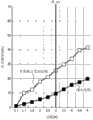
图3是用来对图1所示的结构和现有结构所带来的效果进行比较的图。FIG. 3 is a diagram for comparing the effects of the structure shown in FIG. 1 and the conventional structure.
-符号说明--Symbol Description-
20-开关动作部;30-第二整流电路;40-控制电路;50-增益切换电路;101-开关电源电路;102-第一整流电路;103-开关变压器;104-开关元件;105、106、111、114、119-电容器;108、109、112、115、116、117、120-电阻元件;107-光耦合器;110-并联稳压器;113-开关;118-二极管。20-switch action part; 30-second rectification circuit; 40-control circuit; 50-gain switching circuit; 101-switching power supply circuit; 102-first rectification circuit; 103-switching transformer; 104-switching element; 105, 106 , 111, 114, 119-capacitor; 108, 109, 112, 115, 116, 117, 120-resistive element; 107-optical coupler; 110-shunt regulator; 113-switch; 118-diode.
具体实施方式Detailed ways
下面,参照附图对本发明的一实施方式进行说明。Hereinafter, an embodiment of the present invention will be described with reference to the drawings.
图1是本发明的一实施方式所涉及的开关电源电路的结构图。开关电源电路101包括第一整流电路102、开关变压器103、开关动作部20、第二整流电路30以及控制电路40,该开关电源电路101由交流输入电AC生成直流输出电DC。还有,开关电源电路101构成为能够使该开关电源电路101的工作模式在待机模式和正常工作模式之间进行切换。FIG. 1 is a configuration diagram of a switching power supply circuit according to an embodiment of the present invention. The switching power supply circuit 101 includes a first rectification circuit 102 , a switching transformer 103 , a
第一整流电路102对例如商用电源输入即输入电AC进行整流,转换为直流电后输出。The first rectification circuit 102 rectifies, for example, commercial power input, that is, input power AC, converts it into direct current, and outputs it.
开关变压器103包括初级线圈103a和次级线圈103b。初级线圈103a连接在第一整流电路102和开关动作部20之间。次级线圈103b连接在第二整流电路30上。The switching transformer 103 includes a primary coil 103a and a secondary coil 103b. The primary coil 103 a is connected between the first rectifier circuit 102 and the
开关动作部20具有开关电源元件104、电容器105、106及电阻元件120。开关电源元件104通过使已由第一整流电路102整流的电流通断,从而将开关电流(switching current)供给初级线圈103a。并且,在次级线圈103b中感应产生了与开关电流相应的电。开关电源元件104根据反馈电压Vfb进行开关动作,该反馈电压Vfb与流向下文所述的光耦合器107的初级侧的电流相应地发生变化。The
第二整流电路30由二极管118和电容器119构成。在次级线圈103b中产生的电经二极管118和电容器119整流、平滑后成为直流电。已成为直流的电作为输出电DC被供给与声频系统的放大器等连接的负载。The
控制电路40通过从次级侧向初级侧反馈信号使得自第二整流电路30输出的电压成为规定电压,由此对开关动作部20进行反馈控制。控制电路40具有光耦合器107、并联稳压器110和增益切换电路50。The
光耦合器107由次级侧二极管和初级侧晶体管构成。在光耦合器107的次级侧和输出输出电DC的端子之间连接有电阻元件108、109。流向光耦合器107的电流和反馈电压Vfb根据被供给输出电DC的负载的大小而发生变化,由此开关电源元件104的开关频率发生变化。The photocoupler 107 is composed of a secondary side diode and a primary side transistor. Resistive elements 108 and 109 are connected between the secondary side of the photocoupler 107 and a terminal for outputting output power DC. The current flowing to the photocoupler 107 and the feedback voltage Vfb change according to the magnitude of the load to which the output power DC is supplied, whereby the switching frequency of the switching power supply element 104 changes.
并联稳压器110的阳极与光耦合器107的二极管连接,该并联稳压器110的阴极与接地连接。还有,由电阻元件116、117对第二整流电路30的输出电压进行分压而得到的电压被供给并联稳压器110的参考端子。The anode of the shunt regulator 110 is connected to the diode of the photocoupler 107, and the cathode of the shunt regulator 110 is connected to the ground. In addition, the voltage obtained by dividing the output voltage of the
增益切换电路50由电容器111、电阻元件112、开关113、电容器114及电阻元件115构成。根据来自外部的未图示出来的微型计算机等的控制信号对开关113进行开关控制。具体而言,当开关电源电路101处于正常工作模式时开关113断开,而当该开关电源电路101处于待机模式时开关113接通。当开关113断开时,电容器111和电阻元件112与并联稳压器110连接。另一方面,当开关113接通时,电容器111和电阻元件112以及电容器114和电阻元件115都与并联稳压器110连接。The
由此,在待机模式下流向光耦合器107的电流与第二整流电路30的输出电压的比率和在正常工作模式下的该比率得以切换。具体而言,若开关113断开,流向光耦合器107的电流与第二整流电路30的输出电压的比率就会下降。也就是说,并联稳压器110的增益提高,流向光耦合器107的电流减少。另一方面,若开关113接通,流向光耦合器107的电流与第二整流电路30的输出电压的比率就会提高。也就是说,并联稳压器110的增益降低,流向光耦合器107的电流增加。Thereby, the ratio of the current flowing to the photocoupler 107 to the output voltage of the
如上所述,切换并联稳压器110的增益使得在待机模式下的该增益和在正常工作模式下的该增益互不相同,从而流向光耦合器107的电流就会发生变化。并且,反馈电压Vfb就会与流向光耦合器107的电流相应地发生变化,从而开关电源元件104的开关频率得到反馈控制。As described above, switching the gain of the shunt regulator 110 makes the gain in the standby mode different from that in the normal operation mode, so that the current flowing to the optocoupler 107 changes. Then, the feedback voltage Vfb changes according to the current flowing to the photocoupler 107, and the switching frequency of the switching power supply element 104 is feedback-controlled.
接着,参照图1和图2对本实施方式所涉及的开关电源电路的工作情况进行说明。图2是表示本实施方式所涉及的开关电源电路的工作模式和开关频率之间的关系的图。此外,横轴表示时间,纵轴表示供给初级线圈103a的电压Vds。Next, the operation of the switching power supply circuit according to this embodiment will be described with reference to FIGS. 1 and 2 . FIG. 2 is a diagram showing the relationship between the operation mode and the switching frequency of the switching power supply circuit according to the present embodiment. In addition, the horizontal axis represents time, and the vertical axis represents the voltage Vds supplied to the primary coil 103a.
当开关电源电路101处于待机模式时,开关113接收到通知处于待机模式的控制信号后导通。由于开关113导通,因而并联稳压器110的增益下降,流向光耦合器107的电流增加。其结果是,由于开关电源元件104的反馈电压Vfb降低,因此以图2(a)所示的开关频率对开关电源元件104进行控制。When the switching power supply circuit 101 is in the standby mode, the switch 113 is turned on after receiving the control signal notifying that it is in the standby mode. Since the switch 113 is turned on, the gain of the shunt regulator 110 decreases and the current flowing to the optocoupler 107 increases. As a result, since the feedback voltage Vfb of the switching power supply element 104 decreases, the switching power supply element 104 is controlled at the switching frequency shown in FIG. 2( a ).
另一方面,当处于正常工作模式时,开关113由于接收到通知处于正常工作模式的信号,因而没有导通。由于开关113没有导通,因此并联稳压器110的增益上升,流向光耦合器107的电流减少。其结果是,由于反馈电压Vfb升高,因此以图2(b)所示的开关频率进行控制。On the other hand, when it is in the normal operation mode, the switch 113 is not turned on because it receives a signal notifying that it is in the normal operation mode. Since the switch 113 is not conducting, the gain of the shunt regulator 110 increases and the current flowing to the optocoupler 107 decreases. As a result, since the feedback voltage Vfb rises, control is performed at the switching frequency shown in FIG. 2( b ).
在此,待机模式时的开关频率被控制在声频范围(20Hz~20kHz)的下限值即20Hz以下。还有,正常工作模式时的开关频率被控制在声频范围的上限值即20kHz以上。Here, the switching frequency in the standby mode is controlled to be 20 Hz or less which is the lower limit of the audio frequency range (20 Hz to 20 kHz). In addition, the switching frequency in the normal working mode is controlled above 20 kHz, which is the upper limit of the audio frequency range.
在本实施方式中,为了实现上述开关频率,例如,用型号为STR2A155的IC(Integrated Circuit,集成电路)作为开关电源元件104,用型号为PC123X2YUP0F的IC作为光耦合器107,并且用型号为MM1431CURE的IC作为并联稳压器110。在这种情况下,例如只要将电容器111的电容值设为0.1μF,将电阻元件112的电阻值设为390kΩ,将电容器114的电容值设为0.1μF,并将电阻元件115的电阻值设为3.3kΩ即可。In this embodiment, in order to realize the above-mentioned switching frequency, for example, an IC (Integrated Circuit) with a model number of STR2A155 is used as the switching power supply element 104, an IC with a model number of PC123X2YUP0F is used as the optocoupler 107, and a model number is MM1431CURE IC as shunt regulator 110. In this case, for example, the capacitance value of the capacitor 111 is set to 0.1 μF, the resistance value of the resistance element 112 is set to 390 kΩ, the capacitance value of the capacitor 114 is set to 0.1 μF, and the resistance value of the resistance element 115 is set to It can be 3.3kΩ.
图3是用来对本实施方式所涉及的开关电源电路和现有开关电源电路所带来的效果进行比较的图。此外,横轴表示功耗,纵轴表示开关频率。还有,P__on表示开关电源电路接通电源时的状态,对应正常工作模式。FIG. 3 is a diagram for comparing the effects of the switching power supply circuit according to the present embodiment and a conventional switching power supply circuit. Also, the horizontal axis represents power consumption, and the vertical axis represents switching frequency. In addition, P__on represents the state when the switching power supply circuit is powered on, corresponding to the normal working mode.
在现有开关电源电路中,虽然在待机模式时功耗为0.05W,开关频率在20Hz以下,但是在接通电源时,也就是在开关电源电路从待机模式切换到正常工作模式时,功耗为3.2W,开关频率为10kHz。因此,由于在接通电源时开关频率包含在声频范围中,所以会产生噪声。In the existing switching power supply circuit, although the power consumption is 0.05W in standby mode and the switching frequency is below 20Hz, when the power is turned on, that is, when the switching power supply circuit switches from standby mode to normal operation mode, the power consumption It is 3.2W and the switching frequency is 10kHz. Therefore, since the switching frequency is included in the audio frequency range when the power is turned on, noise is generated.
与此相对,在本实施方式所涉及的开关电源电路101中,当处于待机模式时功耗为0.05W,开关频率在20Hz以下。并且,在接通电源时,功耗为3.2W,开关频率为25kHz。因此,开关电源电路101不论处于待机模式还是处于正常工作模式,开关频率都在声频范围之外,所以在待机模式时和在正常工作模式时开关变压器103都不会产生噪声。In contrast, in the switching power supply circuit 101 according to the present embodiment, the power consumption is 0.05 W in the standby mode, and the switching frequency is 20 Hz or less. And, when the power is turned on, the power consumption is 3.2W, and the switching frequency is 25kHz. Therefore, no matter whether the switching power supply circuit 101 is in the standby mode or in the normal working mode, the switching frequency is outside the audio frequency range, so the switching transformer 103 will not generate noise in the standby mode and in the normal working mode.
如上所述,根据本实施方式,因为在开关电源电路的待机模式和正常工作模式下都能够进行控制使开关频率在声频范围之外,所以不论处于哪种工作模式都能够抑制变压器的噪声。As described above, according to this embodiment, since the switching frequency can be controlled so that the switching frequency is out of the audio frequency range in both the standby mode and the normal operation mode of the switching power supply circuit, transformer noise can be suppressed regardless of the operation mode.
-产业实用性--Industrial Applicability-
本发明所涉及的开关电源电路能够谋求低功耗化,同时还能抑制当处于待机模式时和处于正常工作模式时变压器的噪声,所以对于要求在安静环境下使用的声频系统等的电源电路是很有用的。The switching power supply circuit involved in the present invention can achieve low power consumption, and can also suppress the noise of the transformer when it is in standby mode and in normal operation mode, so it is an excellent choice for power circuits such as audio systems that are required to be used in a quiet environment. very useful.
Claims (4)
Applications Claiming Priority (3)
| Application Number | Priority Date | Filing Date | Title |
|---|---|---|---|
| JP2012-002728 | 2012-01-11 | ||
| JP2012002728 | 2012-01-11 | ||
| PCT/JP2012/004453WO2013105150A1 (en) | 2012-01-11 | 2012-07-10 | Switching power supply circuit |
Publications (1)
| Publication Number | Publication Date |
|---|---|
| CN103299527Atrue CN103299527A (en) | 2013-09-11 |
Family
ID=48781129
Family Applications (1)
| Application Number | Title | Priority Date | Filing Date |
|---|---|---|---|
| CN2012800029545APendingCN103299527A (en) | 2012-01-11 | 2012-07-10 | Switching power supply circuit |
Country Status (5)
| Country | Link |
|---|---|
| US (1) | US8923020B2 (en) |
| EP (1) | EP2804303B1 (en) |
| JP (1) | JP6083668B2 (en) |
| CN (1) | CN103299527A (en) |
| WO (1) | WO2013105150A1 (en) |
Cited By (2)
| Publication number | Priority date | Publication date | Assignee | Title |
|---|---|---|---|---|
| CN105978301A (en)* | 2015-03-13 | 2016-09-28 | 恩智浦有限公司 | Control arrangement for a switched mode power supply |
| CN105978364A (en)* | 2015-12-31 | 2016-09-28 | 小米科技有限责任公司 | Power supply control system |
Families Citing this family (1)
| Publication number | Priority date | Publication date | Assignee | Title |
|---|---|---|---|---|
| CN108668402B (en)* | 2017-03-31 | 2021-06-08 | 朗德万斯公司 | Lamp driver for an LED lamp and LED lamp for arrangement in a fluorescent lamp fixture |
Citations (4)
| Publication number | Priority date | Publication date | Assignee | Title |
|---|---|---|---|---|
| JP2000184709A (en)* | 1998-12-11 | 2000-06-30 | Sanken Electric Co Ltd | Switching power supply equipment |
| CN1547797A (en)* | 2001-08-31 | 2004-11-17 | ���ṫ˾ | Switching power supply unit |
| JP2006050760A (en)* | 2004-08-04 | 2006-02-16 | New Japan Radio Co Ltd | Switching power supply circuit and control method therefor |
| CN101218737A (en)* | 2005-05-10 | 2008-07-09 | Nxp股份有限公司 | Feedback communication technique for switched mode power supply |
Family Cites Families (47)
| Publication number | Priority date | Publication date | Assignee | Title |
|---|---|---|---|---|
| JPH01133272A (en) | 1987-11-18 | 1989-05-25 | Mitsubishi Electric Corp | magnetic disk device |
| JPH0395238A (en) | 1989-09-07 | 1991-04-19 | Sumitomo Chem Co Ltd | foam |
| JP3095238B2 (en) | 1990-10-23 | 2000-10-03 | エア・ウォーター株式会社 | Ultra high purity nitrogen production equipment |
| JP3037050B2 (en)* | 1993-11-30 | 2000-04-24 | 三洋電機株式会社 | Power supply |
| JP3198944B2 (en)* | 1995-11-17 | 2001-08-13 | 株式会社村田製作所 | Switching power supply |
| KR0174724B1 (en)* | 1996-03-29 | 1999-04-01 | 김광호 | Display Monitor Power Supply with Power Factor Correction Circuit |
| US6104622A (en)* | 1997-04-30 | 2000-08-15 | Fidelix Y.K. | Power supply apparatus for reduction of power consumption |
| KR19990012879A (en)* | 1997-07-31 | 1999-02-25 | 이형도 | Power Factor Correction Circuit of Power Supply |
| JPH11235036A (en)* | 1998-02-09 | 1999-08-27 | Murata Mfg Co Ltd | Self-excited oscillation switching powder supply |
| JP2000116027A (en)* | 1998-03-10 | 2000-04-21 | Fiderikkusu:Kk | Power supply device |
| JP3614693B2 (en)* | 1999-01-13 | 2005-01-26 | 三菱電機株式会社 | Power control device |
| JP3386016B2 (en)* | 1999-01-18 | 2003-03-10 | 株式会社村田製作所 | Switching power supply |
| US6295217B1 (en)* | 1999-03-26 | 2001-09-25 | Sarnoff Corporation | Low power dissipation power supply and controller |
| KR100379057B1 (en)* | 1999-04-10 | 2003-04-08 | 페어차일드코리아반도체 주식회사 | A Burst Mode Switching Mode Power Supply |
| JP3475888B2 (en)* | 2000-01-11 | 2003-12-10 | 株式会社村田製作所 | Switching power supply |
| JP3409287B2 (en) | 2000-08-02 | 2003-05-26 | Smk株式会社 | Self-excited switching power supply circuit |
| JP2002084751A (en)* | 2000-09-01 | 2002-03-22 | Uinzu:Kk | Resonant power supply and power conversion method using the power supply |
| KR100376131B1 (en)* | 2000-09-22 | 2003-03-15 | 삼성전자주식회사 | Consumption power saving apparatus and controlling method in a stand-by mode |
| KR100438695B1 (en)* | 2001-03-09 | 2004-07-05 | 삼성전자주식회사 | Apparatus for controlling power supply and method thereof |
| US6510062B2 (en)* | 2001-06-25 | 2003-01-21 | Switch Power, Inc. | Method and circuit to bias output-side width modulation control in an isolating voltage converter system |
| KR100426696B1 (en)* | 2001-10-20 | 2004-04-14 | 삼성전자주식회사 | display device |
| JP3494223B2 (en)* | 2001-12-03 | 2004-02-09 | サンケン電気株式会社 | DC-DC converter |
| JP3496673B2 (en)* | 2002-01-11 | 2004-02-16 | サンケン電気株式会社 | DC power supply |
| US6952355B2 (en)* | 2002-07-22 | 2005-10-04 | Ops Power Llc | Two-stage converter using low permeability magnetics |
| KR100750906B1 (en)* | 2002-10-21 | 2007-08-22 | 페어차일드코리아반도체 주식회사 | Switched-Mode Power Supplies for Low Power Driving |
| JP3095238U (en)* | 2003-01-14 | 2003-07-25 | 船井電機株式会社 | Switching power supply circuit with standby mode function |
| US6839247B1 (en)* | 2003-07-10 | 2005-01-04 | System General Corp. | PFC-PWM controller having a power saving means |
| JP2007295761A (en)* | 2006-04-27 | 2007-11-08 | Matsushita Electric Ind Co Ltd | Switching power supply |
| TW200847602A (en)* | 2007-05-29 | 2008-12-01 | Richtek Techohnology Corp | Apparatus and method of improving flyback transformer light-loading efficacy |
| US8031496B2 (en)* | 2007-11-07 | 2011-10-04 | Panasonic Corporation | Driving circuit for power switching device, driving method thereof, and switching power supply apparatus |
| TWI390378B (en)* | 2008-05-14 | 2013-03-21 | Richtek Technology Corp | Control circuit and method of Chi - back power converter |
| JP2010022121A (en)* | 2008-07-10 | 2010-01-28 | Panasonic Corp | Switching power supply device and semiconductor device for switching power supply |
| US8654113B2 (en)* | 2008-09-19 | 2014-02-18 | Mstar Semiconductor, Inc. | Ultra-low-power display control circuit and associated method |
| JP5268615B2 (en)* | 2008-12-15 | 2013-08-21 | キヤノン株式会社 | Power supply device and image forming apparatus |
| WO2010083511A1 (en)* | 2009-01-19 | 2010-07-22 | Flextronics International Usa, Inc. | Controller for a power converter |
| JP2010206982A (en) | 2009-03-04 | 2010-09-16 | Nichicon Corp | Switching power supply device |
| JP2010220293A (en)* | 2009-03-13 | 2010-09-30 | Canon Inc | Switching power supply device |
| JP5341627B2 (en)* | 2009-06-11 | 2013-11-13 | パナソニック株式会社 | Semiconductor device and switching power supply device |
| CN102474186A (en)* | 2009-07-24 | 2012-05-23 | Nec显示器解决方案株式会社 | switching power supply and electronic device using the same |
| TWI387194B (en)* | 2009-08-14 | 2013-02-21 | Richpower Microelectronics | Apparatus and method for standby power saving of a flyback power converter |
| JP5731398B2 (en)* | 2009-11-25 | 2015-06-10 | ローム株式会社 | Control circuit for power adapter and DC / DC converter |
| JP5574846B2 (en)* | 2010-06-22 | 2014-08-20 | キヤノン株式会社 | Switching power supply |
| JP5587051B2 (en)* | 2010-06-22 | 2014-09-10 | キヤノン株式会社 | Switching power supply |
| JP5488274B2 (en)* | 2010-07-08 | 2014-05-14 | 富士電機株式会社 | Semiconductor integrated circuit and switching power supply device |
| JP5099183B2 (en)* | 2010-07-13 | 2012-12-12 | サンケン電気株式会社 | Start-up circuit |
| JP5683241B2 (en)* | 2010-12-06 | 2015-03-11 | キヤノン株式会社 | Switching power supply device and image forming apparatus |
| CN102291000B (en)* | 2011-08-29 | 2014-09-10 | 上海新进半导体制造有限公司 | Switch power supply integrated circuit |
- 2012
- 2012-07-10CNCN2012800029545Apatent/CN103299527A/enactivePending
- 2012-07-10WOPCT/JP2012/004453patent/WO2013105150A1/enactiveApplication Filing
- 2012-07-10USUS13/824,744patent/US8923020B2/enactiveActive
- 2012-07-10EPEP12840850.7Apatent/EP2804303B1/enactiveActive
- 2012-07-10JPJP2012555982Apatent/JP6083668B2/enactiveActive
Patent Citations (4)
| Publication number | Priority date | Publication date | Assignee | Title |
|---|---|---|---|---|
| JP2000184709A (en)* | 1998-12-11 | 2000-06-30 | Sanken Electric Co Ltd | Switching power supply equipment |
| CN1547797A (en)* | 2001-08-31 | 2004-11-17 | ���ṫ˾ | Switching power supply unit |
| JP2006050760A (en)* | 2004-08-04 | 2006-02-16 | New Japan Radio Co Ltd | Switching power supply circuit and control method therefor |
| CN101218737A (en)* | 2005-05-10 | 2008-07-09 | Nxp股份有限公司 | Feedback communication technique for switched mode power supply |
Cited By (4)
| Publication number | Priority date | Publication date | Assignee | Title |
|---|---|---|---|---|
| CN105978301A (en)* | 2015-03-13 | 2016-09-28 | 恩智浦有限公司 | Control arrangement for a switched mode power supply |
| CN105978301B (en)* | 2015-03-13 | 2019-12-27 | 恩智浦有限公司 | Control device for switching power supply |
| CN105978364A (en)* | 2015-12-31 | 2016-09-28 | 小米科技有限责任公司 | Power supply control system |
| CN105978364B (en)* | 2015-12-31 | 2018-11-30 | 小米科技有限责任公司 | Power control system |
Also Published As
| Publication number | Publication date |
|---|---|
| JP6083668B2 (en) | 2017-02-22 |
| EP2804303B1 (en) | 2018-11-28 |
| US8923020B2 (en) | 2014-12-30 |
| EP2804303A1 (en) | 2014-11-19 |
| WO2013105150A1 (en) | 2013-07-18 |
| EP2804303A4 (en) | 2015-07-01 |
| US20140185332A1 (en) | 2014-07-03 |
| JPWO2013105150A1 (en) | 2015-05-11 |
Similar Documents
| Publication | Publication Date | Title |
|---|---|---|
| US8194417B2 (en) | Two-stage switching power supply | |
| US10445281B2 (en) | Load detection apparatus and method for USB systems | |
| JP2013021861A (en) | Power-supply device and method of controlling the same | |
| TW201414155A (en) | Off-line power converter and integrated circuit suitable for use in same | |
| JP5746560B2 (en) | Switching power supply | |
| JPWO2014188711A1 (en) | DC power supply circuit | |
| JP2012196109A (en) | Control circuit of switching power supply device, and switching power supply device | |
| JP2006094696A (en) | Power factor correcting circuit and its output voltage control method | |
| JP2010166729A (en) | Switching power supply apparatus | |
| KR20060103499A (en) | Power supply | |
| CN202034910U (en) | Power supply with voltage limiting function | |
| KR100808246B1 (en) | Standby power supply | |
| CN103299527A (en) | Switching power supply circuit | |
| JP6268786B2 (en) | Power conditioner, power conditioner system, and control method of power conditioner | |
| CN105226933B (en) | Controller for removing audio noise of power converter and related method thereof | |
| JPWO2015114780A1 (en) | Capacitor input type smoothing circuit | |
| JP2013118780A (en) | Switching power supply device | |
| JP2012205365A (en) | Switching power supply device | |
| JP2012249466A (en) | Switching power supply device | |
| JP2011172346A (en) | Direct current power supply device, and voltage generation method | |
| JP2008079380A (en) | Power supply unit and power supply system | |
| KR20190019293A (en) | Switched-Mode Power Supply and operating method thereof | |
| CN205490129U (en) | Wide voltage starting system | |
| US20150155775A1 (en) | Ac-dc converter with adjustable output | |
| TWI568162B (en) | Power supply module, power supply device, and power controlling method |
Legal Events
| Date | Code | Title | Description |
|---|---|---|---|
| C06 | Publication | ||
| PB01 | Publication | ||
| C10 | Entry into substantive examination | ||
| SE01 | Entry into force of request for substantive examination | ||
| C02 | Deemed withdrawal of patent application after publication (patent law 2001) | ||
| WD01 | Invention patent application deemed withdrawn after publication | Application publication date:20130911 |