CN103298201A - Method and system for avoiding flicker for SSL devices - Google Patents
Method and system for avoiding flicker for SSL devicesDownload PDFInfo
- Publication number
- CN103298201A CN103298201ACN2013100602088ACN201310060208ACN103298201ACN 103298201 ACN103298201 ACN 103298201ACN 2013100602088 ACN2013100602088 ACN 2013100602088ACN 201310060208 ACN201310060208 ACN 201310060208ACN 103298201 ACN103298201 ACN 103298201A
- Authority
- CN
- China
- Prior art keywords
- voltage
- controller
- input voltage
- power converter
- ssl device
- Prior art date
- Legal status (The legal status is an assumption and is not a legal conclusion. Google has not performed a legal analysis and makes no representation as to the accuracy of the status listed.)
- Granted
Links
- 238000000034methodMethods0.000titleclaimsabstractdescription14
- 238000006243chemical reactionMethods0.000claimsabstractdescription37
- 239000007787solidSubstances0.000claimsdescription11
- 230000000737periodic effectEffects0.000claimsdescription7
- 230000008859changeEffects0.000abstractdescription6
- 230000008447perceptionEffects0.000abstract1
- 230000003287optical effectEffects0.000description15
- 238000004891communicationMethods0.000description12
- 238000001514detection methodMethods0.000description10
- 238000010586diagramMethods0.000description10
- 239000003990capacitorSubstances0.000description9
- 238000009499grossingMethods0.000description7
- 230000001965increasing effectEffects0.000description7
- 238000012545processingMethods0.000description6
- 230000001360synchronised effectEffects0.000description6
- 238000013500data storageMethods0.000description5
- 230000005611electricityEffects0.000description4
- 241000282412HomoSpecies0.000description1
- 230000008901benefitEffects0.000description1
- 239000002131composite materialSubstances0.000description1
- 230000000694effectsEffects0.000description1
- 238000004146energy storageMethods0.000description1
- 238000005516engineering processMethods0.000description1
- 230000005669field effectEffects0.000description1
- 230000007274generation of a signal involved in cell-cell signalingEffects0.000description1
- 230000017525heat dissipationEffects0.000description1
- 230000001939inductive effectEffects0.000description1
- 238000007726management methodMethods0.000description1
- 239000011159matrix materialSubstances0.000description1
- 229910044991metal oxideInorganic materials0.000description1
- 150000004706metal oxidesChemical class0.000description1
- 238000012986modificationMethods0.000description1
- 230000004048modificationEffects0.000description1
- 238000001208nuclear magnetic resonance pulse sequenceMethods0.000description1
- 230000009467reductionEffects0.000description1
- 230000004044responseEffects0.000description1
- 239000004065semiconductorSubstances0.000description1
- 230000035945sensitivityEffects0.000description1
- 230000003595spectral effectEffects0.000description1
- 230000000087stabilizing effectEffects0.000description1
- 230000003685thermal hair damageEffects0.000description1
- 238000012546transferMethods0.000description1
Images


Classifications
- H—ELECTRICITY
- H05—ELECTRIC TECHNIQUES NOT OTHERWISE PROVIDED FOR
- H05B—ELECTRIC HEATING; ELECTRIC LIGHT SOURCES NOT OTHERWISE PROVIDED FOR; CIRCUIT ARRANGEMENTS FOR ELECTRIC LIGHT SOURCES, IN GENERAL
- H05B47/00—Circuit arrangements for operating light sources in general, i.e. where the type of light source is not relevant
- H05B47/10—Controlling the light source
- H—ELECTRICITY
- H05—ELECTRIC TECHNIQUES NOT OTHERWISE PROVIDED FOR
- H05B—ELECTRIC HEATING; ELECTRIC LIGHT SOURCES NOT OTHERWISE PROVIDED FOR; CIRCUIT ARRANGEMENTS FOR ELECTRIC LIGHT SOURCES, IN GENERAL
- H05B45/00—Circuit arrangements for operating light-emitting diodes [LED]
- H05B45/10—Controlling the intensity of the light
- H—ELECTRICITY
- H05—ELECTRIC TECHNIQUES NOT OTHERWISE PROVIDED FOR
- H05B—ELECTRIC HEATING; ELECTRIC LIGHT SOURCES NOT OTHERWISE PROVIDED FOR; CIRCUIT ARRANGEMENTS FOR ELECTRIC LIGHT SOURCES, IN GENERAL
- H05B45/00—Circuit arrangements for operating light-emitting diodes [LED]
- H05B45/30—Driver circuits
- H05B45/32—Pulse-control circuits
- H—ELECTRICITY
- H05—ELECTRIC TECHNIQUES NOT OTHERWISE PROVIDED FOR
- H05B—ELECTRIC HEATING; ELECTRIC LIGHT SOURCES NOT OTHERWISE PROVIDED FOR; CIRCUIT ARRANGEMENTS FOR ELECTRIC LIGHT SOURCES, IN GENERAL
- H05B45/00—Circuit arrangements for operating light-emitting diodes [LED]
- H05B45/30—Driver circuits
- H05B45/37—Converter circuits
- H05B45/3725—Switched mode power supply [SMPS]
- H—ELECTRICITY
- H05—ELECTRIC TECHNIQUES NOT OTHERWISE PROVIDED FOR
- H05B—ELECTRIC HEATING; ELECTRIC LIGHT SOURCES NOT OTHERWISE PROVIDED FOR; CIRCUIT ARRANGEMENTS FOR ELECTRIC LIGHT SOURCES, IN GENERAL
- H05B45/00—Circuit arrangements for operating light-emitting diodes [LED]
- H05B45/50—Circuit arrangements for operating light-emitting diodes [LED] responsive to malfunctions or undesirable behaviour of LEDs; responsive to LED life; Protective circuits
- H05B45/59—Circuit arrangements for operating light-emitting diodes [LED] responsive to malfunctions or undesirable behaviour of LEDs; responsive to LED life; Protective circuits for reducing or suppressing flicker or glow effects
- Y—GENERAL TAGGING OF NEW TECHNOLOGICAL DEVELOPMENTS; GENERAL TAGGING OF CROSS-SECTIONAL TECHNOLOGIES SPANNING OVER SEVERAL SECTIONS OF THE IPC; TECHNICAL SUBJECTS COVERED BY FORMER USPC CROSS-REFERENCE ART COLLECTIONS [XRACs] AND DIGESTS
- Y02—TECHNOLOGIES OR APPLICATIONS FOR MITIGATION OR ADAPTATION AGAINST CLIMATE CHANGE
- Y02B—CLIMATE CHANGE MITIGATION TECHNOLOGIES RELATED TO BUILDINGS, e.g. HOUSING, HOUSE APPLIANCES OR RELATED END-USER APPLICATIONS
- Y02B20/00—Energy efficient lighting technologies, e.g. halogen lamps or gas discharge lamps
- Y02B20/30—Semiconductor lamps, e.g. solid state lamps [SSL] light emitting diodes [LED] or organic LED [OLED]
Landscapes
- Circuit Arrangement For Electric Light Sources In General (AREA)
- Dc-Dc Converters (AREA)
Abstract
Translated fromChinese
Description
Translated fromChinese技术领域technical field
本发明涉及照明系统,具体地,本发明涉及一种用于在固态照明(SSL)装置中避免闪烁的方法和系统,例如,LED(发光二极管)或OLED(有机LED)装置。The present invention relates to lighting systems, in particular the present invention relates to a method and system for avoiding flicker in solid state lighting (SSL) devices, eg LED (Light Emitting Diode) or OLED (Organic LED) devices.
背景技术Background technique
许多年来,GLS(通用照明)或白炽灯是居民照明用的第一选择。这些光源可以容易地耦合到市电供电电源,该市电供电电源可提供例如在电源频率为60Hz或50Hz下110V或230V的电压。新型光源例如LED(发光二极管)灯可提供非常小的负载(通常地,比等价GLS灯少一个数量级),然而,固态照明(SSL)装置例如LED或有机LED(OLED)装置需要复杂的驱动电路以向SSL装置提供(通常地,为一常数)负载电压以及向SSL装置提供一(通常地,为一常数)负载电流。For many years, GLS (General Lighting) or incandescent lamps were the first choice for residential lighting. These light sources can be easily coupled to a mains power supply which can provide a voltage of eg 110V or 230V at a mains frequency of 60Hz or 50Hz. New light sources such as LED (Light Emitting Diode) lamps can provide very small loads (typically, an order of magnitude less than equivalent GLS lamps), however, Solid State Lighting (SSL) devices such as LED or Organic LED (OLED) devices require complex driving The circuit provides a (generally, a constant) load voltage to the SSL device and a (generally, a constant) load current to the SSL device.
用于SSL装置的该驱动电路可用于将AC电源电压转换为可能的恒负载电压以及可能的恒负载电压。具体地,该驱动电路可用来控制负载电压和负载电流,这样,SSL装置不会发生人眼可看见的闪烁。这种可视的闪烁可以以100Hz(电源频率为50Hz的一交流电源电压)或120Hz(电源频率为60Hz下一交流电源电压)的频率出现。该闪烁可能是由于交流电源电压的正弦波原因导致的,在该正弦电源电压的每半个波形中,交流电源电压会降至SSL装置所需最小开启电压Von以下。因此,SSL装置会以100/120Hz的频率发生断开,从而使得光源(例如,SSL装置)发生恼人的闪烁效应,本发明致力于解决SSL装置的上述这些技术问题,描述了一种有效的方法和系统,以用于驱动SSL装置而不会发生可视的闪烁。This driver circuit for an SSL device can be used to convert the AC mains voltage to a possibly constant load voltage and possibly a constant load voltage. Specifically, the driving circuit can be used to control the load voltage and load current, so that the SSL device does not experience flicker visible to human eyes. This visible flicker can occur at a frequency of 100 Hz (for an AC mains voltage with a mains frequency of 50 Hz) or 120 Hz (for an AC mains voltage with a mains frequency of 60 Hz). This flicker may be due to the sinusoidal nature of the AC mains voltage, which drops below the minimum turn-on voltage Von required by the SSL device during each half waveform of the sinusoidal mains voltage. Therefore, the SSL device will be disconnected at a frequency of 100/120 Hz, resulting in an annoying flickering effect of the light source (for example, SSL device), the present invention aims to solve these above technical problems of the SSL device, and describes an effective method and systems for driving SSL devices without visible flicker.
发明内容Contents of the invention
在本发明的一方面,描述了一种用于固态照明(SSL)装置驱动电路的控制器。所述SSL装置可以为LED或OLED装置。所述控制器可以被制成一集成电路或一微控制器。所述驱动电路可包括一电源转换器,以将一变化输入电压转换为一用于SSL装置的驱动电压。例如,所述电源转换器可以为一升降压变换器或一谐振变换器。所述电源转换器可以以最大升压转换比被使用。换句话说,所述电源转换器可用于在变化输入电压和用于SSL装置的驱动电压(该电压通常为电源转换器的输出电压)之间至少提供一最大升压转换比。通常地,所述SSL装置的驱动电压对应于穿过所述SSL装置的电压(加上流过一电流源的电压降,所述电流源用于控制流经SSL装置的电流)。In one aspect of the invention, a controller for a solid state lighting (SSL) device driving circuit is described. The SSL device may be an LED or OLED device. The controller can be made as an integrated circuit or a microcontroller. The drive circuit may include a power converter to convert a varying input voltage to a drive voltage for the SSL device. For example, the power converter may be a buck-boost converter or a resonant converter. The power converter can be used with a maximum boost conversion ratio. In other words, the power converter is operable to provide at least a maximum boost conversion ratio between the varying input voltage and the driving voltage for the SSL device (which is typically the output voltage of the power converter). Typically, the drive voltage of the SSL device corresponds to the voltage across the SSL device (plus the voltage drop through a current source used to control the current flow through the SSL device).
所述变化输入电压可以来自一电源频率的AC电源电压。通常地,所述变化输入电压为一DC电压,所述DC电压为一使用整流器(例如,半波或全波整流器)的AC电源电压。这样,所述变化输入电压可包括多个周期,其中每个周期包括半个正弦周期。The varying input voltage may be derived from an AC mains voltage of a mains frequency. Typically, the varying input voltage is a DC voltage that is an AC mains voltage using a rectifier (eg, half-wave or full-wave rectifier). As such, the varying input voltage may comprise a plurality of periods, wherein each period comprises half a sinusoidal period.
所述控制器可以用于与所电源频率(该电源频率例如可以为50Hz或60Hz)同步。为了达到该目的,所述控制器可以用于检测所述变化输入电压(例如,使用一事件检测单元)以检测位于所述变化输入电压范围内的一预先确定的(周期的)电压值。进一步地,所述控制器可用于确定多个以一脉冲频率进行重复的脉冲间隔(所述多个脉冲间隔可以为脉冲间隔序列)。所述多个脉冲间隔可以被规则地间隔开。所述脉冲频率可以为所述周期频率的倍数,其中所述周期频率为所述变化输入电压的周期的频率(例如,所述周期频率可以为两倍电源频率)。所述脉冲频率可大于人眼可感知光强度变化的感知频率。所述感知频率的典型值位于400Hz的范围内。所述感知频率可以由以下事实来确定:人眼不能感知一些频率下的光密度变化,这些频率(对于给定的光密度水平)等于或大于所述感知频率。The controller may be used to synchronize with the frequency of the power supply (the power frequency may be, for example, 50 Hz or 60 Hz). To this end, the controller may be adapted to detect the varying input voltage (eg using an event detection unit) to detect a predetermined (periodic) voltage value within the varying input voltage range. Further, the controller may be used to determine a plurality of pulse intervals repeated at a pulse frequency (the plurality of pulse intervals may be a sequence of pulse intervals). The plurality of pulse intervals may be regularly spaced. The pulse frequency may be a multiple of the cycle frequency, where the cycle frequency is the frequency of the cycle of the varying input voltage (eg, the cycle frequency may be twice the supply frequency). The pulse frequency may be greater than the perceptual frequency at which changes in light intensity can be perceived by human eyes. Typical values for the perceived frequency lie in the range of 400 Hz. The perceived frequency may be determined by the fact that the human eye cannot perceive changes in optical density at frequencies that (for a given optical density level) are equal to or greater than the perceived frequency.
如前所示,所述控制器可用于确定多个被规则间隔开的脉冲间隔。在所述变化输入电压的周期和/或跨过随后所述变化输入电压下一周期边界的范围内,所述多个脉冲间隔可以被规则地间隔开。在一实施例中,所述控制器可用于确定跨越多个所述变化输入电压周期的多个脉冲间隔,其中,所述多个脉冲间隔中的每个间隔被定位在其直接相邻的、在前的和/或在后的一脉冲间隔的恒定时间距离处。换句话说,所述控制器可用来确定多个脉冲间隔(或脉冲间隔序列),这样,所述脉冲间隔序列仅包括具有多个频率(该多个频率等于或大于所述脉冲频率)的频率分量。As previously indicated, the controller can be used to determine a plurality of regularly spaced pulse intervals. The plurality of pulse intervals may be regularly spaced over a period of the varying input voltage and/or across a boundary of a subsequent period of the varying input voltage. In an embodiment, the controller is operable to determine a plurality of pulse intervals spanning a plurality of periods of the varying input voltage, wherein each interval of the plurality of pulse intervals is positioned in its immediate adjacent, At a constant time distance preceding and/or following a pulse interval. In other words, the controller can be configured to determine a plurality of pulse intervals (or a sequence of pulse intervals) such that the sequence of pulse intervals includes only frequencies having a frequency equal to or greater than the pulse frequency portion.
所述控制器可用于定位所述多个脉冲间隔,这样,位于所述多个脉冲间隔范围内的所述变化输入电压可大于或等于一预设最小输入电压。所述预设最小输入电压可以根据所述SSL装置的开电压除以所述最大升压转换比来确定。作为示例地,所述预设最小输入电压可以通过使用所述SSL装置的开电压除以所述最大升压转换比来确定。如果所述SSL装置与一电流源串联,所述预设最小输入电压可以根据所述SSL装置的开电压、流经所述电流源的最小电压降以及所述最大升压转换比来确定。作为示例地,所述预设最小输入电压可以通过将所述SSL装置的开电压与流经所述电流源的最小电压降的和除以所述最大升转换压比来确定。The controller can be configured to position the plurality of pulse intervals such that the varying input voltage within the range of the plurality of pulse intervals is greater than or equal to a predetermined minimum input voltage. The preset minimum input voltage may be determined according to dividing the on-voltage of the SSL device by the maximum boost conversion ratio. As an example, the preset minimum input voltage may be determined by dividing the turn-on voltage of the SSL device by the maximum boost conversion ratio. If the SSL device is connected in series with a current source, the preset minimum input voltage may be determined according to the turn-on voltage of the SSL device, the minimum voltage drop across the current source, and the maximum boost conversion ratio. As an example, the preset minimum input voltage may be determined by dividing the sum of the on-voltage of the SSL device and the minimum voltage drop through the current source by the maximum up-conversion voltage ratio.
所述控制器可用于控制所述电源转换器,以产生用于所述SSL装置的驱动电压。这样,位于所述多个脉冲间隔范围内的所述驱动电压至少与所述SSL装置的开电压(以及流经所述电流源的可能最小电压降)对应。进一步地,所述控制器可用于控制电源转换器,以在所述多个脉冲间隔之外的时间点(即,两个脉冲间隔之间)不产生驱动电压。可选地,所述控制器可用来控制所述电源转换器,以使得在所述多个脉冲间隔之外的时间点所述SSL装置不会发射可见光(但可以发射不可见频率范围内的光)。The controller is operable to control the power converter to generate a driving voltage for the SSL device. Thus, the drive voltage within the plurality of pulse intervals corresponds at least to the ON voltage of the SSL device (and the possible smallest voltage drop across the current source). Further, the controller may be used to control the power converter so as not to generate the driving voltage at time points other than the plurality of pulse intervals (ie, between two pulse intervals). Optionally, the controller is operable to control the power converter such that at time points outside of the plurality of pulse intervals the SSL device does not emit visible light (but emits light in an invisible frequency range ).
如前所示,所述SSL装置可以与一向所述SSL装置提供驱动电流的电流源进行串联。所述控制器可用来控制与所述SSL装置串联的所述电流源,以提供一位于所述多个脉冲间隔范围内的驱动电流,从而控制所述SSL装置发出与所述驱动电流对应光密度水平的光。通常地,一恒定驱动电流可以用来向所述SSL装置发射的光提供一恒定密度水平。所述控制器可用于控制所述电流源,以提供所述多个脉冲间隔范围内的过载驱动电流,以使得所述SSL装置在所述多个脉冲间隔范围内的过载模式下进行运行。所述过载驱动电流超过一最大驱动电流,需要对所述SSL装置进行配制以使其能够抵制住该最大驱动电流。换句话说,所述SSL装置可以在所述多个脉冲间隔范围内递增光密度水平下运行以发光,从而补偿所述多个脉冲间隔之间时间点SSL装置没有发出可见光的情况。As previously indicated, the SSL device may be connected in series with a current source that provides drive current to the SSL device. The controller may be used to control the current source connected in series with the SSL device to provide a driving current within the range of the plurality of pulse intervals, thereby controlling the SSL device to emit an optical density corresponding to the driving current horizontal light. Generally, a constant drive current can be used to provide a constant density level to the light emitted by the SSL device. The controller may be used to control the current source to provide an overload driving current within the range of the plurality of pulse intervals, so that the SSL device operates in an overload mode within the range of the plurality of pulse intervals. The overload drive current exceeds a maximum drive current, and the SSL device needs to be configured to withstand the maximum drive current. In other words, the SSL device may operate to emit light at increasing optical density levels over the plurality of pulse intervals, thereby compensating for the absence of visible light from the SSL device at times between the plurality of pulse intervals.
通常地,所述电源转换器可用于在所述变化输入电压和用于SSL装置的所述驱动电压之间提供多个电压转换比。进一步地,通常地,所述驱动电压(即:所述电源转换器的输出电压)包括有所述SSL装置的开电压以及流经所述电流源(所述电流源与所述SSL装置串联)的电压降。所述控制器可用来检测所述变化输入电压以及在检测到的所述输入电压的基础上控制所述电源转换器。具体地,所述控制器可用来控制所述电源转换器,以使得流经所电流源的电压降被保持在一流经所述电流源的预设最大电压降之下。这样,可以保证SSL装置驱动电路产生的功率损耗得到减少。所述控制器还可用来控制所述电源转换器,以使得流经所电流源的电压降被保持为或在一流经所述电流源的预设最大电压降之下(可能需要对电流源进行操作)。Generally, the power converter is operable to provide multiple voltage conversion ratios between the varying input voltage and the drive voltage for the SSL device. Further, generally, the driving voltage (namely: the output voltage of the power converter) includes the open voltage of the SSL device and flows through the current source (the current source is connected in series with the SSL device) voltage drop. The controller is operable to detect the varying input voltage and control the power converter based on the detected input voltage. Specifically, the controller is operable to control the power converter such that the voltage drop across the current source is kept below a preset maximum voltage drop across the current source. In this way, it can be ensured that the power loss generated by the driving circuit of the SSL device is reduced. The controller can also be used to control the power converter so that the voltage drop across the current source is maintained at or below a preset maximum voltage drop across the current source (possibly requiring the current source to operate).
如上所示,通常地,所述变化输入电压包括周期性的输入电压周期,所述输入电压周期以两倍所述电源频率作为周期频率。通常地,所述多个脉冲间隔位于多个输入电压周期范围内,即:所述脉冲间隔序列跨过邻近输入电压周期的一个或多个周期边界。所述多个输入电压周期中的每一个可以包括所述多个脉冲间隔一个各自的子集。换句话说,通常地,所述多个输入电压周期中的每一个包括所述多个脉冲间隔中的一个或多个间隔,例如,所述多个输入电压周期中的每一个包括所述多个脉冲间隔中的相同数目个脉冲间隔。通常地,每个输入电压周期中的脉冲间隔数目由所述脉冲频率和所述周期频率的比率确定。包括在所述子集中的所述脉冲间隔可以被定位在各个输入电压周期的所述各个输入电压周期的相应时间间隔处。换句话说,包括在所述输入电压周期中的所述脉冲间隔可以被定位在所述输入电压周期的相应位置处。As indicated above, generally, the varying input voltage includes a periodic input voltage cycle with twice the frequency of the power supply as the cycle frequency. Typically, the plurality of pulse intervals are within a range of a plurality of input voltage cycles, that is, the sequence of pulse intervals crosses one or more cycle boundaries adjacent to the input voltage cycle. Each of the plurality of input voltage cycles may include a respective subset of the plurality of pulse intervals. In other words, typically, each of the plurality of input voltage cycles includes one or more intervals of the plurality of pulse intervals, for example, each of the plurality of input voltage cycles includes the plurality of The same number of pulse intervals in the pulse interval. Typically, the number of pulse intervals per input voltage cycle is determined by the ratio of the pulse frequency to the cycle frequency. The pulse intervals included in the subset may be positioned at respective time intervals of the respective input voltage cycles. In other words, the pulse intervals included in the input voltage cycle may be positioned at corresponding positions of the input voltage cycle.
所述控制器可用于检测来自所述多个输入电压周期中第一输入电压周期期间的所述驱动电压,以及用于在所述第一电压周期期间检测的驱动电压的基础上控制所述第一电压周期随后的第二输入电压周期期间的所述电源转换器。具体地,所述控制器可用于检测所述第一输入电压周期的脉冲间隔内的所述驱动电压,以及用于在所述第一输入电压周期的脉冲间隔内检测的所述驱动电压的基础上控制所述第二输入电压周期的对应脉冲间隔内的所述电源转换器。可选地或附加地,所述控制器可用来存储控制参数,所述控制参数用于控制一第一输入电压周期的一脉冲间隔内的电源转换器,以及用于使用所述存储的控制参数(例如,用于所述电源转换器的参数)控制一第二输入电压周期的一对应脉冲间隔内的电源转换器。这样,所述控制器可用于在一个或多个在先输入电压周期内执行的所述电源转换器控制的基础上,在一电流输入电压周期内调整所述电源转换器的控制。The controller is operable to detect the driving voltage from during a first input voltage period of the plurality of input voltage periods, and to control the first driving voltage based on the detected driving voltage during the first voltage period. the power converter during a second input voltage cycle following a voltage cycle. Specifically, the controller may be used to detect the driving voltage within the pulse interval of the first input voltage cycle, and the basis for the driving voltage detected within the pulse interval of the first input voltage cycle controlling the power converter during corresponding pulse intervals of the second input voltage cycle. Alternatively or additionally, the controller may be operable to store control parameters for controlling the power converter within a pulse interval of a first input voltage cycle, and for using the stored control parameters (eg, parameters for the power converter) control the power converter within a corresponding pulse interval of a second input voltage cycle. In this way, the controller is operable to adjust the control of the power converter during a current input voltage cycle based on the control of the power converter performed during one or more preceding input voltage cycles.
所述控制器可用于接收关于SSL装置在所述多个脉冲间隔间时间点的环境光密度的信息,以及用于在所述接收到的信息的基础上控制所述电源转换器。这样,所述SSL装置的脉冲运行可用于自动调整所述SSL装置相对于环境光条件的光密度。The controller is operable to receive information about an ambient light density of the SSL device at points in time between the plurality of pulse intervals, and to control the power converter based on the received information. In this way, pulsed operation of the SSL device can be used to automatically adjust the optical density of the SSL device relative to ambient light conditions.
在本发明的另一方面,描述了一种适用于固态照明(SSL)装置的驱动电路。所述驱动电路可以被制成一集成电路。所述驱动电路包括一电源转换器,所述电源转换器用于将一变化输入电压转换为一用于所述SSL装置的驱动电压。所述输入电压由具有电源频率的一整流后AC电源电压提供。进一步地,所述驱动电路包括一本发明描述的各方面的控制器,以用于控制所述电源转换器,从而生成用于所述SSL装置的、位于多个脉冲间隔范围内的驱动电压。In another aspect of the invention, a driver circuit suitable for a solid state lighting (SSL) device is described. The drive circuit can be made as an integrated circuit. The drive circuit includes a power converter for converting a varying input voltage to a drive voltage for the SSL device. The input voltage is provided by a rectified AC mains voltage having a mains frequency. Further, the drive circuit includes a controller according to the aspects described in the present invention, for controlling the power converter, so as to generate a drive voltage for the SSL device within a range of a plurality of pulse intervals.
在本发明的另一方面,描述了一灯泡装置。所述灯泡装置包括一电连接模块,以用于电连接到一供电电源,以提供一输入电压波形。进一步地,所述灯泡装置包括一本发明描述的各方面的驱动电路,以用于将所述输入电压波形转换为用于固态照明(SSL)装置的驱动信号。另外,所述灯泡装置包括所述SSL装置,所述SSL装置根据所述驱动信号提供光源。In another aspect of the invention, a light bulb assembly is described. The light bulb device includes an electrical connection module for electrically connecting to a power supply to provide an input voltage waveform. Further, the light bulb device includes a driving circuit according to the aspects described in the present invention, for converting the input voltage waveform into a driving signal for a solid state lighting (SSL) device. In addition, the light bulb device includes the SSL device that provides a light source according to the drive signal.
在本发明的另一方面,描述了一种用于控制固态照明(SSL)装置的驱动电路的方法。其中,所述驱动电路包括一电源转换器,所述电源转换器用于将一变化输入电压转换为一用于所述SSL装置的驱动电压。所述输入电压由具有电源频率的一AC电源电压提供。以最大升压转换比对所述电源转换器进行使用。所述方法包括:同步为所述电源频率;确定一脉冲频率下的多个脉冲间隔。可以对所述脉冲频率进行选择,以使之大于人眼可感知光密度变化的可感知频率。位于所述多个脉冲间隔范围内的所述变化输入电压可大于或等于一预设最小输入电压,所述最小输入电压可对应于除以所述最大升压转换比的所述SSL装置的一开电压。所述方法进一步可包括:控制所述电源转换器,以生成用于所述SSL装置的驱动电压,所述驱动电压位于所述多个脉冲间隔范围内,这样,位于所述多个脉冲间隔内所述驱动电压至少对应于所述SSL装置的开电压。In another aspect of the invention, a method for controlling a driving circuit of a solid state lighting (SSL) device is described. Wherein, the driving circuit includes a power converter for converting a varying input voltage into a driving voltage for the SSL device. The input voltage is provided by an AC mains voltage having a mains frequency. The power converter is used with a maximum boost conversion ratio. The method includes: synchronizing to the power supply frequency; and determining a plurality of pulse intervals at a pulse frequency. The pulse frequency may be chosen to be greater than the perceivable frequency at which changes in optical density are perceivable by the human eye. The varying input voltage within the plurality of pulse intervals may be greater than or equal to a predetermined minimum input voltage, which may correspond to a voltage of the SSL device divided by the maximum boost conversion ratio. open voltage. The method may further include controlling the power converter to generate a drive voltage for the SSL device, the drive voltage being within the range of the plurality of pulse intervals such that within the plurality of pulse intervals The drive voltage corresponds at least to an on voltage of the SSL device.
附图说明Description of drawings
下面将参考附图,以示例的形式对本发明进行详细描述,其中:The present invention will be described in detail below in the form of examples with reference to the accompanying drawings, wherein:
图1为示例性灯泡装置的框图;Figure 1 is a block diagram of an exemplary light bulb device;
图2a为用于SSL装置的一驱动电路的一示例性组成部分的框图;Figure 2a is a block diagram of an exemplary component of a driver circuit for an SSL device;
图2b为一驱动电路的控制器组成部分的框图;Figure 2b is a block diagram of the controller components of a drive circuit;
图2c为用于SSL装置的一驱动电路的一示例性组成部分的框图;Figure 2c is a block diagram of an exemplary component of a driver circuit for an SSL device;
图3为用于SSL装置的一示例性驱动电路的电路框图;以及FIG. 3 is a block circuit diagram of an exemplary driving circuit for an SSL device; and
图4为一驱动电源电压和一驱动电压的示意图。FIG. 4 is a schematic diagram of a driving power supply voltage and a driving voltage.
具体实施方式Detailed ways
在本发明中,灯泡“装置”包括所有用于代替传统基于白炽灯丝灯泡的组件,特别是用于连接到标准供电电源的灯泡。在英式英语(以及本发明申请文件)中,该供电电源指的是“电源”电力,而在美式英语中,该电源指的是电源线路,该电源的其它术语包括AC电源、线路功率、家用电力以及电网电力。应注意,这些术语是可以互换的,具有相同的意义。In the present invention, a light bulb "set" includes all components intended to replace conventional incandescent filament-based light bulbs, in particular those intended to be connected to a standard mains supply. In British English (and in this patent application) the power supply refers to "mains" electricity, while in American English the power supply refers to the power line. Other terms for the power supply include AC power, line power, Household electricity and grid electricity. It should be noted that these terms are interchangeable and have the same meaning.
通常地,欧洲电力为230-240VAC、电源频率为50Hz,在北美为110-120VAC、60Hz。本发明中的原理可移植到任何合适的电力电源上,包括所述的电力/电源线路,以及整流后的AC供电电源。Generally, the electricity in Europe is 230-240VAC and the power frequency is 50Hz, and in North America it is 110-120VAC and 60Hz. The principles of the present invention can be transferred to any suitable power source, including the described power/power line, and rectified AC power supply.
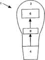
图1为一灯泡装置的示意图。所述装置1包括一灯泡外壳2以及一电连接模块4,所述电连接模块4可以为螺旋式或卡口式、或任何其它合适的可连接到灯泡插座的类型。电连接模块4的典型示例有欧洲的E11、E14以及E27螺旋式电连接模块以及北美的E12、E17以及E26螺旋式电连接模块。进一步地,光源6(也可以称作SSL装置)设置在外壳2中。用作该光源6的示例有固态照明光源6,例如,发光二极管(LED)或有机发光二极管(OLED)。光源6可以通过单一光发射装置来提供,或通过多个LED来提供。典型的SSL装置6包括串联设置的多个LED,这样,SSL装置的开电压Von为单个LED开电压的总和。SSL装置开电压的典型值位于100V–150V的范围内。FIG. 1 is a schematic diagram of a light bulb device. The device 1 comprises a
一般情况下,不论SSL装置6发射光的密度大小,流经SSL装置6的电压降几乎保持为一恒量(为SSL装置6的开电压Von)。通常地,SSL装置6发射光的密度大小可由流经SSL装置6的驱动电流来控制。Generally, regardless of the intensity of light emitted by the
驱动电路8位于灯泡外壳2中,用于将通过电连接模块4接收的电源电力(即:市电电源)转换为控制的驱动电压和驱动电流,以用于光源6。当光源6为固态光源时,驱动电路8用于向光源6提供控制的直流驱动电流。The driving
外壳2为光源和驱动组件提供了一合适的坚固的空间,包括有光学元件,以从灯泡装置提供期望的光输出。由于光源温度管理在最大光输出和光源寿命上具有重要地位,因此,外壳2还可以提供散热的功能。因此,通常地,外壳被设计成能够将光源产生的热量传导出光源以及传导出整个装置的设计。The
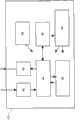
图2a示出了SSL装置250的驱动电路200的示例性组成部分。该驱动电路200包括一整流器210,整流器210可接收来自所述市电电源的交流(AC)电源电力,并在其输出端输出一整流后电流(DC)。该DC电源被电源转换器230接收,电源转换器230用于输出一控制的DC驱动电压至SSL装置250。进一步地,驱动电路200包括一电流源240,电流源240用于提供一可控的驱动电流至SSL装置250。驱动信号(包括驱动电压和驱动电流)的电压和电流特征由光源6(即SSL装置250中)使用的LED灯的数量和类型确定。而向SSL装置250提供的电源可以根据SSL装置250的期望运行条件进行控制。在一实施例中,SSL装置250包括串联的多个LED灯,此时则需要具有驱动电压为50V甚至更高的驱动信号。一般情况下,驱动电压可以位于10V到超过100V的范围,这决定于包括在SSL装置250中的LED的数量。FIG. 2 a shows exemplary components of a
驱动电路200可以进一步包括一控制器220,该控制器220可用于控制电源转换器230以及电流源240,以产生合适的、具有整流后电源电压功能的驱动信号(即:合适的驱动电压和合适的驱动电流)。具体地,控制器220可用于在整流器210整流后(但是变化的)电压的基础上调整电源转换器230的电压转换比。进一步地,控制器220可用于控制电流源240,以向SSL装置250提供一合适的驱动电流,从而控制由SSL装置250发射所述密度的光。The driving
电源转换器230可以包括一电感储能装置以及一开关装置。开关装置可由控制器220进行控制。该开关装置可以为一金属氧化物半导体场效应晶体管(MOSFET)装置或其它适用于开关高电压(例如,十几个伏特)的装置。尽管如此,应注意,控制器220可包括开关装置本身,以直接控制适合驱动电压的提供。电源转换器230可以由任何合适的电路提供。例如,降压变换器电路、升压变换器电路、降/升压变换器电路、SEPIC(单端初级电感变换器)电路或回扫电路,以用于电源转换器230。尽管如此,应注意,电源转换器230并不限定为开关模式的电源转换器,也可以是基于线性调节器或使用开关电容或结合这些转换器技术的其它转换器。The
图2b示出了控制器220的框图。控制器220包括一被连接用于接收传感器/反馈信号S的事件检测单元42(例如,用于接收整流器210提供的整流电压)、一用于(例如,向电源转换器230和/或电流源240)输出控制信号C的输出控制器43、一用于对系统进行全局控制的处理单元44以及一用于存储数据的数据存储单元46,所述数据用于供处理装置/单元使用。通信输入/输出单元48用来使得处理单元44可与其它装置进行通信,例如,使用合适的有线或无线通信协议与其它装置进行通信。控制器220还包括一供电电源调节器50以及一用于向处理单元44提供参考时间信号的时钟信号生成器52。供电电源调节器50可向控制器220内的装置提供电源。时钟信号生成器52可用于根据传感器/反馈信号S(例如,来自整流器210提供的整流电压信号)生成一时钟信号,以使得驱动电路200与电源频率同步。换句话说,为了使驱动电路200与电源周期同步,时钟信号生成器52可以利用电源周期的周期。FIG. 2 b shows a block diagram of the
处理单元44的运行可生成控制信号C,以控制电源转换器230和/或电流源240中的开关装置。通常地,控制信号可以为脉宽调制(PWM)信号,以控制电源转换器240中开关装置的占空比(即:开关“开状态”的时间与一完整通信周期长度的比值,所述完整通信周期包括开状态阶段以及随后的关状态阶段),从而控制输出的驱动电压。在一实施例中,控制器220可作制成一微控制器或一集成电路。Operation of the processing unit 44 may generate control signals C to control switching devices in the
图3示出了驱动电路8、300的一电路框图,该驱动电路包括一单级LED电源转换器230。电路框图300示出了一AC电源301以及与EMI(电磁干扰)过滤器元件303、304结合的过滤器302。驱动电路300包括一控制器310(例如,图2a和图2b中的控制器220),控制器310连接在一稳定电容311上。控制器310包括一启动和检测引脚305。在本实施例中,引脚305用于检测整流后的输入电压波形,以使得控制器310与电源周期同步,从而控制驱动电路300生成适合的驱动电压和驱动电流。在本实施例中,控制器310包括图2b中描述的控制器220的一些或所有组件。FIG. 3 shows a block diagram of a
进一步地,控制器310包括一内部电源开关,该开关连接在引脚313上,从而与外部电子元件307、308、309以及312结合实现一开关电源转换器230。在本实施例中,LED电源转换器230可制成一降压变换器315。可以对位于控制器310中的所述电源开关的占空比进行调整以控制驱动电压,使其具有整流后电源电压波形的功能。进一步地,位于控制器310中的所述电源开关的占空比进行调整,以调整驱动电路300适应LED装置320的LED灯参数(例如,串联的LED数量)。在本实施例中,控制器还可以包括电流源240,以用于控制流经SSL装置320驱动电流。Further, the
图4示出了电源电压周期的电压/时间关系图400。可以看出,AC电源电压401以周期率50Hz的正弦方式进行振荡。进一步,图400示出了整流器302、210输出端的整流后电压402。作为示例地,假设SSL装置250、320需要150V的开电压Von。这样,为了保证SSL装置250、320发光,由电源转换器230、315提供的驱动电压应等于或高于150V的开电压Von。进一步地,为了减少驱动电路300、200的损耗,流经电流源240的电压降应减少到最小(被减少)。通常地,由电源转换器230提供的输出电压(即:驱动电压)为流经SSL装置250开电压Von和流经电流源240的电压降(如果输出电压大于SSL装置250的开电压Von)的总和。进一步地,为了便于说明,但不用于限制本实施例,在这里可假设电源转换器230为一复合的升压/降压转换器(例如,升压/降压变换器),可提供值为3的最大升压转换比(即:电源转换器230的输出电压可高达输入电压的3倍)以及值为2最大降压转换比(即:电源转换器230的输出电压比其输入电压低2倍)。FIG. 4 shows a voltage/time graph 400 of a supply voltage cycle. It can be seen that the AC supply voltage 401 oscillates in a sinusoidal manner with a period rate of 50 Hz. Further, the graph 400 shows the rectified voltage 402 at the output of the
在上述假设前提下,可以看出,在AC电源电压401的过零点401附近区域中,整流后电压402下降到50V以下,这样,(可提供最大升压转换比为3的)电源转换器230无法提供SSL装置250所必需的开电压Von。结果,只要存在AC电源电压401的过零点401,SSL装置250就不会发光。可以看出,过零点404出现的频率为两倍电源频率,即在本实施例中频率为100Hz。由于后者频率(即两倍电源频率)指的是整流后电源电压相同(半波)周期的出现频率,因此,后者频率(即两倍电源频率)可以被称为周期频率。所以由SSL装置250生成的光会以频率为100Hz被阻断,从而产生100Hz的可视闪烁。Under the above assumptions, it can be seen that in the area around the zero-crossing point 401 of the AC power supply voltage 401, the rectified voltage 402 drops below 50V, so that the power converter 230 (with a maximum boost conversion ratio of 3) The ON voltage Von required by the
一种克服100Hz闪烁问题的方法是在整流器210的输出端利用一较大的平滑电容。该较大的平滑电容用于对整流后的电压波形402进行平滑操作,以移除整流后电压波形402的电压骤降点404。尽管如此,优选地,可将平滑电容(以及,具体地,较大尺寸的平滑电容)与驱动电路200、300整合到一起(同样,也可以将平滑电容外部连接到包括驱动电路200、300的集成电路上)。进一步地,由于该平滑电容的使用寿命相对较短,因此,会减少驱动电路200、300以及整个灯泡装置1的使用寿命。One way to overcome the 100 Hz flicker problem is to use a large smoothing capacitor at the output of the rectifier 210 . The larger smoothing capacitor is used to smooth the rectified voltage waveform 402 to remove the voltage dip point 404 of the rectified voltage waveform 402 . However, preferably, smoothing capacitors (and, in particular, larger-sized smoothing capacitors) can be integrated with the
在本发明中,通过将闪烁频率移至人眼无法不可见的频率范围来解决100Hz的闪烁问题。可以知道,人眼对光密度变化的敏感性决定于频率。作为示例地,人眼可以观察到频率为100Hz以及以下的光密度变化。当处于闪烁光线条件下时,人难以准确地估计距离。由于这种原因,闪烁光源(例如,闪烁频率为100Hz的光源)被禁止使用在许多应用中,例如,交通应用(例如,隧道中)。另一方面,可以知道当光密度变化频率等于或高某一频率(例如,400Hz)时,人眼无法觉察闪烁光以及感知一平均光密度的闪烁光。这样,人眼可以被模拟为一作为光变化的低通过滤器,其中,低通过滤器可以为一截止频率大约为400Hz的低通过滤器。In the present invention, the 100 Hz flickering problem is solved by moving the flickering frequency to a frequency range that cannot be invisible to human eyes. It can be known that the sensitivity of the human eye to changes in optical density depends on the frequency. As an example, human eyes can observe changes in optical density at a frequency of 100 Hz and below. Humans have difficulty estimating distances accurately when exposed to flickering light conditions. For this reason, flickering light sources (eg, light sources with a flickering frequency of 100 Hz) are prohibited in many applications, eg, traffic applications (eg, in tunnels). On the other hand, it can be known that when the optical density variation frequency is equal to or higher than a certain frequency (for example, 400 Hz), human eyes cannot perceive the flickering light and perceive the flickering light of an average optical density. In this way, the human eye can be simulated as a low-pass filter that changes as light, wherein the low-pass filter can be a low-pass filter with a cutoff frequency of about 400 Hz.
本发明利用了上述原理,以等于或高于用于人眼密度变化的截止频率(例如等于或高于400Hz)在脉冲模式下驱动SSL装置250,如图4所示。在图4中示出了脉冲间隔403序列,为了向SSL装置250生成驱动电压以及驱动电流,在这些间隔中电源转换器230和/或电流源240被激活。示出的脉冲间隔403的频率例如可以为500Hz(即:高于人眼密度变化截止频率的一个频率)。优选地,该脉冲频率为周期频率的倍数。进一步地,脉冲间隔403与电源周期同步,这样,对于每个脉冲间隔403,整流后电压402等于或高于一预设的电压阀值VT(例如,在本实施例中VT=50V)。通常地,预设的电压阀值VT决定于电源转换器230(特别决定于电源转换器230的最大升压转换比和最大降压转换比)。可以对预设的电压阀值VT进行选择,以使得电源转换器230可以从每个脉冲间隔403期间内整流后电压402(加上可能流经与SSL装置250串联的电流源240的最小电压降Vsrc,min)中至少生成SSL装置250的开电压Von。换句话说,应设置脉冲间隔403,这样,在脉冲间隔403范围内整流后电压402可等于或高于预设的电压阀值VT,其中预设的电压阀值VT与SSL装置250的开电压(加上可能流经与SSL装置250串联的电流源240的最小电压降Vsrc,min)除以电源转换器230的最大升压转换比相对应。The present invention utilizes the above principles to drive the
因此,脉冲间隔403确定了多个时间间隔,在这些时间间隔中电源转换器230将整流后电压402转换为一驱动电压,电流源240向SSL装置250提供了一(恒定)驱动电流。通常地,在脉冲间隔403外部的时间段不会提供驱动电压和驱动电流。换句话说,通常地,SSL装置250只会在脉冲间隔403期间发光,而在脉冲间隔403外部的时间段不会发光,即在脉冲间隔403之间不会发光。Thus, the pulse interval 403 defines the time intervals during which the
图4还示出了与脉冲间隔403对应的整流电压402的电压值405。在图中该电压值405以脉冲间隔403上的“间隔”表示。脉冲间隔403范围内整流后电压402的电压值形成了整流后电压402的电压脉冲405。对于整流后电压402的电压脉冲405,其中,整流后电压402包括低于SSL装置250开电压Von(在这里,作为示例地Von=150V)的电压值,通常地,电源转换器230执行升压转换。而对于整流后电压402的电压脉冲405,其中,整流后电压402包括低于SSL装置250开电压Von的电压值,通常地,电源转换器230执行降压转换。FIG. 4 also shows a voltage value 405 of the rectified voltage 402 corresponding to the pulse interval 403 . This voltage value 405 is represented in the figure by the "interval" on the pulse interval 403 . The voltage values of the rectified voltage 402 within the pulse interval 403 form a voltage pulse 405 of the rectified voltage 402 . For a voltage pulse 405 of the rectified voltage 402 , wherein the rectified voltage 402 comprises a voltage value lower than the
因此,控制器220可以控制电源转换器230的转换率,以用于不同的脉冲间隔403。具体地,驱动电路200可利用电源转换器230的不同转换率,以用于电源电压401的整流后半波形周期范围内的每个脉冲间隔403。进一步地,电源转换器的转换率可以在每个脉冲间隔403的范围内发生变化,因此,控制器220可用于控制电源转换器230。Therefore, the
应注意,通常地,电源转换器230可用于向与电流源240串联的SSL装置250提供一驱动电压(例如,输出电压Vout),其中,所述电流源240向SSL装置250提供驱动电流。作为示例地,驱动电压Vout可以为:Vout=Von+Vsrc,其中,Vsrc为流经电流源240的电压降。这样,通常地,由电源转换器230提供的驱动电压Vout将会大于SSL装置250的开电压Von和电流源240所必需的最小电压降Vsrc,min之和。在上述示例中,最小电压降Vsrc,src被假设为零。当最小电压降Vsrc,src大于零(例如,当Vsrc,min=10V)时,电压阀值VT则与SSL装置250的开电压Von与流经电流源240的电压降Vsrc,min之和除以电源转换器230的最大升压比(如前所示)相对应。这可以参考图2c,图中示出了所述驱动电路200。驱动电路200的电源转换器230提供了一驱动电压Vout,该驱动电压对应于SSL装置250开电压Von和流经电流源240的电压降Vsrc之和。为了减少功率损失,通常地,需要保持流经电流源240的电压降Vsrc尽可能接近最小电压降Vsrc,min。It should be noted that generally, the
作为电源转换器230和电流源240的脉冲运行结果,SSL装置250以脉冲405的频率(即:以脉冲频率fp)被打开(或关闭)。在每个脉冲期间,SSL装置250以相同能量/密度发射光线。尽管如此,由于脉冲频率等于或高于用于人眼光密度变化的截止频率,因此,人眼不能感知光密度变化,而只会感知到平均密度的持续光线。其中,平均密度依赖于SSL装置250在一个脉冲间隔403、该一个脉冲间隔403的时间长度以及两个脉冲间隔403之间的时间间隙期间发射的光的密度。作为示例地,平均密度可以设置为一完整脉冲周期(包括脉冲间隔403以及两个连续脉冲间隔403之间的时间间隔)内SSL装置250发射的光的平均密度。如果Lp为脉冲间隔403发射光的密度、Tp为脉冲间隔403的时间长度,则平均密度为La,La=Lp*Tp*fp(其中“*”为乘法运算符)。Tp*fp项描述了SSL装置250发射的光的打开比率。As a result of the pulsed operation of
如前所述,通常地,由于SSL装置250间歇的、脉冲运行,平均密度La(相对于满密度Lp)会减少。在上述实施例中,平均密度被Tp*fp(Tp*fp为图4所示示例中的一因素1/4)减少。考虑到SSL装置250产生的平均光密度,这是不利的。尽管如此,应注意,通常地,SSL装置250可以在所谓的过载模式下运行短暂的时间。这意味着对于该短暂的时间,SSL装置250可以以一递增的驱动电流进行运行,从而发射出递增的密度。通常地,由于在SSL装置250中产生的递增的热量会导致热损坏,因此,过载模式不能使用过长的时间。尽管如此,当运行在脉冲模式下时,如前所述,SSL装置250可以运行在过载模式,以发出递增密度的光,而递增的热量可以在脉冲间隔403之间的时间段内散去,以使得SSL装置250可以运行在过载模式下。因此,在脉冲间隔403期间SSL装置250可以运行在过载模式下,在该模式下SSL装置250可以发出递增的过载密度Lo的光。过载密度Lo可以为1/Tp*fp,大于SSL装置250的全密度,从而补偿脉冲运行的SSL装置250,生成与全密度Lp下SSL装置250持续运行时平均光密度相同的光。作为示例地,高电压LED装置可以应付超过提供三倍于全密度Lp的电流的过载驱动电流。As previously stated, generally, the average density La (relative to the full density Lp ) will decrease due to the intermittent, pulsed operation of the
如前所述,电源转换器230可用于将整流后电压402的电压脉冲405转换为驱动电压Vout,其中,通常地,驱动电压Vout包括SSL装置250的开电压Von以及经流电流源240(通常地,为了控制流经SSL装置250的电流,电流源240与SSL装置250串联)的电压降Vsrc。应利用驱动电路200(即,特别是电源转换器230与控制器220结合的驱动电路)来生成一等于或高于SSL装置250开电压Von(加上可能的流经电流源240的最小电压降Vsrc,min)的驱动电压Vout。通常地,不管流经SSL装置250的驱动电流大小,流经电流源240的最小电压降为一恒量(即:开电压)。同时,驱动电压Vout为该情形时,则可以使得流经电流源240的电压降最小或至少减少,以减少由驱动电路200导致的损失。如图4所示,整流后电压402可以在电压脉冲405内发生变化。可以对电源控制器230进行控制,这样,一电压脉冲405内变化的整流后电压402可以被转换为一驱动电压Vout,该驱动电压Vout可尽可能地高于SSL装置250的开电压Von(加上流经电流源240的可能的最小电压降Vsrc,min),以减少电流源240的功率损失。为了达到该目的,电源转换器230可被配制用来调整其转换比以改变整流后电压402。当电源转换器为降/升压转换器时,这可以通过调整降/升压转换器的占空比(即:电源转换器通信周期内转换器开关处于打开状态时电源转换器通信周期的一部分)来获得期望的Vout=Von+Vsrc,min。而当电源转换器为谐振电源转换器时,这可以通过改变转换开关的通信频率来实现。As previously mentioned, the
进一步地,应注意,在为了响应电压脉冲405、提供稳定输出电压(即:稳定驱动电压)之前的脉冲间隔403开始处,电源转换器230可以请求一定的收敛时间间隔。控制器220可以被配制用来优化(或提高)一脉冲间隔403开始处电源转换器230的性能。换句话说,控制器220可用于自动地学习一脉冲405开始处电源转换器230的设置,以减少收敛时间间隔的长度。为了达到该目的,控制器220可以利用一跨越整流后电压402连续周期的反馈回路,其中,整流后电压402的每个周期可以与AC电源电压401的半个波形相对应,即:周期频率为两倍电源频率。控制器220可以用来检测周期(n)的驱动电压Vout,以及在检测到的周期(n)的驱动电压Vout和/或用于周期(n)的电源转换器设置的基础上,用于为下一周期(n+1)选择电源转换器230的参数。具体地,控制器220可以用来检测在周期(n)时的一脉冲间隔403内的驱动电压Vout,以及用来在检测到的在周期(n)时脉冲间隔403内驱动电压Vout和/或用于在周期(n)时在脉冲间隔403内电源转换器230设置的基础上,用于为下一周期(n+1)的对应脉冲间隔403选择电源转换器230的参数。这样,控制器220可用来从一个周期到下一个周期重复地优化电源转换器230的参数。Further, it should be noted that the
接下来将描述一运行在脉冲模式下的驱动电路200(具体,控制器220的驱动电路)一示例性实施例。如上所示,控制器220可以包括一事件检测单元42,该事件检测单元42可用于检测整流后输入电压402。具体地,事件检测单元42可以用于确定整流后输入电压402是否高于电压阀值VT。这样,事件检测单元42可以确定时间间隔,在该时间间隔整流后输入电压402高于电压阀值VT。进一步地,事件检测单元42可用来检测整流后输入电压402的电压骤降点404。这些电压骤降点404可以用来同步驱动电路200和电源周期。Next, an exemplary embodiment of the driving circuit 200 (specifically, the driving circuit of the controller 220 ) operating in the pulse mode will be described. As shown above, the
另外,控制器220包括一数据存储单元46,以用于存储信息,该信息为关于脉冲间隔403和/或可在每个脉冲间隔403使用的电源转换器230设置的信息。表1示出了一可存储在数据存储单元46中的一示例性表格。罗马数据I、II、III、IV以及V指的是图4中的脉冲间隔403。表1表述了用于每个脉冲间隔403的占空比,这些占空比可通过电源转换器230来实现(占空比I、占空比II、占空比III、占空比IV以及占空比V),以在各个脉冲间隔403内提供期望的输出电压Vout。通常地,为了改变脉冲间隔403内的电压值405,需要改变每个脉冲间隔403内的占空比。作为示例地,可以调整占空比I,这样电源转换器230的转换比可以从2.1(脉冲间隔I,403的开始处)变化到2.1(脉冲间隔I,403的末端处)。In addition, the
表1Table 1
控制器220(即:具体地,处理单元44、事件检测单元42以及时钟信号生成单元52)可以用来将脉冲间隔I、II、III、IV以及V放置在整流后输入电压402的每个周期中,这样:Controller 220 (ie, specifically, processing unit 44 ,
·一个周期和跨越该周期边界内的相邻脉冲间隔403之间的时间间隔为一恒量,从而在随后的脉冲间隔403之间的恒定时间距离处生成一持续脉冲间隔403流;以及a constant time interval between a cycle and adjacent pulse intervals 403 spanning within the boundaries of that cycle, thereby generating a continuous stream of pulse intervals 403 at constant time distances between subsequent pulse intervals 403; and
·每个脉冲间隔403内的电压值405位于阀值电压VT内,或高于阀值电压VT。• The voltage value 405 within each pulse interval 403 is within or above thethreshold voltage V T.
这样,可以保证SSL装置250运行在脉冲模式下。其中,脉冲序列不包括频率低于用于人眼光变化的截止频率的光谱分量。将脉冲间隔403放置到整流后输入电压402的一周期中可以由检测整流后输入电压402是否超过一预设电压值来实现,超过所述预设电压值则表明第一脉冲间隔I的开始,其它脉冲间隔II、III、IV以及V可设置在距离第一脉冲间隔I的一预设时间距离处。In this way, it can be ensured that the
控制器220的输出控制器43可用于向电源转换器230生成合适的控制信号,以实现表1中的占空比(以及电源转换比)。进一步地,输出控制器43可配制用来向电流源240生成合适的控制信号,以控制脉冲间隔403内SSL装置250发出所述密度的光。The
如前所述,驱动电路200(例如控制器220)可以用于周期性地重复调整电源转换器230的设置。为了达到该目的,控制器220可以配制用来将更新的转换器设置存储到数据存储单元46(例如,表1)中。电源转换器设置可以在整流后输入电压402的一周期(n)中被更新,并被用于下一个整流后输入电压402的一周期(n+1)中。通常地,电源转换器230包括一控制回路,以在电源转换器230的输出电压Vout的基础上调整电源转换器230的占空比,从而调整占空比,这样就可以获得期望的输出电压Vout。通常地,该控制回路运行在电源转换器230的通信频率下,其中,通常地,该通信频率明显地高于周期频率(例如,位于100kHz范围内)。因此,可以假设在脉冲间隔403内的每个时间间隔,控制回路提供了电源转换器收敛、稳定的占空比(即收敛、稳定的转换比)。这些收敛、稳定的占空比可以存储在数据存储单元46中,以用于在下一个整流后输入电压402的周期中控制电源转换器230。As previously mentioned, the drive circuit 200 (eg, the controller 220 ) can be used to periodically and repeatedly adjust the settings of the
接下来将对SSL装置250的脉冲运行进行进一步的描述。SSL装置250的脉冲运行的进一步的有益效果在于:周期性的脉冲间隔403之间的时间间隔可以用于各种目的。作为示例地,(由于SSL装置250在脉冲间隔403之间的时间间隔不会发出任何光)周期性的脉冲间隔403之间的时间间隔可用于执行SSL装置250环境光条件的检测。为了达到这一目的,灯泡装置1可以包括一光传感器,以用于检测环境光条件。驱动电路200,特别是其控制器220,可以用来接收来自光传感器的关于环境光条件的信息(例如,关于环境光密度的信息)。进一步地,在接收到的关于环境光条件信息的基础上,(控制器220的)驱动电路200可以用来调整用于SSL装置250的驱动信号(特别是驱动电流)。作为示例地,当环境光密度增强时,驱动电流(以及因此由SSL装置250发出的光)可以被减少,反之亦然。Next, the pulsed operation of the
可选地或附加地,脉冲间隔403之间的时间间隔可以用于传递信息。作为示例地,SSL装置250可以用于(除了在脉冲单元403内发射可见光外)发射红外(IR)光。驱动电路200(以及具体地控制器220)可以用来控制SSL装置在脉冲间隔403之间的时间间隔内发射IR光脉冲,以通过脉冲间隔403之间的时间间隔内的IR脉冲序列传递编码信息。Alternatively or additionally, the time interval between pulse intervals 403 may be used to convey information. As an example,
如上所述,脉冲间隔403之间的时间间隔例如用于检测环境光和/或通信/控制的目的。由于脉冲间隔403之间的时间间隔是与电源频率同步的,因此,可保证(例如,在对应的多个灯泡装置1中的)多个SSL装置250彼此同步地运行。换句话说,可保证用于运行多个SSL装置250的脉冲间隔403是同步的。As mentioned above, the time interval between pulse intervals 403 is used, for example, for detection of ambient light and/or communication/control purposes. Since the time interval between the pulse intervals 403 is synchronized with the power frequency, it can be ensured that the plurality of SSL devices 250 (eg, in the corresponding plurality of light bulb devices 1 ) operate synchronously with each other. In other words, it is guaranteed that the pulse interval 403 for operating
当市电供电电源可提供多个相位时,例如当三相电电源可提供三个相位0、120以及240度时,所述多个脉冲间隔403可以被选择,以使关于脉冲间隔403之间的规则间隔和关于脉冲间隔403内最小输入电压的状态符合市电供电电源的相位要求,例如,符合三相电电源的三相要求。因此,脉冲间隔403可以放置在多个相位中,这样不管SSL装置250以所述多个相位中什么相位运行,脉冲间隔403都可以设置在多个相位中,这样,脉冲间隔403可以被同步。因此,不管多个SSL装置250以什么相位运行,所述多个SSL装置250都可以运行在一相同房间中,以使得SSL装置250可以相同时间间隔开、关。When the mains power supply can provide multiple phases, for example, when the three-phase power supply can provide three phases of 0, 120 and 240 degrees, the plurality of pulse intervals 403 can be selected so that the pulse intervals 403 between The regular interval of and the state about the minimum input voltage within the pulse interval 403 meet the phase requirements of the mains power supply, for example, meet the three-phase requirements of the three-phase electric power supply. Thus, the pulse intervals 403 may be placed in multiple phases such that regardless of which of the multiple phases the
最后,应注意如果要逐步减少SSL装置的亮度可以通过调整由电流源提供的电流相位来实现。例如,通过脉冲宽度和/或电流来调整电流脉冲。当然发生额外的脉冲遗漏是可能的。根据DC电源转换器的特点,用于LED(并联或串联的LED)或电容性电压源的开关矩阵可以用于管理用于LED的持续电压,以避免电流源的损耗。进一步地,应注意SSL装置250的脉冲可以被调整(例如,幅度调整)以用于通信目的,例如,用于使用SSL装置250作为数据通信的传送器。一般来说,使用SSL250进行数据通信可用于一定程度上控制SSL装置250发出的光的亮度和/或颜色的减弱。Finally, it should be noted that gradual reduction of the brightness of the SSL device can be achieved by adjusting the phase of the current supplied by the current source. For example, current pulses are adjusted by pulse width and/or current. It is of course possible that additional missed pulses occur. Depending on the characteristics of the DC power converter, a switch matrix for the LEDs (parallel or series LEDs) or a capacitive voltage source can be used to manage the continuous voltage for the LEDs to avoid losses in the current source. Further, it should be noted that the pulses of the
在本发明中,描述了用于驱动不存在可视闪烁的SSL装置的方法和系统。描述的方法和系统使得SSL装置以预设脉冲频率在脉冲方式下运行,其中,脉冲频率高于用于人眼密度变化的截止频率。这样,可视闪烁(例如,100Hz闪烁)就可以被移除,而不会需要寿命降低的外部平滑电容。In this disclosure, methods and systems are described for driving SSL devices in the absence of visible flicker. The described methods and systems enable the SSL device to be operated in a pulsed mode at a preset pulse frequency, wherein the pulse frequency is higher than the cutoff frequency for human eye density variation. In this way, visible flicker (eg, 100Hz flicker) can be removed without requiring an external smoothing capacitor with reduced lifetime.
在本发明申请文件中,术语“耦合”或“耦合的”指的是元件与其它元件的电气连接,不论是直接连接,例如,通过有线,还是其它方式的连接。In this specification, the terms "coupled" or "coupled" refer to the electrical connection of an element to another element, whether directly, eg, by wire, or otherwise.
应注意,本发明的描述和附图仅用于示例性地说明本发明提出的方法和系统的原理。尽管没有在本申请文件中清楚地描述,但本领域技术人员可根据本发明原理实现属于本申请精神和范畴内的其它实施例。进一步地,以上所述仅用于原理性地描述、说明本发明以帮助读者更好地理解本发明提供的方法和系统的原理。进一步地,凡在本发明的精神和原则之内所作的任何修改、等同替换和改进等,均应包含在本发明的保护范围之内。It should be noted that the description and drawings of the present invention are only used to illustrate the principle of the method and system proposed by the present invention. Although not explicitly described in the application documents, those skilled in the art can implement other embodiments within the spirit and scope of the application based on the principles of the invention. Further, the above description is only used to describe and illustrate the present invention in principle to help readers better understand the principles of the method and system provided by the present invention. Further, any modifications, equivalent replacements and improvements made within the spirit and principles of the present invention shall be included within the protection scope of the present invention.
Claims (15)
Translated fromChineseApplications Claiming Priority (2)
| Application Number | Priority Date | Filing Date | Title |
|---|---|---|---|
| EP12157382.8 | 2012-02-28 | ||
| EP12157382.8AEP2635092B1 (en) | 2012-02-28 | 2012-02-28 | Method and System for avoiding Flicker for SSL devices |
Publications (2)
| Publication Number | Publication Date |
|---|---|
| CN103298201Atrue CN103298201A (en) | 2013-09-11 |
| CN103298201B CN103298201B (en) | 2015-10-14 |
Family
ID=45722556
Family Applications (1)
| Application Number | Title | Priority Date | Filing Date |
|---|---|---|---|
| CN201310060208.8AExpired - Fee RelatedCN103298201B (en) | 2012-02-28 | 2013-02-26 | For avoiding the method and system glimmered in SSL device |
Country Status (3)
| Country | Link |
|---|---|
| US (1) | US8853959B2 (en) |
| EP (2) | EP2750477B1 (en) |
| CN (1) | CN103298201B (en) |
Cited By (2)
| Publication number | Priority date | Publication date | Assignee | Title |
|---|---|---|---|---|
| CN105611669A (en)* | 2015-12-25 | 2016-05-25 | 浙江宇光照明科技有限公司 | Non-flicker and soundless driving circuit |
| CN110753423A (en)* | 2019-10-25 | 2020-02-04 | 江西科技师范大学 | Method for realizing power type LED pulse light source |
Families Citing this family (11)
| Publication number | Priority date | Publication date | Assignee | Title |
|---|---|---|---|---|
| EP2750477B1 (en) | 2012-02-28 | 2015-06-17 | Dialog Semiconductor GmbH | Method and system for avoiding flicker for SSL devices |
| EP2919558B1 (en)* | 2014-03-13 | 2018-10-31 | Dialog Semiconductor (UK) Limited | Mains synchronized PWM dimming of lighting means |
| WO2016020213A2 (en)* | 2014-08-07 | 2016-02-11 | Koninklijke Philips N.V. | Driver device and driving method |
| DE102014221489B4 (en)* | 2014-10-22 | 2021-12-02 | Dialog Semiconductor (UK) Ltd | Accurate power supply time base for LED lighting drivers |
| CN104812126B (en)* | 2015-03-13 | 2017-04-19 | 南京航空航天大学 | Two-stage type LED driving system |
| US10250239B2 (en)* | 2017-03-29 | 2019-04-02 | Pdc Facilities, Inc. | Multi-zone lighting system and method incorporating compact RF feed-through filter for MRI scan rooms |
| US10284078B1 (en)* | 2017-12-13 | 2019-05-07 | Dialog Semiconductor (Uk) Limited | Apparatus and method for limiting electromagnetic interferences in a switching converter |
| EP3772870B1 (en)* | 2019-08-06 | 2025-02-12 | Xiamen Eco Lighting Co., Ltd. | Light sensing drive circuit and lamp |
| CN112351541B (en)* | 2019-08-06 | 2025-02-07 | 漳州立达信光电子科技有限公司 | Light sensing driving circuit and lamp |
| CN113709943B (en)* | 2021-09-01 | 2024-06-04 | 欧普照明股份有限公司 | Lamp power supply and lighting system based on dual bus control |
| CN120343775B (en)* | 2025-06-17 | 2025-08-15 | 深圳市优威电气技术有限公司 | LED power supply safety control system and method with over-temperature protection function |
Citations (2)
| Publication number | Priority date | Publication date | Assignee | Title |
|---|---|---|---|---|
| CN102006704A (en)* | 2010-12-24 | 2011-04-06 | 上海电机学院 | Light-emitting diode (LED) drive control circuit and lighting device |
| US20110248640A1 (en)* | 2008-09-05 | 2011-10-13 | Petrus Johannes Maria Welten | Led based lighting application |
Family Cites Families (6)
| Publication number | Priority date | Publication date | Assignee | Title |
|---|---|---|---|---|
| FI86942C (en)* | 1991-03-07 | 1992-10-26 | Idman Oy | Power supply and control unit for a lighting system and a lighting unit for such a lighting system |
| US8115419B2 (en)* | 2008-01-23 | 2012-02-14 | Cree, Inc. | Lighting control device for controlling dimming, lighting device including a control device, and method of controlling lighting |
| ES2457444T3 (en)* | 2008-05-20 | 2014-04-25 | Eldolab Holding B.V. | Controller to control a set of LEDs, a lighting application and a procedure to control a set of LEDs |
| TW201130379A (en)* | 2009-08-26 | 2011-09-01 | Koninkl Philips Electronics Nv | Method and apparatus for controlling dimming levels of LEDs |
| CN102340904B (en) | 2010-07-14 | 2015-06-17 | 通用电气公司 | Light-emitting diode driving device and driving method thereof |
| EP2750477B1 (en) | 2012-02-28 | 2015-06-17 | Dialog Semiconductor GmbH | Method and system for avoiding flicker for SSL devices |
- 2012
- 2012-02-28EPEP14161289.5Apatent/EP2750477B1/ennot_activeNot-in-force
- 2012-02-28EPEP12157382.8Apatent/EP2635092B1/ennot_activeNot-in-force
- 2013
- 2013-02-26CNCN201310060208.8Apatent/CN103298201B/ennot_activeExpired - Fee Related
- 2013-02-27USUS13/778,957patent/US8853959B2/enactiveActive
Patent Citations (2)
| Publication number | Priority date | Publication date | Assignee | Title |
|---|---|---|---|---|
| US20110248640A1 (en)* | 2008-09-05 | 2011-10-13 | Petrus Johannes Maria Welten | Led based lighting application |
| CN102006704A (en)* | 2010-12-24 | 2011-04-06 | 上海电机学院 | Light-emitting diode (LED) drive control circuit and lighting device |
Cited By (4)
| Publication number | Priority date | Publication date | Assignee | Title |
|---|---|---|---|---|
| CN105611669A (en)* | 2015-12-25 | 2016-05-25 | 浙江宇光照明科技有限公司 | Non-flicker and soundless driving circuit |
| CN105611669B (en)* | 2015-12-25 | 2017-12-12 | 浙江宇光照明科技有限公司 | One kind is without stroboscopic, noiseless drive circuit |
| CN110753423A (en)* | 2019-10-25 | 2020-02-04 | 江西科技师范大学 | Method for realizing power type LED pulse light source |
| CN110753423B (en)* | 2019-10-25 | 2024-04-05 | 江西科技师范大学 | Implementation method of power type LED pulse light source |
Also Published As
| Publication number | Publication date |
|---|---|
| US20130221862A1 (en) | 2013-08-29 |
| US8853959B2 (en) | 2014-10-07 |
| EP2635092B1 (en) | 2014-03-26 |
| EP2750477A1 (en) | 2014-07-02 |
| CN103298201B (en) | 2015-10-14 |
| EP2635092A1 (en) | 2013-09-04 |
| EP2750477B1 (en) | 2015-06-17 |
Similar Documents
| Publication | Publication Date | Title |
|---|---|---|
| CN103298201B (en) | For avoiding the method and system glimmered in SSL device | |
| CN104936338B (en) | The PWM light modulation synchronous with civil power | |
| US9024537B2 (en) | Dimming method and system for LED lamp assemblies | |
| CA2830905C (en) | System and device for driving a plurality of high powered led units | |
| CN101720150B (en) | LED driving circuit, LED lighting device, LED lighting equipment and LED lighting system | |
| CN103634979B (en) | Solid state lightening driver with mixed control of power switch | |
| EP2908604B1 (en) | Dual switcher flyback structure for LED driver | |
| US9949324B2 (en) | Powerless bleeder | |
| TWI586211B (en) | Light-emitting diode lighting device with synchronized pwm dimming control | |
| EP2850916B1 (en) | Driver circuit for solid state light sources | |
| CN103874271B (en) | Power converter, related control circuit and method | |
| JP5671016B2 (en) | Power interface with LED for TRIAC dimmer | |
| US9474120B2 (en) | Accurate mains time-base for LED light driver | |
| EP2713676A1 (en) | Luminaire | |
| CN111083823B (en) | Lighting fixtures, lighting fixtures and lighting systems | |
| TWI477045B (en) | Power converter for low power illumination device, control circuit and method thereof | |
| CN102548129A (en) | Alternating current led drive circuit | |
| JP2012142118A (en) | Led lighting device and illuminating device | |
| TWI477193B (en) | Power converter for low power illumination device, control circuit and method thereof | |
| TW201220937A (en) | Power conversion and control systems and methods for solid-state lighting |
Legal Events
| Date | Code | Title | Description |
|---|---|---|---|
| C06 | Publication | ||
| PB01 | Publication | ||
| C10 | Entry into substantive examination | ||
| SE01 | Entry into force of request for substantive examination | ||
| C14 | Grant of patent or utility model | ||
| GR01 | Patent grant | ||
| CF01 | Termination of patent right due to non-payment of annual fee | Granted publication date:20151014 | |
| CF01 | Termination of patent right due to non-payment of annual fee |