CN103296077A - Semiconductor structure and forming method thereof - Google Patents
Semiconductor structure and forming method thereofDownload PDFInfo
- Publication number
- CN103296077A CN103296077ACN2012105253106ACN201210525310ACN103296077ACN 103296077 ACN103296077 ACN 103296077ACN 2012105253106 ACN2012105253106 ACN 2012105253106ACN 201210525310 ACN201210525310 ACN 201210525310ACN 103296077 ACN103296077 ACN 103296077A
- Authority
- CN
- China
- Prior art keywords
- layer
- iii
- compound layer
- semiconductor structure
- disposed
- Prior art date
- Legal status (The legal status is an assumption and is not a legal conclusion. Google has not performed a legal analysis and makes no representation as to the accuracy of the status listed.)
- Granted
Links
- 239000004065semiconductorSubstances0.000titleclaimsabstractdescription70
- 238000000034methodMethods0.000titleclaimsabstractdescription62
- 239000010410layerSubstances0.000claimsabstractdescription295
- 150000001875compoundsChemical class0.000claimsabstractdescription107
- 239000011241protective layerSubstances0.000claimsabstractdescription32
- 229910002601GaNInorganic materials0.000claimsdescription27
- JMASRVWKEDWRBT-UHFFFAOYSA-NGallium nitrideChemical compound[Ga]#NJMASRVWKEDWRBT-UHFFFAOYSA-N0.000claimsdescription27
- 239000000758substrateSubstances0.000claimsdescription27
- 239000010931goldSubstances0.000claimsdescription20
- 239000010936titaniumSubstances0.000claimsdescription20
- 239000010949copperSubstances0.000claimsdescription15
- PXHVJJICTQNCMI-UHFFFAOYSA-NNickelChemical compound[Ni]PXHVJJICTQNCMI-UHFFFAOYSA-N0.000claimsdescription13
- 229910052719titaniumInorganic materials0.000claimsdescription11
- NRTOMJZYCJJWKI-UHFFFAOYSA-NTitanium nitrideChemical compound[Ti]#NNRTOMJZYCJJWKI-UHFFFAOYSA-N0.000claimsdescription10
- 229910052802copperInorganic materials0.000claimsdescription9
- 229910052782aluminiumInorganic materials0.000claimsdescription7
- RTAQQCXQSZGOHL-UHFFFAOYSA-NTitaniumChemical compound[Ti]RTAQQCXQSZGOHL-UHFFFAOYSA-N0.000claimsdescription6
- 238000005229chemical vapour depositionMethods0.000claimsdescription6
- 239000000203mixtureSubstances0.000claimsdescription6
- RYGMFSIKBFXOCR-UHFFFAOYSA-NCopperChemical compound[Cu]RYGMFSIKBFXOCR-UHFFFAOYSA-N0.000claimsdescription5
- IVHJCRXBQPGLOV-UHFFFAOYSA-NazanylidynetungstenChemical compound[W]#NIVHJCRXBQPGLOV-UHFFFAOYSA-N0.000claimsdescription5
- PCHJSUWPFVWCPO-UHFFFAOYSA-NgoldChemical compound[Au]PCHJSUWPFVWCPO-UHFFFAOYSA-N0.000claimsdescription5
- 229910052737goldInorganic materials0.000claimsdescription5
- 229910052759nickelInorganic materials0.000claimsdescription5
- MAKDTFFYCIMFQP-UHFFFAOYSA-Ntitanium tungstenChemical compound[Ti].[W]MAKDTFFYCIMFQP-UHFFFAOYSA-N0.000claimsdescription5
- WFKWXMTUELFFGS-UHFFFAOYSA-NtungstenChemical compound[W]WFKWXMTUELFFGS-UHFFFAOYSA-N0.000claimsdescription5
- 229910052721tungstenInorganic materials0.000claimsdescription5
- 239000010937tungstenSubstances0.000claimsdescription5
- -1ZnO2Inorganic materials0.000claimsdescription4
- RNQKDQAVIXDKAG-UHFFFAOYSA-Naluminum galliumChemical compound[Al].[Ga]RNQKDQAVIXDKAG-UHFFFAOYSA-N0.000claimsdescription4
- VYPSYNLAJGMNEJ-UHFFFAOYSA-NSilicium dioxideChemical compoundO=[Si]=OVYPSYNLAJGMNEJ-UHFFFAOYSA-N0.000claims2
- GWEVSGVZZGPLCZ-UHFFFAOYSA-NTitan oxideChemical compoundO=[Ti]=OGWEVSGVZZGPLCZ-UHFFFAOYSA-N0.000claims2
- 229910052581Si3N4Inorganic materials0.000claims1
- PNEYBMLMFCGWSK-UHFFFAOYSA-Naluminium oxideInorganic materials[O-2].[O-2].[O-2].[Al+3].[Al+3]PNEYBMLMFCGWSK-UHFFFAOYSA-N0.000claims1
- 229910052681coesiteInorganic materials0.000claims1
- 229910052593corundumInorganic materials0.000claims1
- 229910052906cristobaliteInorganic materials0.000claims1
- CJNBYAVZURUTKZ-UHFFFAOYSA-Nhafnium(IV) oxideInorganic materialsO=[Hf]=OCJNBYAVZURUTKZ-UHFFFAOYSA-N0.000claims1
- 239000000377silicon dioxideSubstances0.000claims1
- 235000012239silicon dioxideNutrition0.000claims1
- 229910052682stishoviteInorganic materials0.000claims1
- PBCFLUZVCVVTBY-UHFFFAOYSA-Ntantalum pentoxideInorganic materialsO=[Ta](=O)O[Ta](=O)=OPBCFLUZVCVVTBY-UHFFFAOYSA-N0.000claims1
- 229910052905tridymiteInorganic materials0.000claims1
- 229910001845yogo sapphireInorganic materials0.000claims1
- 230000008569processEffects0.000description27
- 229910052751metalInorganic materials0.000description22
- 239000002184metalSubstances0.000description22
- 238000004519manufacturing processMethods0.000description15
- 239000002243precursorSubstances0.000description11
- 238000005530etchingMethods0.000description10
- XUIMIQQOPSSXEZ-UHFFFAOYSA-NSiliconChemical compound[Si]XUIMIQQOPSSXEZ-UHFFFAOYSA-N0.000description8
- 229910052710siliconInorganic materials0.000description8
- 239000010703siliconSubstances0.000description8
- 239000000463materialSubstances0.000description7
- QGZKDVFQNNGYKY-UHFFFAOYSA-NAmmoniaChemical compoundNQGZKDVFQNNGYKY-UHFFFAOYSA-N0.000description4
- GYHNNYVSQQEPJS-UHFFFAOYSA-NGalliumChemical compound[Ga]GYHNNYVSQQEPJS-UHFFFAOYSA-N0.000description4
- 229910004298SiO 2Inorganic materials0.000description4
- 239000004020conductorSubstances0.000description4
- 229910052733galliumInorganic materials0.000description4
- QJGQUHMNIGDVPM-UHFFFAOYSA-Nnitrogen groupChemical group[N]QJGQUHMNIGDVPM-UHFFFAOYSA-N0.000description4
- 238000002161passivationMethods0.000description4
- 229910018072Al 2 O 3Inorganic materials0.000description3
- 229910016570AlCuInorganic materials0.000description3
- 229910000980Aluminium gallium arsenideInorganic materials0.000description3
- 229910001218Gallium arsenideInorganic materials0.000description3
- 229910010413TiO 2Inorganic materials0.000description3
- 230000015572biosynthetic processEffects0.000description3
- 230000005669field effectEffects0.000description3
- 238000002955isolationMethods0.000description3
- 229920002120photoresistant polymerPolymers0.000description3
- HBMJWWWQQXIZIP-UHFFFAOYSA-Nsilicon carbideChemical compound[Si+]#[C-]HBMJWWWQQXIZIP-UHFFFAOYSA-N0.000description3
- 239000000126substanceSubstances0.000description3
- YBRBMKDOPFTVDT-UHFFFAOYSA-Ntert-butylamineChemical compoundCC(C)(C)NYBRBMKDOPFTVDT-UHFFFAOYSA-N0.000description3
- RGGPNXQUMRMPRA-UHFFFAOYSA-NtriethylgalliumChemical compoundCC[Ga](CC)CCRGGPNXQUMRMPRA-UHFFFAOYSA-N0.000description3
- XCZXGTMEAKBVPV-UHFFFAOYSA-NtrimethylgalliumChemical compoundC[Ga](C)CXCZXGTMEAKBVPV-UHFFFAOYSA-N0.000description3
- IJGRMHOSHXDMSA-UHFFFAOYSA-NAtomic nitrogenChemical compoundN#NIJGRMHOSHXDMSA-UHFFFAOYSA-N0.000description2
- XAGFODPZIPBFFR-UHFFFAOYSA-NaluminiumChemical compound[Al]XAGFODPZIPBFFR-UHFFFAOYSA-N0.000description2
- 229910021529ammoniaInorganic materials0.000description2
- 238000000231atomic layer depositionMethods0.000description2
- 238000011109contaminationMethods0.000description2
- 239000007772electrode materialSubstances0.000description2
- 238000002513implantationMethods0.000description2
- 238000004518low pressure chemical vapour depositionMethods0.000description2
- HKOOXMFOFWEVGF-UHFFFAOYSA-NphenylhydrazineChemical compoundNNC1=CC=CC=C1HKOOXMFOFWEVGF-UHFFFAOYSA-N0.000description2
- 229940067157phenylhydrazineDrugs0.000description2
- 238000000206photolithographyMethods0.000description2
- 238000005240physical vapour depositionMethods0.000description2
- 238000001020plasma etchingMethods0.000description2
- 238000000623plasma-assisted chemical vapour depositionMethods0.000description2
- 239000003870refractory metalSubstances0.000description2
- 229910052594sapphireInorganic materials0.000description2
- 239000010980sapphireSubstances0.000description2
- VOITXYVAKOUIBA-UHFFFAOYSA-NtriethylaluminiumChemical compoundCC[Al](CC)CCVOITXYVAKOUIBA-UHFFFAOYSA-N0.000description2
- JLTRXTDYQLMHGR-UHFFFAOYSA-NtrimethylaluminiumChemical compoundC[Al](C)CJLTRXTDYQLMHGR-UHFFFAOYSA-N0.000description2
- 230000005533two-dimensional electron gasEffects0.000description2
- 229910045601alloyInorganic materials0.000description1
- 239000000956alloySubstances0.000description1
- 230000004075alterationEffects0.000description1
- WPPDFTBPZNZZRP-UHFFFAOYSA-Naluminum copperChemical compound[Al].[Cu]WPPDFTBPZNZZRP-UHFFFAOYSA-N0.000description1
- 238000000137annealingMethods0.000description1
- QVGXLLKOCUKJST-UHFFFAOYSA-Natomic oxygenChemical compound[O]QVGXLLKOCUKJST-UHFFFAOYSA-N0.000description1
- 239000003990capacitorSubstances0.000description1
- 239000000969carrierSubstances0.000description1
- 238000004140cleaningMethods0.000description1
- 238000007796conventional methodMethods0.000description1
- 230000003247decreasing effectEffects0.000description1
- 238000000151depositionMethods0.000description1
- 230000008021depositionEffects0.000description1
- 238000005137deposition processMethods0.000description1
- 239000003989dielectric materialSubstances0.000description1
- 239000002019doping agentSubstances0.000description1
- 238000001312dry etchingMethods0.000description1
- 230000000694effectsEffects0.000description1
- 230000005684electric fieldEffects0.000description1
- 230000008030eliminationEffects0.000description1
- 238000003379elimination reactionMethods0.000description1
- 238000005516engineering processMethods0.000description1
- 239000007789gasSubstances0.000description1
- 239000012535impuritySubstances0.000description1
- 229910052757nitrogenInorganic materials0.000description1
- 239000001301oxygenSubstances0.000description1
- 229910052760oxygenInorganic materials0.000description1
- 238000000059patterningMethods0.000description1
- 230000000737periodic effectEffects0.000description1
- 229910021420polycrystalline siliconInorganic materials0.000description1
- 229920005591polysiliconPolymers0.000description1
- 230000027756respiratory electron transport chainEffects0.000description1
- 229910010271silicon carbideInorganic materials0.000description1
- 238000006467substitution reactionMethods0.000description1
- 230000008685targetingEffects0.000description1
- 238000000927vapour-phase epitaxyMethods0.000description1
Images


Classifications
- H—ELECTRICITY
- H10—SEMICONDUCTOR DEVICES; ELECTRIC SOLID-STATE DEVICES NOT OTHERWISE PROVIDED FOR
- H10D—INORGANIC ELECTRIC SEMICONDUCTOR DEVICES
- H10D30/00—Field-effect transistors [FET]
- H10D30/40—FETs having zero-dimensional [0D], one-dimensional [1D] or two-dimensional [2D] charge carrier gas channels
- H10D30/47—FETs having zero-dimensional [0D], one-dimensional [1D] or two-dimensional [2D] charge carrier gas channels having 2D charge carrier gas channels, e.g. nanoribbon FETs or high electron mobility transistors [HEMT]
- H10D30/471—High electron mobility transistors [HEMT] or high hole mobility transistors [HHMT]
- H10D30/475—High electron mobility transistors [HEMT] or high hole mobility transistors [HHMT] having wider bandgap layer formed on top of lower bandgap active layer, e.g. undoped barrier HEMTs such as i-AlGaN/GaN HEMTs
- H10D30/4755—High electron mobility transistors [HEMT] or high hole mobility transistors [HHMT] having wider bandgap layer formed on top of lower bandgap active layer, e.g. undoped barrier HEMTs such as i-AlGaN/GaN HEMTs having wide bandgap charge-carrier supplying layers, e.g. modulation doped HEMTs such as n-AlGaAs/GaAs HEMTs
- H—ELECTRICITY
- H10—SEMICONDUCTOR DEVICES; ELECTRIC SOLID-STATE DEVICES NOT OTHERWISE PROVIDED FOR
- H10D—INORGANIC ELECTRIC SEMICONDUCTOR DEVICES
- H10D30/00—Field-effect transistors [FET]
- H10D30/01—Manufacture or treatment
- H10D30/015—Manufacture or treatment of FETs having heterojunction interface channels or heterojunction gate electrodes, e.g. HEMT
- H—ELECTRICITY
- H10—SEMICONDUCTOR DEVICES; ELECTRIC SOLID-STATE DEVICES NOT OTHERWISE PROVIDED FOR
- H10D—INORGANIC ELECTRIC SEMICONDUCTOR DEVICES
- H10D30/00—Field-effect transistors [FET]
- H10D30/40—FETs having zero-dimensional [0D], one-dimensional [1D] or two-dimensional [2D] charge carrier gas channels
- H10D30/47—FETs having zero-dimensional [0D], one-dimensional [1D] or two-dimensional [2D] charge carrier gas channels having 2D charge carrier gas channels, e.g. nanoribbon FETs or high electron mobility transistors [HEMT]
- H10D30/471—High electron mobility transistors [HEMT] or high hole mobility transistors [HHMT]
- H10D30/475—High electron mobility transistors [HEMT] or high hole mobility transistors [HHMT] having wider bandgap layer formed on top of lower bandgap active layer, e.g. undoped barrier HEMTs such as i-AlGaN/GaN HEMTs
- H—ELECTRICITY
- H10—SEMICONDUCTOR DEVICES; ELECTRIC SOLID-STATE DEVICES NOT OTHERWISE PROVIDED FOR
- H10D—INORGANIC ELECTRIC SEMICONDUCTOR DEVICES
- H10D62/00—Semiconductor bodies, or regions thereof, of devices having potential barriers
- H10D62/10—Shapes, relative sizes or dispositions of the regions of the semiconductor bodies; Shapes of the semiconductor bodies
- H10D62/102—Constructional design considerations for preventing surface leakage or controlling electric field concentration
- H10D62/103—Constructional design considerations for preventing surface leakage or controlling electric field concentration for increasing or controlling the breakdown voltage of reverse-biased devices
- H10D62/105—Constructional design considerations for preventing surface leakage or controlling electric field concentration for increasing or controlling the breakdown voltage of reverse-biased devices by having particular doping profiles, shapes or arrangements of PN junctions; by having supplementary regions, e.g. junction termination extension [JTE]
- H10D62/106—Constructional design considerations for preventing surface leakage or controlling electric field concentration for increasing or controlling the breakdown voltage of reverse-biased devices by having particular doping profiles, shapes or arrangements of PN junctions; by having supplementary regions, e.g. junction termination extension [JTE] having supplementary regions doped oppositely to or in rectifying contact with regions of the semiconductor bodies, e.g. guard rings with PN or Schottky junctions
- H—ELECTRICITY
- H10—SEMICONDUCTOR DEVICES; ELECTRIC SOLID-STATE DEVICES NOT OTHERWISE PROVIDED FOR
- H10D—INORGANIC ELECTRIC SEMICONDUCTOR DEVICES
- H10D62/00—Semiconductor bodies, or regions thereof, of devices having potential barriers
- H10D62/80—Semiconductor bodies, or regions thereof, of devices having potential barriers characterised by the materials
- H10D62/85—Semiconductor bodies, or regions thereof, of devices having potential barriers characterised by the materials being Group III-V materials, e.g. GaAs
- H10D62/8503—Nitride Group III-V materials, e.g. AlN or GaN
- H—ELECTRICITY
- H10—SEMICONDUCTOR DEVICES; ELECTRIC SOLID-STATE DEVICES NOT OTHERWISE PROVIDED FOR
- H10D—INORGANIC ELECTRIC SEMICONDUCTOR DEVICES
- H10D64/00—Electrodes of devices having potential barriers
- H10D64/111—Field plates
- H10D64/112—Field plates comprising multiple field plate segments
- H—ELECTRICITY
- H10—SEMICONDUCTOR DEVICES; ELECTRIC SOLID-STATE DEVICES NOT OTHERWISE PROVIDED FOR
- H10D—INORGANIC ELECTRIC SEMICONDUCTOR DEVICES
- H10D64/00—Electrodes of devices having potential barriers
- H10D64/111—Field plates
- H10D64/117—Recessed field plates, e.g. trench field plates or buried field plates
- H—ELECTRICITY
- H10—SEMICONDUCTOR DEVICES; ELECTRIC SOLID-STATE DEVICES NOT OTHERWISE PROVIDED FOR
- H10D—INORGANIC ELECTRIC SEMICONDUCTOR DEVICES
- H10D64/00—Electrodes of devices having potential barriers
- H10D64/20—Electrodes characterised by their shapes, relative sizes or dispositions
- H10D64/27—Electrodes not carrying the current to be rectified, amplified, oscillated or switched, e.g. gates
- H10D64/311—Gate electrodes for field-effect devices
- H10D64/411—Gate electrodes for field-effect devices for FETs
- H10D64/511—Gate electrodes for field-effect devices for FETs for IGFETs
- H10D64/512—Disposition of the gate electrodes, e.g. buried gates
- H10D64/513—Disposition of the gate electrodes, e.g. buried gates within recesses in the substrate, e.g. trench gates, groove gates or buried gates
- H—ELECTRICITY
- H10—SEMICONDUCTOR DEVICES; ELECTRIC SOLID-STATE DEVICES NOT OTHERWISE PROVIDED FOR
- H10D—INORGANIC ELECTRIC SEMICONDUCTOR DEVICES
- H10D64/00—Electrodes of devices having potential barriers
- H10D64/60—Electrodes characterised by their materials
- H10D64/66—Electrodes having a conductor capacitively coupled to a semiconductor by an insulator, e.g. MIS electrodes
- H10D64/665—Electrodes having a conductor capacitively coupled to a semiconductor by an insulator, e.g. MIS electrodes the conductor comprising a layer of elemental metal contacting the insulator, e.g. tungsten or molybdenum
- H—ELECTRICITY
- H10—SEMICONDUCTOR DEVICES; ELECTRIC SOLID-STATE DEVICES NOT OTHERWISE PROVIDED FOR
- H10D—INORGANIC ELECTRIC SEMICONDUCTOR DEVICES
- H10D64/00—Electrodes of devices having potential barriers
- H10D64/60—Electrodes characterised by their materials
- H10D64/66—Electrodes having a conductor capacitively coupled to a semiconductor by an insulator, e.g. MIS electrodes
- H10D64/667—Electrodes having a conductor capacitively coupled to a semiconductor by an insulator, e.g. MIS electrodes the conductor comprising a layer of alloy material, compound material or organic material contacting the insulator, e.g. TiN workfunction layers
- H—ELECTRICITY
- H10—SEMICONDUCTOR DEVICES; ELECTRIC SOLID-STATE DEVICES NOT OTHERWISE PROVIDED FOR
- H10D—INORGANIC ELECTRIC SEMICONDUCTOR DEVICES
- H10D64/00—Electrodes of devices having potential barriers
- H10D64/20—Electrodes characterised by their shapes, relative sizes or dispositions
- H10D64/27—Electrodes not carrying the current to be rectified, amplified, oscillated or switched, e.g. gates
- H10D64/311—Gate electrodes for field-effect devices
- H10D64/411—Gate electrodes for field-effect devices for FETs
Landscapes
- Junction Field-Effect Transistors (AREA)
- Chemical & Material Sciences (AREA)
- Engineering & Computer Science (AREA)
- Composite Materials (AREA)
- Materials Engineering (AREA)
Abstract
Translated fromChinese
Description
Translated fromChinese技术领域technical field
一般而言,本发明涉及半导体结构,更具体而言,涉及高电子迁移率晶体管(HEMT)及形成高电子迁移率晶体管的方法。The present invention relates generally to semiconductor structures and, more particularly, to high electron mobility transistors (HEMTs) and methods of forming high electron mobility transistors.
背景技术Background technique
在半导体技术中,由于它们的特性,III族-V族(或者III-V族)半导体化合物用于形成各种集成电路器件,诸如高功率场效应晶体管、高频晶体管、或者高电子迁移率晶体管(HEMT)。HEMT是结合具有不同带隙的两种材料之间的结(即,异质结)作为沟道而不是掺杂区的场效应晶体管,如通常用于金属氧化物半导体场效应晶体管(MOSFET)的情况。与MOSFET对比,HEMT具有若干吸引人的性质,包括高电子迁移率和在高频下传输信号的能力等。In semiconductor technology, due to their properties, III-V (or III-V) semiconductor compounds are used to form various integrated circuit devices, such as high power field effect transistors, high frequency transistors, or high electron mobility transistors (HEMT). A HEMT is a field-effect transistor that incorporates a junction between two materials with different bandgaps (i.e., a heterojunction) as a channel rather than a doped region, as is commonly used in metal-oxide-semiconductor field-effect transistors (MOSFETs). Condition. Compared with MOSFETs, HEMTs have several attractive properties, including high electron mobility and the ability to transmit signals at high frequencies.
从应用的角度来看,增强型(E-型)HEMT具有许多优点。E-型HEMT允许消除负极性电压电源,从而降低电路复杂性和成本。尽管具有如上所述的吸引人的性质,但是关于开发基于III-V族半导体化合物的器件仍存在许多挑战。已经实施了针对这些III-V族半导体化合物的结构和材料的各种技术以试图并进一步提高晶体管器件的性能。From an application point of view, enhanced (E-mode) HEMTs have many advantages. E-type HEMTs allow the elimination of negative polarity voltage supplies, thereby reducing circuit complexity and cost. Despite the attractive properties described above, there are still many challenges regarding the development of devices based on III-V semiconductor compounds. Various techniques targeting the structures and materials of these III-V semiconductor compounds have been implemented to attempt and further improve the performance of transistor devices.
发明内容Contents of the invention
为了解决上述技术问题,一方面,本发明提供了一种半导体结构,包括:第一III-V族化合物层;第二III-V族化合物层,设置在所述第一III-V族化合物层上并且在组分上不同于所述第一III-V族化合物层,其中,载流子沟道位于所述第一III-V族化合物层和所述第二III-V族化合物层之间;介电覆盖层,设置在所述第二III-V族化合物层上;保护层,设置在所述介电覆盖层上;组合开口,形成在所述介电覆盖层和所述保护层中从而暴露出所述第二III-V族化合物层;斜场板,形成在所述组合开口中;源极部件和漏极部件,都设置在所述第二III-V族化合物层上;栅电极,设置在所述源极部件和所述漏极部件之间的所述第二III-V族化合物层的上方并且填充所述组合开口。In order to solve the above technical problems, on the one hand, the present invention provides a semiconductor structure, comprising: a first III-V compound layer; a second III-V compound layer disposed on the first III-V compound layer different in composition from the first III-V compound layer, wherein a carrier channel is located between the first III-V compound layer and the second III-V compound layer a dielectric covering layer disposed on the second III-V compound layer; a protective layer disposed on the dielectric covering layer; a combination opening formed in the dielectric covering layer and the protective layer thereby exposing the second III-V group compound layer; a slope field plate formed in the combined opening; a source feature and a drain feature both disposed on the second III-V group compound layer; a gate An electrode is disposed over the second III-V compound layer between the source feature and the drain feature and fills the combination opening.
在所述的半导体结构中,位于所述栅电极下方的所述载流子沟道包括耗尽区。In the semiconductor structure, the carrier channel under the gate electrode includes a depletion region.
在所述的半导体结构中,所述斜场板包含Al2O3、Ta2O5、TiO2、ZnO2或者HfO2。In the above semiconductor structure, the slope field plate includes Al2 O3 , Ta2 O5 , TiO2 , ZnO2 or HfO2 .
在所述的半导体结构中,每一个所述斜场板都设置在所述组合开口的侧壁上。In the semiconductor structure, each of the slant field plates is disposed on a sidewall of the combination opening.
在所述的半导体结构中,所述源极部件和所述漏极部件中的每一个都不包含Au而包含Al、Ti或者Cu。In the semiconductor structure, each of the source feature and the drain feature does not contain Au but contains Al, Ti or Cu.
在所述的半导体结构中,所述保护层包含SiO2或者Si3N4。In the semiconductor structure, the protection layer includes SiO2 or Si3 N4 .
在所述的半导体结构中,所述保护层通过实施化学汽相沉积(CVD)方法形成。In the above semiconductor structure, the protection layer is formed by implementing a chemical vapor deposition (CVD) method.
在所述的半导体结构中,所述第二III-V族化合物层包含AlGaN、AlGaAs或者AlInP。In the semiconductor structure, the second III-V compound layer includes AlGaN, AlGaAs or AlInP.
在所述的半导体结构中,所述栅电极包含钛(Ti)、氮化钛(TiN)、钛钨(TiW)、钨(W)、镍(Ni)、氮化钨(WN)、金(Au)或者铜(Cu)。In the semiconductor structure, the gate electrode includes titanium (Ti), titanium nitride (TiN), titanium tungsten (TiW), tungsten (W), nickel (Ni), tungsten nitride (WN), gold ( Au) or copper (Cu).
另一方面,本发明还提供了一种半导体结构,包括:氮化镓(GaN)层,设置在衬底上;氮化镓铝(AlGaN)层,设置在所述GaN层上,其中,载流子沟道位于所述GaN层和所述AlGaN层之间;介电覆盖层,设置在所述AlGaN层上;保护层,设置在所述介电覆盖层上;组合开口,形成在所述介电覆盖层和所述保护层中从而暴露出所述AlGaN层;斜场板,形成在所述组合开口中;源极部件和漏极部件,间隔分开并且设置在所述AlGaN层上;栅电极,设置在所述源极部件和所述漏极部件之间的所述AlGaN层的上方。In another aspect, the present invention also provides a semiconductor structure, comprising: a gallium nitride (GaN) layer disposed on a substrate; an aluminum gallium nitride (AlGaN) layer disposed on the GaN layer, wherein the carrier The carrier channel is located between the GaN layer and the AlGaN layer; a dielectric covering layer is disposed on the AlGaN layer; a protective layer is disposed on the dielectric covering layer; a combination opening is formed on the a dielectric capping layer and the protective layer so as to expose the AlGaN layer; a slope field plate formed in the combined opening; a source feature and a drain feature spaced apart and disposed on the AlGaN layer; a gate An electrode is disposed over the AlGaN layer between the source feature and the drain feature.
在所述的半导体结构中,所述保护层包含SiO2或者Si3N4。In the semiconductor structure, the protection layer includes SiO2 or Si3 N4 .
在所述的半导体结构中,所述保护层通过实施化学汽相沉积(CVD)方法形成。In the above semiconductor structure, the protection layer is formed by implementing a chemical vapor deposition (CVD) method.
在所述的半导体结构中,所述斜场板包含Al2O3、Ta2O5、TiO2、ZnO2或者HfO2。In the above semiconductor structure, the slope field plate includes Al2 O3 , Ta2 O5 , TiO2 , ZnO2 or HfO2 .
在所述的半导体结构中,每一个所述斜场板都设置在所述组合开口的侧壁上。In the semiconductor structure, each of the slant field plates is disposed on a sidewall of the combination opening.
在所述的半导体结构中,所述源极部件和所述漏极部件中的每一个都不包含Au而包含Al、Ti或者Cu。In the semiconductor structure, each of the source feature and the drain feature does not contain Au but contains Al, Ti or Cu.
在所述的半导体结构中,所述栅电极包含钛(Ti)、氮化钛(TiN)、钛钨(TiW)、钨(W)、镍(Ni)、氮化钨(WN)、金(Au)或者铜(Cu)。In the semiconductor structure, the gate electrode includes titanium (Ti), titanium nitride (TiN), titanium tungsten (TiW), tungsten (W), nickel (Ni), tungsten nitride (WN), gold ( Au) or copper (Cu).
又一方面,本发明还提供了一种形成半导体结构的方法,所述方法包括:提供第一III-V族化合物层;在所述第一III-V族化合物层上外延生长第二III-V族化合物层,其中,载流子沟道位于所述第一III-V族化合物层和所述第二III-V族化合物层之间;在所述第二III-V族化合物层上形成介电覆盖层;在所述介电覆盖层上形成保护层;在所述介电覆盖层和所述保护层中形成组合开口从而暴露出所述第二III-V族化合物层;在所述第二III-V族化合物层上形成源极部件和漏极部件;在所述组合开口中形成斜场板;在所述源极部件和所述漏极部件之间的部分所述第二III-V族化合物层的上方形成栅电极。In yet another aspect, the present invention also provides a method for forming a semiconductor structure, the method comprising: providing a first III-V group compound layer; epitaxially growing a second III-V group compound layer on the first III-V group compound layer. V group compound layer, wherein the carrier channel is located between the first III-V group compound layer and the second III-V group compound layer; formed on the second III-V group compound layer a dielectric covering layer; forming a protective layer on the dielectric covering layer; forming a combined opening in the dielectric covering layer and the protective layer to expose the second III-V compound layer; in the A source feature and a drain feature are formed on the second III-V compound layer; a slope field plate is formed in the combination opening; a portion of the second III between the source feature and the drain feature - forming a gate electrode over the group V compound layer.
在所述的方法中,在所述组合开口的侧壁上形成所述斜场板中的每一个。In the method, each of the slope field plates is formed on a sidewall of the combination opening.
在所述的方法中,进一步蚀刻所述第二III-V族化合物层以在所述斜场板之间形成沟槽。In the method, the second III-V compound layer is further etched to form trenches between the slope field plates.
在所述的方法中,所述栅电极填充整个所述组合开口。In the method, the gate electrode fills the entire combined opening.
附图说明Description of drawings
根据下面的详细描述和附图可以更好地理解本发明的各方面。应该强调的是,根据工业中的标准实践,对各种部件没有按比例绘制。实际上,为了清楚论述起见,各种部件的尺寸可以被任意增大或减小。Aspects of the invention can be better understood with reference to the following detailed description and accompanying drawings. It is emphasized that, in accordance with the standard practice in the industry, various features are not drawn to scale. In fact, the dimensions of the various components may be arbitrarily increased or decreased for clarity of discussion.
图1A是根据本发明的一个或多个实施例的具有高电子迁移率晶体管(HEMT)的半导体结构的截面图。1A is a cross-sectional view of a semiconductor structure having a high electron mobility transistor (HEMT), according to one or more embodiments of the present invention.
图1B是根据本发明的另一个实施例的具有HEMT的半导体结构的截面图。1B is a cross-sectional view of a semiconductor structure with a HEMT according to another embodiment of the present invention.
图2是根据本发明的一个或多个实施例形成具有HEMT的半导体结构的方法的流程图。FIG. 2 is a flowchart of a method of forming a semiconductor structure having a HEMT in accordance with one or more embodiments of the present invention.
图3至图8是根据图2的方法的一个实施例的在各个制造阶段的具有HEMT的半导体结构的截面图。3-8 are cross-sectional views of a semiconductor structure with a HEMT at various stages of fabrication according to one embodiment of the method of FIG. 2 .
具体实施方式Detailed ways
在下面详细论述示例性实施例的制造和使用。然而,应该理解,本发明提供了许多可以在各种具体环境中实现的可应用的发明构思。所论述的具体实施例仅是说明性的而不用于限制本发明的范围。The making and using of exemplary embodiments are discussed in detail below. It should be appreciated, however, that the present invention provides many applicable inventive concepts that can be embodied in a wide variety of specific contexts. The specific embodiments discussed are illustrative only and do not limit the scope of the invention.
通过芯片区之间的划线在衬底上标记多个半导体芯片区。衬底将经过各种清洁、成层、图案化、蚀刻和掺杂步骤来形成集成电路。本文中术语“衬底”一般是指可以在其上形成各种层和器件结构的体衬底(bulksubstrate)。在一些实施例中,体衬底包括硅或化合物半导体,诸如GaAs、InP、Si/Ge或者SiC。这些层的实例包括介电层、掺杂层、多晶硅层或导电层。器件结构的实例包括晶体管、电阻器和/或电容器,其可以通过互连层互连至另外的集成电路。A plurality of semiconductor chip regions are marked on the substrate by scribe lines between the chip regions. The substrate goes through various cleaning, layering, patterning, etching and doping steps to form the integrated circuit. The term "substrate" herein generally refers to a bulk substrate on which various layers and device structures may be formed. In some embodiments, the bulk substrate includes silicon or a compound semiconductor such as GaAs, InP, Si/Ge, or SiC. Examples of these layers include dielectric layers, doped layers, polysilicon layers or conductive layers. Examples of device structures include transistors, resistors, and/or capacitors, which may be interconnected to further integrated circuits through interconnect layers.
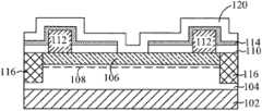
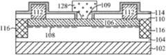
图1A和1B是根据本发明的一个或多个实施例的半导体结构100和101的截面图,每一个半导体结构都具有高电子迁移率晶体管(HEMT)。1A and 1B are cross-sectional views of
参照图1A,示出具有HEMT的半导体结构100。半导体结构100包括衬底102。在一些实施例中,衬底102包括碳化硅(SiC)衬底、蓝宝石衬底或者硅衬底。Referring to FIG. 1A , a
半导体结构100还包括在两个不同的半导体材料层(诸如具有不同带隙的材料层)之间形成的异质结。例如,半导体结构100包括非掺杂的窄带隙沟道层和宽带隙n型供给层。在至少一个实施例中,半导体结构100包括在衬底102上形成的第一III-V族化合物层(或者被称为沟道层)104和在沟道层104上形成的第二III-V族化合物层(或者被称为供给层)106。沟道层104和供给层106都是由元素周期表中的III-V族元素组成的化合物。但是,沟道层104和供给层106在组分上彼此不同。在至少一个实施例中,沟道层104是未掺杂的或者非故意掺杂的(UID)。在本实例的半导体衬底100中,沟道层104包括氮化镓(GaN)层(也被称为GaN层104)。供给层106包括氮化镓铝(AlGaN)层(也被称为AlGaN层106)。GaN层104和AlGaN层106相互直接接触。在另一实例中,沟道层104包括GaAs层或者InP层。供给层106包括AlGaAs层或者AlInP层。The
在一些实施例中,GaN层104是未掺杂的。在一些可选的实施例中,GaN层104是非故意掺杂的,诸如,由于用于形成GaN层104的前体具有轻掺杂的n型掺杂物。在一个实例中,GaN层104的厚度在约0.5微米至约10微米的范围内。In some embodiments,
在一些实施例中,AlGaN层106是故意掺杂的。在一个实例中,AlGaN层106的厚度在约5纳米(nm)至约50纳米的范围内。在至少一个实施例中,AlGaN层106包括AlxGa1-xN,其中x的范围为约0.15%至约100%。In some embodiments,
在AlGaN层106和GaN层104之间存在带隙不连续性。AlGaN层106中的来自压电效应的电子进入GaN层104中,在GaN层104中产生极薄的高迁移导电电子层108。该薄层108被称为二维电子气(2-DEG),形成载流子沟道(也被称为载流子沟道108)。2-DEG的薄层108位于AlGaN层106和GaN层104的界面处。因此,载流子沟道具有高电子迁移率,因为GaN层104是未掺杂的或者非故意掺杂的,因而电子可以自由运动而不与杂质碰撞或者基本上减少碰撞。There is a bandgap discontinuity between the
半导体结构100还包括设置在AlGaN层106上并且被配置用于电连接至载流子沟道108的源极部件和漏极部件。源极部件和漏极部件中的每一个都包括金属部件112。在一个实例中,金属部件112不包含Au而包含Al、Ti、Ni或者Cu。The
半导体结构100还包括设置在未被金属部件112占据的AlGaN层106的顶面上的介电覆盖层110。介电覆盖层110还包括暴露出用于栅电极形成的一部分AlGaN层106的开口。介电覆盖层100保护下面的AlGaN层106在使用等离子体的后续工艺中不受到损伤。The
在金属部件112和介电覆盖层110的顶面上设置保护层114。保护层114还包括与介电覆盖层110中的开口对准的开口。保护层114中的开口和介电覆盖层110中的开口的组合开口暴露出用于栅电极形成的部分AlGaN层106。A
半导体结构100还包括设置在保护层114中的开口和介电覆盖层110中的开口的组合开口的两个侧壁上的两个斜场板109。在一些实施例中,这些斜场板109可以由诸如Al2O3、Ta2O5、TiO2、ZnO2、HfO2等HI-K材料制成。The
半导体结构100还包括设置在源极和漏极部件之间的AlGaN层106上的组合开口上方的栅电极128。栅电极128包括被配置用于电压偏置并且与载流子沟道108电连接的导电材料层。在各个实例中,导电材料层可以包括难熔金属或者其化合物,例如钛(Ti)、氮化钛(TiN)、钛钨(TiW)、氮化钨(WN)、铜(Cu)和钨(W)。在该实施例中,栅电极128设置在部分保护层114、斜场板109和暴露出AlGaN层106的开口的上方。斜场板109的存在有助于降低一般发生在栅电极128底部边缘处的电场拥挤。The
半导体结构100还包括位于保护层114和介电覆盖层110中的组合开口下方的载流子沟道108中的耗尽区124。因为耗尽区124,载流子沟道108变成常关型(normally-off)。应当施加正栅极电压以导通这种HEMT的载流子沟道108。这种HEMT也被称为增强型HEMT,其与耗尽型HEMT不同。耗尽型HEMT具有常开型(normally-on)载流子沟道并且应当施加负栅极电压来断开载流子沟道。The
图1B是根据本发明的另一个实施例的具有HEMT的半导体结构101的截面图。半导体结构101的层堆叠件与图1A中示出的半导体结构100类似。但是,在该具体实施例中,不同于图1A中描述的实施例,进一步至少部分地去除位于两个斜场板109之间的部分AlGaN层106,以在AlGaN层106中形成沟槽,从而使一些栅电极材料128到达低于AlGaN层106的表面的水平面。在该结构101中,因为栅电极128的一部分进入AlGaN层106内,这增强了源极区和漏极区之间的电子转移。FIG. 1B is a cross-sectional view of a
在上述实施例中,栅电极128、源极/漏极部件以及GaN层104中的载流子沟道108被配置成晶体管。当对栅极堆叠件施加电压时,可以调制晶体管的器件电流。In the above-described embodiments, the
图2是根据本发明的一个或多个实施例形成具有HEMT的半导体结构的方法200的流程图。现参照图2方法200的流程图,在操作201中,提供第一III-V族化合物层。在衬底上形成第一III-V族化合物层。接下来,方法200继续到操作202,其中,在第一III-V族化合物层上外延生成第二III-V族化合物层。方法200继续到操作203,其中,在第二III-V族化合物层上形成源极部件和漏极部件。方法200继续到操作204,其中,在暴露出第二III-V族化合物层的组合开口的两个侧壁上形成斜场板109。方法200继续到操作205,其中,在源极部件和漏极部件之间的部分第二III-V族化合物层的上方形成栅电极。应当注意到,可以在图2的方法200之前、期间或者之后提供其他工艺。FIG. 2 is a flowchart of a
图3至图8是根据图2的方法200的各个实施例的在各个制造阶段的具有HEMT的半导体结构100的截面图。已将各个附图简化以便更好地理解本发明的发明构思。3-8 are cross-sectional views of the
参照图3,其是在实施操作201、202和203之后的半导体结构100的衬底102的一部分的放大截面图。在一些实施例中,衬底102包括碳化硅(SiC)衬底、蓝宝石衬底或者硅衬底。在衬底102上生长第一III-V族化合物层104,也被称为沟道层。在该实施例中,第一III-V族化合物层104是指氮化镓(GaN)层(也被称为GaN层104)。可以通过金属有机汽相外延(MOVPE)采用含镓前体和含氮前体外延生长GaN层104。含镓前体包括三甲基镓(TMG)、三乙基镓(TEG)或其他合适的化学物质。含氮前体包括氨(NH3)、叔丁胺(TBAm)、苯肼或其他合适的化学物质。GaN层104的厚度在约0.5微米至约10微米的范围内。在其他实施例中,第一III-V族化合物层104可以包括GaAs层或者InP层。Referring to FIG. 3 , which is an enlarged cross-sectional view of a portion of
在第一III-V族化合物层104上生长第二III-V族化合物层106,其也被称为供给层。在第一III-V族化合物层104和第二III-V族化合物层106之间限定出界面。二维电子气(2-DEG)载流子沟道108位于界面处。在至少一个实施例中,第二III-V族化合物层106是指氮化镓铝(AlGaN)层(也被称为AlGaN层106)。可以通过MOVPE采用含铝前体、含镓前体和含氮前体在GaN层104上外延生长AlGaN层106。含铝前体包括三甲基铝(TMA)、三乙基铝(TEA)或其他合适的化学物质。含镓前体包括TMG、TEG或其他合适的化学物质。含氮前体包括氨、TBAm、苯肼或其他合适的化学物质。AlGaN层106的厚度在约5纳米至约50纳米的范围内。在一些实施例中,第二III-V族化合物层106可以包括AlGaAs层或者AlInP层。On the first III-
在第二III-V族化合物层106的顶面107上沉积介电覆盖层110。介电覆盖层110的厚度在约
金属层设置在介电覆盖层110的上方,过填充(overfill)开口并且接触第二III-V族化合物层106。在金属层上方形成光刻胶层(未示出)并且使其显影以在开口上方形成部件。通过反应离子蚀刻(RIE)工艺去除未被光刻胶层的部件覆盖的金属层,反应离子蚀刻(RIE)工艺向下蚀刻金属层的暴露部分至下面的介电覆盖层110。在蚀刻工艺之后形成金属部件112。金属部件112被配置作为用于HEMT的源极部件或者漏极部件。在形成金属部件112之后去除光刻胶层。介电覆盖层110保护下面的第二III-V族化合物层106在用于形成金属部件112的蚀刻工艺期间不受到损伤。位于第二III-V族化合物层106下面的2-DEG载流子沟道108中的载流子不会受到影响。半导体结构101的电气性能会受到正面影响。从而,整个组件的产率会增加。A metal layer is disposed over the
金属部件112的金属层可以包括一种或多种导电材料。在至少一个实例中,金属层不包含金(Au)而包含钛(Ti)、氮化钛(TiN)或者铝铜(AlCu)合金。在另一实例中,金属层包括底部Ti/TiN层、位于底部Ti/TiN层上面的AlCu层、以及位于AlCu层上面的顶部Ti层。金属层的形成方法包括原子层沉积(ALD)或者物理汽相沉积(PVD)工艺。在金属部件112中不使用Au的情况下,也可以将方法200应用于在硅衬底上生产集成电路的生产线中。可以消除Au对硅制造工艺的污染问题。The metal layer of
接下来,在金属部件112以及介电覆盖层110的顶面上沉积保护层114。保护层114可以包括诸如SiO2或者Si3N4的介电材料。在一个实例中,保护层114是Si3N4并且通过实施等离子体增强化学汽相沉积(PECVD)方法形成。Next, a
图4示出在第一III-V族化合物层104和第二III-V族化合物层106中形成隔离区116之后的结构100。隔离区116将结构100中的HEMT与衬底102中的其他器件隔离开。在一个实例中,通过注入工艺采用氧或者氮种类形成隔离区116。保护层114保护源极部件和漏极部件在注入工艺之后的退火工艺期间不被暴露出来。FIG. 4 shows
图5示出在保护层114和介电覆盖层110中形成开口118之后的结构100。在保护层114的顶面上形成经图案化的掩模层(未示出)并且实施蚀刻工艺以去除保护层114和介电覆盖层110的一部分。开口118暴露出第二III-V族化合物层106的顶面107的一部分。开口118被配置为随后形成栅电极的位置。FIG. 5 shows
图6示出如何在开口118的两侧上沉积两个斜场板109。为了形成斜场板109,首先在开口118的上方设置预期用于形成斜场板109的材料层120。在至少一个实施例中,该层120的厚度等于保护层114和介电覆盖层110的厚度总和。在一些实施例中,在该沉积步骤之后,层120填充整个开口118。FIG. 6 shows how two
接下来,如图7中所描述的,实施诸如干法蚀刻的去除工艺以去除部分层120。具体而言,蚀刻工艺开始于去除位于保护层114上方和开口118内部的整个层120。去除工艺(即蚀刻工艺)继续直到其到达保护层114。因此,保护层114基本上充当蚀刻终止层。作为在保护层114处终止去除工艺的结果,已经去除了位于保护层114顶上和开口118外面的层120的所有部分。因为开口118中的层120的一些部分低于保护层114,当蚀刻工艺终止时,层120的一些部分仍保留在开口118中。位于开口118中的层120的这些剩余部分将在开口118的侧壁上形成两个三角形状的板,这两个三角形状的板成为斜场板109。Next, as described in FIG. 7 , a removal process such as dry etching is performed to remove a portion of
根据如图1B所述的本发明的另一个实施例,半导体结构与上面论述的先前实施例中的结构100基本上相同,除了在该实施例中已在开口118中形成斜场板109之后,实施另外的蚀刻工艺去除一些暴露的AlGaN层106。该另外的蚀刻步骤在低于AlGaN层106原表面的AlGaN层106中形成沟槽121。According to another embodiment of the present invention as illustrated in FIG. 1B , the semiconductor structure is substantially the same as the
图8示出在实施操作205之后的结构100,其在耗尽区124上方的部分第二III-V族化合物层106的上方形成栅电极128。在一个实例中,在部分保护层114的上方形成栅电极128,并且栅电极128覆盖整个开口118,包括两个斜场板109。载流子沟道108的耗尽区124中的电子在操作204中的沉积工艺期间被耗尽。在该实例中,沉积栅电极层并且过填充图7中示出的开口118。对栅电极层实施光刻和蚀刻工艺以限定出源极和漏极部件之间的栅电极128。栅电极128包括导电材料层,其可以包括难熔金属或者其化合物,例如钛(Ti)、氮化钛(TiN)、钛钨(TiW)、氮化钨(WN)和钨(W)。在另一实例中,栅电极128可以包括镍(Ni)、金(Au)或者铜(Cu)。FIG. 8 shows
注意到在上面所有的实施例中,可以通过图3至图8和相关文本示出的工艺形成具有HEMT的结构100。用于形成具有HEMT的结构101的工艺与形成结构100类似,除了在开口118的侧壁上形成斜场板109之后,进一步蚀刻暴露出的部分AlGaN层106以形成沟槽。在图8中,在开口内沉积栅电极材料128以填充整个开口118和沟槽。鉴于此,形成了具有增强型HEMT的结构101。Note that in all of the above embodiments, the
本发明的各个实施例可以用于改进具有高电子迁移率晶体管(HEMT)的半导体结构的性能。例如,在常规方法中,蚀刻第二III-V族化合物层的一部分以形成用于增强型HEMT的凹槽。在蚀刻凹槽期间,难以控制同一衬底上的半导体芯片区之间的蚀刻一致性。可能不能准确地控制在同一半导体芯片区或者同一衬底中的每个HEMT的电气性能。在一些实施例中,金属部件112不包含Au而包含Al、Ti或者Cu。在金属部件112中不使用Au的情况下,方法200也可以应用于在硅衬底上生产集成电路的生产线。可以消除Au对硅制造工艺中的污染问题。与在源极/漏极部件中具有Au的HEMT相比,制造根据本申请的HEMT的成本降低了。可以在同一生产线中应用III-V族半导体化合物工艺和硅制造工艺。其增加了对生产线分配不同产品的灵活性。Various embodiments of the present invention may be used to improve the performance of semiconductor structures having high electron mobility transistors (HEMTs). For example, in a conventional method, a portion of the second III-V compound layer is etched to form a recess for an enhancement mode HEMT. During etching of grooves, it is difficult to control etch uniformity between semiconductor chip regions on the same substrate. It may not be possible to accurately control the electrical performance of each HEMT in the same semiconductor chip area or the same substrate. In some embodiments,
根据本发明的一个实施例,一种半导体结构包括第一III-V族化合物层。第二III-V族化合物层设置在第一III-V族化合物层上并且在组分上不同于第一III-V族化合物层。载流子沟道位于第一III-V族化合物层和第二III-V族化合物层之间。源极部件和漏极部件设置在第二III-V族化合物层上。栅电极设置在源极部件和漏极部件之间的第二III-V族化合物层的上方。两个斜场板设置在位于第二III-V族化合物层上的保护层中的开口和介电覆盖层中的开口的组合开口的两个侧壁上。According to one embodiment of the present invention, a semiconductor structure includes a first III-V compound layer. The second group III-V compound layer is disposed on the first group III-V compound layer and is compositionally different from the first group III-V compound layer. The carrier channel is located between the first III-V compound layer and the second III-V compound layer. A source feature and a drain feature are disposed on the second III-V compound layer. A gate electrode is disposed over the second III-V compound layer between the source feature and the drain feature. Two slope field plates are disposed on both sidewalls of the combined opening of the opening in the protective layer and the opening in the dielectric cap layer on the second III-V compound layer.
根据本发明的另一个实施例,一种半导体结构包括设置在衬底上的GaN层。AlGaN层设置在GaN层上。载流子沟道位于GaN层和AlGaN层之间。间隔分开的源极部件和漏极部件设置在AlGaN层上。栅电极设置在源极部件和漏极部件之间的AlGaN层的上方。载流子沟道耗尽层的一部分设置在栅电极和AlGaN层之间。两个斜场板设置在位于第二III-V族化合物层上的保护层中的开口和介电覆盖层中的开口的组合开口的两个侧壁上。According to another embodiment of the present invention, a semiconductor structure includes a GaN layer disposed on a substrate. An AlGaN layer is provided on the GaN layer. The carrier channel is located between the GaN layer and the AlGaN layer. Spaced apart source and drain features are disposed on the AlGaN layer. A gate electrode is disposed over the AlGaN layer between the source feature and the drain feature. A portion of the carrier channel depletion layer is provided between the gate electrode and the AlGaN layer. Two slope field plates are disposed on both sidewalls of the combined opening of the opening in the protective layer and the opening in the dielectric cap layer on the second III-V compound layer.
本发明还描述形成半导体结构的方法的实施例。方法包括提供第一III-V族化合物层。在第一III-V族化合物层上外延生长第二III-V族化合物层。载流子沟道位于第一III-V族化合物层和第二III-V族化合物层之间。在第二III-V族化合物层上形成源极部件和漏极部件。在设置在第二III-V族化合物层上的保护层中的开口和介电覆盖层中的开口的组合开口的两个侧壁上设置两个斜场板。在源极部件和漏极部件之间的部分第二III-V族化合物层的上方形成栅电极。Embodiments of methods of forming semiconductor structures are also described herein. The method includes providing a first III-V compound layer. A second III-V compound layer is epitaxially grown on the first III-V compound layer. The carrier channel is located between the first III-V compound layer and the second III-V compound layer. Source features and drain features are formed on the second III-V compound layer. Two slope field plates are disposed on both sidewalls of the combined opening of the opening in the protective layer and the opening in the dielectric capping layer disposed on the second III-V compound layer. A gate electrode is formed over a portion of the second III-V compound layer between the source feature and the drain feature.
尽管已经详细地描述了实施例及其优势,但应该理解,可以在不背离所附权利要求限定的本发明的精神和范围的情况下,在其中进行各种改变、替换和更改。而且,本申请的范围并不限于本说明书中描述的工艺、机器、制造、材料组分、装置、方法和步骤的特定实施例。作为本领域普通技术人员根据本发明的公开内容将很容易地理解,根据本发明可以利用现有的或今后开发的用于执行与本文所述相应实施例基本上相同的功能或者获得基本上相同的结果的工艺、机器、制造、材料组分、装置、方法或步骤。因此,所附权利要求预期在其范围内包括这样的工艺、机器、制造、材料组分、装置、方法或步骤。Although the embodiments and their advantages have been described in detail, it should be understood that various changes, substitutions and alterations can be made herein without departing from the spirit and scope of the invention as defined by the appended claims. Moreover, the scope of the present application is not limited to the particular embodiments of the process, machine, manufacture, composition of matter, means, methods and steps described in the specification. Those of ordinary skill in the art will readily understand from the disclosure of the present invention that existing or future developed devices for performing substantially the same functions as the corresponding embodiments described herein or to obtain substantially the same functions can be utilized according to the present invention. A process, machine, manufacture, composition of material, means, method or step that results in a result. Accordingly, the appended claims are intended to include within their scope such processes, machines, manufacture, compositions of matter, means, methods, or steps.
Claims (10)
Translated fromChineseApplications Claiming Priority (2)
| Application Number | Priority Date | Filing Date | Title |
|---|---|---|---|
| US13/403,686 | 2012-02-23 | ||
| US13/403,686US8860088B2 (en) | 2012-02-23 | 2012-02-23 | Semiconductor structure and method of forming the same |
Publications (2)
| Publication Number | Publication Date |
|---|---|
| CN103296077Atrue CN103296077A (en) | 2013-09-11 |
| CN103296077B CN103296077B (en) | 2016-08-03 |
Family
ID=49001869
Family Applications (1)
| Application Number | Title | Priority Date | Filing Date |
|---|---|---|---|
| CN201210525310.6AActiveCN103296077B (en) | 2012-02-23 | 2012-12-07 | Semiconductor structure and forming method thereof |
Country Status (2)
| Country | Link |
|---|---|
| US (3) | US8860088B2 (en) |
| CN (1) | CN103296077B (en) |
Cited By (1)
| Publication number | Priority date | Publication date | Assignee | Title |
|---|---|---|---|---|
| WO2019114837A1 (en)* | 2017-12-15 | 2019-06-20 | 苏州能讯高能半导体有限公司 | Semiconductor device and manufacturing method thereof |
Families Citing this family (10)
| Publication number | Priority date | Publication date | Assignee | Title |
|---|---|---|---|---|
| EP2930754A1 (en) | 2014-04-11 | 2015-10-14 | Nxp B.V. | Semiconductor device |
| CN106847895B (en)* | 2016-12-14 | 2019-10-11 | 西安电子科技大学 | GaN-based high electron mobility transistor based on TiN/Cu/Ni gate electrode and manufacturing method |
| JP2019165056A (en)* | 2018-03-19 | 2019-09-26 | 住友電気工業株式会社 | Method for manufacturing semiconductor device |
| CN110120347B (en)* | 2018-02-05 | 2023-11-17 | 住友电气工业株式会社 | Method for forming field effect transistor |
| US10692857B2 (en)* | 2018-05-08 | 2020-06-23 | Vanguard International Semiconductor Corporation | Semiconductor device combining passive components with HEMT |
| US11127847B2 (en)* | 2019-05-16 | 2021-09-21 | Vanguard International Semiconductor Corporation | Semiconductor devices having a gate field plate including an extension portion and methods for fabricating the semiconductor device |
| CN112349773A (en)* | 2019-08-07 | 2021-02-09 | 苏州能讯高能半导体有限公司 | Semiconductor device and preparation method thereof |
| US12408403B2 (en) | 2020-10-27 | 2025-09-02 | Macom Technology Solutions Holdings, Inc. | Field effect transistor with stacked unit subcell structure |
| US12266721B2 (en) | 2020-10-27 | 2025-04-01 | Wolfspeed, Inc. | Field effect transistor with multiple stepped field plate |
| US11502178B2 (en)* | 2020-10-27 | 2022-11-15 | Wolfspeed, Inc. | Field effect transistor with at least partially recessed field plate |
Citations (3)
| Publication number | Priority date | Publication date | Assignee | Title |
|---|---|---|---|---|
| US5391899A (en)* | 1991-10-29 | 1995-02-21 | Mitsubishi Denki Kabushiki Kaisha | Compound semiconductor device with a particular gate structure |
| US7906799B2 (en)* | 2004-01-16 | 2011-03-15 | Cree, Inc. | Nitride-based transistors with a protective layer and a low-damage recess |
| CN102171830A (en)* | 2008-07-31 | 2011-08-31 | 克里公司 | Normally-off semiconductor devices and methods of fabricating the same |
Family Cites Families (10)
| Publication number | Priority date | Publication date | Assignee | Title |
|---|---|---|---|---|
| JPH05343374A (en)* | 1992-06-05 | 1993-12-24 | Hitachi Ltd | Compound semiconductor processing method and processing apparatus |
| WO2006001369A1 (en)* | 2004-06-24 | 2006-01-05 | Nec Corporation | Semiconductor device |
| US20070018199A1 (en)* | 2005-07-20 | 2007-01-25 | Cree, Inc. | Nitride-based transistors and fabrication methods with an etch stop layer |
| US8936976B2 (en)* | 2009-12-23 | 2015-01-20 | Intel Corporation | Conductivity improvements for III-V semiconductor devices |
| JP2012054471A (en)* | 2010-09-02 | 2012-03-15 | Fujitsu Ltd | Semiconductor device, method of manufacturing the same, and power supply device |
| US8357571B2 (en)* | 2010-09-10 | 2013-01-22 | Cree, Inc. | Methods of forming semiconductor contacts |
| US8772842B2 (en)* | 2011-03-04 | 2014-07-08 | Transphorm, Inc. | Semiconductor diodes with low reverse bias currents |
| US8716141B2 (en)* | 2011-03-04 | 2014-05-06 | Transphorm Inc. | Electrode configurations for semiconductor devices |
| US9018677B2 (en)* | 2011-10-11 | 2015-04-28 | Taiwan Semiconductor Manufacturing Company, Ltd. | Semiconductor structure and method of forming the same |
| US20130105817A1 (en)* | 2011-10-26 | 2013-05-02 | Triquint Semiconductor, Inc. | High electron mobility transistor structure and method |
- 2012
- 2012-02-23USUS13/403,686patent/US8860088B2/enactiveActive
- 2012-12-07CNCN201210525310.6Apatent/CN103296077B/enactiveActive
- 2014
- 2014-08-21USUS14/465,250patent/US9425300B2/ennot_activeExpired - Fee Related
- 2016
- 2016-08-22USUS15/242,881patent/US10115813B2/enactiveActive
Patent Citations (3)
| Publication number | Priority date | Publication date | Assignee | Title |
|---|---|---|---|---|
| US5391899A (en)* | 1991-10-29 | 1995-02-21 | Mitsubishi Denki Kabushiki Kaisha | Compound semiconductor device with a particular gate structure |
| US7906799B2 (en)* | 2004-01-16 | 2011-03-15 | Cree, Inc. | Nitride-based transistors with a protective layer and a low-damage recess |
| CN102171830A (en)* | 2008-07-31 | 2011-08-31 | 克里公司 | Normally-off semiconductor devices and methods of fabricating the same |
Cited By (1)
| Publication number | Priority date | Publication date | Assignee | Title |
|---|---|---|---|---|
| WO2019114837A1 (en)* | 2017-12-15 | 2019-06-20 | 苏州能讯高能半导体有限公司 | Semiconductor device and manufacturing method thereof |
Also Published As
| Publication number | Publication date |
|---|---|
| US8860088B2 (en) | 2014-10-14 |
| US20130221364A1 (en) | 2013-08-29 |
| US20160359035A1 (en) | 2016-12-08 |
| US9425300B2 (en) | 2016-08-23 |
| US10115813B2 (en) | 2018-10-30 |
| US20140361310A1 (en) | 2014-12-11 |
| CN103296077B (en) | 2016-08-03 |
Similar Documents
| Publication | Publication Date | Title |
|---|---|---|
| US10157994B2 (en) | High electron mobility transistor and method of forming the same | |
| US10325910B2 (en) | Semiconductor device containing HEMT and MISFET and method of forming the same | |
| CN103296077B (en) | Semiconductor structure and forming method thereof | |
| US9748372B2 (en) | Semiconductor structure and method of forming the same | |
| US9236465B2 (en) | High electron mobility transistor and method of forming the same | |
| CN102881720B (en) | Semiconductor structure and forming method thereof | |
| CN103545360B (en) | HEMT and forming method thereof | |
| US8624296B1 (en) | High electron mobility transistor including an embedded flourine region | |
| CN103050511B (en) | Semiconductor structure and the method forming semiconductor structure | |
| CN107170818A (en) | Semiconductor devices |
Legal Events
| Date | Code | Title | Description |
|---|---|---|---|
| C06 | Publication | ||
| PB01 | Publication | ||
| C10 | Entry into substantive examination | ||
| SE01 | Entry into force of request for substantive examination | ||
| C14 | Grant of patent or utility model | ||
| GR01 | Patent grant |