CN103293761A - Display device - Google Patents
Display deviceDownload PDFInfo
- Publication number
- CN103293761A CN103293761ACN2012100432006ACN201210043200ACN103293761ACN 103293761 ACN103293761 ACN 103293761ACN 2012100432006 ACN2012100432006 ACN 2012100432006ACN 201210043200 ACN201210043200 ACN 201210043200ACN 103293761 ACN103293761 ACN 103293761A
- Authority
- CN
- China
- Prior art keywords
- display device
- light
- guide plate
- main body
- light guide
- Prior art date
- Legal status (The legal status is an assumption and is not a legal conclusion. Google has not performed a legal analysis and makes no representation as to the accuracy of the status listed.)
- Granted
Links
Images


Landscapes
- Planar Illumination Modules (AREA)
Abstract
Translated fromChinese
Description
Translated fromChinese技术领域technical field
本发明涉及一种显示装置,特别是涉及一种包括导光板的显示装置。The present invention relates to a display device, in particular to a display device including a light guide plate.
背景技术Background technique
已知的显示装置包括导光板、配置在导光板一侧的多个发光元件、位于导光板上的显示面板以及共同挟持显示面板及导光板的边框与背板。在已知技术中,导光板在接近发光元件处易发生光束分布不均的问题。因此,已知的显示装置利用边框遮蔽光束分布不均的区域,而使得边框的窄化受到限制。已知的显示装置还包括用以驱动显示面板及发光元件的二块驱动电路板。这些驱动电路板多设在背板后方,而使得整体显示装置的厚度不易下降。A known display device includes a light guide plate, a plurality of light emitting elements disposed on one side of the light guide plate, a display panel located on the light guide plate, and a frame and a back plate that jointly hold the display panel and the light guide plate. In the known technology, the light guide plate is prone to the problem of uneven distribution of light beams near the light emitting elements. Therefore, the known display device utilizes the frame to shield the region where the beam distribution is uneven, so that the narrowing of the frame is limited. The known display device also includes two driving circuit boards for driving the display panel and the light emitting elements. These driving circuit boards are mostly disposed behind the backplane, so that the thickness of the overall display device is not easily reduced.
中国台湾专利M284913揭露了一种背光模组。此背光模组包括导光板。此导光板的侧边设置有凸块。中国台湾专利I331666揭露了一种导光板。此导光板的条状侧面上具有多个光学微结构。中国台湾专利公开第201017291号揭露了一种导光板。此导光板的侧边具有多个光学微结构。这些光学微结构可具有多个弧面。中国专利CN102121622A揭露了一种直下式背光模组。此背光模组包括导光板、多个光源及光学胶。Chinese Taiwan Patent M284913 discloses a backlight module. The backlight module includes a light guide plate. The side of the light guide plate is provided with bumps. Chinese Taiwan patent I331666 discloses a light guide plate. There are multiple optical microstructures on the strip-shaped side of the light guide plate. China Taiwan Patent Publication No. 201017291 discloses a light guide plate. The side of the light guide plate has multiple optical microstructures. These optical microstructures can have multiple curved surfaces. Chinese patent CN102121622A discloses a direct type backlight module. The backlight module includes a light guide plate, multiple light sources and optical glue.
发明内容Contents of the invention
本发明提供一种显示装置,其具有窄边框宽度。The invention provides a display device with a narrow frame width.
本发明的其他目的和优点可以从本发明所揭露的技术特征中得到进一步的了解。Other purposes and advantages of the present invention can be further understood from the technical features disclosed in the present invention.
为达上述之一或部分或全部目的或是其他目的,本发明的一个实施例提出一种显示装置,其包括导光板、至少一发光元件、边框以及显示面板。导光板包括主体以及至少一入光凸部。主体具有出光面。入光凸部与主体连接且具有入光面。发光元件沿着入光面配置且用于发出光束。光束自入光面进入导光板中且经由出光面离开导光板。边框配置在导光板上。显示面板位于导光板与边框之间。边框以及显示面板曝露出入光凸部。To achieve one or part or all of the above objectives or other objectives, an embodiment of the present invention provides a display device, which includes a light guide plate, at least one light emitting element, a frame and a display panel. The light guide plate includes a main body and at least one light incident protrusion. The main body has a light-emitting surface. The light incident convex part is connected with the main body and has a light incident surface. The light emitting element is arranged along the light incident surface and is used for emitting light beams. The light beam enters the light guide plate from the light incident surface and leaves the light guide plate through the light exit surface. The frame is configured on the light guide plate. The display panel is located between the light guide plate and the frame. The frame and the display panel expose the light-incident convex portion.
基于上述,本发明的实施例可达到下列优点的至少一种。在本发明的一个实施例的显示装置中,由于发光元件所发出的光束可在边框之外的入光凸部进行混光,因此边框可不需遮蔽易发生光束分布不均问题的混光区(即入光凸部所在的区域)。如此一来,边框的宽度便可设计地较窄,进而实现窄边框的显示装置。Based on the above, the embodiments of the present invention can achieve at least one of the following advantages. In the display device according to an embodiment of the present invention, since the light beam emitted by the light-emitting element can be mixed in the light-incident convex portion outside the frame, the frame does not need to cover the light-mixing area ( That is, the area where the light incident convex part is located). In this way, the width of the bezel can be designed to be narrow, thereby realizing a display device with a narrow bezel.
为让本发明的上述特征和优点能更明显易懂,下文特举实施例,并配合附图式作详细说明如下。In order to make the above-mentioned features and advantages of the present invention more comprehensible, the following specific embodiments are described in detail with accompanying drawings.
附图说明Description of drawings
图1为本发明第一实施例的显示装置的立体示意图。FIG. 1 is a schematic perspective view of a display device according to a first embodiment of the present invention.
图2为图1的显示装置的主视图。FIG. 2 is a front view of the display device of FIG. 1 .
图3为根据图2的剖线A-A’所示的剖面图。Fig. 3 is a sectional view according to the section line A-A' of Fig. 2 .
图4示出图2的边框、显示面板、导光板以及发光元件。FIG. 4 shows the frame, the display panel, the light guide plate and the light emitting element of FIG. 2 .
图5A示出图4的导光板及反射片。FIG. 5A shows the light guide plate and the reflection sheet of FIG. 4 .
图5B及图5C示出图5A的局部区域。5B and 5C show partial areas of FIG. 5A.
图6示出本发明另一实施例的导光板。FIG. 6 shows a light guide plate according to another embodiment of the present invention.
图7示出本发明又一实施例的导光板。Fig. 7 shows a light guide plate according to another embodiment of the present invention.
图8示出本发明再一实施例的导光板。FIG. 8 shows a light guide plate according to yet another embodiment of the present invention.
图9示出本发明一实施例的导光板。FIG. 9 shows a light guide plate according to an embodiment of the present invention.
图10示出本发明另一实施例的导光板。FIG. 10 shows a light guide plate according to another embodiment of the present invention.
图11示出本发明又一实施例的导光板。Fig. 11 shows a light guide plate according to another embodiment of the present invention.
图12示出本发明再一实施例的导光板。Fig. 12 shows a light guide plate according to another embodiment of the present invention.
图13示出本发明一实施例的导光板。Fig. 13 shows a light guide plate according to an embodiment of the present invention.
图14示出本发明另一实施例的导光板。Fig. 14 shows a light guide plate according to another embodiment of the present invention.
图15示出本发明再一实施例的导光板。Fig. 15 shows a light guide plate according to another embodiment of the present invention.
图16示出图1的显示装置的背面。FIG. 16 shows the back side of the display device of FIG. 1 .
图17为本发明第二实施例的显示装置的立体示意图。FIG. 17 is a schematic perspective view of a display device according to a second embodiment of the present invention.
图18为根据图17的剖线B-B’所示的剖面图。Fig. 18 is a sectional view according to the section line B-B' of Fig. 17 .
图19示出图18的导光板、显示面板与边框。FIG. 19 shows the light guide plate, display panel and frame of FIG. 18 .
图20示出本发明一实施例的导光板。FIG. 20 shows a light guide plate according to an embodiment of the present invention.
图21示出本发明另一实施例的导光板。Fig. 21 shows a light guide plate according to another embodiment of the present invention.
图22示出本发明又一实施例的导光板。Fig. 22 shows a light guide plate according to another embodiment of the present invention.
【主要元件符号说明】[Description of main component symbols]
100、100A:显示装置100, 100A: display device
110、110A~110N:导光板110, 110A~110N: light guide plate
112:主体112: subject
112a:出光面112a: Light-emitting surface
112b:第二周面112b: Second week surface
112c:第三光学微结构112c: The third optical microstructure
114:入光凸部114: light incident convex part
114a:入光面114a: light incident surface
114b:第一光学微结构114b: the first optical microstructure
114c:第一周面114c: The first week
114d:第二光学微结构114d: Second optical microstructure
120:发光元件120: light emitting element
130:边框130: border
140:显示面板140: display panel
142:显示区142: display area
150:背板150: Backplane
160:反射片160: reflector
170:基座170: Pedestal
180:第一连接件180: first connector
182:第二连接件182: Second connector
190:第一驱动电路板190: The first drive circuit board
192:第二驱动电路板192: Second drive circuit board
194:转轴194: Shaft
195:主机模块195: host module
A、B、C、D、E、F、W1:宽度A, B, C, D, E, F, W1: Width
C3:第三弧面C3: third arc surface
C4:第四弧面C4: the fourth arc
D:厚度D: Thickness
L1、L2、L2’、L2”、L3:光束L1, L2, L2’, L2”, L3: light beams
S1:第一表面S1: first surface
S2:第二表面S2: second surface
S3:第三表面S3: third surface
S4:第四表面S4: fourth surface
P1:第一斜面P1: first slope
P2:第二斜面P2: second slope
P3:第三斜面P3: third slope
P4:第四斜面P4: the fourth slope
X:参考轴X: reference axis
具体实施方式Detailed ways
有关本发明的前述及其他技术内容、特点与功效,在以下配合参考图式的一较佳实施例的详细说明中,将可清楚的呈现。以下实施例中所提到的方向用语,例如:上、下、左、右、前或后等,仅是参考附加图式的方向。因此,使用的方向用语是用来说明并非用来限制本发明。The aforementioned and other technical contents, features and effects of the present invention will be clearly presented in the following detailed description of a preferred embodiment with reference to the drawings. The directional terms mentioned in the following embodiments, such as: up, down, left, right, front or back, etc., are only directions referring to the attached drawings. Accordingly, the directional terms are used to illustrate and not to limit the invention.
第一实施例first embodiment
图1为本发明第一实施例的显示装置的立体示意图。图2为图1的显示装置的主视图。图3为根据图2的剖线A-A’所示的剖面图。请参照图1、图2及图3,本实施例的显示装置100包括导光板110(示于图3)、至少一发光元件120(示于图3)、边框130以及显示面板140。在本实施例中,显示面板140可为非自发光显示面板,例如液晶显示面板,但本发明不限于此。FIG. 1 is a schematic perspective view of a display device according to a first embodiment of the present invention. FIG. 2 is a front view of the display device of FIG. 1 . Fig. 3 is a sectional view according to the section line A-A' of Fig. 2 . Referring to FIG. 1 , FIG. 2 and FIG. 3 , the
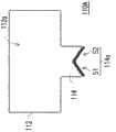
图4绘出图2的边框、显示面板、导光板以及发光元件。请参照图3及图4,本实施例的导光板110包括主体112以及至少一入光凸部114。主体112具有出光面112a。入光凸部114与主体112连接且具有入光面114a。如图3所示,在本实施例中,主体112与入光凸部114基本上可位于同一平面。本实施例的发光元件120沿着入光面114a配置且用于发出光束(未示出)。此光束自入光面114a进入导光板110中且经由出光面112a离开导光板110。在本实施例中,发光元件120例如为发光二极管。但本发明不限于此,在其他实施例中,发光元件120亦可为其他适当的光源。FIG. 4 depicts the frame, the display panel, the light guide plate and the light emitting element of FIG. 2 . Referring to FIG. 3 and FIG. 4 , the
值得注意是,如图4所示,在本实施例中,导光板110的主体112的宽度A大于入光凸部114的宽度为B。举例而言,导光板110的主体112的宽度A与入光凸部114的宽度B可满足下式(1)。It should be noted that, as shown in FIG. 4 , in this embodiment, the width A of the
请继续参照图3及图4,本实施例的边框130配置在导光板110上。本实施例的显示面板140位于导光板110与边框130之间。更进一步的说,本实施例的边框130覆盖显示面板140的边缘及导光板110的部分边缘,并曝露出显示面板140的显示区142。如图3所示,本实施例的显示装置100可进一步包括背板150。边框130与背板150可共同挟持显示面板140及导光板110。Please continue to refer to FIG. 3 and FIG. 4 , the
值得一提的是,在本实施例中,边框130以及显示面板140曝露出导光板110的入光凸部114。换言之,至少部分的入光凸部114是在边框130之外。各发光元件120所发出的光束(未示出)可先在边框130之外的入光凸部114进行混光作用,然后再进入主体112中,进而避免光束在主体112处发生分布不均的问题。由于光束是在边框130之外的入光凸部114中进行混光,因此本实施例的边框130不需遮蔽易发生光束分布不均问题的混光区门入光凸部114所在的区域)。这样一来,边框130的宽度W1(示于图4)便可设计地较窄,进而实现窄边框的显示装置100。It is worth mentioning that, in this embodiment, the
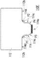
请参照图4,本实施例的导光板110的入光面114a可具有多个第一光学微结构114b。第一光学微结构114b用以使入射至入光面114a的光束产生散射。换言之,第一光学微结构114b可使发光元件120所发出的光束有效地分散至入光凸部114各处。在本实施例中,这些第一光学微结构114b例如为彼此连接的多个V形凹槽。这些V形凹槽的延伸方向可与出光面112a垂直。然而,第一光学微结构114b的形式并不限于V形凹槽,其他可使光束发生散射的光学结构亦可做为本实施例的第一光学微结构114b。Referring to FIG. 4 , the
本实施例的入光凸部114还具有连接入光面114a与主体112的第一周面114c。第一周面114c可具有多个第二光学微结构114d。本实施例的主体112还具有第二周面112b。第二周面112b环绕出光面112a且连接入光面114a与出光面112a。第二周面112b可具有多个第三光学微结构112c。第二光学微结构114d与第三光学微结构112c分别用以将传递至第一周面114c及第二周面112b的光束引导回入光凸部114的内部及主体112的内部。The light incident
在本实施例中,第二光学微结构114d的外形可与第三光学微结构112c的外形相同。但本发明不限于此,在其他实施例中,第二光学微结构114d的外形亦可与第三光学微结构112c的外形不同。本实施例的第二光学微结构114d(及第三光学微结构112c)可为彼此连接的多个弧形凹槽,而这些弧形凹槽的延伸方向可与出光面112a垂直。然而,第二光学微结构114d的形式(及第三光学微结构112c的形式)并不限于弧形凹槽,其他可引导光束重新回到导光板110内部的光学微结构亦可做为本实施例的第二光学微结构114d(及第三光学微结构112c)。In this embodiment, the shape of the second
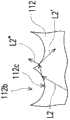
以下配合图5A、图5B及图5C详细说明第三光学微结构112c将光束引导回主体112的内部的机制。图5A示出图4的导光板及反射片。图5B及图5C示出图5A的局部区域。请参照图5A,本实施例的显示装置100可进一步包括反射片160。反射片160可环设在导光板110旁。更进一步地说,反射片160可配置在第一周面114c与第二周面112b旁且曝露出入光面114a。与参考轴X夹角小的光束L1传递至第三光学微结构112c后可穿过第三光学微结构112c,进而被反射片160反射回主体112内部。请参照图5B,与参考轴X夹角次小的光束L2传递至第三光学微结构112c后可被反射至相邻的另一第三光学微结构112c,部分光束L2’会被相邻的另一第三光学微结构112c反射回主体112内部。另一部分的光束L2”会穿过相邻的另一第三光学微结构112c,进而被反射片160反射回主体112内部。请参照图5C,与参考轴X夹角较大的光束L3传递至第三光学微结构112c后可被反射至相邻的另一第三光学微结构112c,进而被此第三光学微结构112c反射回主体112内部。第二光学微结构114d的作用机制与第三光学微结构112c类似便不再重述。The mechanism by which the third
请再参照图4,在本实施例中,入光凸部114的外轮廓大致上可呈长方体,而入光面114a大致上可呈一平面。然而,本发明的入光面114a的外形不限于图4中所示。入光面114a的形式可视实际的需求做适当的调整。以下配合图6至图12举例说明。Referring to FIG. 4 again, in this embodiment, the outer contour of the light-incident
图6示出本发明另一实施例的导光板。请参照图6,在导光板110A中,入光面114a可朝向主体112凹陷。详言之,入光面114a包括第一表面S1以及与第一表面S1直接连接的第二表面S2。第一表面S1以及第二表面S2与出光面112a垂直。第一表面S1与第二表面S2形成凹陷,此凹陷凹向主体112。换言之,在导光板110A中,入光面114a可为凹向主体112的V形凹槽。FIG. 6 shows a light guide plate according to another embodiment of the present invention. Referring to FIG. 6 , in the
图7示出本发明又一实施例的导光板。请参照图7,在导光板110B中,入光面114a可为第一弧面。此第一弧面可凹向主体112。换言之,在导光板110B中,入光面114a可为凹向主体112的弧形凹槽。Fig. 7 shows a light guide plate according to another embodiment of the present invention. Referring to FIG. 7 , in the
图8示出本发明再一实施例的导光板。请参照图8,在导光板110C中,入光面114a可朝向远离主体112的方向凸起。详言之,在导光板110C中,入光面114a包括第三表面S3以及与第三表面S3直接连接的第四表面S4。第三表面S3以及第四表面S4与出光面112a垂直。第三表面S3与第四表面S4可形成V形凸起。此V形凸起可朝向远离主体112的方向凸起。图9示出本发明一实施例的导光板。请参照图9,在导光板110D中,入光面114a可为第二弧面。此第二弧面可朝向远离主体112的方向凸起。FIG. 8 shows a light guide plate according to yet another embodiment of the present invention. Referring to FIG. 8 , in the
图10示出本发明另一实施例的导光板。请参照图10,导光板110E与图4所示的导光板110类似。但,在导光板110E中,入光凸部114还具有第一斜面P1以及第二斜面P2。第一斜面P1背向入光凸部114的内部倾斜。第二斜面P2的倾斜方向与第一斜面P1的倾斜方向相反。第一斜面P1与第二斜面P2连接第一周面114c与第二周面112b。第一斜面P1与第二斜面P2皆可具有多个第二光学微结构114d。FIG. 10 shows a light guide plate according to another embodiment of the present invention. Referring to FIG. 10 , the
图11示出本发明又一实施例的导光板。请参照图11,导光板110F与图10所示的导光板110E类似。但,在导光板110F中,入光凸部114还具有与第一斜面P1平行的第三斜面P3以及与第二斜面P2平行的第四斜面P4。第三斜面P3与第四斜面P4连接第一周面114c与入光面114a。第三斜面P3与第四斜面P4皆可具有多个第二光学微结构114d。Fig. 11 shows a light guide plate according to another embodiment of the present invention. Referring to FIG. 11 , the
图12示出本发明再一实施例的导光板。请参照图12,导光板110G与图4所示的导光板110类似。但,在导光板110G中,入光凸部114还具有还具有第三弧面C3以及与第四弧面C4。第三弧面C3的弧口以及第四弧面C4的弧口朝向远离主体112的方向。第三弧面C3与第四弧面C4连接第二周面112b与第一周面114c。第三弧面C3与第四弧面C4皆可具有多个第二光学微结构114d。Fig. 12 shows a light guide plate according to another embodiment of the present invention. Referring to FIG. 12 , the light guide plate 110G is similar to the
图13示出本发明一实施例的导光板。请参照图4及图13,图13所示示的导光板110I与图4的导光板110类似,因此相同的元件以相同的标号表示。导光板110I与导光板110的差异在于:导光板110I的第一周面114c可选择性地不具有第二光学微结构114d。FIG. 13 shows a light guide plate according to an embodiment of the present invention. Please refer to FIG. 4 and FIG. 13 , the light guide plate 110I shown in FIG. 13 is similar to the
图14示出本发明另一实施例的导光板。请参照图4及图14,图14所示的导光板110J与图4的导光板110类似,因此相同的元件以相同的标号表示。导光板110J与导光板110的差异在于:导光板110J的第二周面112b以及第一周面114c可选择性地不具有第三光学微结构112c及第二光学微结构114d。Fig. 14 shows a light guide plate according to another embodiment of the present invention. Please refer to FIG. 4 and FIG. 14 , the
图15示出本发明再一实施例的导光板。请参照图4及图15,图15所示的导光板110K与图4的导光板110类似,因此相同的元件以相同的标号表示。导光板110K与导光板110的差异在于:导光板110K的第二周面112b、第一周面114c及入光面114a可选择性地不具有第三光学微结构112c、第二光学微结构114d及第一光学微结构114b。Fig. 15 shows a light guide plate according to another embodiment of the present invention. Please refer to FIG. 4 and FIG. 15 , the light guide plate 110K shown in FIG. 15 is similar to the
请再参照图1、图2及图3,本实施例的显示装置100可进一步包括基座170。如图3所示,基座170用以承载导光板110、边框130以及显示面板140。入光凸部114位于基座170与主体112之间。包括基座170的显示装置100可做为桌上型显示器来使用。本实施例的显示装置100还包括第一连接件180。第一连接件180连接边框130与底座170并覆盖入光凸部114及发光元件120。Please refer to FIG. 1 , FIG. 2 and FIG. 3 again, the
如图2及图3所示,本实施例的显示装置100还包括与发光元件120电连接的第一驱动电路板190。第一驱动电路板190用以驱动发光元件120。在本实施例中,第一驱动电路板190可配置在基座170中。然而,本发明不限于此,在其他实施例中,第一驱动电路板190亦可配置在第一连接件180与背板150之间。换言之,本实施例的第一驱动电路板190可不配置在背板150上,而使得显示装置100的厚度D可明显地减薄,进而实现薄型化的显示装置100。As shown in FIG. 2 and FIG. 3 , the
图16示出图1的显示装置的背面。请参照图16,本实施例的显示装置100还包括与显示面板140电连接的第二驱动电路板192。第二驱动电路板192用以驱动显示面板140。在本实施例中,导光板110可位于第二驱动电路板192与显示面板140之间。换言之,第二驱动电路板192可配置在背板150上。然而,本发明不限于此,在其他实施例中,第二驱动电路板192亦可选择性地配置在基座170或第一连接件180与背板150之间,而更进一步地缩减显示装置100的厚度D。FIG. 16 shows the back side of the display device of FIG. 1 . Please refer to FIG. 16 , the
第二实施例second embodiment
图17为本发明第二实施例的显示装置的立体示意图。图18为根据图17的剖线B-B’所示的剖面图。图19示出图18的导光板、显示面板与边框。本实施例的显示装置100A与第一实施例的显示装置100类似,因此相同的元件以相同的标号表示。二者相异之处在于:本实施例的导光板110H包括两个入光凸部114(示于图19)。本实施例的显示装置100A还包括转轴194、主机模块195以及第二连接件182(示于图17及图18)。以下就此相异处做说明,二者相同之处便不再重述。FIG. 17 is a schematic perspective view of a display device according to a second embodiment of the present invention. Fig. 18 is a sectional view according to the section line B-B' of Fig. 17 . FIG. 19 shows the light guide plate, display panel and frame of FIG. 18 . The
请先参照图19,本实施例的导光板110H包括两个入光凸部114及一个主体112。两个入光凸部114的宽度分别为C、D,而主体112的宽度为E。在本实施例中,C、D、E可满足下式(3)。Please refer to FIG. 19 , the
如图18所示,两个入光凸部114被边框130及显示面板140所曝露出。换言之,入光凸部114是在边框130之外。发光元件120所发出的光束(未示出)可先在边框130之外的入光凸部114进行混光作用,然后再进入主体112中,进而避免光束在主体112处发生分布不均的问题。由于光束是在边框130之外的入光凸部114进行混光,因此本实施例的边框130亦不需遮蔽混光区(即入光凸部114所在的区域)。如此一来,边框130的宽度W1便可设计地较窄,进而实现窄边框的显示装置100A。As shown in FIG. 18 , the two
本实施例的入光凸部114的材质例如为挠性材质。如此一来,入光凸部114便可依显示装置100A的外形而弯曲,进而使显示装置100A外形设计更具有弹性。举例而言,入光凸部114可为一束光纤。然而,本发明不限于此,在其他实施例中,入光凸部114与主体112亦可为硬性材质,且入光凸部114与主体112的材质可相同。The material of the light incident
请参照图17及图18,本实施例的显示装置100A还包括至少一转轴194、与转轴194连接的主机模块195以及枢设在转轴194的第二连接件182。第二连接件182连接边框130与转轴194并覆盖入光凸部114及发光元件120。另外,对显示装置100A的输入信号及供电的问题,可利用USB界面、蓝牙或红外线的方式输入信号并供电,以减少输入信号端及供电端的设置影响显示装置100A的厚度。此外,本实施例的显示装置100A还有与第一实施例的显示装置100类似的功效及优点,在此便不再重述。Referring to FIG. 17 and FIG. 18 , the
图20示出本发明一实施例的导光板。请参照图19及图20,图20所示的导光板110L与图19的导光板110H类似,因此相同的元件以相同的标号表示。导光板110L与导光板110H的差异在于:导光板110L的第一周面114c可选择性地不具有光学微结构。FIG. 20 shows a light guide plate according to an embodiment of the present invention. Please refer to FIG. 19 and FIG. 20 , the
图21示出本发明另一实施例的导光板。请参照图19及图21,图21所示的导光板110M与图19的导光板110H类似,因此相同的元件以相同的标号表示。导光板110M与导光板110H的差异在于:导光板110M的第二周面112b以及第一周面114c可选择性地不具有光学微结构。Fig. 21 shows a light guide plate according to another embodiment of the present invention. Please refer to FIG. 19 and FIG. 21 , the
图22示出本发明又一实施例的导光板。请参照图19及图22,图22所示的导光板110N与图19的导光板110H类似,因此相同的元件以相同的标号表示。导光板110N与导光板110H的差异在于:导光板110N的第二周面112b、第一周面114c及入光面114a可选择性地不具有光学微结构。Fig. 22 shows a light guide plate according to another embodiment of the present invention. Please refer to FIG. 19 and FIG. 22 , the light guide plate 110N shown in FIG. 22 is similar to the
综上所述,本发明的实施例可实现下列优点的至少一种。在本发明的实施例的显示装置中,由于发光元件所发出的光束可在边框之外的入光凸部进行混光,因此边框可不需遮蔽易发生光束分布不均问题的混光区(即入光凸部所在的区域)。如此一来,边框的宽度便可设计地较窄,进而实现窄边框的显示装置。In summary, the embodiments of the present invention can achieve at least one of the following advantages. In the display device of the embodiment of the present invention, since the light beam emitted by the light-emitting element can be mixed in the light-incident convex portion outside the frame, the frame does not need to cover the light-mixing area (ie The area where the light incident convex part is located). In this way, the width of the bezel can be designed to be narrow, thereby realizing a display device with a narrow bezel.
此外,用以驱动发光元件的驱动电路板以及用以驱动显示面板的驱动电路板至少其中之一可配置在基座或连接件后方。因此,上述的至少一驱动电路板可不需如已知技术般配置在背板上,而使得本发明一实施例的显示装置可实现薄型化。In addition, at least one of the driving circuit board for driving the light emitting element and the driving circuit board for driving the display panel may be disposed behind the base or the connecting member. Therefore, the aforementioned at least one driving circuit board does not need to be disposed on the backplane as in the known technology, so that the display device according to an embodiment of the present invention can be thinned.
以上所述仅为本发明的较佳实施例而已,不能以此限定本发明实施的范围,即基本依本发明权利要求范围及发明内容所作的简单的等效变化与修改,皆仍属本发明专利涵盖的范围内。另外本发明的任一实施例或权利要求不须达成本发明所揭露的全部目的或优点或特点。此外,摘要部分和标题仅是用来辅助专利文件搜寻之用,并非用来限制本发明的权利范围。此外,本说明书或权利要求中提及的“第一”、“第二”等用语仅用以命名元件(element)的名称或区别不同实施例或范围,而并非用来限制元件数量上的上限或下限。The above description is only a preferred embodiment of the present invention, and cannot limit the scope of the present invention with this, that is, the simple equivalent changes and modifications made basically according to the scope of the claims of the present invention and the content of the invention still belong to the present invention. covered by the patent. In addition, any embodiment or claim of the present invention does not need to achieve all the objects or advantages or features disclosed in the present invention. In addition, the abstract and the title are only used to assist in the search of patent documents, and are not used to limit the scope of rights of the present invention. In addition, terms such as "first" and "second" mentioned in the specification or claims are only used to name elements or to distinguish different embodiments or ranges, and are not used to limit the upper limit of the number of elements. or lower limit.
Claims (27)

Priority Applications (1)
| Application Number | Priority Date | Filing Date | Title |
|---|---|---|---|
| CN201210043200.6ACN103293761B (en) | 2012-02-24 | 2012-02-24 | Display device |
Applications Claiming Priority (1)
| Application Number | Priority Date | Filing Date | Title |
|---|---|---|---|
| CN201210043200.6ACN103293761B (en) | 2012-02-24 | 2012-02-24 | Display device |
Publications (2)
| Publication Number | Publication Date |
|---|---|
| CN103293761Atrue CN103293761A (en) | 2013-09-11 |
| CN103293761B CN103293761B (en) | 2015-12-09 |
Family
ID=49094911
Family Applications (1)
| Application Number | Title | Priority Date | Filing Date |
|---|---|---|---|
| CN201210043200.6AActiveCN103293761B (en) | 2012-02-24 | 2012-02-24 | Display device |
Country Status (1)
| Country | Link |
|---|---|
| CN (1) | CN103293761B (en) |
Cited By (3)
| Publication number | Priority date | Publication date | Assignee | Title |
|---|---|---|---|---|
| CN104747937A (en)* | 2013-12-26 | 2015-07-01 | 元太科技工业股份有限公司 | Light source module and display device |
| CN106980150A (en)* | 2016-01-18 | 2017-07-25 | 元太科技工业股份有限公司 | Light emitting device and light guide plate thereof |
| US10203443B2 (en) | 2016-01-18 | 2019-02-12 | E Ink Holding Inc. | Light emitting device and light guide plate thereof |
Citations (5)
| Publication number | Priority date | Publication date | Assignee | Title |
|---|---|---|---|---|
| TWM284913U (en)* | 2005-09-09 | 2006-01-01 | Innolux Display Corp | Light guide plate, backlight module and liquid crystal display device |
| TW200702596A (en)* | 2005-03-28 | 2007-01-16 | Minebea Co Ltd | Spread illuminating apparatus |
| TW200942743A (en)* | 2008-04-08 | 2009-10-16 | Teknowledge Dev Corp | Light source apparatus |
| US20100103345A1 (en)* | 2008-10-27 | 2010-04-29 | Hao-Jan Kuo | Backlight module and liquid crystal display |
| CN102121622A (en)* | 2010-11-22 | 2011-07-13 | 友达光电股份有限公司 | Light source and backlight module with same |
- 2012
- 2012-02-24CNCN201210043200.6Apatent/CN103293761B/enactiveActive
Patent Citations (5)
| Publication number | Priority date | Publication date | Assignee | Title |
|---|---|---|---|---|
| TW200702596A (en)* | 2005-03-28 | 2007-01-16 | Minebea Co Ltd | Spread illuminating apparatus |
| TWM284913U (en)* | 2005-09-09 | 2006-01-01 | Innolux Display Corp | Light guide plate, backlight module and liquid crystal display device |
| TW200942743A (en)* | 2008-04-08 | 2009-10-16 | Teknowledge Dev Corp | Light source apparatus |
| US20100103345A1 (en)* | 2008-10-27 | 2010-04-29 | Hao-Jan Kuo | Backlight module and liquid crystal display |
| CN102121622A (en)* | 2010-11-22 | 2011-07-13 | 友达光电股份有限公司 | Light source and backlight module with same |
Cited By (3)
| Publication number | Priority date | Publication date | Assignee | Title |
|---|---|---|---|---|
| CN104747937A (en)* | 2013-12-26 | 2015-07-01 | 元太科技工业股份有限公司 | Light source module and display device |
| CN106980150A (en)* | 2016-01-18 | 2017-07-25 | 元太科技工业股份有限公司 | Light emitting device and light guide plate thereof |
| US10203443B2 (en) | 2016-01-18 | 2019-02-12 | E Ink Holding Inc. | Light emitting device and light guide plate thereof |
Also Published As
| Publication number | Publication date |
|---|---|
| CN103293761B (en) | 2015-12-09 |
Similar Documents
| Publication | Publication Date | Title |
|---|---|---|
| CN1851540B (en) | Optical package, optical lens and backlight assembly and display device | |
| CN107357082B (en) | Display device | |
| US9074754B2 (en) | Light source module | |
| JP4717494B2 (en) | LIGHTING DEVICE AND DISPLAY DEVICE USING THE SAME | |
| CN103388776B (en) | Backlight module | |
| CN101299113A (en) | Back light module unit and optical panel thereof | |
| JP4739454B2 (en) | LIGHTING DEVICE AND DISPLAY DEVICE USING THE SAME | |
| JP5857496B2 (en) | LIGHTING DEVICE, DISPLAY DEVICE, AND ELECTRONIC DEVICE | |
| CN105531607B (en) | Light-diffusing lens and light-emitting device including light-diffusing lens | |
| CN111562691B (en) | Curved display devices | |
| CN101299112B (en) | Back light module unit and optical panel thereof | |
| US7837373B2 (en) | Optical plate having encircling protrusions and elongated V-shaped protrusions and backlight module using the same | |
| CN103293761B (en) | Display device | |
| CN105527672B (en) | Planar light source device, display device and electronic equipment | |
| CN108885302A (en) | Lighting and display devices | |
| CN101779078A (en) | Illuminating device and liquid crystal display device | |
| US9304242B2 (en) | Display device | |
| US20150049280A1 (en) | Display device | |
| KR20160048873A (en) | Light guide plate, planar light source device, and transmissive image display device | |
| EP2351960A1 (en) | Illumination device, display device, and television reception device | |
| JP2008251373A (en) | Surface light emitting device | |
| TWI376548B (en) | Light guide plate and backlight module | |
| EP3635292B1 (en) | Display apparatus | |
| TWI344022B (en) | Optical plate and backlight module using the same | |
| JP2009158468A (en) | Backlight |
Legal Events
| Date | Code | Title | Description |
|---|---|---|---|
| C06 | Publication | ||
| PB01 | Publication | ||
| C10 | Entry into substantive examination | ||
| SE01 | Entry into force of request for substantive examination | ||
| C14 | Grant of patent or utility model | ||
| GR01 | Patent grant | ||
| TR01 | Transfer of patent right | Effective date of registration:20190226 Address after:Hsinchu Science Park, Taiwan, China Patentee after:Zhongqiang Photoelectric Co., Ltd. Address before:Hsinchu Science Park, Taiwan, China Patentee before:YOUNG Lighting Technology Inc | |
| TR01 | Transfer of patent right |