CN103270442A - Light-collecting plate and rod, and light-receiving device and light-emitting device using same - Google Patents
Light-collecting plate and rod, and light-receiving device and light-emitting device using sameDownload PDFInfo
- Publication number
- CN103270442A CN103270442ACN2012800042520ACN201280004252ACN103270442ACN 103270442 ACN103270442 ACN 103270442ACN 2012800042520 ACN2012800042520 ACN 2012800042520ACN 201280004252 ACN201280004252 ACN 201280004252ACN 103270442 ACN103270442 ACN 103270442A
- Authority
- CN
- China
- Prior art keywords
- light
- transmitting
- trapping
- main surface
- plate
- Prior art date
- Legal status (The legal status is an assumption and is not a legal conclusion. Google has not performed a legal analysis and makes no representation as to the accuracy of the status listed.)
- Granted
Links
Images


Classifications
- G—PHYSICS
- G02—OPTICS
- G02B—OPTICAL ELEMENTS, SYSTEMS OR APPARATUS
- G02B6/00—Light guides; Structural details of arrangements comprising light guides and other optical elements, e.g. couplings
- G02B6/24—Coupling light guides
- G02B6/26—Optical coupling means
- G02B6/34—Optical coupling means utilising prism or grating
- G—PHYSICS
- G02—OPTICS
- G02B—OPTICAL ELEMENTS, SYSTEMS OR APPARATUS
- G02B6/00—Light guides; Structural details of arrangements comprising light guides and other optical elements, e.g. couplings
- G02B6/10—Light guides; Structural details of arrangements comprising light guides and other optical elements, e.g. couplings of the optical waveguide type
- G02B6/12—Light guides; Structural details of arrangements comprising light guides and other optical elements, e.g. couplings of the optical waveguide type of the integrated circuit kind
- G02B6/122—Basic optical elements, e.g. light-guiding paths
- G02B6/124—Geodesic lenses or integrated gratings
- G—PHYSICS
- G02—OPTICS
- G02B—OPTICAL ELEMENTS, SYSTEMS OR APPARATUS
- G02B5/00—Optical elements other than lenses
- G02B5/02—Diffusing elements; Afocal elements
- G02B5/0205—Diffusing elements; Afocal elements characterised by the diffusing properties
- G02B5/0252—Diffusing elements; Afocal elements characterised by the diffusing properties using holographic or diffractive means
- G—PHYSICS
- G02—OPTICS
- G02B—OPTICAL ELEMENTS, SYSTEMS OR APPARATUS
- G02B6/00—Light guides; Structural details of arrangements comprising light guides and other optical elements, e.g. couplings
- G02B6/0001—Light guides; Structural details of arrangements comprising light guides and other optical elements, e.g. couplings specially adapted for lighting devices or systems
- G02B6/0005—Light guides; Structural details of arrangements comprising light guides and other optical elements, e.g. couplings specially adapted for lighting devices or systems the light guides being of the fibre type
- G02B6/0006—Coupling light into the fibre
- G—PHYSICS
- G02—OPTICS
- G02B—OPTICAL ELEMENTS, SYSTEMS OR APPARATUS
- G02B6/00—Light guides; Structural details of arrangements comprising light guides and other optical elements, e.g. couplings
- G02B6/0001—Light guides; Structural details of arrangements comprising light guides and other optical elements, e.g. couplings specially adapted for lighting devices or systems
- G02B6/0005—Light guides; Structural details of arrangements comprising light guides and other optical elements, e.g. couplings specially adapted for lighting devices or systems the light guides being of the fibre type
- G02B6/0008—Light guides; Structural details of arrangements comprising light guides and other optical elements, e.g. couplings specially adapted for lighting devices or systems the light guides being of the fibre type the light being emitted at the end of the fibre
- G—PHYSICS
- G02—OPTICS
- G02B—OPTICAL ELEMENTS, SYSTEMS OR APPARATUS
- G02B6/00—Light guides; Structural details of arrangements comprising light guides and other optical elements, e.g. couplings
- G02B6/0001—Light guides; Structural details of arrangements comprising light guides and other optical elements, e.g. couplings specially adapted for lighting devices or systems
- G02B6/0011—Light guides; Structural details of arrangements comprising light guides and other optical elements, e.g. couplings specially adapted for lighting devices or systems the light guides being planar or of plate-like form
- G02B6/0013—Means for improving the coupling-in of light from the light source into the light guide
- G02B6/0015—Means for improving the coupling-in of light from the light source into the light guide provided on the surface of the light guide or in the bulk of it
- G02B6/0016—Grooves, prisms, gratings, scattering particles or rough surfaces
- G—PHYSICS
- G02—OPTICS
- G02B—OPTICAL ELEMENTS, SYSTEMS OR APPARATUS
- G02B6/00—Light guides; Structural details of arrangements comprising light guides and other optical elements, e.g. couplings
- G02B6/0001—Light guides; Structural details of arrangements comprising light guides and other optical elements, e.g. couplings specially adapted for lighting devices or systems
- G02B6/0011—Light guides; Structural details of arrangements comprising light guides and other optical elements, e.g. couplings specially adapted for lighting devices or systems the light guides being planar or of plate-like form
- G02B6/0033—Means for improving the coupling-out of light from the light guide
- G02B6/0035—Means for improving the coupling-out of light from the light guide provided on the surface of the light guide or in the bulk of it
- G—PHYSICS
- G02—OPTICS
- G02B—OPTICAL ELEMENTS, SYSTEMS OR APPARATUS
- G02B6/00—Light guides; Structural details of arrangements comprising light guides and other optical elements, e.g. couplings
- G02B6/02—Optical fibres with cladding with or without a coating
- G02B6/02057—Optical fibres with cladding with or without a coating comprising gratings
- G02B6/02066—Gratings having a surface relief structure, e.g. repetitive variation in diameter of core or cladding
- G—PHYSICS
- G02—OPTICS
- G02B—OPTICAL ELEMENTS, SYSTEMS OR APPARATUS
- G02B6/00—Light guides; Structural details of arrangements comprising light guides and other optical elements, e.g. couplings
- G02B6/02—Optical fibres with cladding with or without a coating
- G02B6/02057—Optical fibres with cladding with or without a coating comprising gratings
- G02B6/02076—Refractive index modulation gratings, e.g. Bragg gratings
- G02B6/02123—Refractive index modulation gratings, e.g. Bragg gratings characterised by the method of manufacture of the grating
- H—ELECTRICITY
- H10—SEMICONDUCTOR DEVICES; ELECTRIC SOLID-STATE DEVICES NOT OTHERWISE PROVIDED FOR
- H10F—INORGANIC SEMICONDUCTOR DEVICES SENSITIVE TO INFRARED RADIATION, LIGHT, ELECTROMAGNETIC RADIATION OF SHORTER WAVELENGTH OR CORPUSCULAR RADIATION
- H10F77/00—Constructional details of devices covered by this subclass
- H10F77/40—Optical elements or arrangements
- H10F77/42—Optical elements or arrangements directly associated or integrated with photovoltaic cells, e.g. light-reflecting means or light-concentrating means
- H10F77/484—Refractive light-concentrating means, e.g. lenses
- H—ELECTRICITY
- H10—SEMICONDUCTOR DEVICES; ELECTRIC SOLID-STATE DEVICES NOT OTHERWISE PROVIDED FOR
- H10F—INORGANIC SEMICONDUCTOR DEVICES SENSITIVE TO INFRARED RADIATION, LIGHT, ELECTROMAGNETIC RADIATION OF SHORTER WAVELENGTH OR CORPUSCULAR RADIATION
- H10F77/00—Constructional details of devices covered by this subclass
- H10F77/40—Optical elements or arrangements
- H10F77/42—Optical elements or arrangements directly associated or integrated with photovoltaic cells, e.g. light-reflecting means or light-concentrating means
- H10F77/488—Reflecting light-concentrating means, e.g. parabolic mirrors or concentrators using total internal reflection
- G—PHYSICS
- G02—OPTICS
- G02B—OPTICAL ELEMENTS, SYSTEMS OR APPARATUS
- G02B6/00—Light guides; Structural details of arrangements comprising light guides and other optical elements, e.g. couplings
- G02B6/24—Coupling light guides
- G02B6/26—Optical coupling means
- G02B6/28—Optical coupling means having data bus means, i.e. plural waveguides interconnected and providing an inherently bidirectional system by mixing and splitting signals
- G02B6/293—Optical coupling means having data bus means, i.e. plural waveguides interconnected and providing an inherently bidirectional system by mixing and splitting signals with wavelength selective means
- G02B6/29304—Optical coupling means having data bus means, i.e. plural waveguides interconnected and providing an inherently bidirectional system by mixing and splitting signals with wavelength selective means operating by diffraction, e.g. grating
- G02B6/29316—Light guides comprising a diffractive element, e.g. grating in or on the light guide such that diffracted light is confined in the light guide
- G02B6/29323—Coupling to or out of the diffractive element through the lateral surface of the light guide
- G—PHYSICS
- G02—OPTICS
- G02B—OPTICAL ELEMENTS, SYSTEMS OR APPARATUS
- G02B6/00—Light guides; Structural details of arrangements comprising light guides and other optical elements, e.g. couplings
- G02B6/24—Coupling light guides
- G02B6/26—Optical coupling means
- G02B6/28—Optical coupling means having data bus means, i.e. plural waveguides interconnected and providing an inherently bidirectional system by mixing and splitting signals
- G02B6/293—Optical coupling means having data bus means, i.e. plural waveguides interconnected and providing an inherently bidirectional system by mixing and splitting signals with wavelength selective means
- G02B6/29379—Optical coupling means having data bus means, i.e. plural waveguides interconnected and providing an inherently bidirectional system by mixing and splitting signals with wavelength selective means characterised by the function or use of the complete device
- G02B6/2938—Optical coupling means having data bus means, i.e. plural waveguides interconnected and providing an inherently bidirectional system by mixing and splitting signals with wavelength selective means characterised by the function or use of the complete device for multiplexing or demultiplexing, i.e. combining or separating wavelengths, e.g. 1xN, NxM
- G02B6/29388—Optical coupling means having data bus means, i.e. plural waveguides interconnected and providing an inherently bidirectional system by mixing and splitting signals with wavelength selective means characterised by the function or use of the complete device for multiplexing or demultiplexing, i.e. combining or separating wavelengths, e.g. 1xN, NxM for lighting or use with non-coherent light
- Y—GENERAL TAGGING OF NEW TECHNOLOGICAL DEVELOPMENTS; GENERAL TAGGING OF CROSS-SECTIONAL TECHNOLOGIES SPANNING OVER SEVERAL SECTIONS OF THE IPC; TECHNICAL SUBJECTS COVERED BY FORMER USPC CROSS-REFERENCE ART COLLECTIONS [XRACs] AND DIGESTS
- Y02—TECHNOLOGIES OR APPLICATIONS FOR MITIGATION OR ADAPTATION AGAINST CLIMATE CHANGE
- Y02E—REDUCTION OF GREENHOUSE GAS [GHG] EMISSIONS, RELATED TO ENERGY GENERATION, TRANSMISSION OR DISTRIBUTION
- Y02E10/00—Energy generation through renewable energy sources
- Y02E10/50—Photovoltaic [PV] energy
- Y02E10/52—PV systems with concentrators
Landscapes
- Physics & Mathematics (AREA)
- General Physics & Mathematics (AREA)
- Optics & Photonics (AREA)
- Engineering & Computer Science (AREA)
- Manufacturing & Machinery (AREA)
- Microelectronics & Electronic Packaging (AREA)
- Optical Couplings Of Light Guides (AREA)
- Optical Integrated Circuits (AREA)
- Diffracting Gratings Or Hologram Optical Elements (AREA)
Abstract
Translated fromChineseDescription
Translated fromChinese技术领域technical field
本公开涉及利用衍射进行光的引入的取光板和棒,以及使用了它们的光接收装置和发光装置。The present disclosure relates to a light-trapping plate and a rod for taking in light by diffraction, and a light-receiving device and a light-emitting device using them.
背景技术Background technique
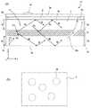
在折射率不同的两个光传播介质之间使光传播时,因为在界面存在光的透射和反射,所以使光以高效率从一方的光传播介质向另一方的光传播介质进行移动、且这一状态得以保持,这通常是困难的。作为从空气等的环境介质向透明板进行光的引入的技术,例如,可列举非专利文献1所示的现有的光栅耦合法。图32(a)和(b)是表示光栅耦合法的原理的说明图,表示在表面设有间距Λ的直线光栅的透光层20的剖面图和俯视图。如图32(a)所示,若对光栅以特定的入射角θ使波长λ的光23a入射,则能够使之与透光层20内传播的导波光23B耦合。When light is propagated between two light transmission media having different refractive indices, since there is transmission and reflection of light at the interface, the light is efficiently moved from one light transmission medium to the other light transmission medium, and This state is maintained, which is often difficult. As a technique for introducing light into a transparent plate from an ambient medium such as air, for example, the conventional grating coupling method disclosed in Non-Patent
【先行技术文献】【Prior technical literature】
【非专利文献】【Non-patent literature】
【非专利文献1】オ一ム社光集成电路,p94,p243西原浩等[Non-Patent Document 1] Oim Sheko Integrated Circuit, p94, p243 Hiroshi Nishihara, etc.
但是,根据非专利文献1所公开的方法,在透光层20中,只能引入满足所确立的条件的光,却无法引入偏离条件的光。However, according to the method disclosed in Non-Patent
发明内容Contents of the invention
本公开的实施方式,提供一种可以使光得以高效率地引入的取光板和棒。另外,本公开的实施方式,还提供具备它们的光接收装置和发光装置。Embodiments of the present disclosure provide a light-trapping plate and a rod that can efficiently introduce light. In addition, embodiments of the present disclosure also provide a light receiving device and a light emitting device including them.
本公开的取光板,具备如下:具有第一和第二主面的透光板;在所述透光板内的、且从所述第一和第二主面分别隔开了第一和第二距离以上的内部所配置的至少一个光耦合构造,所述至少一个光耦合构造含有第一透光层、第二透光层、和夹在其间的第三透光层,所述第一和第二透光层的折射率比所述透光板的折射率小,所述第三透光层的折射率比所述第一和第二透光层的折射率大,所述第三透光层具有与所述透光板的所述第一和第二主面平行的衍射光栅,所述取光板还具备:在所述透光板的所述第一和第二主面的至少一方经由间隙对置的透明盖板。The light-trapping sheet of the present disclosure includes the following: a light-transmitting plate having first and second main surfaces; and a first and second light-transmitting plate inside the light-transmitting plate and separated from the first and second main surfaces, respectively. At least one light-coupling structure configured inside the distance of more than two, the at least one light-coupling structure contains a first light-transmitting layer, a second light-transmitting layer, and a third light-transmitting layer sandwiched therebetween, the first and The refractive index of the second transparent layer is smaller than that of the transparent plate, the refractive index of the third transparent layer is larger than that of the first and second transparent layers, and the third transparent layer The optical layer has a diffraction grating parallel to the first and second main surfaces of the light-transmitting plate, and the light-trapping plate further includes: Transparent cover panels opposed via a gap.
本公开的取光棒具备如下:具有主面和圆或椭圆的截面的透光棒;在所述透光棒内的、且从所述主面隔开了第一距离以上的内部所配置的至少一个光耦合构造,并且,所述至少一个光耦合构造含有第一透光层、第二透光层、和夹在其间的第三透光层,所述第一和第二透光层的折射率比所述透光棒的折射率小,所述第三透光层的折射率比所述第一和第二透光层的折射率大,所述第三透光层具有与所述透光棒的中心轴平行的衍射光栅,所述取光棒还具备:在所述透光棒的所述主面经由间隙对置的透明盖板。The light-trapping rod of the present disclosure includes the following: a light-transmitting rod having a main surface and a circular or elliptical cross-section; At least one optical coupling structure, and the at least one optical coupling structure contains a first light-transmitting layer, a second light-transmitting layer, and a third light-transmitting layer sandwiched therebetween, the first and second light-transmitting layers The refractive index is smaller than that of the light-transmitting rod, the refractive index of the third light-transmitting layer is larger than that of the first and second light-transmitting layers, and the third light-transmitting layer has the same The central axis of the light-transmitting rod is parallel to the diffraction grating, and the light-trapping rod further includes: a transparent cover plate facing the main surface of the light-transmitting rod through a gap.
本公开的光接收装置具备如下:上述任一项所规定的取光板;在所述取光板的所述第一主面或所述第二主面所设置的凹凸构造或棱镜板;接收从所述凹凸构造或所述棱镜板出射的光的光电转换部。The light-receiving device of the present disclosure has the following: the light-trapping sheet specified in any one of the above; the concave-convex structure or the prism plate provided on the first main surface or the second main surface of the light-trapping sheet; The photoelectric conversion part of the concave-convex structure or the light emitted by the prism plate.
本公开的发光装置具备如下:上述任一项所规定的取光板或取光棒;在所述透光板或透光棒的主面邻接地配设的至少一个光源。The light-emitting device of the present disclosure includes the following: the light-trapping plate or the light-trapping rod specified in any one of the above; and at least one light source adjacent to the main surface of the light-transmitting plate or the light-transmitting rod.
根据本公开的实施方式,可以利用光的全反射,将光高效率地引入透光板或透光棒内。According to the embodiments of the present disclosure, light can be efficiently introduced into the light-transmitting plate or the light-transmitting rod by utilizing the total reflection of light.
附图说明Description of drawings
图1(a)是表示本公开的取光板的第一实施方式的模式化的剖面图,(b)是表示第一实施方式的第四区域的位置的俯视图。1( a ) is a schematic cross-sectional view showing the first embodiment of the light-trapping sheet of the present disclosure, and ( b ) is a plan view showing the position of the fourth region of the first embodiment.
图2(a)和(b)是表示第一实施方式的光耦合构造的模式化的剖面图和俯视图,(c)是表示入射到光耦合构造的端面的光的情况的剖面图,(d)是表示入射到抽取掉透光层3c的光耦合构造的光的情况的剖面图,(e)是表示光耦合构造的其他构成例的剖面图。2( a) and (b) are schematic cross-sectional views and plan views showing the optical coupling structure of the first embodiment, (c) is a cross-sectional view showing the state of light incident on the end face of the optical coupling structure, (d ) is a cross-sectional view showing how light is incident on the light-coupling structure with the light-transmitting
图3是表示用于第一实施方式的取光板的分析之构造的剖面图。3 is a cross-sectional view showing a structure used for analysis of the light-trapping sheet of the first embodiment.
图4是使用图3所示的构造进行的分析结果,(a)至(c)表示光的入射角与向板外的透射率的关系,(d)表示衍射光栅的凹槽深度与光向板外的光引出效率的关系。Fig. 4 is the analysis result using the structure shown in Fig. 3, (a) to (c) show the relationship between the incident angle of light and the transmittance to the outside of the plate, (d) shows the groove depth of the diffraction grating and the light direction The relationship between the light extraction efficiency outside the board.
图5(a)至(e)表示由图4(a)至(c)的箭头表示的位置的条件下的板截面的光强度分布图。5( a ) to ( e ) show light intensity distribution diagrams of the plate cross section under the conditions of the positions indicated by the arrows in FIGS. 4( a ) to ( c ).
图6是在图3所示的构造中,使第一透光层3a和第二透光层3b的折射率与透光板的折射率一致、使第三透光层3c的折射率为2.0时的分析结果,(a)至(c)表示入射角与向板外的透射率的关系,(d)表示衍射光栅的凹槽深度与光向板外的光引出效率的关系。Fig. 6 shows that in the structure shown in Fig. 3, the refractive index of the first light-transmitting
图7(a)至(e)是表示第一实施方式的取光板的制造步骤的模式化的剖面图。7( a ) to ( e ) are schematic cross-sectional views showing manufacturing steps of the light-trapping sheet of the first embodiment.
图8(a)和(b)是表示用于第一实施方式的取光板的制造之模具的表面图案的模式化的俯视图。8( a ) and ( b ) are schematic plan views showing a surface pattern of a mold used for manufacturing the light-trapping sheet of the first embodiment.
图9(a)和(b)是表示本公开的取光板的第二实施方式中使用的光耦合构造的模式化的剖面图和俯视图。9( a ) and ( b ) are schematic cross-sectional views and plan views showing an optical coupling structure used in a second embodiment of the light-trapping sheet of the present disclosure.
图10是表示用于第二实施方式的取光板的分析之构造的剖面图。10 is a cross-sectional view showing a structure used for analysis of a light-trapping sheet according to a second embodiment.
图11是使用图10所示的构造进行的分析结果,(a)至(c)表示入射角与向板外的透射率的关系,(d)表示衍射光栅的凹槽深度与光向板外的光引出效率的关系。Fig. 11 is an analysis result using the structure shown in Fig. 10, (a) to (c) show the relationship between the incident angle and the transmittance to the outside of the plate, and (d) shows the relationship between the groove depth of the diffraction grating and the light transmittance to the outside of the plate. The relationship between the light extraction efficiency.
图12是使用图3和图10所示的构造、且使光源的位置沿x轴的负的方向偏移5μm而进行的分析结果,(a)至(c)表示光朝向单一的光耦合构造的端面之入射角与向板外的透射率的关系。Fig. 12 is the analysis result using the structure shown in Fig. 3 and Fig. 10 and shifting the position of the light source by 5 μm in the negative direction of the x-axis, (a) to (c) represent the light-oriented single light coupling structure The relationship between the incident angle of the end face and the transmittance to the outside of the plate.
图13(a)至(e)是表示第二实施方式的取光板的制造步骤的模式化的剖面图。13( a ) to ( e ) are schematic cross-sectional views showing the manufacturing steps of the light-trapping sheet of the second embodiment.
图14(a)和(b)是表示本公开的取光板的第三实施方式中使用的光耦合构造的模式化的剖面图和俯视图。14( a ) and ( b ) are schematic cross-sectional views and plan views showing an optical coupling structure used in a third embodiment of the light-trapping sheet of the present disclosure.
图15是表示用于第三实施方式的取光板的分析之构造的剖面图。15 is a cross-sectional view showing a structure used for analysis of a light-trapping sheet according to a third embodiment.
图16是使用图15所示的构造进行的分析结果,(a)至(c)表示入射角与向板外的透射率的关系,(d)表示衍射光栅的凹槽深度与光向板外的光引出效率的关系。Fig. 16 is an analysis result using the structure shown in Fig. 15, (a) to (c) show the relationship between the incident angle and the transmittance to the outside of the plate, and (d) shows the relationship between the groove depth of the diffraction grating and the light transmittance to the outside of the plate. The relationship between the light extraction efficiency.
图17是使用图3和图15所示的构造、且使光源的位置沿x轴的负的方向偏移5μm而进行的分析结果,(a)至(c)表示光朝向单一的光耦合构造的端面之入射角与向板外的透射率的关系。Fig. 17 is the analysis result using the structure shown in Fig. 3 and Fig. 15 and shifting the position of the light source by 5 μm in the negative direction of the x-axis. The relationship between the incident angle of the end face and the transmittance to the outside of the plate.
图18(a)至(f)是表示第三实施方式的取光板的制造步骤的模式化的剖面图。18( a ) to ( f ) are schematic cross-sectional views showing the manufacturing steps of the light-trapping sheet of the third embodiment.
图19(a)和(b)是表示用于第三实施方式的取光板的制造之模具的表面图案的模式化的俯视图。19( a ) and ( b ) are schematic plan views showing a surface pattern of a mold used for manufacturing the light-trapping sheet of the third embodiment.
图20是表示本公开的光接收装置的实施方式的模式化的剖面图。20 is a schematic cross-sectional view showing an embodiment of the light receiving device of the present disclosure.
图21是表示本公开的光接收装置的其他的实施方式的模式化的剖面图。21 is a schematic cross-sectional view showing another embodiment of the light receiving device of the present disclosure.
图22是表示本公开的光接收装置的其他的实施方式的模式化的剖面图。22 is a schematic cross-sectional view showing another embodiment of the light receiving device of the present disclosure.
图23是表示本公开的光接收装置的其他的实施方式的模式化的剖面图。23 is a schematic cross-sectional view showing another embodiment of the light receiving device of the present disclosure.
图24是表示本公开的光接收装置的其他的实施方式的模式化的剖面图。24 is a schematic cross-sectional view showing another embodiment of the light receiving device of the present disclosure.
图25是表示本公开的采光板的实施方式的模式化的剖面图。Fig. 25 is a schematic cross-sectional view showing an embodiment of the lighting panel of the present disclosure.
图26是表示本公开的发光装置的实施方式的模式化的剖面图。Fig. 26 is a schematic cross-sectional view showing an embodiment of the light emitting device of the present disclosure.
图27(a)和(b)是表示本公开的取光棒的实施方式的与中心轴平行和垂直的模式的剖面图。27( a ) and ( b ) are cross-sectional views showing the modes parallel to and perpendicular to the central axis of an embodiment of the light-trapping rod of the present disclosure.
图28是表示图27所示的取光棒的制造步骤的模式化的图。FIG. 28 is a schematic view showing a manufacturing procedure of the light-trapping rod shown in FIG. 27 .
图29是表示本发明的发光装置的其他实施方式的模式化的剖面图。Fig. 29 is a schematic cross-sectional view showing another embodiment of the light-emitting device of the present invention.
图30是表示图29所示的发光装置的取光棒的截面的光的入射的情况的剖面图。30 is a cross-sectional view showing how light is incident on the cross-section of the light-trapping rod of the light-emitting device shown in FIG. 29 .
图31是表示本发明的发光装置的其他实施方式的模式化的剖面图。Fig. 31 is a schematic cross-sectional view showing another embodiment of the light-emitting device of the present invention.
图32(a)和(b)是用于通过光栅耦合法进行光的引入的直线光栅的剖面图和俯视图,(c)和(d)是表示光栅耦合法的原理的图。32( a ) and ( b ) are cross-sectional and plan views of a linear grating used to introduce light by the grating coupling method, and ( c ) and ( d ) are diagrams showing the principle of the grating coupling method.
图33(a)和(b)是表示本公开的取光板的又一其他实施方式的模式化的剖面图。33( a ) and ( b ) are schematic cross-sectional views showing yet another embodiment of the light-trapping sheet of the present disclosure.
具体实施方式Detailed ways
首先,说明本发明者关于前述现有技术的课题的考察。First, considerations of the present inventors on the problems of the aforementioned prior art will be described.
图32(c)表示入射到设于透光层20的光栅的光的矢量图。在图32(c)中,圆21、22以点O为中心,圆21的半径等于包围透光层20的环境介质1的折射率n0,圆22的半径等于导波光23B的等效折射率neff。等效折射率neff依存于透光层20的厚度,根据波导模式而取环境介质1的折射率n0至透光层20的折射率n1之间的特定的值。图32(d)表示光在透光层20以TE模式进行传播时的实效的厚度teff与等效折射率neff的关系。所谓实效的厚度,就是在没有光栅时透光层20的厚度本身,在有光栅时在透光层20的厚度上加上光栅的平均高度。在所激发的导波光中存在0级、1级、2级等的模式,如图32(d)所示,特性曲线各不相同。在图32(c)中,点P是从点O沿着入射角θ引出线、而与圆21交叉的点,点P’是点P到x轴的垂足,点Q、Q’是圆22与x轴的交点。朝向x轴正向的光的耦合条件,由P’Q的长度等于λ/Λ的整数倍表示;朝向负向的光的耦合条件由P’Q’的长度等于λ/Λ的整数倍表示。其中,λ是光的波长,Λ是光栅的间距。即,光的耦合条件由式(1)表示。FIG. 32( c ) shows a vector diagram of light incident on the grating provided in the light-transmitting
【算式1】【Equation 1】
在此,q是以整数表示的衍射级数。在由式(1)决定的θ以外的入射角下,光不会在透光层20内耦合。另外,即使是相同的入射角θ,如果波长不同,光仍然无法耦合。Here, q is a diffraction order represented by an integer. At incident angles other than θ determined by the formula (1), light is not coupled into the light-transmitting
还有,如图32(b)所示,以从光23a的入射方向移动了角度


另外导波光23B在光栅的区域传播期间,在与相对于入射光23a的反射光相同的方向上放射出光23b’。因此,在距光栅的端部20a远的位置入射,作为导波光23B即使能够在透光层20传播,也会在到达光栅的端部20a时有所衰减。因此,只有在靠近光栅的端部20a的位置入射的光23a不会受到因放射造成的衰减,能够作为导波光23B在透光层20内传播。就是说,为了使大部分的光耦合,即使增大光栅的面积,也不能使入射到光栅的光的全部作为导波光23B而进行传播。In addition, while the guided light 23B propagates in the area of the grating, the light 23b' is emitted in the same direction as the reflected light with respect to the
对于上述的现有技术,根据本公开的实施方式的取光板和取光棒,如后述,入射到透光板和透光棒的光,入射其内部所配置的光耦合构造,通过光耦合构造内的第三透光层的衍射光栅,被转换成沿着第三透光层的方向上传播的光,从光耦合构造的端面放射。光耦合构造处于与透光板表面或棒中心轴平行的位置关系,从光耦合构造放射的光在透光板的表面、透光棒的表面、和其他的光耦合构造的表面之间反复发生全反射,被封闭在透光板内或透光棒内。Regarding the above-mentioned prior art, according to the light-trapping plate and the light-trapping rod according to the embodiments of the present disclosure, as described later, the light incident on the light-transmitting plate and the light-transmitting rod enters the light-coupling structure configured inside it, and passes through the light-coupling structure. The diffraction grating of the third light-transmitting layer in the structure is converted into light propagating in a direction along the third light-transmitting layer, and radiated from the end face of the light-coupling structure. The light-coupling structure is in a positional relationship parallel to the surface of the light-transmitting plate or the center axis of the rod, and the light emitted from the light-coupling structure repeatedly occurs between the surface of the light-transmitting plate, the surface of the light-transmitting rod, and the surface of other light-coupling structures Total reflection, enclosed in a light-transmitting plate or a light-transmitting rod.
(第一实施方式)(first embodiment)
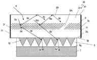
说明本公开的取光板的第一实施方式。图1(a)是取光板51的模式化的剖面图。取光板51具备:具有第一主面2p和第二主面2q的透光板2;和在透光板2内所配置的多个光耦合构造3。A first embodiment of the light-trapping sheet of the present disclosure will be described. FIG. 1( a ) is a schematic cross-sectional view of the light-trapping
透光板2由透射与用途相应的希望的波长的光的、或透射希望的波长域内的光的透明的材料构成。例如,由透过可视光(波长0.4μm以上、0.7μm以下)的材料的构成。透光板2的厚度例如为0.03mm~1mm左右。第一主面2p和第二主面2q的大小没有特别限制,具有与用途相应的面积。The light-transmitting
在该透光板2之上以夹隔垫片2d的方式粘接有盖板2e。因此,透光板2的第一主面2p的大部分与缓冲层2f相接。垫片2d由气凝胶这样的折射率比透光板低的材料构成。还有,盖板2e也可以形成在透光板2的第二主面2q,也可以形成在两面。盖板2e的厚度例如为0.1mm~1.0mm左右。A
如图1(a)所示,在透光板2内,光耦合构造3被配置在距第一主面2p和第二主面2q分别隔开第一距离d1和第二距离d2以上的内部。因此,在透光板2中,在与第一主面2p相接且厚度具有第一距离d1的第一区域2a、和与第二主面2q相接且厚度具有第二距离d2的第二区域2b中,未配设光耦合构造3,而在夹于第一区域2a和第二区域2b间的第三区域2c中配设有光耦合构造3。As shown in FIG. 1(a), in the light-transmitting
就光耦合构造3而言,在透光板2的第三区域2c中,被三维排列。优选光耦合构造3在与第一主面2p和第二主面2q平行的面被二维排列,并且,二维排列的多个光耦合构造3在透光板2的厚度方向上多层层叠。在此,所谓“平行”,不需要是数学上严格意义上的平行。本说明书中的“平行”的用语,包括相对于严格平行的方向在10度以下的范围内倾斜的情况。The
光耦合构造3在x、y轴方向(面内方向)和z轴方向(厚度方向)上以规定的密度配置。例如,就其密度而言,在x轴方向上每1mm为10~103个,在y轴方向上每1mm为10~103个,在z轴方向上每1mm为10~103个左右。为了使对透光板2的第一主面2p和第二主面2q全体所照射的光得以高效率地引入,透光板2的x轴方向、y轴方向和z轴方向的光耦合构造3的配置密度要分别独立而均匀。但是,根据用途和在透光板2的第一主面2p和第二主面2q所照射的光的分布,透光板2中的光耦合构造3的配置也可以不均匀,也可以具有规定的分布。The
图2(a)和(b)是沿着光耦合构造3的厚度方向的剖面图和与之正交的俯视图。光耦合构造3包含:第一透光层3a、第二透光层3b、和夹于其间的第三透光层3c。第一透光层3a、第二透光层3b和夹于其间的第三透光层3c,在与第一和第二主面(2p、2q)垂直的方向上并排配置。在此,所谓“垂直”,不需要是数学上严格意义上的垂直。本说明书中的“垂直”的用语,包括相对于严密地垂直的方向而在10度以下的范围内倾斜的情况。第三透光层3c包含配设在基准平面上的具有间距Λ的直线栅格的衍射光栅3d。衍射光栅3d的直线栅格,可以由在第三透光层3c与第一透光层3a或第二透光层3b的界面所设置的凹凸构成,也可以如图2(e)所示这样,设于第三透光层3c内部。另外,也可以不是由凹凸形成的栅格,而是由折射率差形成的栅格。光耦合构造3按照使第三透光层3c的衍射光栅3d与取光板51的第一主面2p和第二主面2q平行的方式配置在透光板2内。在此,所谓衍射光栅与第一主面2p和第二主面2q平行,意思是配设有栅格的基准平面与第一主面2p和第二主面2q平行。2( a ) and ( b ) are a sectional view along the thickness direction of the
在有的实施方式中,在与第一主面2p和第二主面2q平行的面上多个排列光耦合构造3时,至少以第一透光层3a和第二透光层3b彼此隔离的方式排列。即,在多个耦合构造3中含有在与第一和第二主面(2p、2q)平行的面中被二维地并排配置的、第一光耦合构造和第二光耦合构造时,第一光耦合构造具有的第一和/或第二透光层(3a、3b)、和第二光耦合构造具有的第一和/或第二透光层(3a、3b)彼此隔离。在此,所谓第一光耦合构造具有的第一和/或第二透光层(3a、3b)、和第二光耦合构造具有的第一和/或第二透光层(3a、3b)彼此隔离,包括以下任意一种情况。即,第一光耦合构造具有的第一透光层3a、和第二光耦合构造具有的第一透光层3a彼此隔离的情况;第一光耦合构造具有的第二透光层3b、和第二光耦合构造具有的第二透光层3b彼此隔离的情况;以及第一光耦合构造具有的第一和第二透光层(3a、3b)与第二光耦合构造具有的第一和第二透光层(3a、3b)分别彼此隔离的情况。第三透光层3c可以通过彼此隔离的方式排列,也可以通过彼此连续的方式排列。若从制造工艺容易这一点出发,则第三透光层3c能够以彼此连续的方式排列。就是说,第一光耦合构造具有的第三透光层、和第二光耦合构造具有的第三透光层能够彼此连续。In some embodiments, when a plurality of
使光耦合构造3沿透光板2的厚度方向多个排列时,以彼此隔离的方式排列。例如,在第一光耦合构造具有的第一透光层的上方、有第二光耦合构造具有的第二透光层时,第一光耦合构造具有的第一透光层、与第二光耦合构造具有的第二透光层以彼此隔离的方式排列。When a plurality of
第一透光层3a、第二透光层3b和第三透光层3c的厚度分别是a、b、t,第三透光层3c的直线衍射光栅的段差(深度)为d。第三透光层3c的表面与透光板2的第一主面2p、第二主面2q平行,第一透光层3a和第二透光层3b的、位于第三透光层3c相反侧的表面3p、3q,也与透光板2的第一主面2p、第二主面2q平行。The thicknesses of the first
如以下说明的,取光板51具备多个光耦合构造3,以使之能够将入射到取光板的不同波长的光引入,并且,在多个光耦合构造之中的至少两个中,衍射光栅3d的延伸方向可以互不相同。或者,在多个光耦合构造3之中至少两个中,衍射光栅3d的间距Λ可以互不相同。或者,也可以使以上情况加以组合。As explained below, the light-trapping
第一透光层3a和第二透光层3b的折射率比透光板2的折射率小,第三透光层3c的折射率比第一透光层3a和第二透光层3b的折射率大。以下,第一透光层3a和第二透光层3b是空气,折射率为1。另外,第三透光层3c由与透光板2相同的介质构成,折射率彼此相等。The refractive index of the first
光耦合构造3的第一透光层3a和第二透光层3b的表面3p、3q,例如,是以长度W和L为两条边的矩形,W和L为3μm以上、100μm以下。即,光耦合构造3的第一透光层3a和第二透光层3b的表面具有与3μm以上、100μm以下的直径的圆外切(外接)的大小。另外,光耦合构造3的厚度(a+t+d+b)为3μm以下。如图2(b)所示,在本实施方式中,光耦合构造3的表面(平面)具有矩形,但也可能具有其他的形状,例如,多角形、圆和椭圆形。The
就取光板51而言,在被环境介质包围下使用。例如,取光板51在空气中使用。这种情况下,环境介质的折射率为1。以下,将透光板2的折射率设为ns。来自环境介质的光4透过盖板2e和缓冲层2f,从透光板2的第一主面2p和第二主面2q入射到透光板2的内部。缓冲层2f由与环境介质相同的介质构成,其折射率为1。另外,垫片2d的折射率也大体上等于1。为了提高在盖板2e的两面和第一主面2p和第二主面2q入射的光4的透射率,也可以形成AR涂层和无反射纳米构造。在无反射纳米构造中,包含蝇眼结构等、使间距和高度为设计波长的1/3以下的微细的凹凸构造。设计波长是使取光板51发挥规定的机能来对各要素进行设计时所使用的光的波长。还有,在无反射纳米构造中,虽然菲涅耳反射减小,但全反射存在。The light-trapping
以下,将在透光板2的内部存在的光之中的、其传播方位与透光板2的法线(与第一主面2p和第二主面2q垂直的线)所形成的夹角θ(以下,称为传播角)满足sinθ<1/ns的光称为临界角内的光,将满足sinθ≥1/ns的光称为临界角外的光。在图1(a)中,透光板2的内部有临界角内的光5a时,其一部分经由光耦合构造3被转换成临界角外的光5b,该光在第一主面2p发生全反射,成为在板内部滞留的临界角外的光5c。另外,临界角内的光5a剩余的临界角内的光5a’之中的一部分经由别的光耦合构造3被转换成临界角外的光5b’,该光在第二主面2q发生全反射,成为在板内部滞留的临界角外的光5c’。如此临界角内的光5a的全部,在配置有光耦合构造3的第三区域2c内被转换成临界角外的光5b和5b’。Hereinafter, the angle formed by the propagation azimuth of the light existing inside the light-transmitting
另一方面,在透光板2中有临界角外的光6a时,其一部分在光耦合构造3的表面发生全反射而成为临界角外的光6b,该光在第一主面2p发生全反射,成为在板内部滞留的临界角外的光6c。另外,光6a的剩余的光的一部分成为透过设有光耦合构造3的第三区域2c的临界角外的光6b’,该光在第二主面2q发生全反射,成为在透光板2内部滞留的临界角外的光6c’。另外虽然在图中未显示,但一边在不同的光耦合构造3之间和第一主面2p、第二主面2q之间发生全反射,一边在板内部滞留的临界角外的光,即,在第一区域2a、第二区域2b或第三区域2c中滞留而传播的光也存在。这种情况下,在第一区域2a和第二区域2b传播的光的分布产生偏移之虞存在。透光板2的光的分布的偏移成为问题时,如图1(a)所示,在透光板2内的第三区域2c中,能够设置一个以上没有配设光耦合构造3的第四区域2h。就是说,光耦合构造3只在除去第四区域2h的第三区域2c内配置。在透光板2中,第四区域2h连接第一区域2a和第二区域2b。第四区域2h从第一区域2a向第二区域2b或沿相反方向延伸,贯通第四区域2h的任意的直线的方位,沿着比由透光板的折射率和透光板的周围的环境介质的折射率所规定的临界角大的角度。即,如果环境介质的折射率为1,透光板2的折射率设为ne,则贯通第四区域2h的任意的直线的延伸的方向2hx与透光板2的法线的所形成角度θ’满足sinθ’≥1/ns。在此,所谓直线贯通第四区域2h,是指直线贯通第四区域2h的与第一区域2a相接的面和第四区域2h的第二区域2b。On the other hand, when there is light 6a beyond the critical angle in the light-transmitting
图1(b)是取光板51的俯视图,表示第四区域2h的配置。如图1(b)所示,第四区域2h,优选在透光板2内设有多个。第四区域2h,因为以比临界角大的角度从第一区域2a向第二区域2b或相反的方向伸长,所以只有在透光板2的第一区域2a和第二区域2b传播的光之中的、临界角外的光,能够透过第四区域2h,并从第一区域2a向第二区域2b透过或反方向透过。因此,能够防止取光板51内的光分布的偏移。FIG. 1( b ) is a top view of the light-trapping
如图2(a)所示,临界角内的光5a,透过第二透光层3b的表面3q,其一部分在衍射光栅3d的作用下被转换成在第三透光层3c内传播的导波光5B。其余作为透射光和衍射光,主要成为临界角内的光5a’而透过光耦合构造3、或作为反射光而成为临界角内的光5r,穿过光耦合构造3。向第二透光层3b入射时,虽然也有在表面3q反射的临界角外的光6b,但如果在表面3q、3p形成无反射纳米构造,则能够使大部分的光透过。As shown in Figure 2 (a), the light 5a in the critical angle passes through the
向导波光5B的耦合,与现有的光栅耦合法的原理相同。就导波光5B而言,在到达第三透光层3c的端面3S以前,其一部分沿着与临界角内的光5r相同的方向被放射,成为临界角内的光5r’;剩余的作为导波从第三透光层3c的端面3S被放射,成为临界角外的光5c。另一方面,临界角外的光6a,在第二透光层3b的表面3q发生全反射,其全部成为临界角外的光6b。如此,入射到光耦合构造3的表面(第一透光层3a的表面3p和第二透光层3b的表面3q)的临界角外的光作为临界角外的光直接被反射,临界角内的光其一部分被转换成临界角外的光。The principle of the coupling of the
还有,若第三透光层3c的衍射光栅3d的长度过长,则导波光5B在到达其端面3S之前便全部被放射。另外若过短,则向导波光5B的耦合效率不充分。导波光5B的易放射度由放射损耗系数α表示,在传播距离L下,导波光5B的强度变成exp(-2αL)倍。假如α的值设为10(1/mm),则在10μm的传播下达到0.8倍的光强度。放射损耗系数α与衍射光栅3d的深度d有关,在d≤dc的范围内单调递增,在d>dc的范围内饱和。若设光的波长为λ,导波光5B的等效折射率为neff,透光层3c的折射率为n1,衍射光栅3d的占空比(デユ一テイ)(凸部的宽度对于间距的比)为0.5,则dc由以下的式(2)给出。Also, if the length of the
【算式2】
例如,若λ=0.55μm,neff=1.25,n1=1.5,则dc=0.107μm。在单调递增区域,放射损耗系数α与d的平方成正比。因此,衍射光栅3d的长度,即第三透光层3c的长度(尺寸W和L)由放射损耗系数α决定,依存于衍射光栅3d的深度d。假如,调整深度d而将α的值设定在2~100(1/mm)的范围,使衰减比为0.5,则W和L为3μm至170μm左右。因此,如上述,如果W和L为3μm以上、100μm以下,则通过深度d的调整能够抑制放射损耗,得到高耦合效率。For example, if λ=0.55 μm, neff =1.25, n1 =1.5, then dc =0.107 μm. In the monotonically increasing region, the radiation loss coefficient α is proportional to the square of d. Therefore, the length of the
在使导波光5B的等效折射率neff为1.25时,根据式(1),对应间距Λ、入射角θ,哪种可视光的波长(λ=0.4~0.7μm)的光进行耦合被示出在(表1)中。虚线的区间为耦合的范围。例如,间距0.4μm的情况下,在θ=-14度下,波长0.4μm的光耦合,在θ=30度下,波长0.7μm的光耦合,从θ=-14度至θ=30度为可视光的耦合范围。When the equivalent refractive index neff of the
【表1】【Table 1】

入射角θ的极性与光的耦合方向相关。因此,若无视光的耦合方向而仅仅注目于有无耦合,如果入射角的范围覆盖从0到90度、或从-90到0度的任意一个范围,则全部的入射角度所对应的耦合可进行。因此,由表1可知,为了对于全部的可视光波长、全部的入射角度而使光耦合,能够组合使用具有0.18μm至0.56μm(0度至90度),或0.30μm至2.80μm(-90度至0度)的间距Λ的衍射光栅3d的光耦合构造3。若考虑等效折射率的变化和形成导波层和衍射光栅时所能够产生的制造误差,则衍射光栅3d的间距大概为0.1μm以上、3μm以下即可。The polarity of the incident angle θ is related to the coupling direction of the light. Therefore, if we ignore the coupling direction of light and only focus on the presence or absence of coupling, if the range of incident angle covers any range from 0 to 90 degrees, or from -90 to 0 degrees, then the coupling corresponding to all incident angles can be conduct. Therefore, it can be seen from Table 1 that in order to couple light for all wavelengths of visible light and all incident angles, it is possible to use in
另外,如图2(b)所示,例如,在与衍射光栅3d延伸方向垂直的方向所入射的临界角内的光5a所对应的衍射光栅3d的间距为Λ,但以方位角φ入射的光5aa所对应的衍射光栅3d的实效的间距为
接着,研究与光耦合构造3的表面3p、3q垂直的端面3r、3s(沿着透光层3b的法线方向的面)中的光。如图2(c)所示,就光耦合构造3的端面3r所入射的光而言,考虑有如下情况:在端面3r反射的情况;在端面3r发生衍射的情况;透过端面3r而发生折射的情况;经过端面3r而在第三透光层3c导波的情况。例如,在第一透光层3a和第二透光层3b的端面入射且透过的临界角外的光6a,发生折射,且成为临界角内的光6a’。另外,在第三透光层3c的端面入射并透过的光6A的一部分,被转换成在第三透光层3c内传播的导波光6B。Next, the light in the
作为参考,图2(d)表示从光耦合构造3抽取掉第三透光层3c、且在所抽取后的空间用与第一透光层3a和第二透光层3b相同的空气填充时的光路。临界角内的光5a在光耦合构造3的表面3q入射时,如果其入射位置接近端面3s,则折射的结果是,在端面3s作为临界角外的光5a’出射。另外,临界角内的光5a在光耦合构造3的端面3r入射时,在端面3r发生全反射。临界角外的光6a在光耦合构造3的端面3r入射时,在此入射位置不聚集,折射的结果,从表面3p作为临界角内的光6a’出射。另外,临界角外的光6a入射到光耦合构造3的表面3q时,在表面3q发生全反射。For reference, Fig. 2(d) shows that the third light-transmitting
如此,光耦合构造3的端面3r、3s所入射的光的情况,其举动复杂,即使临界角外的光入射端面,也未必作为临界角外的光出射。但是,如果使表面的大小(W、L)比端面的大小(a+t+d+b)大得多(例如4倍以上),则端面的影响十分小,表面3p、3q的光的透射或反射能够视为光耦合构造3整体的光的透射和反射的举动。具体来说,第一透光层3a的表面3p和第二透光层3b的表面3q的大小,如果是光耦合构造3的厚度的4倍以上,则能够足以无视光耦合构造3的端面3r、3s中光的影响。因此,如果光耦合构造3将临界角外的光保持作为临界角外的光,另一方面,发挥将临界角内的光不可逆地转换为临界角外的光的机能,充分设定光耦合构造3的密度,则能够将入射到取光板51的全部的光转换成临界角外的光(即在板内所封闭的光)。In this way, the behavior of light incident on the end faces 3r and 3s of the
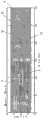
图3表示用于确认取光板51中的光封闭效果的分析所使用的取光板的截面构造。分析中,使用含有一个光耦合构造的取光板。如图3所示,在从透光板2的第二主面2q距1.7μm的位置平行地设定宽5μm的光源S(由虚线表示),在其上方空出0.5μm的距离而平行配置宽6μm的第二透光层3b,在其上配置相同宽度的第三透光层3c和第一透光层3a。透光板2的第一主面2p处于从第一透光层3a的表面距2.5μm的位置。从光源S,在相对于第二主面2q的法线而构成θ的角的方位,出射相对于纸面成45度的角度的偏振光的平面波,按照使入射光的中心透过第二透光层3b的表面的中心的方式,根据角θ而使第一透光层3a、第二透光层3b和第三透光层3c的位置横向移动。另外,使第一透光层3a的厚度a为0.3μm,第二透光层3b的厚度c为0.3μm,第三透光层3c的厚度t为0.4μm,衍射光栅的深度d为0.18μm,衍射光栅的间距Λ为0.36μm。使透光板2和第三透光层3c的折射率为1.5,环境介质、第一透光层3a和第二透光层3b的折射率为1.0。FIG. 3 shows a cross-sectional structure of a light-trapping sheet used in an analysis for confirming the light-trapping effect in the light-trapping
图4(a)至(c)是表示在图3所示的构造的取光板中,从光源S向光耦合构造3入射的光的入射角θ、与向取光板外出射的光的透射率的关系的分析结果。用于分析的构造如上述。分析中使用二维的时域有限差分法(FDTD)。因此,是图3所示的截面在纸面垂直方向上无限延续的构造的分析结果。就透射率而言,其是稳定时的计测,以通过分析区域最下面(z=0μm)和最上面的坡印廷矢量(Poynting Vector)的积分值、对通过包围光源的闭曲面的坡印廷矢量的积分值之比定义。虽然有一部分超过100%的计算结果,但这是由于光源的坡印廷矢量的计测有一些误差。图4(a)表示光源的波长λ为0.45μm时的计算结果,图4(b)表示波长λ为0.55μm时的计算结果,图4(c)表示波长λ为0.65μm时的计算结果。分别将衍射光栅的深度d作为参数、并且在没有光耦合构造3的条件(只有透光板2和光源S的结构)下的结果也加以绘制。4(a) to (c) show the incident angle θ of the light incident from the light source S to the
将有光耦合构造3但衍射光栅的深度d=0时的结果与没有光耦合构造时的结果(Nothing)比较,则前者与后者相比,在临界角(41.8度)以内的范围,透射率变小,在此以上的角度时均大体变成零。之所以在临界角以内前者的透射率变小,如参照图2(d)而说明的,是由于入射到第二透光层3b的表面3q的光发生折射,其一部分作为临界角外的光从端面3s出射。但是,在前者的情况下,相同地如参照图2(c)、(d)而说明的,从光耦合构造3的端面3r入射的临界角外的光,在该面发生折射后,又在第一透光层3a的表面3p折射,在透光板2内变成临界角内的光。因此,在d=0时的构造中,有向临界角外的光的转换,另一方面,也有向临界角内的光的转换,可以说整体上封闭光的效果小。Comparing the result when there is
另一方面,若将光栅的深度d=0.18μm时的结果与d=0时的结果进行比较,则前者的透射率与后者的大体上接近,但在箭头a、b、c、d、e的位置,透射率下降。图4(d)中将图4(a)、(b)、(c)的曲线就入射角θ进行积分后的值的标准值(除以90的值)、在以衍射光栅的深度d作为参数下加以表示。因为分析模型为二维,所以该积分值等于光封闭板内的光被引出到板外的效率。任何波长下,随着d的增大(至少在d=0,d=0.18的比较中),引出效率均降低。这呈现出由单一的光耦合构造带来的光封闭的效果。如果这一效果能够累积,使光耦合构造的数量增加,则最终能够封闭全部的光。还有,虽然本分析是二维的模型,但在实际的模型(三维模型)中,因为相对于图2(a)的俯视图所示的任意的方位角φ而满足作为耦合条件的式(1)的入射光必然存在,所以图4所示的透射率的曲线并非在箭头a、b、c、d、e等局部性的范围、而在全部的入射角θ的范围下降,光耦合构造带来的光封闭的效果变得更大。On the other hand, if the grating depth d=0.18μm is compared with the result when d=0, the transmittance of the former is roughly close to that of the latter, but the arrows a, b, c, d, At the position of e, the transmittance decreases. In Fig. 4(d), the standard value (the value divided by 90) of the value after integrating the curves of Fig. 4(a), (b), and (c) with respect to the angle of incidence θ is taken as the depth d of the diffraction grating indicated below the parameters. Since the analytical model is two-dimensional, this integral value is equal to the efficiency with which the light inside the light-tight panel is extracted to the outside of the panel. At any wavelength, as d increases (at least in the comparison between d=0 and d=0.18), the extraction efficiency decreases. This exhibits the effect of light confinement brought about by a single light coupling structure. If this effect is cumulative, increasing the number of light-coupling structures will eventually trap all the light. In addition, although this analysis is a two-dimensional model, in the actual model (three-dimensional model), since it satisfies the equation (1 ) incident light must exist, so the transmittance curve shown in Figure 4 is not in the local range of arrows a, b, c, d, e, etc., but falls in the range of all incident angles θ, the optical coupling structure belt The effect of coming light occlusion becomes even greater.
图5表示在图4的箭头a、b、c、d、e所示的条件下、取光板内的光强度分布图。具体来说,图5(a)表示波长λ=0.45μm,θ=5度的结果,图5(b)表示波长λ=0.55μm,θ=0度的结果,图5(c)表示波长λ=0.55μm,θ=10度的结果,图5(d)的波长λ=0.65μm,θ=10度的结果,图5(e)表示波长λ=0.65μm,θ=20度的结果。FIG. 5 shows the light intensity distribution diagram in the light-trapping panel under the conditions shown by the arrows a, b, c, d, and e in FIG. 4 . Specifically, Figure 5(a) shows the results for wavelength λ=0.45μm, θ=5 degrees, Figure 5(b) shows the results for wavelength λ=0.55μm, θ=0 degrees, and Figure 5(c) shows the results for wavelength λ =0.55 μm, the result of θ=10 degrees, the wavelength λ=0.65 μm of Fig. 5 (d), the result of θ=10 degrees, and Fig. 5 (e) shows the result of wavelength λ=0.65 μm, θ=20 degrees.
在图5(a)、(b)所示的条件和入射角的情况下,因为第三透光层3c的折射率比包围它的第一透光层3a和第二透光层3b的折射率高,所以第三透光层3c作为导波层发挥机能,入射光在衍射光栅的作用下,与在第三透光层3c内传播的导波光耦合,该光从第三透光层3c的端面3r、3s放射到透光板2内。该放射光是临界角外的光,在透光板2的第一主面2p和第二主面2q发生全反射,被封闭在透光板2内。图5(c)、(d)、(e)所示的条件和入射角的情况下,入射光也在衍射光栅的作用下与在第三透光层3c内传播的导波光耦合,该光从第三透光层3c的端面3r被放射到板内。该放射光是临界角外的光,在透光板2的第一主面2p和第二主面2q发生全反射,被封闭在透光板2内。还有,在图5(a)、(c)、(e)中,放射光被分为两股,所耦合的光在导波层截面的上下是相位反转的一级模式的导波光。另一方面,在图5(b)、(d)中,放射光处于聚合的状态,耦合的光为0级模式的导波光。Under the conditions and incident angles shown in Fig. 5(a), (b), because the refractive index of the third light-transmitting
图6表示:在图3所示的构造中使第一透光层3a和第二透光层3b的折射率与透光板2的折射率一致、且将第三透光层3c的折射率变更成2.0时的分析结果。其他条件均与能够得到图4所示的分析结果时的条件相同。图6(a)表示光源的波长λ=0.45μm时的结果,图6(b)表示波长λ=0.55μm时的结果,图6(c)表示波长λ=0.65μm时的结果。若将光栅的深度d=0.18μm时的结果与d=0时的结果比较,则前者的透射率与后者的相比,在箭头a、b、c、d、e、f的位置下降。这基于参照图4说明的相同理由。但是在临界角以上的区域,相比后者处于零邻域,前者大幅上升。这是因为,临界角以上的入射角的光由光耦合构造3的衍射光栅衍射,其一部分在板内被转换成临界角内的光。图6(d)中将图6(a)、(b)、(c)的曲线就入射角θ进行积分后的值的标准值(除以90的值)、在以凹槽深度d作为参数下加以表示。在几个条件下,随着d的增大,引出效率反而增大,得不到光封闭的效果。这表示在临界角以上的区域的特性抵消了箭头a、b、c、d、e、f的位置的效果。FIG. 6 shows: in the structure shown in FIG. 3, the refractive index of the first light-transmitting
若比较图4和图6所示的分析结果,则在图4中,在临界角以上,能够使透射率达到零。将光栅的深度d=0.18μm时的结果与d=0时的结果比较,在临界角以上的区域也没有差异,均大体为零。这是由于,因为使第一透光层3a和第二透光层3b的折射率比透光板2的折射率小,所以在第二透光层3b和透光板2的界面、即表面3q发生全反射,入射角大的光不能入射到光耦合构造3内的衍射光栅,没有由衍射光栅形成的衍射光发生。如此可知,作为光耦合构造3,为了第三透光层3c成为导光层,使其折射率比第一透光层3a和第二透光层3b的折射率大,为了临界角外的光不入射第三透光层3c,使第一透光层3a和第二透光层3b的折射率比透光板2的折射率小即可。另外可知,为了使透光板2和光耦合构造之间的全反射所对应的临界角减小,优选第一透光层3a和第二透光层3b的折射率与透光板的折射率的差要大,例如,第一透光层3a和第二透光层3b的折射率能够为1。Comparing the analysis results shown in FIG. 4 and FIG. 6 , in FIG. 4 , the transmittance can be made zero at the critical angle or more. Comparing the results when the depth of the grating d=0.18 μm and the result when d=0, there is no difference in the region above the critical angle, and both are substantially zero. This is because, because the refractive index of the first light-transmitting
如此根据本实施方式的取光板,在透光板的第一主面和第二主面以各种角度入射的光,成为临界角内的光而入射到在透光板的内部所配置的光耦合构造,经由光耦合构造内的衍射光栅,其一部分被转换成在第三透光层内传播的导波光,从光耦合构造的端面被放射,成为临界角外的光。根据光耦合构造,其衍射光栅的间距不同、或衍射光栅的方位不同,因此该转换可跨越全部的方位、宽阔的波长范围,例如可跨越可视光全域进行。另外,因为衍射光栅的长度短,所以能够减少导波光的放射损耗。因此,在透光板内存在的临界角内的光,通过多个光耦合构造而全部被转换成临界角外的光。因为光耦合构造的第一和第二透过层的折射率比透光板的折射率小,所以临界角外的光在光耦合构造的表面发生全反射,该光在其他的光耦合构造的表面和透光板的表面之间反复发生全反射,被封闭在透光板内。如此,光耦合构造将临界角内的光不可逆地转换成临界角外的光,另一方面,又将临界角外的光保持在临界角外的状态。因此,如果充分设定光耦合构造的密度,则能够将入射到取光板的全部的光转换成临界角外的光,即转换成封闭在板内的光。Thus, according to the light-trapping sheet of this embodiment, the light incident on the first main surface and the second main surface of the light-transmitting sheet at various angles becomes light within the critical angle and enters the light arranged inside the light-transmitting sheet. In the coupling structure, part of it is converted into guided light propagating in the third light-transmitting layer via the diffraction grating in the optical coupling structure, and is radiated from the end face of the optical coupling structure as light outside the critical angle. Depending on the optical coupling structure, the pitch of the diffraction grating is different, or the azimuth of the diffraction grating is different, so the conversion can be performed across all azimuths and a wide wavelength range, for example, across the entire range of visible light. In addition, since the length of the diffraction grating is short, radiation loss of guided light can be reduced. Therefore, all the light within the critical angle existing in the light-transmitting plate is converted into light outside the critical angle by the plurality of optical coupling structures. Because the refractive index of the first and second transmission layers of the light-coupling structure is smaller than that of the light-transmitting plate, the light outside the critical angle will be totally reflected on the surface of the light-coupling structure, and the light will be reflected on the surface of other light-coupling structures. Total reflection occurs repeatedly between the surface and the surface of the light-transmitting plate, and is enclosed in the light-transmitting plate. In this way, the light coupling structure irreversibly converts light within the critical angle into light outside the critical angle, and on the other hand, keeps the light outside the critical angle in a state outside the critical angle. Therefore, if the density of the light-coupling structure is set sufficiently, all the light incident on the light-trapping panel can be converted into light outside the critical angle, that is, into light enclosed in the panel.
还有,在图1(a)中,透光板2的第一主面2p经由缓冲层2f而被盖板2e覆盖。因此,水滴等的异物2g附着在盖板2e的表面,与第一主面2p接触得以防止。如果异物2g与第一主面2p接触,则在此接触面,全反射的关系破坏,在透光板2内所封闭的临界角外的光经由异物2g而泄漏到外部。垫片2d也与第一主面2p相接,但其折射率与环境介质的折射率几乎不变,因此在此接触面全反射的关系得到维持,临界角外的光不会经由垫片2d泄漏到外部。另外,透光板的表面积小时,也可以不夹隔垫片2d而在盖板2e与第一主面2p之间形成缓冲层2f。In addition, in FIG.1(a), the 1st
图33(a)和(b)是表示盖板2e的配置例的剖面图。在图33(a)的例子中,其构成为,在透光板2的第一主面2p和第二主面2q的两方经由“间隙”使盖板2e对置地构成。在该例中,第一主面2p和第二主面2q的全体由盖板2e覆盖。在图33(b)的例子中,透光板2的第一主面2p的一部分没有与盖板2e对置。另外,在该例中,垫片2d设于第二主面2q的端部以外的位置。还有,上述的“间隙”,也可以由折射率充分小的流体或固体填埋。Fig. 33(a) and (b) are cross-sectional views showing an arrangement example of the
取光板51,例如,能够通过以下的方法制造。图7(a)至(e)是表示取光板51的制造步骤的模式化的剖面结构图,图8(a)、(b)是表示用于制成板的模具表面的图案模式化的俯视图。The light-trapping
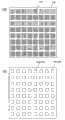
在图8(a)、(b)中,在模具25a、25b的表面,例如,相同尺寸的矩形微小构造25A、25B被二维排列。模具25a的微小构造25A的配置与模具25b的微小构造25B的配置等同。微小构造25A、25B在本实施方式中是突起。微小构造25A的高度相当于图2(a)的尺寸b,微小构造25B的高度相当于尺寸a。微小构造25B的表面是平面,但在微小构造25A的表面之上,形成有高度d、间距Λ的直线衍射光栅,衍射光栅的方位(凹部或凸部的延伸方向)在每个微小构造25A有所不同。在图8中,使0度、45度、90度、135度的按45度刻度的方位的光栅规则地排列,但实际上,能够以30度和15度刻度等更小的刻度幅度的方位而使光栅等频度地排列。In Fig. 8(a) and (b), on the surfaces of
如图7(a)所示,以在模具25b的表面薄薄地涂布分离剂的状态铺设透明的树脂板24,在该板上配置模具25a,在使彼此的微小构造25B与微小构造25A的位置对齐状态下,对夹在模具25b和模具25b中的树脂板24进行挤压。As shown in FIG. 7(a), a
如图7(b)所示,抬起模具25a,将树脂板24从模具25b上剥落,如图7(c)所示,压在表面薄薄地涂布有粘接剂的树脂板24a上,将树脂板24和树脂板24a粘接。如图7(d)所示,将粘接剂薄薄地涂布在树脂板24a的底面,将其在无视校准下压在通过同样的方法形成的树脂板24’、24’a之上,而将其粘接。As shown in Figure 7 (b), the
如图7(e)所示,以固定树脂板24’a的状态,抬起模具25a,从模具25a上剥落树脂板24、24a、24’、24’a的全体。As shown in Fig. 7(e), with the state of fixing the resin plate 24'a, the
之后,将树脂板24、24a、24’、24’a置换成图7(d)的树脂板24’、24’a,重复这些步骤,制作图1(a)所示的透光板2的第三区域2c。在透光板2的第三区域2c的表面和背面,粘接构成透光板2的第一区域2a和第二区域2b的树脂板,由此图1(a)所示的取光板51完成。在本实施方式中,树脂板的粘接中使用的是粘接剂,但也可以不使用粘接剂,而是通过对树脂板的表面加热,而使树脂板之间熔接。另外,也可以在树脂板24a和构成第一区域2a和第二区域2b的树脂板的表面预先形成无反射纳米构造。Afterwards, the
(第二实施方式)(second embodiment)
说明本公开的取光板的第二实施方式。本实施方式的取光板52,光耦合构造的端面的构造与第一实施方式的光耦合构造不同。因此,以下,以本实施方式的光耦合构造为中心进行说明。A second embodiment of the light-trapping sheet of the present disclosure will be described. The light-trapping
图9(a)和(b)模式化地表示沿着取光板52的厚度方向的光耦合构造3’的截面构造和平面构造。如图9(a)和(b)所示,在光耦合构造3’中,在端面3r、3s设有深度e的凹部3t。凹部3t的截面,随着朝向内部而宽度变窄。因此,在光耦合构造3’中,第一透光层3a和第二透光层3b的厚度,随着从光耦合构造3’的中心向外缘侧而变小。表面3p、3q与第一实施方式同样是平坦的。9 (a) and (b) schematically show the cross-sectional and planar structures of the light coupling structure 3' along the thickness direction of the light-trapping
图10表示为了确认具备光耦合构造3’的取光板52的光封闭的效果而用于分析的取光板的截面构造。光耦合构造和光源,设置在与用于第一实施方式的分析的构造(图3)对应的要素完全相同的位置上。Fig. 10 shows a cross-sectional structure of a light-trapping sheet used for analysis to confirm the light confinement effect of the light-trapping
图11(a)至(c)是表示在图10所示的构造的取光板中,从光源S向光耦合构造3’入射的光的入射角θ、与向取光板外出射的光的透射率的关系的分析结果。分析中使用与第一实施方式相同的方法。图11(a)表示光源的波长λ=0.45μm时的结果,图11(b)表示波长λ=0.55μm时的结果,图11(c)表示波长λ=0.65μm时的结果。其中,分别将衍射光栅的深度d作为参数、并且在没有光耦合构造的条件(只有透光板2和光源S的结构)下的结果也加以绘制。Fig. 11 (a) to (c) show that in the light-trapping sheet of the structure shown in Fig. 10, the incident angle θ of the light incident from the light source S to the light coupling structure 3', and the transmission of the light emitted to the outside of the light-trapping sheet The results of the analysis of the rate relationship. The same method as that of the first embodiment was used for the analysis. Figure 11(a) shows the result when the wavelength of the light source λ=0.45 μm, Figure 11(b) shows the result when the wavelength λ=0.55 μm, and Figure 11(c) shows the result when the wavelength λ=0.65 μm. Among them, the depth d of the diffraction grating is used as a parameter, and the results under the condition of no optical coupling structure (the structure of only the light-transmitting
将有光耦合构造3’但衍射光栅的深度d=0时的结果与没有光耦合构造时的结果(Nothing)比较,则前者与后者相比,在临界角(41.8度)以内的范围变小,在其以上的角度下两者均为零。之所以在临界角以内前者变小,如参照图2(d)说明的,是由于入射到第二透光层3b的表面3q的光发生折射,其一部分作为临界角外的光从右侧面(第三透光层3c的右侧面)出射。Comparing the result when there is an optical coupling structure 3' but the depth d=0 of the diffraction grating with the result (Nothing) when there is no optical coupling structure, the range within the critical angle (41.8 degrees) becomes smaller in the former than in the latter. Small, both are zero at angles above it. The reason why the former becomes smaller within the critical angle is that, as explained with reference to FIG. (the right side of the third light-transmitting
另一方面,若将光栅的深度d=0.18μm时的结果与d=0时的结果比较,则前者的透射率与后者的大体上接近,但在箭头a、b、c、d、e的位置,透射率下降。这些位置相当于光与导波光耦合的条件。图11(d)中将图11(a)、(b)、(c)的曲线就入射角θ进行积分后的值的标准值(除以90的值)、在以凹槽深度d作为参数下加以表示。因为分析模型是二维的,所以该积分值等于板内的光引出到板外的效率。无论哪种波长,伴随d的增大(至少在d=0、d=0.18的比较中),引出效率均降低。这表示由单一的光耦合构造带来的光封闭的效果,与第一实施方式的分析结果相同。如果这一效果能够累积,使光耦合构造的数量增加,则能够封闭全部的光。还有,虽然本分析是二维的模型,但在现实的三维模型中,因为相对于图2(a)的俯视图所示的任意的方位角
图12是表示第二实施方式中的、基于光向单一的光耦合构造的端面的入射之入射角θ和向取光板外的透射率的关系的分析结果。在分析条件中采用的是,仅将图10和图3中光源S的位置向x轴的负侧移动5μm的。图12(a)是光源的波长λ=0.45μm的情况,图12(b)是波长λ=0.55μm的情况,图12(c)是波长λ=0.65μm的情况,分别将本实施例的模型与第一实施方式的模型进行比较、并且在没有光耦合构造的条件(只有透光板2和光源S的结构)下的结果也加以绘制。12 is an analysis result showing the relationship between the incident angle θ of light incident on the end surface of a single optical coupling structure and the transmittance to the outside of the light-trapping plate in the second embodiment. As the analysis conditions, only the position of the light source S in FIG. 10 and FIG. 3 is moved to the negative side of the x-axis by 5 μm. Fig. 12 (a) is the situation of the wavelength λ=0.45 μm of the light source, Fig. 12 (b) is the situation of the wavelength λ=0.55 μm, and Fig. 12 (c) is the situation of the wavelength λ=0.65 μm. The model is compared with that of the first embodiment, and the results in the condition of no light-coupling configuration (a configuration with only the light-transmitting
若将第二实施方式的模型的结果与没有光耦合构造时的结果(Nothing)比较,则两方均是在临界角内(41.8度以下)大体一致,但在临界角外(41.8度以上)的范围,后者大体上为零,相对于此,前者从零大幅上升。前者之所以在临界角外上升,如参照图2(c)、(d)说明的,是由于入射到光耦合构造的第一透光层3a和第二透光层3b的端面的光在折射之后,成为临界角内的光而从第一主面2p出射。相对于此,第二实施方式的模型的分析结果是,临界角外的范围的上升得到部分地抑制。这是由于,在第二实施方式的端面,没有第一透光层3a和第二透光层3b占据的区域,端面的折射得到一定程度的抑制。因此,第二实施方式是能够在第一实施方式以上无视端面的影响(临界角外的光被转换成临界角内的光的现象)的结构,可以说是封闭光的效果更强的结构。还有,在图12中将光源的长度设定为5μm。若增长其长度,则从光耦合构造的端面偏离,直接入射到第一主面2p而发生全反射、或在光耦合构造的表面3q发生全反射的成分的比率增加,因此临界角外的上升缓和。假如使光源的长度达到4倍的20μm,使光耦合构造为21μm左右,则在维持其他的特性的同时,端面入射的特性在临界角外的上升降低至1/4左右。Comparing the results of the model of the second embodiment with the results without the optical coupling structure (Nothing), both are roughly consistent within the critical angle (below 41.8 degrees), but outside the critical angle (above 41.8 degrees). The range of the latter is roughly zero, while the former rises substantially from zero. The reason why the former rises outside the critical angle, as explained with reference to FIG. Thereafter, the light within the critical angle is emitted from the first
图13是表示本实施方式的取光板52的制作步骤的一例的模式化的截面。在模具25a、25b的微小构造25A、25B的外缘部设置倾斜25A’、25B’,如果使用与第一实施方式同样的步骤,则能够制造取光板52。如果除去模具25a、25b的形状不同这一点,则能够与第一实施方式的取光板51同样地制造本实施方式的取光板52,因此省略具体的制造步骤的说明。FIG. 13 is a schematic cross-section showing an example of a manufacturing procedure of the light-trapping
(第三实施方式)(third embodiment)
说明本公开的取光板的第三实施方式。本实施方式的取光板53,光耦合构造的端面的构造与第二实施方式的光耦合构造不同。因此,以下以本实施方式的光耦合构造为中心进行说明。A third embodiment of the light-trapping sheet of the present disclosure will be described. The light-trapping
图14(a)和(b)模式化地表示沿着取光板53的厚度方向的光耦合构造3”的截面构造和平面构造。如图14(a)和(b)所示,在光耦合构造3”的表面3p、3q,在与端面3r、3s邻接的宽度e的区域设有锥度3u、3v。因此,第一透光层3a和第二透光层3b,在维持与第三透光层3c的界面的平坦性的状态下,第一透光层3a和第二透光层3b的厚度随着从光耦合构造3”的中心向外缘侧而变小。Figure 14 (a) and (b) schematically represent the cross-sectional structure and plane structure of the
图15表示为了确认在具备光耦合构造3”的取光板53中的光封闭的效果的分析所使用的取光板的截面构造。光耦合构造和光源,设置在与用于第一实施方式的分析的构造(图3)完全相同的位置。Fig. 15 shows the cross-sectional structure of the light-trapping plate used in the analysis for confirming the effect of light confinement in the light-trapping
图16(a)至(c)是表示在图15所示的构造的取光板中从光源S向光耦合构造3’侧入射的光的入射角θ、与向取光板外出射的光的透射率的关系的分析结果。分析中使用与第一实施方式相同的方法。图16(a)是光源的波长λ=0.45μm的情况,图16(b)是波长λ=0.55μm的情况,图16(c)是波长λ=0.65μm的情况,分别将衍射光栅的深度d作为参数、并且在没有光耦合构造的条件(只有透光板2和光源S的结构)下的结果也加以绘制。Figure 16 (a) to (c) show the incident angle θ of the light incident from the light source S to the light coupling structure 3' side in the light-trapping plate of the structure shown in Figure 15, and the transmission of the light emitted outside the light-trapping plate The results of the analysis of the rate relationship. The same method as that of the first embodiment was used for the analysis. Fig. 16(a) is the situation of the wavelength λ=0.45 μm of the light source, Fig. 16(b) is the situation of the wavelength λ=0.55 μm, and Fig. 16(c) is the situation of the wavelength λ=0.65 μm, the depth of the diffraction grating is respectively d is used as a parameter, and the results under the condition of no light-coupling configuration (the configuration with only the light-transmitting
将有光耦合构造但光栅的深度d=0时的结果与没有光耦合构造时的结果(Nothing)比较,则前者与后者相比,在临界角(41.8度)以内的范围变小,在此以上的角度,后者变为零,相对于此,前者在直至55度的范围为止而上升残留。之所以在临界角以内前者变小,如参照图2(d)说明的,入射到第二透光层3b的表面3q的光发生折射,其一部作为临界角外的光从右侧面(第三透光层3c的右侧面)出射。在临界角以上,前者上升的理由被认为有两个。第一个是由于,第二透光层3b的表面3q朝向外缘部倾斜,超过临界角的光的一部分能够在临界角以内入射第二透光层3b的表面3q,该光在光耦合构造内部的光栅发生衍射而变成临界角内的光。第二个是由于,第二透光层3b的膜厚在外缘部变得过薄,超过临界角的光的一部分以瞬逝光的状态透过直至光耦合构造内部,该光在光栅发生衍射而变成临界角内的光。Comparing the result when there is an optical coupling structure but the grating depth d=0 with the result (Nothing) when there is no optical coupling structure, the range within the critical angle (41.8 degrees) becomes smaller in the former than in the latter, and in At angles above this, the latter becomes zero, while the former remains elevated up to a range of 55 degrees. The reason why the former becomes smaller within the critical angle is that, as explained with reference to FIG. The right side of the third light-transmitting
另一方面,若将衍射光栅的深度d=0.18μm时的结果与d=0时的结果比较,则前者的透射率与后者大体上接近,但在箭头a、b、c、d、e的位置,透射率下降。这些位置相当于光与导波光耦合的条件,导波后,从第三透光层3c的端面放射,成为临界角外的光。该放射光以传播角90度(x轴方向)为中心而收敛在±35度左右的范围(参照图5)。On the other hand, comparing the results when the depth d=0.18 μm of the diffraction grating is compared with the results when d=0, the transmittance of the former is roughly close to that of the latter, but the arrows a, b, c, d, e position, the transmittance decreases. These positions correspond to the coupling conditions of the light and the guided wave, and after the wave is guided, it is radiated from the end face of the third light-transmitting
在图16中,透射光的上升在入射角55度以上时终结,大体为零,因此可知,一度成为导波光而放射的光,反复发生全反射而成为滞留在板内部的临界角外的光(传播角55度以上的光)。还有,第一透光层3a的表面3p和第二透光层3b的表面3q向外缘部倾斜,在这些面发生全反射的光的传播角,对应倾斜方向而变大或变小,但因为其发生概率相同,所以整体上能够维持大体相同的传播角。In Fig. 16, the rise of the transmitted light ends when the incident angle exceeds 55 degrees, and becomes almost zero. Therefore, it can be seen that the light once radiated as guided light repeats total reflection and stays outside the critical angle inside the plate. (light with a propagation angle of 55 degrees or more). Also, the
图16(d)中将图16(a)、(b)、(c)的曲线就入射角θ进行积分后的值的标准值(除以90的值)、在以凹槽深度d作为参数下加以表示。因为分析模型是二维的,所以该积分值等于板内的光被引出到板外的效率。任何波长下,随着d的增大(至少在d=0、d=0.18的比较中),引出效率均降低。这呈现出由单一的光耦合构造带来的光封闭的效果,与第一实施方式的分析结果同样。如果该效果能够累积,使光耦合构造的数量增加,则能够封闭全部的光。还有,本分析虽然是二维的模型,但在现实的三维模型中,相对于图2(a)的俯视图所示的任意的方位角
图17是表示在第三实施方式的板中的、基于向单一的光耦合构造的端面的入射之入射角θ与向板外的透射率的关系的分析结果。分析条件采用的是,仅将图15和图3中光源S的位置向x轴的负侧移动5μm的。图17(a)是光源的波长λ=0.45μm的情况,图17(b)是波长λ=0.55μm的情况,图17(c)是波长λ=0.65μm的情况,分别将本实施例的模型与实施例1的模型比较、并且在没有光耦合构造的条件(只有透光板2和光源S的结构)下的结果也加以绘制。若将实施例1的模型的结果与没有光耦合构造时的结果(Nothing)比较,则两方均在临界角内(41.8度以下)大体一致,但在临界角外(41.8度以上)的范围时,后者变得大体为零,相对于此,前者大幅上升。之所以前者在临界角外上升,如参照图2(c)、(d)说明的,是由于入射到光耦合构造的第一透光层3a和第二透光层3b的端面的光在折射之后,成为临界角内的光而从上表面出射。相对于此,第三实施方式的模型的结果是,在入射角55度以上的范围,上升明显受到抑制,几乎变成零。这是由于,在第三实施方式的端面,没有第一透光层3a和第二透光层3b占据的区域,本来在端面折射的成分,在第二透光层3b的倾斜的表面3q发生全反射。因此,第三实施方式是在第一实施方式和第二实施方式以上,能够抑制端面的影响(临界角外的光被转换成临界角内的光的现象)的结构,可以说是封闭光的效果更强的结构。17 is an analysis result showing the relationship between the incident angle θ based on the incident on the end surface of a single optical coupling structure and the transmittance to the outside of the panel in the panel of the third embodiment. As for the analysis conditions, the position of the light source S in Fig. 15 and Fig. 3 is only shifted by 5 μm to the negative side of the x-axis. Fig. 17 (a) is the situation of the wavelength λ=0.45 μm of the light source, Fig. 17 (b) is the situation of the wavelength λ=0.55 μm, and Fig. 17 (c) is the situation of the wavelength λ=0.65 μm. The model is compared with the model of Example 1, and the results under the condition of no light-coupling configuration (the configuration with only the light-transmitting
取光板53例如,能够通过以下的方法制造。图18(a)至(f),是表示取光板53的制造步骤的模式化的剖面结构图,图19(a)、(b)是表示用于制成板的模具表面的图案的模式化的俯视图。在图19(a)中,模具25a的表面为平面,在模具25a的表面,例如,二维排列有相同尺寸的矩形的微小构造25A。矩形的微小构造25A是高度d、间距Λ的衍射光栅。衍射光栅的方位在每个微小构造25A上都有所不同。在图19(a)中,使0度、45度、90度、135度的按45度刻度的方位的衍射光栅规则地排列,但实际上,能够以30度和15度刻度等更小的刻度幅度的方位而使光栅等频度地排列。在图19(b)的模具25b、25b’的表面,也二维排列有矩形的微小构造25B、25B’。微小构造25B、25B’的配置的间距,与微小构造25A的配置的间距相等。微小构造25B、25B’为凹部,其底为平面。凹部的深度相当于图14的尺寸a或b。模具25a的微小构造25A,其方形是几乎相接程度的大小(也可以相接),但模具25b、25b’的微小构造25B、25B’的方形小。The light-trapping
如图18(a)所示,在拥有平坦的表面的模具25c之上铺设透明的树脂板24,在其上薄薄地涂布分离剂,以此状态,用模具25a挤压。如图18(b)所示,抬起模具25a,从树脂板上剥落模具25a,在有衍射光栅转印的树脂板24之上铺设平坦的树脂板24a。As shown in FIG. 18( a ), a
如图18(c)所示,一边加热树脂板24、树脂板24a,一边以模具25b进行挤压,在模具25b的凹陷25B的区域使树脂板24a升起,在此以外的区域接合树脂板24、树脂板24a。这时,衍射光栅在接合部完全消除,仅在树脂板24a升起的区域残留。树脂板24a的升起在与树脂板24之间形成空气层(或真空层)。如图18(d)所示,卸下模具25c而从树脂板24上剥落,在树脂板24之下铺设树脂板24a’。如图18(e)所示,一边加热树脂板24、树脂板24a’,一边用模具25b’进行挤压,在模具25b’的凹陷25B’的区域使树脂板24a’升起,在此以外的区域接合树脂板24、树脂板24a’。树脂板24a’的升起在与树脂板24之间形成空气层(或真空层)。如图18(f)所示,将模具25b,25b’剥离,而树脂板24a、树脂板24、树脂板24a’的接合板完成。之后,经由粘接层使这些接合板贴合,将其重复而制作图1(a)所示的透光板2的第三区域2c。在透光板2的第三区域2c的表面和背面,粘接构成透光板2的第一区域2a和第二区域2b的树脂板,由此取光板53完成。还有,也可以在树脂板24a、24a’和构成第一区域2a和第二区域2b的树脂板的表面预先形成无反射纳米构造。As shown in FIG. 18(c), the
之后,说明第四至第十的实施方式。关于盖板2e的说明与第一实施方式相同,省略重复的说明。Next, fourth to tenth embodiments will be described. The description about the
(第四实施方式)(fourth embodiment)
说明本公开的光接收装置的实施方式。图20模式化地表示本实施方式的光接收装置54的截面构造。光接收装置54,具备第一实施方式的取光板51和光电转换部7。也可以使用第二实施方式的取光板52或第三实施方式的取光板53替代取光板51。Embodiments of the light receiving device of the present disclosure will be described. FIG. 20 schematically shows the cross-sectional structure of the
在取光板51的端面2s、2r,优选设置反射膜11。按照与取光板51的第二主面2q邻接的方式设置光电转换部7。在透光板2有多个端面时,能够在全部的端面设置反射膜11。在本实施方式中,第二主面2q的一部分和光电转换部7的光接收部相接。光电转换部7设于取光板51的第一主面2p的一部分也可。On the end faces 2 s and 2 r of the light-trapping
通过由反射膜11覆盖取光板51的端面2r、2s,而使引入取光板51内而被密封的光在取光板51内循环。By covering the end surfaces 2 r and 2 s of the light-trapping
就光电转换部7而言,是由硅构成的太阳能电池。也可以在一片取光板51上安装多个光电转换部7。因为硅的折射率为5左右,所以通常,即使与太阳能电池的光接收面垂直地使光入射时,入射的光之中的、40%左右的光无法引入光电转换部7,而因反射而被丧失。光倾斜入射时,进一步使该反射损耗增大。为了减小其反射量,会在市场销售的太阳能电池的表面形成AR涂层和无反射纳米构造,但并不能获得充分的性能。此外,在太阳能电池内部还存在金属层,由其反射的光的相当部分被放出到外部。若有AR涂层和无反射纳米构造,则反射光以高效率被放出到外部。The
相对于此,本公开的取光板,将全部的可视光波长的光以全部的入射角度引入并密封在取光板内。因此,在光接收装置54中,从取光板51的第一主面2p入射的光被引入取光板51,且在取光板51内循环。因为硅的折射率比透光板2的折射率大,所以入射到第二主面2q的临界角外的光5b’、6b’不会全反射,其一部分作为折射光5d’、6d’而向光电转换部7透射,在光电转换部被转换成电流。若反射的临界角外的光5c’、6c’在板内传播,则再度入射光电转换部7而被利用于光电转换,直至全部的密封光消失。若使透过板2的折射率为1.5,则垂直入射第一主面2p的光的反射率为4%左右,但如果在该面形成AR涂层和无反射纳米构造,则包含波长依存性和角度依存性,能够将反射率抑制在1~2%以下。其以外的光入射取光板51而被封闭,被利用于光电转换。In contrast, the light-trapping sheet of the present disclosure introduces and seals light of all visible light wavelengths into the light-trapping sheet at all incident angles. Therefore, in the
根据本实施方式的光接收装置,能够将入射光的大部分封闭在板内,将其大部分利用于光电转换。因此,能够大幅改善光电转换部的能量转换效率。另外,光接收面积由第一主面p的面积决定,由该面接收的光会全部向光电转换部7入射。因此,能够减小光电转换部7的面积、或减少光电转换部7的数量,能够实现光接收装置的大幅低成本化。According to the light receiving device of this embodiment, it is possible to confine most of the incident light in the panel and utilize most of it for photoelectric conversion. Therefore, the energy conversion efficiency of the photoelectric conversion part can be greatly improved. In addition, the light receiving area is determined by the area of the first main surface p, and all the light received by this surface enters the
(第五实施方式)(fifth embodiment)
说明本公开的光接收装置的其他的实施方式。图21是模式化地表示本实施方式的光接收装置55的截面构造。光接收装置55,具备第一实施方式的取光板51和光电转换部7。也可以使用第二实施方式的取光板52或第三实施方式的取光板53替代取光板51。Another embodiment of the light receiving device of the present disclosure will be described. FIG. 21 schematically shows the cross-sectional structure of the
就光接收装置55而言,在第二主面2q设有凹凸构造8,在与光电转换部7之间设有间隙这一点上,与第四实施方式的光接收装置54不同。设于第二主面2q的凹凸构造8,其凹部和凸部的宽度为0.1μm以上,可以是周期图案,也可以是随机图案。在该凹凸构造8作用下,向第二主面2q入射的临界角外的光5b’、6b’不发生全反射,其一部分作为出射光5d’、6d’成为朝向光电转换部7的光,被进行光电转换。在光电转换部7的表面反射的光,从取光板51的第二主面2q被引入到内部,在取光板51内传播后,再度作为出射光5d’、6d’而成为朝向光电转换部7的光。因此,在本实施方式的光接收装置中,能够将入射光的大部分封闭在取光板内,将其大部分利用于光电转换。另外,与第四实施例同样,能够减小光电转换部7的面积、或者减少光电转换部7的数量。因此,能够实现能量转换效率大幅改善、低成本化的光接收装置。The
(第6的实施方式)(the sixth embodiment)
说明本公开的光接收装置的其他的实施方式。图22模式化地表示本实施方式的光接收装置56的截面构造。光接收装置56具备第一实施方式的取光板51和光电转换部7和棱镜板9。也可以使用第二实施方式的取光板52或第三实施方式的取光板53替代取光板51。Another embodiment of the light receiving device of the present disclosure will be described. FIG. 22 schematically shows the cross-sectional structure of the
就光接收装置56而言,在第二主面2q和光电转换部7之间设有棱镜板9,这一点与第四实施方式的光接收装置54不同。在棱镜板9的内部,四面体状的棱镜10彼此邻接配置。也可以将两片三角柱棱镜列的板正交层叠,构成棱镜板9。因为棱镜10的折射率设定得比棱镜板9的折射率大,所以入射棱镜板9的表面的临界角外光5b’、6b’在棱镜表面发生折射而成为5d’、6d’,朝向光电转换部7。因为面向光电转换部7的光的入射角接近垂直,所以能够减小在光电转换部7的光接收面的反射,与第四实施方式相比,能够减少取光板51内的光的循环数。The
在本实施方式的光接收装置中,也能够将入射光的大部分封闭在取光板内,将其大部分利用于光电转换。另外,与第四实施例同样,能够减小光电转换部7的面积,或能够减少光电转换部7的数量。因此,能够实现能量转换效率得到大幅改善的、低成本化的光接收装置。另外,与第四实施方式相比,因为板内的光的循环数少,所以难以受到取光板的光密封性能的影响。Also in the light receiving device of this embodiment, it is possible to confine most of the incident light in the light-trapping plate and utilize most of it for photoelectric conversion. In addition, similarly to the fourth embodiment, the area of the
(第七实施方式)(seventh embodiment)
说明本公开的光接收装置的他的实施方式。图23模式化地表示本实施方式的光接收装置57的截面构造。光接收装置57具备第一实施方式的取光板51和光电转换部7。也可以使用第二实施方式的取光板52或第三实施方式的取光板53替代取光板51。Another embodiment of the light receiving device of the present disclosure will be described. FIG. 23 schematically shows the cross-sectional structure of the
光接收装置57,替代反射膜11而由光电转换部7覆盖端面2s、2r,这一点与第四实施方式的光接收装置54不同。透光板2的端面为多个时,能够在全部的端面设置光电转换部7。在本实施方式的情况下,也可以在取光板51上不设置第四区域2h。The
在端面2s、2r设置光电转换部7时,与第四实施方式不同,临界角外的光5c、6c、5c’、6c’沿着光电转换部7的光接收面的法线入射到光电转换部7。因此光电转换部7的表面的反射小,能够减少取光板51内的光的循环数。When the
在本实施方式的光接收装置中,也能够将入射光的大部分封闭在取光板内,将其大部分利用于光电转换。因此,能够实现能量转换效率大幅改善的光接收装置。另外,与第四实施方式相比,因为能够减小光电转换部7的面积,所以能够实现大幅的低成本化。另外,与第四实施方式相比,因为板内的光的循环数少,所以难以受到取光板的光密封性能的影响。Also in the light receiving device of this embodiment, it is possible to confine most of the incident light in the light-trapping plate and utilize most of it for photoelectric conversion. Therefore, it is possible to realize a light receiving device with greatly improved energy conversion efficiency. In addition, since the area of the
(第八实施方式)(eighth embodiment)
说明本公开的光接收装置的其他的实施方式。图24模式化地表示本实施方式的光接收装置58的截面构造。光接收装置58具备取光板51,51’和光电转换部7。也可以分别独立地使用第一取光板51、第二实施方式的取光板52或第三实施方式的取光板53来替代取光板51、51’。本实施方式的情况下,也可以在取光板51’上不设置第四区域2h。Another embodiment of the light receiving device of the present disclosure will be described. FIG. 24 schematically shows the cross-sectional structure of the
光接收装置58其接合方式为,在第四实施方式的光接收装置54的第一主面2p上接合取光板51的端面2s,这一点与第四实施方式不同。取光板51’也可以与取光板51正交接合。另外,在取光板51’中,也可以在端面2r设置反射膜11,在与取光板51接合的端面2s邻域的第一主面2p’和第二主面2q’设置反射膜11’。反射膜11’具有的作用是,按照使来自取光板51的临界角外的光6b不会泄漏到取光板51’外的方式使光6b反射。The
入射到取光板51的第一主面2p的光4被引入取光板51内。另一方面,入射到取光板51’的第一主面2p’和第二主面2q’的光4’被引入取光板51’内。因为端面2r被反射膜11覆盖,所以引入取光板51’内的光成为在端面2s侧传播的导波光12,与取光板51内的光汇合。取光板51内的第二主面2q的一部分与光电转换部7的表面接触,因为硅的折射率比透光板2的折射率大,所以入射到第二主面2q的临界角外的光5b’、6b’不发生全反射,其一部分作为折射光5d’、6d’向光电转换部7入射,并在光电转换部7被转换成电流。反射的临界角外的光5c’、6c’在取光板51内传播,再度入射光电转换部7的光接收面,被继续利用于光电转换,直至大部分的密封光消失。The
本实施方式的光接收装置具备相对于光电转换部7的光接收面垂直的取光板51’,因此,即使是相对于取光板51的第一主面2p倾斜入射的光,也会以接近垂直的角度入射到取光板51’的第一主面2p’和第二主面2q’。因此,更容易引入全部的方位的光。The light-receiving device of the present embodiment includes a light-trapping
在本实施方式的光接收装置中,也能够将入射光的大部分封闭在取光板内,将其大部分利用于光电转换。另外,与第四实施例同样,能够减小光电转换部7的面积,或能够减少光电转换部7的数量。因此,能够实现能量转换效率大幅改善的、低成本化的光接收装置。Also in the light receiving device of this embodiment, it is possible to confine most of the incident light in the light-trapping plate and utilize most of it for photoelectric conversion. In addition, similarly to the fourth embodiment, the area of the
(第九实施方式)(ninth embodiment)
说明本公开的采光板的实施方式。图25模式化地表示本实施方式的采光板59的截面构造。采光板59具备第一实施方式的取光板51、在取光板51的第一主面2p和第二主面2q的一部分所设置的凹凸构造8。也可以使用第二实施方式的取光板52或第三实施方式的取光板53替代取光板51。在取光板51中,端面2r、2s上设有反射膜11。Embodiments of the lighting panel of the present disclosure will be described. FIG. 25 schematically shows the cross-sectional structure of the
凹凸构造8形成于第一主面2p的一部分,构成使该凹部和凸部的宽度为0.1μm以上的随机图案。被取光板51引入的光在取光板51的内部传播,在该凹凸构造8的作用下,传播光的一部分作为出射光5d’、6d’被放射到外部。The concavo-
采光板59设于住宅等的建筑物的采光用窗上,其设置方式为,使设有凹凸构造8的第一主面2p位于室内侧。白天,采光板59从第二主面2q引入太阳13a的光,将该光从凹凸构造8放射到室内。由此能够作为从凹凸构造8使光放射的室内照明使用。另外,夜间,采光板59从第一主面2p引入室内照明13b的光,将该光从凹凸构造8放射。由此,能够将采光板59作为室内照明的辅助。如此根据本实施方式的采光板,能够将入射光的大部分封闭在板内,将其作为照明进行再利用,能够实现能源的有效利用。The
(第十实施方式)(tenth embodiment)
说明本公开的发光装置的实施方式。图26模式化地表示本实施方式的发光装置60的截面构造。发光装置60具备取光板51、光源14和棱镜板9。也可以使用第二实施方式的取光板52或第三实施方式的取光板53替代取光板51。Embodiments of the light emitting device of the present disclosure will be described. FIG. 26 schematically shows a cross-sectional structure of a
将LED等的光源14以与取光板51的第一主面2p或第二主面2q的一方邻接的方式设置,在另一方设有凹凸构造8。在本实施方式中,光源14与第一主面2p邻接配置,在第二主面2q设有凹凸构造8。另外,在取光板51的端面2s、2r设有反射膜11。凹凸构造8其凹部和凸部的宽度为0.1μm以上,可以是周期图案,也可以是随机图案。A
就棱镜板9而言,在第二主面2q以与凹凸构造8对置的方式隔开间隙地配置。在棱镜板9的内部,四面体状的棱镜10彼此邻接配置。也可以将两片三角柱棱镜列的板正交层叠,构成棱镜板9。The
从光源14出射的光4,从取光板51的第一主面2p被引入,成为在取光板51内传播的光12。该光在凹凸构造8作用下,其一部分作为出射光5d’、6d’被放射到外部。放射的光被棱镜板9内的棱镜10会聚,成为大体平行的波阵面的光4a。The
根据本实施方式的发光元件,以简单而薄的结构,就能够将从点光源出射的光封闭在取光板内,将该光作为面光源引出。According to the light emitting element of this embodiment, the light emitted from the point light source can be enclosed in the light-trapping plate with a simple and thin structure, and the light can be taken out as a surface light source.
(第十一实施方式)(eleventh embodiment)
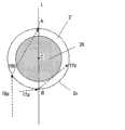
说明公开的取光棒的实施方式。图27(a)和(b)模式化地表示与本实施方式的取光棒61的中心轴平行的截面构造和与中心轴垂直的截面构造。取光棒61具备透光棒2’和在透光棒2’的内部所配置的至少一个光耦合构造3。Embodiments of the disclosed light-trapping stick will be described. 27( a ) and ( b ) schematically show a cross-sectional structure parallel to the central axis and a cross-sectional structure perpendicular to the central axis of the light-trapping
透光棒2’在与中心轴C垂直的面具有圆或椭圆的截面形状。透光棒2’与第一实施方式同样,由透射与用途相应的期望的波长的光的、或透射期望的波长域内的光的透明材料构成。The light-transmitting rod 2' has a circular or elliptical cross-sectional shape on a plane perpendicular to the central axis C. Like the first embodiment, the light-transmitting rod 2' is made of a transparent material that transmits light of a desired wavelength according to the application, or transmits light in a desired wavelength range.
在该透光棒2’的外侧按照夹隔垫片2d的方式粘接有盖板2e。因此,作为透光棒2’的表面的主面2u的大部分与缓冲层2f相接。垫片2d由气凝胶这样的比透光棒2’的折射率低的材料构成。The outer side of this light-transmitting rod 2' is bonded with a
透光棒2’的截面为圆形时,在与透光棒2’的中心轴C垂直的截面的直径D例如为0.05mm~2mm左右。按照从作为透光棒2’的主面的表面2u、在朝向中心轴C的方向上隔开距离d3以上的方式设置一个以上的光耦合构造3。优选取光棒61具备多个耦合构造3。透光棒2’具有圆或椭圆的截面形状,并且,就光耦合构造3而言,在与透光棒2’的中心轴C垂直的面,具有以中心轴C为中心的直径d=D-2×d3的圆形,且被配置在沿中心轴C方向延伸的中心区域2A内。When the cross-section of the light-transmitting rod 2' is circular, the diameter D of the cross-section perpendicular to the central axis C of the light-transmitting rod 2' is, for example, about 0.05 mm to 2 mm. One or more
光耦合构造3,在中心区域2A内,以规定的密度分别配置于轴向、径向和周向。例如,就光耦合构造3的配置的密度而言,在轴向每1mm有10~103个,在径向每1mm有10~103个,在周向每1mm有10~103个左右。中心区域的截面形状为圆形或椭圆,也可以是两个以上的轮带形状。The
光耦合构造3具备与第一实施方式的光耦合构造3相同的构造。另外,取光棒61也可以具备第二实施方式的光耦合构造3’或第三实施方式的光耦合构造3”而取代光耦合构造3。The
光耦合构造3按照使第三透光层3c的衍射光栅与透光棒2’的中心轴C平行的方式配置在中心区域2A内。光耦合构造3的中心轴C方向的长度L为3μm~100μm,与之正交的方向的长度W是L的1/3~1/10左右。The
在图27(a)和(b)中,使包围取光棒61的环境介质的折射率为1.0,透光棒2’的折射率为ns。来自环境介质的光4透过盖板2e和缓冲层2f,从透光棒2’的主面2u入射到透光棒2’的内部。缓冲层2f由与环境介质相同的介质构成,其折射率为1。另外,垫片2d的折射率也大致等于1。为了提高在盖板2e的两面和表面2u所入射的光4的透射率,也可以形成AR涂层和无反射纳米构造(蝇眼结构等)。在此,透光棒2’内部的光之中的、其传播方位和棒表面的法线所形成的夹角θ(传播角)满足sinθ<1/ns的光,称为临界角内的光;将满足sinθ≥1/ns的光称为临界角外的光。In Fig. 27(a) and (b), the refractive index of the ambient medium surrounding the light-trapping
首先,尝试观看与透光棒2’的中心轴C平行的截面的光的矢量。在该截面,透光棒2’内部的临界角内的光5a的一部分被光耦合构造3转换成临界角外的光5b,该光在表面2u发生全反射,成为在透光棒2’内部滞留的临界角外的光5c。另外,临界角内光5a的剩余的临界角内的光5a’之内的一部分被别的光耦合构造3转换成临界角外的光5b’,该光在表面2u发生全反射,成为在棒内部滞留的临界角外的光5c’。如此临界角内的光5a的全部,在设有光耦合构造3的中心区域2A内被转换成临界角外的光5b和5b’。另一方面,透光棒2’内部的临界角外的光6a,其一部分在光耦合构造3的表面发生全反射而成为临界角外的光6b,该光在表面2u发生全反射,成为在棒内部滞留的临界角外的光6c。另外,临界角外的光6a的剩余的光的一部分透过设有光耦合构造3的中心区域2A,该临界角外的光6b’在表面2u发生全反射,成为在透光棒2’内部滞留的临界角外的光6c’。另外,虽未图示,但一边在不同的光耦合构造3之间和表面2u之间发生全反射、一边在板内部滞留的临界角外的光也存在。First, try to observe the light vector of the section parallel to the central axis C of the light-transmitting rod 2'. In this cross-section, part of the light 5a within the critical angle inside the light-transmitting rod 2' is converted by the
如参照图2(a)说明的,临界角内的光5a,透过第二透光层3b的表面3q,其一部分在衍射光栅的作用下,被转换成在第三透光层3c内传播的导波光5B。其余成为透射光和衍射光,主要成为临界角内的光5a’而透过光耦合构造3、或作为反射光成为临界角内的光5r,穿过光耦合构造3。就导波光5B而言,在达到第三透光层3c的端面3S以前,其一部分沿着与临界角内的5r相同的方向被放射,成为临界角内的光5r’;剩余的作为导波从第三透光层3c的端面3S被放射,成为临界角外的光5c。另一方面,临界角外的光6a,在第二透光层3b的表面3q发生全反射,其全部成为临界角外的光6b。如此,入射到光耦合构造3的表面(第一透光层3a的表面3p和第二透光层3b的表面3q)的临界角外的光为临界角外的状态,临界角内的光其一部分被转换成临界角外的光。As explained with reference to Fig. 2 (a), the light 5a in the critical angle passes through the
接着,观看与棒的中心轴正交的截面中光的矢量。在该截面,进入棒内部的光被分为三种。穿过中心区域2A的光15a,穿过中心区域2A的外缘的光15b,并且穿过中心区域2A之外的光15c。光15a,如前述,在沿着棒的中心轴的截面内被转换成在棒内部滞留的临界角外的光。另一方面,光15b是以角度ψ入射到棒的表面2u的光,ψ满足式(3)。Next, look at the vector of the light in a section normal to the central axis of the rod. In this section, the light entering the inside of the rod is divided into three types. Light 15a that passes through the
【算式3】
当然,光15c向表面2u的入射角比ψ大。因此,如果式(4)成立,则光15b在棒的第一主面2p发生全反射,光15b、15c在与中心轴正交的截面内变成在透光棒2’内部滞留的临界角外的光。Of course, the incident angle of the light 15c to the
【算式4】
因此,符合与平行于透光棒2’的中心轴C的截面正交的截面,满足式(4),就成为用于使透光棒2’内部的全部的光在透光棒2’内部滞留的条件。Therefore, conforming to the cross-section perpendicular to the cross-section parallel to the central axis C of the light-transmitting rod 2', and satisfying the formula (4), it is used to make all the light in the light-transmitting rod 2' inside the light-transmitting rod 2' Conditions of stay.
还有,在图27的例子中,透光棒2’的主面2u经由缓冲层2f而由盖板2e覆盖。因此,水滴等的异物2g附着于盖板2e的表面,与主面2u接触得以防止。假如,异物2g与第一主面2u接触,则在该接触面,全反射的关系破坏,在透光棒2’内所封闭的临界角外的光会经由异物2g而泄漏到外部。垫片2d也与主面2u相接,但其折射率与环境介质的折射率几乎不变,因此在此接触面而全反射的关系得以维持,临界角外的光不会经由垫片2d而泄漏到外部。另外,透光棒的表面积小时,也可以不夹隔垫片2d而在盖板2e与主面2u之间形成缓冲层2f。In addition, in the example of Fig. 27, the
图28是表示取光棒61的制作步骤的模式化的剖面结构图。在图28中,以与第一至第三的实施方式相同的方法,制作图7、13、18的树脂板24、24a(和24′、24a′)。就在树脂板24、24a(和24a′)上形成光耦合构造3的衍射光栅的栅格矢量而言,以沿着z轴测量的间距为0.30μm至2.80μm的方式使各种各样的间距的衍射光栅加以组合,或者将单一的间距的衍射光栅以相对于z轴沿着各种各样的方向(例如30度和15度刻度的角度)的方式设置,或者是它们的组合也可。就光耦合构造3的大小而言,以能够使耦合的导波光尽可能沿着棒的中心轴放射的方式,将z轴方向的长度L设定为3μm~100μm,与之正交的方向的长度W设定为L的1/2~1/10左右。在该板没有衍射光栅一侧的表面薄薄地涂布粘接剂,一边在z轴的周围旋转一边卷绕,由此能够制作取光棒61的中心区域2A。再使其周围由形成有无反射纳米构造的透明的保护层包裹,取光棒61完成。FIG. 28 is a schematic cross-sectional structural view showing the manufacturing steps of the light-trapping
(第十二实施方式)(twelfth embodiment)
以下,列举出第十二至第十三实施方式,但关于盖板2e的说明与第十一实施方式相同,省略重复的说明。Hereinafter, the twelfth to thirteenth embodiments will be listed, but the description about the
说明本公开的发光装置的实施方式。图29模式化地表示本实施方式的发光装置62的截面构造。发光装置62具备取光棒61、和光源14R、14G、14B。取光棒61具备如第十一实施方式中所说明的构造。Embodiments of the light emitting device of the present disclosure will be described. FIG. 29 schematically shows a cross-sectional structure of a
在取光棒61的端面2r设有反射膜11。优选在取光棒61的端面2s侧的表面2u,设置锥度2v,且连接比透光棒2’直径小的波导28。The
光源14R、14G、14B由LD或LED等构成,例如,分别发出红、绿、蓝的光。由这些光源出射的光通过透镜会聚,向透光棒2’的表面2u照射光4R、4G、4B。这些光通过中心区域2A内的光耦合构造3而被封闭在透光棒2’内部,由于一方的端面2r被反射膜11覆盖,所以整体上成为在棒内部沿一个方向传播的导波光12。该导波光12经由棒2’的直径慢慢变小的锥度2v在无损耗下被收缩,成为在拥有细径的波导18内部传播的导波光。由此,从波导18的端面出射接近点光源的光19。光源为激光时,光4R、4G、4B是相干光,但因为来自各个光耦合构造3的光放射以离散的相位进行,所以其合成的导波光12成为非相干光。因此,出射光19也为非相干光。如果调整光4R、4G、4B的光量,则能够使出射光19成为白色光。现在,红、蓝的半导体激光器得以实现,如果使用SHG,则也能够利用绿色的激光。由这些光源合成白色光时,一般来说需要复杂的光学构成,而且由于激光特有的可干涉性还会成为闪耀的光。但是,根据本实施方式的发光装置62,能够提供在极其简单的构成下没有闪耀的更自然的白色光的点光源。The
本实施方式的情况下,需要调整的地方,是所入射的光4R、4G、4B形成的会聚光和棒2’的位置调整。图30是表示光向取光棒61入射的情况的剖面说明图,点O是棒的中心。若使透光棒2’的折射率为1.5,则与直线AOB平行的光16a,发生折射,成为大致会聚到点A的光16b。若中心区域2A的直径比透光棒2’的直径的1/1.5大,则根据式(4),光16b确实地通过中心区域2A,被封闭在透光棒2’内。相反,要描绘没有通过中心区域2A的光线有困难。例如,若考虑入射到点B而没有通过中心区域的光17b,则为此入射光线17a相对于入射面成为掠射角的光(在高数值孔径下所会聚的最外缘的光)。换言之,如果是一般的入射角的光线、即是在一般的数值孔径下所会聚的光,则其全部通过中心区域2A,被封闭在透光棒2’内。这表示入射的光4R、4G、4B与透光棒2’的位置调整可以非常粗略,显示出调整的容易性。In the case of the present embodiment, adjustments are required for the converging light formed by the
(第十三实施方式)(thirteenth embodiment)
说明本公开的发光装置其他的实施方式。图31模式化地表示本实施方式的发光装置63的截面构造。发光装置63具备取光棒61、光源14和棱镜板9。取光棒61具备如第十一实施方式中所说明的构造。Another embodiment of the light emitting device of the present disclosure will be described. FIG. 31 schematically shows a cross-sectional structure of a
在取光棒61的端面2r设有反射膜11。另外,取光棒61中没有设置光耦合构造3的部分作为波导18发挥机能。在波导18的表面2u设有棱镜板9。The
光源14由LD或LED等构成,发出可视光。该光源出射的光由透镜会聚,成为在透光棒2’内透过的光4。这些光通过中心区域2A内的光耦合构造3,被封闭在透光棒2’内部,因为一方的端面由反射膜11覆盖,所以整体上成为在透光棒2’内部沿一个方向传播的光12,成为在波导18内部传播的导波光。在波导18将棱镜板9接触地配置。在棱镜板9的内部,四面体状的棱镜10彼此邻接配置。也可以将三角柱棱镜列的板正交贴合。因为该棱镜10的折射率比棱镜板9的折射率大,所以从波导18漏出而入射棱镜板9的光发生折射,从棱镜板9出射,成为平行的出射光19。还有,也可以使棱镜板9从波导18分离,这种情况下,在波导18的表面的面向棱镜板9的一侧形成凹凸构造而使光出射。The
光源为激光时,光4为相干光,但因为来自各个光耦合构造3的光放射以离散的相位进行,所以其合成的导波光12成为非相干光。因此,出射光19也为非相干光。现在,红、蓝的半导体激光得以实现,如果使用SHG,也能够利用绿色的激光。若使用这些光源,则能够得到红、绿、蓝的线光源。例如,通过使这些线光源聚集,能够以极其简单的结构提供液晶显示器用的彩色背光。When the light source is laser light, the
【产业上的可利用性】【Industrial availability】
本公开的板和棒,可以不受水滴、尘埃和污物等的影响,跨越宽阔区域、宽阔波长范围(例如可视光全域),以全部的入射角进行光的引入,使用了它们的光接收装置对于高转换效率太阳能电池等有用,另一方面,使用了它们的光接收和发光装置,提供出新的照明和光源的形态,作为利用太阳光和照明光的循环照明、高效率的背光、非相干的白色光源有用。The plate and rod of the present disclosure can not be affected by water droplets, dust, dirt, etc., and can introduce light at all incident angles across a wide area and a wide wavelength range (for example, the entire range of visible light), using their light Receiving devices are useful for high conversion efficiency solar cells, etc. On the other hand, light receiving and light emitting devices using them provide new forms of lighting and light sources, as circular lighting using sunlight and lighting light, high-efficiency backlights , incoherent white light sources are useful.
【符号说明】【Symbol Description】
2 透光板2 Translucent panels
2’ 透光棒2’ Translucent Rod
2p 第一主面2p the first main face
2q 第二主面2q second main face
2u 表面2u surface
3、3’、3” 光耦合构造3, 3’, 3” optical coupling structure
3a 第一透光层3a The first transparent layer
3b 第二透光层3b second transparent layer
3c 第三透光层3c The third transparent layer
3d 衍射光栅3d Diffraction Grating
4 入射光4 incident light
5a,5a’ 临界角内的光5a, 5a’ Light within the critical angle
5b、5c、5b’、5c’ 临界角外的光5b, 5c, 5b’, 5c’ Light outside the critical angle
6a、6b、6c、6b’、6c’ 临界角外的光6a, 6b, 6c, 6b’, 6c’ Light outside the critical angle
9 棱镜板9 Prism plate
10 棱镜10 Prisms
11 反射膜11 reflective film
14 光源14 light sources
Claims (31)
Translated fromChineseApplications Claiming Priority (3)
| Application Number | Priority Date | Filing Date | Title |
|---|---|---|---|
| JP2011244601 | 2011-11-08 | ||
| JP2011-244601 | 2011-11-08 | ||
| PCT/JP2012/007080WO2013069248A1 (en) | 2011-11-08 | 2012-11-05 | Light acquisition sheet and rod, and light-receiving device and light-emitting device using same |
Publications (2)
| Publication Number | Publication Date |
|---|---|
| CN103270442Atrue CN103270442A (en) | 2013-08-28 |
| CN103270442B CN103270442B (en) | 2015-12-23 |
Family
ID=48289341
Family Applications (1)
| Application Number | Title | Priority Date | Filing Date |
|---|---|---|---|
| CN201280004252.0AActiveCN103270442B (en) | 2011-11-08 | 2012-11-05 | Light-taking plate and rod, and light-receiving device and light-emitting device using them |
Country Status (4)
| Country | Link |
|---|---|
| US (1) | US9316786B2 (en) |
| JP (1) | JP6238203B2 (en) |
| CN (1) | CN103270442B (en) |
| WO (1) | WO2013069248A1 (en) |
Families Citing this family (24)
| Publication number | Priority date | Publication date | Assignee | Title |
|---|---|---|---|---|
| US11726332B2 (en) | 2009-04-27 | 2023-08-15 | Digilens Inc. | Diffractive projection apparatus |
| WO2016020630A2 (en) | 2014-08-08 | 2016-02-11 | Milan Momcilo Popovich | Waveguide laser illuminator incorporating a despeckler |
| CN103270442B (en)* | 2011-11-08 | 2015-12-23 | 松下电器产业株式会社 | Light-taking plate and rod, and light-receiving device and light-emitting device using them |
| US9933684B2 (en) | 2012-11-16 | 2018-04-03 | Rockwell Collins, Inc. | Transparent waveguide display providing upper and lower fields of view having a specific light output aperture configuration |
| JP5970660B2 (en)* | 2013-06-13 | 2016-08-17 | パナソニックIpマネジメント株式会社 | Light capturing sheet and light capturing rod, and light receiving device, light emitting device and optical fiber amplifier using the same |
| CN103557936B (en)* | 2013-10-31 | 2015-10-07 | 中国科学院半导体研究所 | Laser power monitor assembly and apply its laser emitting module, image intensifer |
| WO2016042283A1 (en) | 2014-09-19 | 2016-03-24 | Milan Momcilo Popovich | Method and apparatus for generating input images for holographic waveguide displays |
| WO2016113534A1 (en) | 2015-01-12 | 2016-07-21 | Milan Momcilo Popovich | Environmentally isolated waveguide display |
| US9632226B2 (en) | 2015-02-12 | 2017-04-25 | Digilens Inc. | Waveguide grating device |
| CN113759555B (en) | 2015-10-05 | 2024-09-20 | 迪吉伦斯公司 | Waveguide Display |
| WO2018102834A2 (en) | 2016-12-02 | 2018-06-07 | Digilens, Inc. | Waveguide device with uniform output illumination |
| US10371873B2 (en)* | 2016-12-07 | 2019-08-06 | Bae Systems Information And Electronic Systems Integration Inc. | High fidelity optical beam dump |
| CN110073259A (en)* | 2016-12-15 | 2019-07-30 | 松下知识产权经营株式会社 | Waveguide piece and photo-electric conversion device |
| US10545346B2 (en) | 2017-01-05 | 2020-01-28 | Digilens Inc. | Wearable heads up displays |
| US10732569B2 (en) | 2018-01-08 | 2020-08-04 | Digilens Inc. | Systems and methods for high-throughput recording of holographic gratings in waveguide cells |
| EP3710894B1 (en) | 2018-01-08 | 2025-07-30 | Digilens Inc. | Methods for fabricating optical waveguides |
| US20200225471A1 (en) | 2019-01-14 | 2020-07-16 | Digilens Inc. | Holographic Waveguide Display with Light Control Layer |
| US20200247017A1 (en) | 2019-02-05 | 2020-08-06 | Digilens Inc. | Methods for Compensating for Optical Surface Nonuniformity |
| KR102866596B1 (en) | 2019-02-15 | 2025-09-29 | 디지렌즈 인코포레이티드. | Method and device for providing a holographic waveguide display using an integral grating |
| US20220283377A1 (en) | 2019-02-15 | 2022-09-08 | Digilens Inc. | Wide Angle Waveguide Display |
| EP3980825A4 (en) | 2019-06-07 | 2023-05-03 | Digilens Inc. | WAVEGUIDES WITH TRANSMITTING AND REFLECTING GRIDS AND RELATED MANUFACTURING PROCESSES |
| KR102775783B1 (en) | 2019-08-29 | 2025-02-28 | 디지렌즈 인코포레이티드. | Vacuum grid and method for manufacturing the same |
| WO2022150841A1 (en) | 2021-01-07 | 2022-07-14 | Digilens Inc. | Grating structures for color waveguides |
| US12158612B2 (en) | 2021-03-05 | 2024-12-03 | Digilens Inc. | Evacuated periodic structures and methods of manufacturing |
Citations (4)
| Publication number | Priority date | Publication date | Assignee | Title |
|---|---|---|---|---|
| JP2003248128A (en)* | 2002-02-25 | 2003-09-05 | Matsushita Electric Works Ltd | Optical coupler and manufacturing method thereof, and mixed optical and electrical wiring board and manufacturing method thereof |
| JP2005173116A (en)* | 2003-12-10 | 2005-06-30 | Dainippon Printing Co Ltd | Optical circuit member and manufacturing method thereof |
| WO2010151253A1 (en)* | 2009-06-24 | 2010-12-29 | University Of Rochester | Dimpled light collection and concentration system, components thereof, and methods |
| JP2011222735A (en)* | 2010-04-09 | 2011-11-04 | Nisshinbo Mechatronics Inc | Inspection method and inspection device for solar battery |
Family Cites Families (37)
| Publication number | Priority date | Publication date | Assignee | Title |
|---|---|---|---|---|
| US3939439A (en)* | 1974-12-17 | 1976-02-17 | Nasa | Diffused waveguiding capillary tube with distributed feedback for a gas laser |
| JPH05224018A (en)* | 1991-07-30 | 1993-09-03 | Nippondenso Co Ltd | Light guide device |
| US5187760A (en)* | 1992-01-23 | 1993-02-16 | General Instrument Corporation | Wavelength selective coupler for high power optical communications |
| US5877874A (en)* | 1995-08-24 | 1999-03-02 | Terrasun L.L.C. | Device for concentrating optical radiation |
| JPH10251038A (en) | 1997-03-14 | 1998-09-22 | Matsushita Electric Works Ltd | Production of optical fiber |
| KR100289042B1 (en)* | 1997-12-23 | 2001-05-02 | 이계철 | Vertically coupled wavelength variable optical fiber having double lattice structure |
| US6274860B1 (en)* | 1999-05-28 | 2001-08-14 | Terrasun, Llc | Device for concentrating optical radiation |
| US6985656B2 (en)* | 2000-03-16 | 2006-01-10 | Lightsmyth Technologies Inc | Temperature-compensated planar waveguide optical apparatus |
| US7194164B2 (en)* | 2000-03-16 | 2007-03-20 | Lightsmyth Technologies Inc | Distributed optical structures with improved diffraction efficiency and/or improved optical coupling |
| US6365428B1 (en)* | 2000-06-15 | 2002-04-02 | Sandia Corporation | Embedded high-contrast distributed grating structures |
| JP2003066203A (en)* | 2001-08-28 | 2003-03-05 | Hitachi Maxell Ltd | Method for forming fine uneven structure and member having the unevenness |
| US6876791B2 (en)* | 2001-09-03 | 2005-04-05 | Sumitomo Electric Industries, Ltd. | Diffraction grating device |
| WO2004012273A1 (en)* | 2002-02-15 | 2004-02-05 | Biosynergetics, Inc. | An electromagnetic radiation collector and transport system |
| US6885792B2 (en)* | 2002-09-24 | 2005-04-26 | Furukawa Electric North America Inc. | Wavelength monitoring optical fibers using detection in the near field |
| US7065271B2 (en)* | 2002-10-25 | 2006-06-20 | Intel Corporation | Optical grating coupler |
| JP2004151182A (en) | 2002-10-29 | 2004-05-27 | Toppan Printing Co Ltd | Light guide type diffraction grating display |
| US7349612B2 (en) | 2003-01-28 | 2008-03-25 | Nippon Sheet Glass Company, Limited | Optical element, optical circuit provided with the optical element, and method for producing the optical element |
| JP2005037872A (en)* | 2003-01-28 | 2005-02-10 | Nippon Sheet Glass Co Ltd | Optical element, optical circuit including the same, and optical demultiplexer |
| US7418170B2 (en) | 2004-03-29 | 2008-08-26 | Sony Corporation | Optical device and virtual image display device |
| JP2007538292A (en)* | 2004-05-18 | 2007-12-27 | サイファージェン バイオシステムズ インコーポレイテッド | Integrated optical waveguide sensor with reduced signal modulation |
| JP4064378B2 (en) | 2004-07-26 | 2008-03-19 | 日本電信電話株式会社 | Method and apparatus for coupling external light in waveguide hologram |
| US7573640B2 (en)* | 2005-04-04 | 2009-08-11 | Mirage Innovations Ltd. | Multi-plane optical apparatus |
| US7639911B2 (en)* | 2005-12-08 | 2009-12-29 | Electronics And Telecommunications Research Institute | Optical device having optical waveguide including organic Bragg grating sheet |
| US7854505B2 (en)* | 2006-03-15 | 2010-12-21 | The Board Of Trustees Of The University Of Illinois | Passive and active photonic crystal structures and devices |
| JP2008176302A (en) | 2006-12-22 | 2008-07-31 | Nippon Zeon Co Ltd | Optical element |
| JP2010210235A (en)* | 2007-07-03 | 2010-09-24 | Asahi Glass Co Ltd | Raindrop detecting system |
| ES2368043B1 (en)* | 2008-04-29 | 2012-10-15 | Consejo Superior De Investigaciones Científicas | Diffraction network coupler and system and procedure for the characterization of a specimen through its light coupling to it. |
| US7817885B1 (en)* | 2009-06-24 | 2010-10-19 | University Of Rochester | Stepped light collection and concentration system, components thereof, and methods |
| US8267583B2 (en)* | 2009-10-19 | 2012-09-18 | Oracle America, Inc. | Three-dimensional macro-chip including optical interconnects |
| JP5942283B2 (en) | 2010-08-25 | 2016-06-29 | パナソニックIpマネジメント株式会社 | Reflector for lighting equipment |
| EP2626729A4 (en)* | 2010-10-04 | 2017-11-15 | Panasonic Intellectual Property Management Co., Ltd. | Light acquisition sheet and rod, and light receiving device and light emitting device each using the light acquisition sheet or rod |
| TWI476483B (en)* | 2011-03-31 | 2015-03-11 | Chi Mei Materials Technology Corp | Display device and liquid crystal display device |
| WO2013069249A1 (en)* | 2011-11-08 | 2013-05-16 | パナソニック株式会社 | Light-receiving device comprising light acquisition sheet |
| CN103270442B (en)* | 2011-11-08 | 2015-12-23 | 松下电器产业株式会社 | Light-taking plate and rod, and light-receiving device and light-emitting device using them |
| WO2013069250A1 (en)* | 2011-11-08 | 2013-05-16 | パナソニック株式会社 | Light acquisition sheet, and light-receiving device and light-emitting device using same |
| CN103403592B (en)* | 2011-11-29 | 2016-10-19 | 松下知识产权经营株式会社 | Light-taking plate and rod, and light-receiving device and light-emitting device using them |
| JP5970660B2 (en)* | 2013-06-13 | 2016-08-17 | パナソニックIpマネジメント株式会社 | Light capturing sheet and light capturing rod, and light receiving device, light emitting device and optical fiber amplifier using the same |
- 2012
- 2012-11-05CNCN201280004252.0Apatent/CN103270442B/enactiveActive
- 2012-11-05JPJP2013515447Apatent/JP6238203B2/enactiveActive
- 2012-11-05WOPCT/JP2012/007080patent/WO2013069248A1/enactiveApplication Filing
- 2013
- 2013-07-23USUS13/948,462patent/US9316786B2/enactiveActive
Patent Citations (4)
| Publication number | Priority date | Publication date | Assignee | Title |
|---|---|---|---|---|
| JP2003248128A (en)* | 2002-02-25 | 2003-09-05 | Matsushita Electric Works Ltd | Optical coupler and manufacturing method thereof, and mixed optical and electrical wiring board and manufacturing method thereof |
| JP2005173116A (en)* | 2003-12-10 | 2005-06-30 | Dainippon Printing Co Ltd | Optical circuit member and manufacturing method thereof |
| WO2010151253A1 (en)* | 2009-06-24 | 2010-12-29 | University Of Rochester | Dimpled light collection and concentration system, components thereof, and methods |
| JP2011222735A (en)* | 2010-04-09 | 2011-11-04 | Nisshinbo Mechatronics Inc | Inspection method and inspection device for solar battery |
Also Published As
| Publication number | Publication date |
|---|---|
| US9316786B2 (en) | 2016-04-19 |
| JPWO2013069248A1 (en) | 2015-04-02 |
| WO2013069248A1 (en) | 2013-05-16 |
| JP6238203B2 (en) | 2017-11-29 |
| CN103270442B (en) | 2015-12-23 |
| US20130299684A1 (en) | 2013-11-14 |
Similar Documents
| Publication | Publication Date | Title |
|---|---|---|
| CN103270442B (en) | Light-taking plate and rod, and light-receiving device and light-emitting device using them | |
| CN103403592B (en) | Light-taking plate and rod, and light-receiving device and light-emitting device using them | |
| CN103097930B (en) | Get tabula rasa and rod and the optical pickup apparatus and the light-emitting device that employ them | |
| CN103261933B (en) | Light-taking plate and light-receiving device and light-emitting device using it | |
| CN103261936B (en) | Light-receiving device with light-trapping plate | |
| JP5970660B2 (en) | Light capturing sheet and light capturing rod, and light receiving device, light emitting device and optical fiber amplifier using the same | |
| CN111226148B (en) | Waveguide sheet and photoelectric conversion device | |
| WO2022030543A1 (en) | Light incoupling tape, related method and uses | |
| JP2014206680A (en) | Light-collecting sheet, photoreceiver using the same and light-emitting device |
Legal Events
| Date | Code | Title | Description |
|---|---|---|---|
| C06 | Publication | ||
| PB01 | Publication | ||
| C10 | Entry into substantive examination | ||
| SE01 | Entry into force of request for substantive examination | ||
| C14 | Grant of patent or utility model | ||
| GR01 | Patent grant | ||
| C41 | Transfer of patent application or patent right or utility model | ||
| TR01 | Transfer of patent right | Effective date of registration:20151231 Address after:Japan Osaka Patentee after:PANASONIC INTELLECTUAL PROPERTY MANAGEMENT Co.,Ltd. Address before:Osaka Japan Patentee before:Matsushita Electric Industrial Co.,Ltd. |