CN103259190A - Annular semiconductor laser of vertical coupling structure and preparing method thereof - Google Patents
Annular semiconductor laser of vertical coupling structure and preparing method thereofDownload PDFInfo
- Publication number
- CN103259190A CN103259190ACN2013101749018ACN201310174901ACN103259190ACN 103259190 ACN103259190 ACN 103259190ACN 2013101749018 ACN2013101749018 ACN 2013101749018ACN 201310174901 ACN201310174901 ACN 201310174901ACN 103259190 ACN103259190 ACN 103259190A
- Authority
- CN
- China
- Prior art keywords
- layer
- type
- wafer
- barrier layer
- ring resonator
- Prior art date
- Legal status (The legal status is an assumption and is not a legal conclusion. Google has not performed a legal analysis and makes no representation as to the accuracy of the status listed.)
- Pending
Links
- 239000004065semiconductorSubstances0.000titleclaimsabstractdescription45
- 238000000034methodMethods0.000titleclaimsabstractdescription34
- 238000010168coupling processMethods0.000titleclaimsabstractdescription20
- 238000005859coupling reactionMethods0.000titleclaimsabstractdescription20
- 230000008878couplingEffects0.000titleclaimsabstractdescription19
- 230000004888barrier functionEffects0.000claimsabstractdescription32
- 238000005530etchingMethods0.000claimsabstractdescription24
- 230000008569processEffects0.000claimsabstractdescription19
- 238000005229chemical vapour depositionMethods0.000claimsabstractdescription10
- 229910052751metalInorganic materials0.000claimsabstractdescription9
- 239000002184metalSubstances0.000claimsabstractdescription9
- 229920000642polymerPolymers0.000claimsdescription28
- 239000000463materialSubstances0.000claimsdescription19
- 238000002360preparation methodMethods0.000claimsdescription17
- 229910000980Aluminium gallium arsenideInorganic materials0.000claimsdescription16
- 238000005516engineering processMethods0.000claimsdescription14
- 229910004298SiO 2Inorganic materials0.000claimsdescription10
- 230000012010growthEffects0.000claimsdescription10
- 229910001218Gallium arsenideInorganic materials0.000claimsdescription9
- 239000013078crystalSubstances0.000claimsdescription9
- CSCPPACGZOOCGX-UHFFFAOYSA-NAcetoneChemical compoundCC(C)=OCSCPPACGZOOCGX-UHFFFAOYSA-N0.000claimsdescription8
- IJGRMHOSHXDMSA-UHFFFAOYSA-NAtomic nitrogenChemical compoundN#NIJGRMHOSHXDMSA-UHFFFAOYSA-N0.000claimsdescription8
- LFQSCWFLJHTTHZ-UHFFFAOYSA-NEthanolChemical compoundCCOLFQSCWFLJHTTHZ-UHFFFAOYSA-N0.000claimsdescription8
- KRHYYFGTRYWZRS-UHFFFAOYSA-NFluoraneChemical compoundFKRHYYFGTRYWZRS-UHFFFAOYSA-N0.000claimsdescription8
- 239000000758substrateSubstances0.000claimsdescription8
- 238000004528spin coatingMethods0.000claimsdescription7
- 238000005566electron beam evaporationMethods0.000claimsdescription5
- 229910052737goldInorganic materials0.000claimsdescription5
- 238000001755magnetron sputter depositionMethods0.000claimsdescription5
- BQCADISMDOOEFD-UHFFFAOYSA-NSilverChemical compound[Ag]BQCADISMDOOEFD-UHFFFAOYSA-N0.000claimsdescription4
- 239000008367deionised waterSubstances0.000claimsdescription4
- 229910052757nitrogenInorganic materials0.000claimsdescription4
- 229920002120photoresistant polymerPolymers0.000claimsdescription4
- 229910052709silverInorganic materials0.000claimsdescription4
- 239000004332silverSubstances0.000claimsdescription4
- 229910000530Gallium indium arsenideInorganic materials0.000claimsdescription3
- 239000002131composite materialSubstances0.000claimsdescription3
- 238000012545processingMethods0.000claimsdescription3
- 230000000149penetrating effectEffects0.000claims2
- 238000001259photo etchingMethods0.000claims2
- 238000005260corrosionMethods0.000claims1
- 230000007797corrosionEffects0.000claims1
- 230000008020evaporationEffects0.000claims1
- 238000001704evaporationMethods0.000claims1
- 238000010438heat treatmentMethods0.000claims1
- 238000001459lithographyMethods0.000claims1
- 239000002002slurrySubstances0.000claims1
- 238000004544sputter depositionMethods0.000claims1
- VYPSYNLAJGMNEJ-UHFFFAOYSA-NSilicium dioxideChemical compoundO=[Si]=OVYPSYNLAJGMNEJ-UHFFFAOYSA-N0.000abstractdescription12
- 238000001451molecular beam epitaxyMethods0.000abstractdescription7
- 229910052681coesiteInorganic materials0.000abstractdescription6
- 229910052906cristobaliteInorganic materials0.000abstractdescription6
- 239000000377silicon dioxideSubstances0.000abstractdescription6
- 235000012239silicon dioxideNutrition0.000abstractdescription6
- 229910052682stishoviteInorganic materials0.000abstractdescription6
- 229910052905tridymiteInorganic materials0.000abstractdescription6
- 238000005253claddingMethods0.000description25
- 230000003287optical effectEffects0.000description13
- 238000000206photolithographyMethods0.000description10
- 150000001875compoundsChemical class0.000description9
- 238000001020plasma etchingMethods0.000description8
- 238000005036potential barrierMethods0.000description6
- 238000003776cleavage reactionMethods0.000description4
- 238000010586diagramMethods0.000description4
- 238000004519manufacturing processMethods0.000description4
- 238000000623plasma-assisted chemical vapour depositionMethods0.000description4
- 230000007017scissionEffects0.000description4
- 239000004642PolyimideSubstances0.000description3
- UMIVXZPTRXBADB-UHFFFAOYSA-NbenzocyclobuteneChemical compoundC1=CC=C2CCC2=C1UMIVXZPTRXBADB-UHFFFAOYSA-N0.000description3
- 230000005540biological transmissionEffects0.000description3
- 238000006243chemical reactionMethods0.000description3
- 229910021641deionized waterInorganic materials0.000description3
- 229920001721polyimidePolymers0.000description3
- XLYOFNOQVPJJNP-UHFFFAOYSA-NwaterChemical compoundOXLYOFNOQVPJJNP-UHFFFAOYSA-N0.000description3
- YCKRFDGAMUMZLT-UHFFFAOYSA-NFluorine atomChemical compound[F]YCKRFDGAMUMZLT-UHFFFAOYSA-N0.000description2
- 229920002319Poly(methyl acrylate)Polymers0.000description2
- 230000008859changeEffects0.000description2
- 230000007547defectEffects0.000description2
- 238000011161developmentMethods0.000description2
- 229910052731fluorineInorganic materials0.000description2
- 239000011737fluorineSubstances0.000description2
- 230000010354integrationEffects0.000description2
- 229910002059quaternary alloyInorganic materials0.000description2
- 230000034655secondary growthEffects0.000description2
- 230000009286beneficial effectEffects0.000description1
- 238000000151depositionMethods0.000description1
- 230000008021depositionEffects0.000description1
- 238000013461designMethods0.000description1
- 238000010894electron beam technologyMethods0.000description1
- 238000009616inductively coupled plasmaMethods0.000description1
- 238000004377microelectronicMethods0.000description1
- 238000012986modificationMethods0.000description1
- 230000004048modificationEffects0.000description1
- 238000000465mouldingMethods0.000description1
- 230000005693optoelectronicsEffects0.000description1
- 150000002902organometallic compoundsChemical class0.000description1
- 239000002861polymer materialSubstances0.000description1
- 230000001568sexual effectEffects0.000description1
- 238000000992sputter etchingMethods0.000description1
Images


Landscapes
- Semiconductor Lasers (AREA)
Abstract
Description
Translated fromChinese技术领域technical field
本发明涉及半导体激光器领域,特别涉及一种垂直耦合结构的半导体环形激光器及其制备方法。The invention relates to the field of semiconductor lasers, in particular to a semiconductor ring laser with a vertical coupling structure and a preparation method thereof.
背景技术Background technique
半导体环形激光器利用闭合波导环路作为谐振腔,不需要解理面或光栅提供光反馈,可与晶向任意偏转,结构紧凑、工艺简单、可靠性高、与现有微电子工艺完全兼容,可实现高密度集成。它不仅可以实现可调谐光源、光开关、波长转换等功能,而且可构建全光逻辑和光随机存储器等光网络中的关键器件和组件,解决了单片光电集成回路中器件结构和制备工艺的兼容性问题。因此,可广泛地应用于可调谐集成光源、光随机存储器、全光逻辑、光开关和波长变换等一系列光器件和组件中。The semiconductor ring laser uses a closed waveguide loop as a resonant cavity, does not need a cleavage surface or a grating to provide optical feedback, and can be deflected arbitrarily with the crystal direction. It has a compact structure, simple process, high reliability, and is fully compatible with existing microelectronics processes. Achieve high-density integration. It can not only realize tunable light source, optical switch, wavelength conversion and other functions, but also can construct key devices and components in optical networks such as all-optical logic and optical random access memory, and solve the compatibility of device structure and manufacturing process in monolithic optoelectronic integrated circuits. sexual issues. Therefore, it can be widely used in a series of optical devices and components such as tunable integrated light source, optical random access memory, all-optical logic, optical switch and wavelength conversion.
侧向耦合结构的半导体环形激光器的环形谐振腔和输出条形波导处在同一平面,两者的材料结构完全相同,因此,光输出时条形波导产生很高的损耗。另外,为了实现条形波导与环形谐振腔间的有效耦合,二者的耦合间距极小(0.1~0.3μm),因而必须使用电子束曝光、感应耦合等离子体(ICP)刻蚀等半导体工艺设备,这不仅使得器件制备成本昂贵,而且工艺精度也难以控制。与此相比,垂直耦合结构的半导体环形激光器的环形谐振腔和输出条形波导处于不同平面,可以独立优化设计,因而可以提高器件性能,降低工艺难度。The ring resonator of the side-coupling semiconductor ring laser and the output strip waveguide are in the same plane, and the material structure of the two is exactly the same, so the strip waveguide produces high loss when the light is output. In addition, in order to achieve effective coupling between the strip waveguide and the ring resonator, the coupling distance between the two is extremely small (0.1-0.3 μm), so semiconductor process equipment such as electron beam exposure and inductively coupled plasma (ICP) etching must be used , which not only makes device fabrication expensive, but also difficult to control the process precision. In contrast, the ring resonator and the output strip waveguide of the semiconductor ring laser with vertical coupling structure are in different planes, and the design can be optimized independently, which can improve device performance and reduce process difficulty.
已有的垂直耦合结构采用分子束外延(MBE)或金属有机化合物化学气相淀积(MOCVD)二次生长技术分别生长环形谐振腔和条形波导的材料结构,这种带图形的二次生长技术,增加了工艺制备的难度和复杂度。另外,也有采用键合工艺实现微环谐振腔和条形波导的垂直耦合环形激光器,但器件的可靠性和稳定性相对较差。The existing vertical coupling structure uses molecular beam epitaxy (MBE) or metal organic compound chemical vapor deposition (MOCVD) secondary growth technology to grow the material structure of ring resonator and strip waveguide respectively. This secondary growth technology with pattern , increasing the difficulty and complexity of the process preparation. In addition, there are also vertically coupled ring lasers that use a bonding process to realize microring resonators and strip waveguides, but the reliability and stability of the devices are relatively poor.
发明内容Contents of the invention
本发明提供了一种垂直耦合结构的半导体环形激光器及其制备方法,本发明降低了工艺制备的难度和复杂度,提高了器件的可靠性和稳定性,详见下文描述:The present invention provides a semiconductor ring laser with a vertical coupling structure and a preparation method thereof. The present invention reduces the difficulty and complexity of process preparation and improves the reliability and stability of the device. See the following description for details:
一种垂直耦合结构的半导体环形激光器,所述半导体环形激光器包括:由半导体材料制成的有源环形谐振腔,所述有源环形谐振腔为:脊型波导或条形波导构成的任意闭合环路,A semiconductor ring laser with a vertical coupling structure, the semiconductor ring laser includes: an active ring resonator made of semiconductor material, the active ring resonator is: any closed ring formed by a ridge waveguide or a strip waveguide road,
所述有源环形谐振腔上制作有P型电极和N型电极,用于实现半导体材料的光激射,所述有源环形谐振腔内的激射光通过垂直耦合器耦合进条形直波导,所述条形直波导输出所述激射光。A P-type electrode and an N-type electrode are fabricated on the active ring resonant cavity for lasing semiconductor materials, and the lasing light in the active ring resonant cavity is coupled into a strip-shaped straight waveguide through a vertical coupler, The strip straight waveguide outputs the lasing light.
所述有源环形谐振腔采用Ⅲ-Ⅴ族化合物半导体材料体系;The active ring resonator adopts a III-V compound semiconductor material system;
所述垂直耦合器采用聚合物和Ⅲ-Ⅴ族化合物半导体组成的复合材料体系。The vertical coupler adopts a composite material system composed of polymer and III-V compound semiconductor.
所述垂直耦合器具体为:功率耦合效率为1-5%的垂直耦合器。The vertical coupler is specifically: a vertical coupler with a power coupling efficiency of 1-5%.
所述条形直波导与输出端面法线呈5~15°偏转。The strip-shaped straight waveguide is deflected by 5-15° with respect to the normal line of the output end face.
一种垂直耦合结构的半导体环形激光器的制备方法,所述方法包括以下步骤:A kind of preparation method of the semiconductor ring laser of vertical coupling structure, described method comprises the following steps:
1)在100晶向的N型衬底上,用金属有机物化学气相淀积或分子束外延方法依次生长预设厚度和浓度的N型下包层、第一渐变折射率限制层、第一势垒层、多量子阱有源层、第二势垒层、第二渐变折射率限制层、P型上包层和P型接触层;1) On the N-type substrate with 100 crystal orientation, the N-type lower cladding layer, the first graded index confinement layer, the first potential Barrier layer, multi-quantum well active layer, second potential barrier layer, second graded refractive index confinement layer, P-type upper cladding layer and P-type contact layer;
2)外延材料生长完成后,得到制备所述有源环形谐振腔所需的外延晶片,将晶片依次用丙酮、乙醇和去离子水清洗,用高纯氮气吹干;2) After the growth of the epitaxial material is completed, the epitaxial wafer required for the preparation of the active ring resonator is obtained, and the wafer is sequentially cleaned with acetone, ethanol and deionized water, and dried with high-purity nitrogen;
3)在晶片表面淀积一层SiO2薄膜,利用所述有源环形谐振腔的光学掩膜版进行光刻,并在晶片上制备出SiO2图形;3) Deposit a layer ofSiO2 film on the surface of the wafer, use the optical mask of the active ring resonator to perform photolithography, and prepareSiO2 patterns on the wafer;
4)用所述SiO2图形作掩膜刻蚀若干外延层,刻蚀深度小于等于第一高度,且大于等于第二高度,将所述有源环形谐振腔转移到晶片上;4) Using theSiO2 pattern as a mask to etch several epitaxial layers, the etching depth is less than or equal to the first height and greater than or equal to the second height, and transferring the active ring resonator to the wafer;
其中,所述第一高度为:P型接触层上表面至N型下包层上表面的距离;所述第二高度为:P型接触层上表面至第二势垒层上表面的距离;Wherein, the first height is: the distance from the upper surface of the P-type contact layer to the upper surface of the N-type lower cladding layer; the second height is: the distance from the upper surface of the P-type contact layer to the upper surface of the second barrier layer;
5)采用缓冲氢氟酸溶液腐蚀去除所述SiO2图形;5) removing the SiO2 pattern by etching with a buffered hydrofluoric acid solution;
6)在晶片的上表面旋涂聚合物介质,旋涂厚度高于所述刻蚀深度,并加热固化,之后刻蚀所述聚合物介质至所述有源环形谐振腔的表面,完成晶片表面平坦化;6) Spin-coat a polymer medium on the upper surface of the wafer with a thickness higher than the etching depth, heat and solidify, and then etch the polymer medium to the surface of the active ring resonant cavity to complete the wafer surface flattened;
7)在晶片正面旋涂光刻胶,光刻制备出P型电极图形窗口,接着溅射金属Ti和Au,采用剥离工艺制备出P型电极;7) Spin-coat photoresist on the front of the wafer, and prepare a P-type electrode pattern window by photolithography, then sputter metal Ti and Au, and prepare a P-type electrode by lift-off process;
8)在所述有源微环谐振腔上旋涂聚合物,通过光刻步骤制备出单模传输的聚合物条形直波导;8) Spin-coating a polymer on the active microring resonator, and preparing a polymer strip-shaped straight waveguide for single-mode transmission through photolithography steps;
9)对晶片进行减薄处理,利用磁控溅射或电子束蒸发技术在晶片背面蒸镀AuGeNi和Au,形成N型电极;9) Thinning the wafer, using magnetron sputtering or electron beam evaporation technology to evaporate AuGeNi and Au on the back of the wafer to form N-type electrodes;
10)将晶片沿划片槽解理成窄条状,并用银浆粘贴在管座上,进行引线键合,最后封装在管壳中,完成聚合物和Ⅲ-Ⅴ族化合物半导体环形激光器的制备。10) Cleave the wafer into narrow strips along the dicing groove, paste it on the stem with silver paste, perform wire bonding, and finally package it in a tube case to complete the preparation of polymer and III-V compound semiconductor ring lasers.
当制备InP基半导体环形激光器时,步骤1)的操作过程具体为:When preparing an InP-based semiconductor ring laser, the operation process of step 1) is specifically:
在100晶向的N型InP衬底上,用金属有机物化学气相淀积或分子束外延方法生长N型InP下包层;On the N-type InP substrate with 100 crystal orientation, the N-type InP lower cladding layer is grown by metal-organic chemical vapor deposition or molecular beam epitaxy;
依据预设厚度和浓度依次生长AlGaInAs四元系材料的第一渐变折射率限制层、第一势垒层、AlGaInAs多量子阱有源层、第二势垒层和第二渐变折射率限制层;growing the first graded index confinement layer, the first barrier layer, the AlGaInAs multi-quantum well active layer, the second barrier layer and the second graded index confinement layer of the AlGaInAs quaternary system material in sequence according to the preset thickness and concentration;
生长P型InP上包层,最后生长InGaAs接触层。A P-type InP upper cladding layer is grown, and finally an InGaAs contact layer is grown.
当制备GaAs基半导体环形激光器时,步骤1)的操作过程具体为:When preparing a GaAs-based semiconductor ring laser, the operation process of step 1) is specifically:
在100晶向的N型GaAs衬底上用金属有机物化学气相淀积或分子束外延方法生长N型AlGaAs下包层;The N-type AlGaAs lower cladding layer is grown on the N-type GaAs substrate with a 100-crystal orientation by metal-organic chemical vapor deposition or molecular beam epitaxy;
依次生长AlGaAs三元系材料的第一渐变折射率限制层、第一势垒层、AlGaAs多量子阱有源层、第二势垒层和第二渐变折射率限制层;sequentially growing the first graded index confinement layer, the first barrier layer, the AlGaAs multi-quantum well active layer, the second barrier layer and the second graded index confinement layer of the AlGaAs ternary system material;
生长P型AlGaAs上包层,最后生长GaAs接触层。A P-type AlGaAs upper cladding layer is grown, and finally a GaAs contact layer is grown.
本发明提供的技术方案的有益效果是:The beneficial effects of the technical solution provided by the invention are:
1)采用本技术方案实现的环形激光器不需要解理端面或光栅提供光反馈,结构简单、紧凑,易与其他器件单片集成,实现功能更丰富的器件或组件。1) The ring laser realized by this technical solution does not need to cleavage the end face or the grating to provide optical feedback. It has a simple and compact structure, and is easy to monolithically integrate with other devices to realize more functional devices or components.
2)在Ⅲ-Ⅴ族化合物半导体有源环形谐振腔上制备低损耗的聚合物光波导,将Ⅲ-Ⅴ族化合物半导体优越的发光特性和聚合物波导易成型、损耗小的优点结合在一起,可实现高性能、低损耗的环形激光器。2) Prepare a low-loss polymer optical waveguide on the III-V compound semiconductor active ring resonator, combining the superior light-emitting characteristics of the III-V compound semiconductor with the advantages of easy molding and low loss of the polymer waveguide, A high-performance, low-loss ring laser can be realized.
3)采用垂直耦合结构实现的环形激光器属于三维(3D)集成器件,可有效地缩减了器件横向尺寸,有利于实现器件的高密度集成。3) The ring laser realized by the vertical coupling structure is a three-dimensional (3D) integrated device, which can effectively reduce the lateral size of the device and facilitate the high-density integration of the device.
4)采用本技术方案实现的环形激光器具有工艺简单、成本低、器件性能稳定及可靠性高等优点。4) The ring laser realized by this technical solution has the advantages of simple process, low cost, stable device performance and high reliability.
附图说明Description of drawings
图1:本发明半导体环形激光器的平面结构示意图;Fig. 1: the plane structure schematic diagram of semiconductor ring laser of the present invention;
图2:本发明有源环形谐振腔的垂直结构示意图;Figure 2: A schematic diagram of the vertical structure of the active ring resonant cavity of the present invention;
图3:本发明半导体环形激光器的三维结构示意图。Fig. 3: Schematic diagram of the three-dimensional structure of the semiconductor ring laser of the present invention.
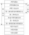
附图中,各部件所列列表如下:In the accompanying drawings, the list of each component is as follows:


具体实施方式Detailed ways
为使本发明的目的、技术方案和优点更加清楚,下面将结合附图对本发明实施方式作进一步地详细描述。In order to make the object, technical solution and advantages of the present invention clearer, the implementation manner of the present invention will be further described in detail below in conjunction with the accompanying drawings.
参见图1,一种垂直耦合结构的半导体环形激光器,包括:由半导体材料制成的有源环形谐振腔1,有源环形谐振腔1上制作有P型电极4和N型电极5,用于实现半导体材料的光激射,有源环形谐振腔1内的激射光通过垂直耦合器2耦合进条形直波导3,条形直波导3输出激射光。Referring to Fig. 1, a semiconductor ring laser with a vertically coupled structure includes: an
具体实现时,有源环形谐振腔1为:脊型波导或条形波导构成的任意闭合环路,有源环形谐振腔1的有效折射率和物理长度决定了半导体环形激光器的输出波长。In actual implementation, the
其中,有源环形谐振腔1采用Ⅲ-Ⅴ族化合物半导体材料体系,条形直波导3采用低损耗、折射率可调的聚合物材料,垂直耦合器2采用聚合物和Ⅲ-Ⅴ族化合物半导体组成的复合材料体系。Among them, the
为了降低有源环形谐振腔1的输出损耗,优选功率耦合效率为1-5%的垂直耦合器2。In order to reduce the output loss of the
为了降低输出端面的光反射,避免条形直波导3内形成有效的光学谐振,条形直波导3与输出端面法线呈5~15°偏转。In order to reduce light reflection on the output end face and avoid effective optical resonance in the strip-shaped
实施例1Example 1
参见图2和图3,InP基半导体环形激光器的制备过程如下:Referring to Figure 2 and Figure 3, the fabrication process of the InP-based semiconductor ring laser is as follows:
1、在(100)晶向的N型InP衬底6上,用金属有机物化学气相淀积或分子束外延方法生长厚度1000~2000nm、掺杂浓度1×1018cm-3的N型InP下包层7;该InP下包层7同时兼作外延生长的缓冲层,以降低在此之上外延生长薄层的缺陷密度。1. On the N-
2、依次生长AlGaInAs四元系材料的第一渐变折射率限制层8、第一势垒层9、AlGaInAs多量子阱有源层10、第二势垒层11和第二渐变折射率限制层12;2. Sequentially grow the first graded-
其中,第一渐变折射率限制层8的厚度50nm、掺杂浓度1×1018cm-3;第一势垒层9的厚度5×10nm;AlGaInAs多量子阱有源层10的厚度5×6nm;第二势垒层11的厚度10nm;第二渐变折射率限制层12的厚度50nm、掺杂浓度1×1018cm-3。Among them, the thickness of the first graded
其中,第一势垒层9、AlGaInAs多量子阱有源层10和第二势垒层11不进行任何掺杂。Wherein, the first
3、生长厚度1000~2000nm、掺杂浓度1×1018cm-3的P型InP上包层13,最后生长厚度100~200nm、掺杂浓度>1×1019cm-3的InGaAs接触层,以降低P型电极的接触电阻。3. Growing a P-type InP upper cladding layer 13 with a thickness of 1000-2000 nm and a doping concentration of 1×1018 cm-3 , and finally growing an InGaAs contact layer with a thickness of 100-200 nm and a doping concentration of >1×1019 cm-3 , To reduce the contact resistance of the P-type electrode.
4、外延材料生长完成后,得到制备有源环形谐振腔1所需的外延晶片,将晶片依次用丙酮、乙醇和去离子水清洗,用高纯氮气吹干;4. After the growth of the epitaxial material is completed, the epitaxial wafer required for the preparation of the
5、利用等离子体增强化学气相沉淀积(PECVD)在晶片表面淀积一层结构致密、厚度在500~1500nm的SiO2薄膜,利用有源环形谐振腔的光学掩膜版进行光刻,并用反应离子刻蚀(RIE)方法在晶片上制备出SiO2图形。5. Use plasma enhanced chemical vapor deposition (PECVD) to deposit a layer of SiO2 film with a dense structure and a thickness of 500-1500nm on the surface of the wafer, use the optical mask of the active ring resonant cavity for photolithography, and use the reaction SiO2 patterns were prepared on the wafer by ion etching (RIE) method.
6、用SiO2图形作掩膜,用电感耦合反应离子刻蚀(ICP-RIE)技术刻蚀若干外延层,刻蚀深度小于等于第一高度,且大于等于第二高度,将有源环形谐振腔1转移到晶片上;6. Use the SiO2 pattern as a mask, etch several epitaxial layers with inductively coupled reactive ion etching (ICP-RIE) technology, the etching depth is less than or equal to the first height, and greater than or equal to the second height, and the active annular
具体实现时,N型下包层7、第一渐变折射率限制层8、第一势垒层9、AlGaInAs多量子阱有源层10、第二势垒层11、第二渐变折射率限制层12、P型上包层13和P型接触层14分别作为外延层,通过第一和第二刻蚀深度确定刻蚀外延层的范围,刻蚀深度的具体取值根据实际应用中需要确定,本发明实施例对此不作限制。In specific implementation, the N-type
其中,第一高度为:P型接触层14上表面至N型下包层7上表面的距离;第二高度为:P型接触层14上表面至第二势垒层11上表面的距离,例如:第一高度为3500nm时,对P型接触层14、P型上包层13、第二渐变折射率限制层12、第二势垒层11、AlGaInAs多量子阱有源层10、第一势垒层9、第一渐变折射率限制层8及部分N型下包层7进行刻蚀;第二高度为1100nm时,对P型接触层14、P型上包层13和第二渐变折射率限制层12进行刻蚀。Wherein, the first height is: the distance from the upper surface of the P-type contact layer 14 to the upper surface of the N-type
7、采用缓冲氢氟酸溶液(HF)腐蚀去除SiO2图形;7. Use buffered hydrofluoric acid solution (HF) to etch and remove SiO2 graphics;
8、在晶片的上表面旋涂聚合物介质15,旋涂厚度高于刻蚀深度,并加热固化,之后用RIE刻蚀聚合物介质15至有源环形谐振腔1的表面,完成晶片表面平坦化;8. Spin-coat the
其中,由于步骤6中刻蚀完若干外延层后,在晶片表面会形成一些空隙,通过旋涂聚合物介质15形成厚度高于刻蚀深度的平整平面,再进行后续处理,以此实现晶片表面的平坦化。Among them, since some voids will be formed on the wafer surface after etching several epitaxial layers in
其中,聚合物介质15可以为:含氟聚酰亚胺(PI)、改性的聚甲酯丙烯酸甲酯(PMMA)、苯并环丁稀(BCB)等。Wherein, the
9、在晶片正面旋涂光刻胶,光刻制备出P型电极图形窗口,接着溅射金属Ti和Au,厚度分别为50nm和100nm,采用剥离工艺制备出P型电极4;9. Spin-coat photoresist on the front side of the wafer, prepare a P-type electrode pattern window by photolithography, and then sputter metal Ti and Au with a thickness of 50nm and 100nm respectively, and prepare a P-
10、在有源微环谐振腔1上旋涂2000~3000nm厚度聚合物,通过曝光、显影等光刻步骤制备出单模传输的聚合物条形直波导3;10. Spin-coat a polymer with a thickness of 2000-3000nm on the
11、对晶片进行减薄处理,将晶片的厚度减薄至100~200μm,利用磁控溅射或电子束蒸发技术在晶片背面蒸镀AuGeNi和Au(厚度分别为50nm和100nm),制成N型电极5。11. Thinning the wafer, reducing the thickness of the wafer to 100-200 μm, using magnetron sputtering or electron beam evaporation technology to vapor-deposit AuGeNi and Au (thicknesses are 50nm and 100nm) on the back of the wafer to make
12、将晶片沿划片槽解理成窄条状,并用银浆粘贴在管座上,进行引线键合,最后封装在管壳中,完成聚合物和Ⅲ-Ⅴ族化合物半导体环形激光器的制备。12. Cleavage the wafer into narrow strips along the dicing groove, paste it on the stem with silver paste, perform wire bonding, and finally package it in a tube shell to complete the preparation of polymer and III-V compound semiconductor ring lasers.
实施例2Example 2
参见图2和图3,GaAs基半导体环形激光器的制备过程如下:Referring to Figure 2 and Figure 3, the fabrication process of the GaAs-based semiconductor ring laser is as follows:
1、在(100)晶向的N型GaAs衬底6上,用金属有机物化学气相淀积或分子束外延方法生长厚度1000~2000nm、掺杂浓度1×1018cm-3的N型AlGaAs下包层7;该AlGaAs下包层7同时兼作外延生长的缓冲层,以降低在此之上外延生长薄层的缺陷密度。1. On the N-
2、依次生长AlGaAs三元系材料的第一渐变折射率限制层8、第一势垒层9、AlGaAs多量子阱有源层10、第二势垒层11和第二渐变折射率限制层12;2. Sequentially grow the first graded
其中,第一渐变折射率限制层8的厚度50nm、掺杂浓度1×1018cm-3;第一势垒层9的厚度5×10nm;AlGaAs多量子阱有源层10的厚度5×6nm;第二势垒层11的厚度10nm;第二渐变折射率限制层12的厚度50nm、掺杂浓度1×1018cm-3。Among them, the thickness of the first graded
其中,第一势垒层9、AlGaAs多量子阱有源层10和第二势垒层11不进行任何掺杂。Wherein, the first
3、生长厚度1000~2000nm、掺杂浓度1×1018cm-3的P型AlGaAs上包层13,最后生长厚度100~200nm、掺杂浓度>1×1019cm-3的GaAs接触层14,以降低P型电极4的接触电阻;3. Grow a P-type AlGaAs upper cladding layer 13 with a thickness of 1000-2000 nm and a doping concentration of 1×1018 cm-3 , and finally grow a GaAs contact layer 14 with a thickness of 100-200 nm and a doping concentration of >1×1019 cm-3 , to reduce the contact resistance of the P-
4、外延材料生长完成后,得到制备有源环形谐振腔1所需的外延晶片,将晶片依次用丙酮、乙醇和去离子水清洗,用高纯氮气吹干;4. After the growth of the epitaxial material is completed, the epitaxial wafer required for the preparation of the
5、利用等离子体增强化学气相沉淀积在晶片表面淀积一层结构致密、厚度在500~1500nm的SiO2薄膜,利用有源环形谐振腔1的光学掩膜版进行光刻,并用反应离子刻蚀方法在晶片上制备出SiO2图形。5. Use plasma-enhanced chemical vapor deposition to deposit a layer ofSiO2 film with a dense structure and a thickness of 500-1500 nm on the surface of the wafer, use the optical mask of the
6、用SiO2图形作掩膜,用电感耦合反应离子刻蚀技术刻蚀若干外延层,刻蚀深度小于等于第一高度,且大于等于第二高度,将有源环形谐振腔1转移到晶片上;6. Use theSiO2 pattern as a mask, etch several epitaxial layers with inductively coupled reactive ion etching technology, the etching depth is less than or equal to the first height, and greater than or equal to the second height, and the
具体实现时,N型下包层7、第一渐变折射率限制层8、第一势垒层9、AlGaAs多量子阱有源层10、第二势垒层11、第二渐变折射率限制层12、P型上包层13和P型接触层14分别作为外延层,通过第一和第二刻蚀深度确定刻蚀外延层的范围,刻蚀深度的具体取值根据实际应用中需要确定,本发明实施例对此不作限制。In specific implementation, the N-type
其中,第一高度为:P型接触层14上表面至N型下包层7上表面的距离;第二高度为:P型接触层14上表面至第二势垒层11上表面的距离,例如:第一高度为3500nm时,对P型接触层14、P型上包层13、第二渐变折射率限制层12、第二势垒层11、AlGaInAs多量子阱有源层10、第一势垒层9、第一渐变折射率限制层8及部分N型下包层7进行刻蚀;第二高度为1100nm时,对P型接触层14、P型上包层13和第二渐变折射率限制层12进行刻蚀。Wherein, the first height is: the distance from the upper surface of the P-type contact layer 14 to the upper surface of the N-type
7、采用缓冲氢氟酸溶液腐蚀去除SiO2图形;7. Use buffered hydrofluoric acid solution to etch and remove SiO2 graphics;
8、在晶片的上表面旋涂聚合物介质15,旋涂厚度高于刻蚀深度,并加热固化,之后用RIE刻蚀聚合物介质15至有源环形谐振腔1的表面,完成晶片表面平坦化;8. Spin-coat the
其中,由于步骤6中刻蚀完若干外延层后,在晶片表面会形成一些空隙,通过旋涂聚合物介质15形成厚度高于刻蚀深度的平整平面,再进行后续处理,以此实现晶片表面的平坦化。Among them, since some voids will be formed on the wafer surface after etching several epitaxial layers in
其中,聚合物可以为:含氟聚酰亚胺、改性的聚甲酯丙烯酸甲酯、苯并环丁稀等。Wherein, the polymer may be: fluorine-containing polyimide, modified polymethyl acrylate, benzocyclobutene and the like.
9、在晶片正面旋涂光刻胶,光刻制备出的P型电极图形窗口,接着溅射金属Ti和Au,采用剥离工艺制备出P型电极4;9. Spin-coat photoresist on the front surface of the wafer, and prepare the P-type electrode pattern window by photolithography, then sputter metal Ti and Au, and prepare P-
其中,溅射金属Ti和Au的厚度分别为50nm和100nm。Wherein, the thicknesses of sputtered metal Ti and Au are 50nm and 100nm respectively.
10、在有源微环谐振腔1上旋涂厚度为2000~3000nm聚合物,通过曝光、显影等光刻步骤制备出单模传输的聚合物条形直波导3;10. Spin-coat a polymer with a thickness of 2000-3000nm on the
11、对晶片进行减薄处理,将晶片的厚度减薄至100~200μm,利用磁控溅射或电子束蒸发技术在晶片背面蒸镀AuGeNi和Au(厚度分别为50nm和100nm),制成N型电极5。11. Thinning the wafer, reducing the thickness of the wafer to 100-200 μm, using magnetron sputtering or electron beam evaporation technology to vapor-deposit AuGeNi and Au (thicknesses are 50nm and 100nm) on the back of the wafer to make
12、将晶片沿划片槽解理成窄条状,并用银浆粘贴在管座上,进行引线键合,最后封装在管壳中,完成聚合物和Ⅲ-Ⅴ族化合物半导体环形激光器的制备。12. Cleavage the wafer into narrow strips along the dicing groove, paste it on the stem with silver paste, perform wire bonding, and finally package it in a tube shell to complete the preparation of polymer and III-V compound semiconductor ring lasers.
其中,本发明实施例中所述的厚度和掺杂浓度等数值范围,除了特殊规定的以外,均根据实际应用中的需要进行选择,本发明实施例对此不做限制。Wherein, the numerical ranges of the thickness and doping concentration described in the embodiments of the present invention are all selected according to the needs of practical applications unless otherwise specified, and are not limited in the embodiments of the present invention.
其中,本发明实施例中应用到的金属有机物化学气相淀积方法、分子束外延方法、等离子体增强化学气相沉淀积、光刻技术、反应离子刻蚀方法、电感耦合反应离子刻蚀技术、剥离工艺、磁控溅射或电子束蒸发技术、引线键合等均为半导体工艺中的公知技术,为本领域技术人员所公知,本发明实施例在此不做赘述。Among them, the metal-organic chemical vapor deposition method, molecular beam epitaxy method, plasma enhanced chemical vapor deposition deposition, photolithography technology, reactive ion etching method, inductively coupled reactive ion etching technology, stripping Technology, magnetron sputtering or electron beam evaporation technology, wire bonding, etc. are all well-known technologies in semiconductor technology, and are well known to those skilled in the art, so the embodiments of the present invention will not be repeated here.
本领域技术人员可以理解附图只是一个优选实施例的示意图,上述本发明实施例序号仅仅为了描述,不代表实施例的优劣。Those skilled in the art can understand that the accompanying drawing is only a schematic diagram of a preferred embodiment, and the serial numbers of the above-mentioned embodiments of the present invention are for description only, and do not represent the advantages and disadvantages of the embodiments.
以上所述仅为本发明的较佳实施例,并不用以限制本发明,凡在本发明的精神和原则之内,所作的任何修改、等同替换、改进等,均应包含在本发明的保护范围之内。The above descriptions are only preferred embodiments of the present invention, and are not intended to limit the present invention. Any modifications, equivalent replacements, improvements, etc. made within the spirit and principles of the present invention shall be included in the protection of the present invention. within range.
Claims (7)
Priority Applications (1)
| Application Number | Priority Date | Filing Date | Title |
|---|---|---|---|
| CN2013101749018ACN103259190A (en) | 2013-05-13 | 2013-05-13 | Annular semiconductor laser of vertical coupling structure and preparing method thereof |
Applications Claiming Priority (1)
| Application Number | Priority Date | Filing Date | Title |
|---|---|---|---|
| CN2013101749018ACN103259190A (en) | 2013-05-13 | 2013-05-13 | Annular semiconductor laser of vertical coupling structure and preparing method thereof |
Publications (1)
| Publication Number | Publication Date |
|---|---|
| CN103259190Atrue CN103259190A (en) | 2013-08-21 |
Family
ID=48962969
Family Applications (1)
| Application Number | Title | Priority Date | Filing Date |
|---|---|---|---|
| CN2013101749018APendingCN103259190A (en) | 2013-05-13 | 2013-05-13 | Annular semiconductor laser of vertical coupling structure and preparing method thereof |
Country Status (1)
| Country | Link |
|---|---|
| CN (1) | CN103259190A (en) |
Cited By (14)
| Publication number | Priority date | Publication date | Assignee | Title |
|---|---|---|---|---|
| CN103501200A (en)* | 2013-09-23 | 2014-01-08 | 电子科技大学 | Tunable optical chaotic signal generation device and method |
| CN104764531A (en)* | 2015-03-13 | 2015-07-08 | 深圳先进技术研究院 | Integrated infrared thermal sensor and manufacturing method thereof and imaging system and imaging method |
| CN105659450A (en)* | 2013-10-15 | 2016-06-08 | 慧与发展有限责任合伙企业 | Coupling-modulated optical resonator |
| CN107037534A (en)* | 2017-05-23 | 2017-08-11 | 深圳信息职业技术学院 | Can integrated optoelectronic device and preparation method thereof, the integrated approach of multiple photoelectric devices |
| CN108521073A (en)* | 2018-06-07 | 2018-09-11 | 江苏华兴激光科技有限公司 | It is a kind of to be totally reflected the micro-structure on piece light supply apparatus and preparation method thereof being of coupled connections based on straight wave guide |
| US10090632B2 (en) | 2014-02-28 | 2018-10-02 | Hewlett Packard Enterprise Development Lp | Lasing output based on varying modal index |
| CN108963755A (en)* | 2018-08-01 | 2018-12-07 | 太原理工大学 | A kind of full light random code chip of integreted phontonics |
| CN109449752A (en)* | 2018-10-19 | 2019-03-08 | 世坤(厦门)半导体科技有限公司 | Nitride based resonant cavity light emitting devices and preparation method thereof |
| CN109541745A (en)* | 2018-12-14 | 2019-03-29 | 电子科技大学 | A kind of follow-on micro-ring resonator in coupled zone and preparation method thereof |
| CN110361604A (en)* | 2019-07-23 | 2019-10-22 | 北京无线电计量测试研究所 | Electric field detecting quantum assembly and preparation method and quantum field strength sensor |
| CN111740311A (en)* | 2020-08-01 | 2020-10-02 | 武汉敏芯半导体股份有限公司 | Narrow linewidth tunable laser and preparation method thereof |
| US10841012B2 (en) | 2016-02-02 | 2020-11-17 | Huawei Technologies Co., Ltd. | Optical reflective multiplexer chip, laser transmitter chip, and optical transmitter |
| CN114137659A (en)* | 2021-11-02 | 2022-03-04 | 中国航空工业集团公司北京长城计量测试技术研究所 | Micro-cavity chip and preparation method thereof |
| CN114234953A (en)* | 2021-12-24 | 2022-03-25 | 浙江大学 | A Planar Integrated Optical Multiturn Ring Resonator Without Crossing Points |
Citations (2)
| Publication number | Priority date | Publication date | Assignee | Title |
|---|---|---|---|---|
| CN101201435A (en)* | 2007-12-11 | 2008-06-18 | 中国科学院长春光学精密机械与物理研究所 | A kind of preparation method of polymer vertical coupler |
| CN101325312A (en)* | 2008-07-15 | 2008-12-17 | 浙江大学 | A high-speed modulated semiconductor laser |
- 2013
- 2013-05-13CNCN2013101749018Apatent/CN103259190A/enactivePending
Patent Citations (2)
| Publication number | Priority date | Publication date | Assignee | Title |
|---|---|---|---|---|
| CN101201435A (en)* | 2007-12-11 | 2008-06-18 | 中国科学院长春光学精密机械与物理研究所 | A kind of preparation method of polymer vertical coupler |
| CN101325312A (en)* | 2008-07-15 | 2008-12-17 | 浙江大学 | A high-speed modulated semiconductor laser |
Non-Patent Citations (2)
| Title |
|---|
| 乐孜纯等: "垂直耦合结构纳米微环谐振器工艺失准分析", 《光学学报》* |
| 于欣: "半导体环形激光器的研究", 《中国博士学位论文全文数据库信息科技辑》* |
Cited By (23)
| Publication number | Priority date | Publication date | Assignee | Title |
|---|---|---|---|---|
| CN103501200A (en)* | 2013-09-23 | 2014-01-08 | 电子科技大学 | Tunable optical chaotic signal generation device and method |
| CN103501200B (en)* | 2013-09-23 | 2017-02-01 | 电子科技大学 | Tunable optical chaotic signal generation device and method |
| CN105659450A (en)* | 2013-10-15 | 2016-06-08 | 慧与发展有限责任合伙企业 | Coupling-modulated optical resonator |
| CN105659450B (en)* | 2013-10-15 | 2019-08-30 | 慧与发展有限责任合伙企业 | Coupling modulation optical resonantor |
| US10338416B2 (en) | 2013-10-15 | 2019-07-02 | Hewlett Packard Enterprise Development Lp | Coupling-modulated optical resonator |
| US10090632B2 (en) | 2014-02-28 | 2018-10-02 | Hewlett Packard Enterprise Development Lp | Lasing output based on varying modal index |
| CN104764531A (en)* | 2015-03-13 | 2015-07-08 | 深圳先进技术研究院 | Integrated infrared thermal sensor and manufacturing method thereof and imaging system and imaging method |
| CN104764531B (en)* | 2015-03-13 | 2017-10-13 | 深圳先进技术研究院 | Integrated infrared heat sensor and its manufacture method and imaging system and imaging method |
| US10841012B2 (en) | 2016-02-02 | 2020-11-17 | Huawei Technologies Co., Ltd. | Optical reflective multiplexer chip, laser transmitter chip, and optical transmitter |
| EP3402094B1 (en)* | 2016-02-02 | 2021-04-28 | Huawei Technologies Co., Ltd. | Optical reflective multiplexer chip, laser transmitter chip and optical transmitter |
| CN107037534A (en)* | 2017-05-23 | 2017-08-11 | 深圳信息职业技术学院 | Can integrated optoelectronic device and preparation method thereof, the integrated approach of multiple photoelectric devices |
| CN107037534B (en)* | 2017-05-23 | 2019-08-30 | 深圳信息职业技术学院 | Integratable optoelectronic device, manufacturing method thereof, and integration method of multiple optoelectronic devices |
| CN108521073B (en)* | 2018-06-07 | 2023-11-24 | 江苏华兴激光科技有限公司 | Microstructure on-chip light source device based on direct waveguide total reflection coupling connection and manufacturing method thereof |
| CN108521073A (en)* | 2018-06-07 | 2018-09-11 | 江苏华兴激光科技有限公司 | It is a kind of to be totally reflected the micro-structure on piece light supply apparatus and preparation method thereof being of coupled connections based on straight wave guide |
| CN108963755A (en)* | 2018-08-01 | 2018-12-07 | 太原理工大学 | A kind of full light random code chip of integreted phontonics |
| CN109449752A (en)* | 2018-10-19 | 2019-03-08 | 世坤(厦门)半导体科技有限公司 | Nitride based resonant cavity light emitting devices and preparation method thereof |
| CN109541745A (en)* | 2018-12-14 | 2019-03-29 | 电子科技大学 | A kind of follow-on micro-ring resonator in coupled zone and preparation method thereof |
| CN109541745B (en)* | 2018-12-14 | 2020-08-11 | 电子科技大学 | A kind of microring resonator with improved coupling region and its manufacturing method |
| CN110361604A (en)* | 2019-07-23 | 2019-10-22 | 北京无线电计量测试研究所 | Electric field detecting quantum assembly and preparation method and quantum field strength sensor |
| CN111740311A (en)* | 2020-08-01 | 2020-10-02 | 武汉敏芯半导体股份有限公司 | Narrow linewidth tunable laser and preparation method thereof |
| CN114137659A (en)* | 2021-11-02 | 2022-03-04 | 中国航空工业集团公司北京长城计量测试技术研究所 | Micro-cavity chip and preparation method thereof |
| CN114234953A (en)* | 2021-12-24 | 2022-03-25 | 浙江大学 | A Planar Integrated Optical Multiturn Ring Resonator Without Crossing Points |
| CN114234953B (en)* | 2021-12-24 | 2023-03-14 | 浙江大学 | Non-cross point planar integrated optical multi-ring resonator |
Similar Documents
| Publication | Publication Date | Title |
|---|---|---|
| CN103259190A (en) | Annular semiconductor laser of vertical coupling structure and preparing method thereof | |
| CN100593889C (en) | Vertical cavity surface emitting laser | |
| CN101667716B (en) | Double-sided bonding long-wavelength vertical cavity surface emitting laser and manufacturing method thereof | |
| CN106711761B (en) | DFB semiconductor laser preparation method and laser prepared by same | |
| CN107611772B (en) | Electroabsorption modulated laser and preparation method thereof | |
| CN109412020A (en) | One kind is fallen from power type high speed semiconductor laser chip and preparation method thereof | |
| CN100495839C (en) | Structure and Fabrication Method of Long Wavelength Vertical Cavity Surface Emitting Laser | |
| CN102570302B (en) | Polarization wavelength tunable vertical cavity surface emitting laser and its preparation method | |
| CN108028513A (en) | Nanowire lasers structure and manufacture method | |
| CN104051957A (en) | Preparation method and application of a 1550nm long-wavelength vertical cavity surface emitting laser | |
| CN103117510A (en) | Hybrid silicon-based whispering gallery mode microcavity laser | |
| JP2010263153A (en) | Semiconductor integrated optical device and manufacturing method thereof | |
| Kim et al. | Room‐Temperature InGaAs Nanowire Array Band‐Edge Lasers on Patterned Silicon‐on‐Insulator Platforms | |
| CN101132119A (en) | Cantilever beam wavelength tunable vertical cavity surface emitting laser structure and fabrication method | |
| GB2535197A (en) | An optical device and a method of fabricating an optical device | |
| US20150188280A1 (en) | Metal-insulator-metal waveguide for nano-lasers and optical amplifiers | |
| US20080310474A1 (en) | Square micro-cavity laser with an output waveguide | |
| CN107706738B (en) | Distributed feedback semiconductor laser and preparation method thereof | |
| CN108400523B (en) | High-speed integrated DFB semiconductor laser chip and preparation method thereof | |
| CN108054634B (en) | Narrow linewidth semiconductor laser | |
| CN111262130A (en) | Laser structure and preparation method and application thereof | |
| CN101316025A (en) | Preparation method of fiber-coupled module of red light AlGaInP semiconductor laser | |
| CN109801930A (en) | Heterogeneous semiconductor structure and its manufacturing method | |
| CN113285349A (en) | Micro-ring laser array and manufacturing method thereof | |
| CN209675673U (en) | Multi-Wavelength Distributed Feedback Semiconductor Laser Array |
Legal Events
| Date | Code | Title | Description |
|---|---|---|---|
| C06 | Publication | ||
| PB01 | Publication | ||
| C10 | Entry into substantive examination | ||
| SE01 | Entry into force of request for substantive examination | ||
| C02 | Deemed withdrawal of patent application after publication (patent law 2001) | ||
| WD01 | Invention patent application deemed withdrawn after publication | Application publication date:20130821 |