CN103258572A - Distortion estimation and cancellation in memory devices - Google Patents
Distortion estimation and cancellation in memory devicesDownload PDFInfo
- Publication number
- CN103258572A CN103258572ACN2012103030940ACN201210303094ACN103258572ACN 103258572 ACN103258572 ACN 103258572ACN 2012103030940 ACN2012103030940 ACN 2012103030940ACN 201210303094 ACN201210303094 ACN 201210303094ACN 103258572 ACN103258572 ACN 103258572A
- Authority
- CN
- China
- Prior art keywords
- analog
- memory
- level
- memory cell
- voltage level
- Prior art date
- Legal status (The legal status is an assumption and is not a legal conclusion. Google has not performed a legal analysis and makes no representation as to the accuracy of the status listed.)
- Granted
Links
Images


Classifications
- G—PHYSICS
- G11—INFORMATION STORAGE
- G11C—STATIC STORES
- G11C16/00—Erasable programmable read-only memories
- G11C16/02—Erasable programmable read-only memories electrically programmable
- G11C16/06—Auxiliary circuits, e.g. for writing into memory
- G11C16/26—Sensing or reading circuits; Data output circuits
- G—PHYSICS
- G11—INFORMATION STORAGE
- G11C—STATIC STORES
- G11C5/00—Details of stores covered by group G11C11/00
- G11C5/14—Power supply arrangements, e.g. power down, chip selection or deselection, layout of wirings or power grids, or multiple supply levels
- G—PHYSICS
- G06—COMPUTING OR CALCULATING; COUNTING
- G06F—ELECTRIC DIGITAL DATA PROCESSING
- G06F11/00—Error detection; Error correction; Monitoring
- G06F11/07—Responding to the occurrence of a fault, e.g. fault tolerance
- G06F11/08—Error detection or correction by redundancy in data representation, e.g. by using checking codes
- G06F11/10—Adding special bits or symbols to the coded information, e.g. parity check, casting out 9's or 11's
- G06F11/1008—Adding special bits or symbols to the coded information, e.g. parity check, casting out 9's or 11's in individual solid state devices
- G06F11/1068—Adding special bits or symbols to the coded information, e.g. parity check, casting out 9's or 11's in individual solid state devices in sector programmable memories, e.g. flash disk
- G—PHYSICS
- G06—COMPUTING OR CALCULATING; COUNTING
- G06F—ELECTRIC DIGITAL DATA PROCESSING
- G06F11/00—Error detection; Error correction; Monitoring
- G06F11/07—Responding to the occurrence of a fault, e.g. fault tolerance
- G06F11/08—Error detection or correction by redundancy in data representation, e.g. by using checking codes
- G06F11/10—Adding special bits or symbols to the coded information, e.g. parity check, casting out 9's or 11's
- G06F11/1008—Adding special bits or symbols to the coded information, e.g. parity check, casting out 9's or 11's in individual solid state devices
- G06F11/1012—Adding special bits or symbols to the coded information, e.g. parity check, casting out 9's or 11's in individual solid state devices using codes or arrangements adapted for a specific type of error
- G06F11/1016—Error in accessing a memory location, i.e. addressing error
- G—PHYSICS
- G11—INFORMATION STORAGE
- G11C—STATIC STORES
- G11C7/00—Arrangements for writing information into, or reading information out from, a digital store
Landscapes
- Engineering & Computer Science (AREA)
- Theoretical Computer Science (AREA)
- Quality & Reliability (AREA)
- Physics & Mathematics (AREA)
- General Engineering & Computer Science (AREA)
- General Physics & Mathematics (AREA)
- Power Engineering (AREA)
- Read Only Memory (AREA)
- Semiconductor Memories (AREA)
- Transmitters (AREA)
- Dc Digital Transmission (AREA)
Abstract
Translated fromChineseDescription
Translated fromChinese本申请是申请日为2007年5月10日、申请号为200780026121.1(国际申请号为PCT/IL2007/000576)、名称为“存储设备中的失真估计和消除”的发明专利申请的分案申请。This application is a divisional application of an invention patent application with a filing date of May 10, 2007, application number 200780026121.1 (international application number PCT/IL2007/000576), and a patent application titled "Distortion Estimation and Elimination in Storage Devices".
相关申请的交叉引用Cross References to Related Applications
本申请要求享有下列专利申请的权益:提交于2006年5月12日的美国临时专利申请60/747,106、提交于2006年11月28日的美国临时专利申请60/867,399、提交于2006年7月4日的美国临时专利申请60/806,533、提交于2006年9月27日的美国临时专利申请60/827,067、提交于2007年1月16日的美国临时专利申请60/885,024和提交于2007年1月24日的美国临时专利申请60/886,429,上述申请的公开内容在此以援引方式全部纳入本文中。This application claims the benefit of the following patent applications: U.S.
技术领域technical field
本申请主要涉及存储设备,具体涉及用于对存储设备中的失真进行估计和补偿的方法和系统。The present application mainly relates to storage devices, and more particularly to methods and systems for estimating and compensating distortion in storage devices.
背景技术Background technique
多种存储设备,例如闪存和动态随机存取存储器(DRAM),使用模拟存储单元阵列来存储数据。例如,在2003年4月在IEEE学报91卷第4期第489-502页由Bez等人发表的“Introduction to FlashMemory”中,描述了闪存设备,该文献在此处以援引方式全部纳入本文。Various memory devices, such as flash memory and dynamic random access memory (DRAM), store data using arrays of analog memory cells. Flash memory devices are described, for example, in "Introduction to FlashMemory" by Bez et al., IEEE Transactions on Vol. 91, No. 4, pp. 489-502, April 2003, which is hereby incorporated by reference in its entirety.
在此类存储设备中,每个模拟存储单元通常包括一个晶体管,该晶体管保持了一定数量的电荷,所述电荷表示存储在所述存储单元中的信息。写入一特定存储单元的电荷影响所述存储单元的“门限电压”,也即,需要施加电压到存储单元以使得所述存储单元传导一定数量的电流。In such memory devices, each analog memory cell typically includes a transistor that holds an amount of electrical charge representing the information stored in the memory cell. The charge written to a particular memory cell affects the "threshold voltage" of that memory cell, that is, the voltage that needs to be applied to the memory cell in order for the memory cell to conduct a certain amount of current.
一些存储设备,通常称为“单层单元”(SLC)设备,在每个存储单元中存储单比特信息。通常,所述存储单元的可能的门限电压的范围被分为两个区域。落入这两个区域中的一个区域的电压值代表比特值“0”,而属于另一个区域的电压值代表“1”。更高密度的设备,通常称为“多层单元”(MLC)设备,每个存储单元存储两个或更多个比特。在多层单元中,门限电压的范围被分为多于两个区域,其中每个区域代表多于一个比特。Some memory devices, commonly referred to as "single-level cell" (SLC) devices, store a single bit of information in each memory cell. Generally, the range of possible threshold voltages of the memory cells is divided into two regions. A voltage value falling into one of these two areas represents a bit value "0", and a voltage value belonging to the other area represents "1". Higher density devices, often called "multilevel cell" (MLC) devices, store two or more bits per memory cell. In multi-level cells, the range of threshold voltages is divided into more than two regions, where each region represents more than one bit.
例如,在纽约州纽约市举办的1996年IEEE国际电子器件大会(IEDM)的学报上的第169-172页上由Eitan等人发表的“MultilevelFlash Cells and their Trade-Offs”,描述了多层闪存单元和设备,该文献在此以援引方式全部纳入本文。该文献对数种多层闪存单元进行比较,例如共地型、DINOR型、AND型、NOR型和NAND型存储单元。For example, "MultilevelFlash Cells and their Trade-Offs" by Eitan et al., "MultilevelFlash Cells and their Trade-Offs" in the Proceedings of the 1996 IEEE International Electron Devices Meeting (IEDM), held in New York, NY, on pages 169-172, describes multilevel flash memory unit and equipment, which is hereby incorporated by reference in its entirety. This document compares several types of multi-level flash memory cells, such as common-type, DINOR-type, AND-type, NOR-type and NAND-type memory cells.
Eitan等人在1999年9月21至24日在日本东京举行的固态器件与材料国际会议(SSDM)的学报的第522至524页发表的“Can NROM,a2-bit,Trapping Storage NVM Cell,Give a Real Challenge toFloating Gate Cells?”描述了另一种模拟存储单元,称为氮化物只读存储器(NROM),该文献在此以援引方式纳入本文。在2002年2月3日~7日在美国加州旧金山市举办的I EEE国际固态电子器件学会(ISSCC2002)的学报的第100-101页由Maayan等人发表的“A512MbNROM Flash Data Storage Memory with 8 MB/s Data Rate”中,描述了NROM存储单元,其在此处以援引方式纳入本文。"Can NROM, a2-bit, Trapping Storage NVM Cell, Give a Real Challenge to Floating Gate Cells?", which is hereby incorporated by reference, describes another analog memory cell known as a nitride read-only memory (NROM). "A512MbNROM Flash Data Storage Memory with 8 MB" published by Maayan et al. on pages 100-101 of the Journal of the IEEE International Society for Solid State Electronics (ISSCC2002) held in San Francisco, California, USA from February 3rd to 7th, 2002 NROM memory cells are described in "/s Data Rate", which is incorporated herein by reference.
模拟存储单元的其他示例性类型为,铁电RAM(FRAM)单元、磁RAM(MRAM)单元、电荷捕获闪存(CTF)和相变RAM(PRAM,也称为相变存储器PCM)单元。例如,在2004年5月16日至19日在塞尔维亚和黑山的Ni s举办的第24届微电子国际学会(MIEL)学报第一卷第377-384页上由Kim和Koh发表的“Future Memory Technologyincluding Emerging New Memories”中,描述了FRAM、MRAM和PRAM单元,其在此处以援引方式全部纳入本文。Other exemplary types of analog memory cells are Ferroelectric RAM (FRAM) cells, Magnetic RAM (MRAM) cells, Charge Trap Flash (CTF) and Phase Change RAM (PRAM, also known as Phase Change Memory PCM) cells. For example, Kim and Koh, "Future Memory FRAM, MRAM, and PRAM cells are described in "Technology including Emerging New Memories", which is hereby incorporated by reference in its entirety.
读取自模拟存储单元的门限电压值有时会失真。这种失真有各种不同的原因,例如耦合自相邻存储单元的电场、由阵列中其他存储单元上的存储存取操作而导致的干扰噪声、以及由于设备老化导致的门限电压漂移。一些常见的失真机制已由Bez等人在上文所引用的文章中进行了描述。在2002年5月的IEEE电子器件快报(23:5)第264-266页上发表的“Effects of Floating Gate Interference on NAND FlashMemory Cell Operation”中,Lee等人还描述了在失真效应,其在此处以援引方式全部纳入本文。Threshold voltage values read from analog memory cells are sometimes distorted. This distortion has various causes, such as electric fields coupled from neighboring memory cells, disturbing noise caused by memory access operations on other memory cells in the array, and threshold voltage drift due to device aging. Some common distortion mechanisms have been described by Bez et al. in the article cited above. In "Effects of Floating Gate Interference on NAND FlashMemory Cell Operation" IEEE Electron Device Letters (23:5), May 2002, pp. 264-266, Lee et al. also describe distortion effects in the All are incorporated herein by reference.
美国专利5,867,429,描述了一种用于对在高密度闪速可电擦除可编程只读存储(EEPROM)单元阵列中的浮置栅极之间耦合的电场进行补偿的方法,其公开内容在此以援引方式全部纳入本文。根据所公开的方法,对一个存储单元的读取是通过首先读取所有与正被读取的存储单元场耦合的存储单元的状态来补偿。然后将与每个耦合的存储单元的状态或浮置栅极电压相关的数目,乘以存储单元之间的耦合比。在每个存储单元的各状态之间的断点电平是由一个补偿了耦合自相邻存储单元的电压的量来调整的。U.S. Patent 5,867,429, describes a method for compensating electric fields coupled between floating gates in a high-density flash electrically erasable programmable read-only memory (EEPROM) cell array, the disclosure of which is at It is hereby incorporated by reference in its entirety. According to the disclosed method, reading of a memory cell is compensated by first reading the states of all memory cells field-coupled to the memory cell being read. The number associated with the state or floating gate voltage of each coupled memory cell is then multiplied by the coupling ratio between the memory cells. The breakpoint level between states of each memory cell is adjusted by an amount that compensates for voltage coupling from adjacent memory cells.
发明内容Contents of the invention
本发明的实施方案提供了一种用于操作存储器的方法,包括:Embodiments of the present invention provide a method for operating a memory, comprising:
将数据作为相应的第一电压电平存储在所述存储器的一组模拟存储单元中,所述第一电压电平选自可能的值的集合;storing data in a set of analog storage cells of the memory as respective first voltage levels selected from a set of possible values;
在存储所述数据之后,从所述模拟存储单元读取相应的第二电压电平,该第二电压电平受到交叉耦合干扰的影响,该交叉耦合干扰导致所述第二电压电平不同于所述相应的第一电压电平;After storing the data, a corresponding second voltage level is read from the analog memory cell, the second voltage level being affected by a cross-coupling disturbance that causes the second voltage level to be different from said corresponding first voltage level;
处理所述第二电压电平以获得相应的硬判决,每个硬判决均对应于所述第一电压电平的可能的值中的相应值;processing the second voltage level to obtain respective hard decisions, each corresponding to a respective one of the possible values of the first voltage level;
基于所述第二电压电平和所述相应的硬判决估计交叉耦合系数,该交叉耦合系数量化所述模拟存储单元之间的交叉耦合干扰;以及estimating a cross-coupling coefficient based on the second voltage level and the corresponding hard decision, the cross-coupling coefficient quantifying cross-coupling interference between the analog memory cells; and
使用所估计的交叉耦合系数,从所读取的第二电压电平重构存储在该组模拟存储单元中的数据。Data stored in the set of analog memory cells is reconstructed from the read second voltage level using the estimated cross-coupling coefficients.
在一些实施方案中,估计交叉耦合系数包括使用块估计过程处理所述第二电压电平和所述相应的硬判决。替代地,估计交叉耦合系数包括使用收敛到所述交叉耦合系数的序列估计过程以循序扫描所述第二电压电平以及所述相应的硬判决。估计交叉耦合系数可以包括采用一个减少在所述所读取的第二电压电平和所述相应的硬判决之间的距离度量的估计过程。In some implementations, estimating cross-coupling coefficients includes processing the second voltage level and the corresponding hard decisions using a block estimation process. Alternatively, estimating cross-coupling coefficients includes sequentially scanning said second voltage levels and said corresponding hard decisions using a sequential estimation process that converges to said cross-coupling coefficients. Estimating cross-coupling coefficients may include employing an estimation process that reduces a distance metric between said read second voltage level and said corresponding hard decision.
在一个实施方案中,所述方法包括既基于读取自第一模拟存储单元的第二电压电平又基于读取自第二模拟存储单元的第二电压电平,估算在所述存储器中由所述第一模拟存储单元导致的针对所述第二模拟存储单元的交叉耦合干扰。In one embodiment, the method includes estimating, based on both the second voltage level read from the first analog memory cell and the second voltage level read from the second analog memory cell, estimating in the memory by Cross-coupling interference caused by the first analog storage unit to the second analog storage unit.
在另一个实施方案中,重构数据包括使用如下过程之一将所述交叉耦合干扰从所述第二电压电平中除去,所述过程为:线性均衡过程、判决反馈均衡(DFE)过程、最大后验(MAP)估计过程以及最大似然序列估计(MLSE)过程。在又一个实施方案中,估计交叉耦合系数与重构数据包括在第一处理阶段中估计所述交叉耦合系数,并且在后继于所述第一处理阶段的第二处理阶段中消除所估计的交叉耦合干扰。在又一个实施方案中,估计交叉耦合系数与重构数据包括将所估计的交叉耦合系数用于所述第二处理阶段的后继情况,并且仅当未能重构所述数据时才重复所述第一处理阶段。In another embodiment, reconstructing data includes removing said cross-coupling interference from said second voltage level using one of the following processes: a linear equalization process, a decision feedback equalization (DFE) process, The maximum a posteriori (MAP) estimation procedure and the maximum likelihood sequence estimation (MLSE) procedure. In yet another embodiment, estimating cross-coupling coefficients and reconstructing data comprises estimating said cross-coupling coefficients in a first processing stage, and removing estimated cross-coupling coefficients in a second processing stage subsequent to said first processing stage. Coupling interference. In yet another embodiment, estimating cross-coupling coefficients and reconstructing data comprises using the estimated cross-coupling coefficients for subsequent instances of said second processing stage, and repeating said first processing stage.
在一个公开的实施方案中,存储数据包括使用纠错码(ECC)编码所述数据,重构数据包括基于所估计的交叉耦合系数计算纠错度量并且使用所述纠错度量解码所述ECC。In one disclosed embodiment, storing data includes encoding said data using an error correction code (ECC), and reconstructing data includes computing an error correction metric based on estimated cross-coupling coefficients and decoding said ECC using said error correction metric.
根据本发明的一个实施方案,还提供了一种用于操作存储器的方法,包括:According to an embodiment of the present invention, there is also provided a method for operating a memory, comprising:
将数据作为相应的第一电压电平存储在所述存储器的模拟存储单元中,其中所述模拟存储单元的子集具有相关失真;storing data in analog storage cells of the memory as respective first voltage levels, wherein a subset of the analog storage cells have associated distortions;
在存储所述数据之后,从所述子集中的一个或多个模拟存储单元读取相应的第二电压电平,该第二电压电平由于所述相关失真而不同于所述第一电压电平;After storing the data, a corresponding second voltage level is read from one or more analog memory cells in the subset, the second voltage level being different from the first voltage level due to the associated distortion. flat;
处理读取自所述一个或多个模拟存储单元的第二电压电平,以便估计在所述第二电压电平中的相应失真度(distortion level);processing a second voltage level read from the one or more analog memory cells to estimate a corresponding distortion level in the second voltage level;
从所述子集中的其他模拟存储单元读取一个第二电压电平;reading a second voltage level from other analog memory cells in the subset;
基于所估计的所述子集中的一个或多个模拟存储单元的相应失真度,预测读取自所述其他模拟存储单元的第二电压电平中的失真度;predicting a degree of distortion in a second voltage level read from the other analog memory cells based on the estimated corresponding degree of distortion of one or more analog memory cells in the subset;
使用预测的失真度,校正读取自所述其他模拟存储单元的第二电压电平;以及correcting the second voltage level read from the other analog memory cells using the predicted degree of distortion; and
基于所校正的第二电压电平,重构在所述其他模拟存储单元中存储的数据。Data stored in the other analog memory cells is reconstructed based on the corrected second voltage level.
在一些实施方案中,存储单元的子集包括选自下列一组子集类型中的至少一个子集类型:位于公共位线上的存储单元、位于公共字线上的存储单元、具有公共电路的存储单元和彼此位置接近的存储单元。In some embodiments, the subset of memory cells includes at least one subset type selected from the group consisting of: memory cells on a common bit line, memory cells on a common word line, memory cells with common circuitry Storage units and storage units located close to each other.
在一个实施方案中,处理第二电压电平包括仅缓存单个值,该值指示从所述子集中的一个或多个模拟存储单元中读取的第二电压电平的失真度,且其中预测失真度包括基于缓存的所述单个值计算预测的失真度。在另一个实施方案中,预测失真包括追踪对于所述模拟存储单元的子集为共有的失真参数,并且将所述失真参数存储在数据结构中。In one embodiment, processing the second voltage level includes caching only a single value indicative of the degree of distortion of the second voltage level read from one or more analog memory cells in said subset, and wherein predicting The distortion measure includes calculating a predicted distortion measure based on the cached single value. In another embodiment, predicting distortion includes tracking distortion parameters common to a subset of said analog storage units, and storing said distortion parameters in a data structure.
根据本发明的一个实施方案,还提供了一种用于操作存储器的方法,包括:According to an embodiment of the present invention, there is also provided a method for operating a memory, comprising:
将数据作为相应的第一电压电平存储在所述存储器的一组模拟存储单元中;storing data as corresponding first voltage levels in a set of analog memory cells of the memory;
在所述存储器中的第一模拟存储单元上执行存储器存取操作;performing a memory access operation on a first analog memory cell in the memory;
响应于执行的存储器存取操作,从所述存储器中的第二模拟存储单元读取第二电压电平;reading a second voltage level from a second analog memory cell in the memory in response to performing a memory access operation;
处理所述第二电压电平,从而估计在所述第二电压电平中的扰动电平(level of disturbance),该扰动电平是由在所述第一模拟存储单元上执行的存储器存取操作所导致;processing said second voltage level to estimate a level of disturbance in said second voltage level by a memory access performed on said first analog memory cell caused by the operation;
使用所估计的扰动电平,校正所述第二电压电平;以及correcting the second voltage level using the estimated disturbance level; and
基于所校正的第二电压电平,重构在所述第二模拟存储单元中存储的数据。Data stored in the second analog memory cell is reconstructed based on the corrected second voltage level.
在一些实施方案中,存储器存取操作包括选自下列一组操作中的至少一种操作:编程操作、读操作和擦除操作。处理和校正第二电压电平可以包括将所估计的扰动电平与预定义电平作比较,且仅当所估计的扰动电平超过所述预定义电平时才校正所述第二电压电平。在一个实施方案中,校正第二电压电平包括对所述第二模拟存储单元中存储的数据重新编程。在另一个实施方案中,校正第二电压电平包括将存储在所述第二模拟存储单元中的数据复制到不同于所述第二模拟存储单元的其他模拟存储单元中。替代地,校正第二电压电平可包括增大用于将数据存储在所述第二模拟存储单元中的第一电压电平。可以在不对所述数据作存储和读取的空闲时段期间执行对第二电压电平的处理。In some embodiments, the memory access operation includes at least one operation selected from the following group of operations: a program operation, a read operation, and an erase operation. Processing and correcting the second voltage level may include comparing the estimated disturbance level to a predefined level, and correcting the second voltage level only if the estimated disturbance level exceeds the predefined level. In one embodiment, correcting the second voltage level includes reprogramming data stored in the second analog memory cell. In another embodiment, correcting the second voltage level includes copying data stored in said second analog storage unit to a different analog storage unit than said second analog storage unit. Alternatively, correcting the second voltage level may include increasing the first voltage level used to store data in the second analog storage unit. The processing of the second voltage level may be performed during an idle period when the data is not being stored and read.
在一个公开的实施方案中,读取第二电压电平包括从相应的多个第二模拟存储单元读取多个第二电压电平,且处理第二电压电平包括对多个由于存储器存取操作而从已擦除电平转换到已编程电平的第二模拟存储单元进行评估。在另一个实施方案中,存储数据包括将所述数据循序存储在所述模拟存储单元的多个组中,读取第二电压电平包括以逆序读取所述模拟存储单元的多个组,且处理第二电压电平包括估计响应于在所述第一模拟存储单元之前读取的所述组中的模拟存储单元的第二电压对所述第一模拟存储单元导致的扰动电平。In one disclosed embodiment, reading the second voltage level includes reading a plurality of second voltage levels from a corresponding second plurality of analog memory cells, and processing the second voltage level includes A second analog memory cell that transitions from an erased level to a programmed level is evaluated. In another embodiment, storing data includes sequentially storing said data in groups of said analog memory cells, reading the second voltage level includes reading said groups of analog memory cells in reverse order, And processing the second voltage level includes estimating a level of disturbance caused to the first analog memory cell in response to a second voltage of an analog memory cell in the group read prior to the first analog memory cell.
根据本发明的一个实施方案,还提供了一种用于操作存储器的方法,包括:According to an embodiment of the present invention, there is also provided a method for operating a memory, comprising:
将数据作为相应的第一电压电平存储在所述存储器的一组模拟存储单元中;storing data as corresponding first voltage levels in a set of analog memory cells of the memory;
在存储所述数据之后,从所述模拟存储单元读取相应的第二电压电平,所述第二电压电平中的至少一些不同于所述相应的第一电压电平;after storing the data, reading corresponding second voltage levels from the analog memory cells, at least some of the second voltage levels being different from the corresponding first voltage levels;
识别潜在地导致针对读取自目标模拟存储单元的第二电压电平的失真的模拟存储单元的子集;identifying a subset of analog memory cells that potentially causes distortion to a second voltage level read from the target analog memory cell;
基于数据被存储在所述模拟存储单元中的相应时间和数据被存储在所述目标模拟存储单元中的时间之间的关系,将所述子集中的模拟存储单元分成多个类;sorting the analog storage units in the subset into a plurality of classes based on a relationship between a corresponding time at which data was stored in the analog storage unit and a time at which data was stored in the target analog storage unit;
为所述类的每一个估计由该类中的模拟存储单元针对所述目标模拟存储单元中的第二电压电平所导致的相应失真;estimating for each of the classes a respective distortion caused by the analog storage cells in that class for the second voltage level in the target analog storage cells;
使用为所述类中的一个或多个类中的每一个所估计的相应失真,校正读取自所述目标模拟存储单元的第二电压电平;以及correcting the second voltage level read from the target analog memory cell using the respective distortion estimated for each of the one or more classes; and
基于所校正的第二电压电平,重构在所述目标模拟存储单元中存储的数据。Data stored in the target analog memory cell is reconstructed based on the corrected second voltage level.
在一些实施方案中,存储数据和读取第二电压电平包括应用编程与验证(P&V)过程。在一个实施方案中,分类模拟存储单元包括识别所述子集中的比所述目标模拟存储单元更为新近地将数据存储在其中的模拟存储单元,且其中校正第二电压电平包括基于仅在所识别的模拟存储单元中的失真来校正读取自所述目标模拟存储单元的第二电压电平。在一个替代性的实施方案中,分类模拟存储单元包括:定义第一类,其包括在所述子集中的比所述目标模拟存储单元更为新近地将数据存储在其中的模拟存储单元;第二类,其包括在所述子集中的比所述目标模拟存储单元更早地将数据存储在其中的模拟存储单元;和第三类,其包括在所述子集中的与所述目标模拟存储单元并发地将数据存储在其中的模拟存储单元。In some implementations, storing data and reading the second voltage level includes applying a program and verify (P&V) process. In one embodiment, sorting the analog storage cells includes identifying analog storage cells in the subset that have data stored therein more recently than the target analog storage cell, and wherein correcting the second voltage level includes based on only A second voltage level read from the target analog memory cell is corrected for distortion in the identified analog memory cell. In an alternative embodiment, classifying analog storage units includes: defining a first class comprising analog storage units in said subset that have data stored therein more recently than said target analog storage unit; A second class that includes the analog storage units in the subset that have data stored therein earlier than the target analog storage unit; and a third class that includes the analog storage units in the subset that are different from the target analog storage unit Cell An analog storage unit in which data is stored concurrently.
在另一个实施方案中,读取第二电压电平、估计失真和校正第二电压电平包括,以第一分辨率处理读取自所述目标模拟存储单元的第二电压电平,并且以比所述第一分辨率更不精确的第二分辨率处理读取自所述子集中的模拟存储单元的第二电压电平。在又一个实施方案中,存储数据包括存储所述数据被存储在所述模拟存储单元时的时间标记,且分类模拟存储单元包括查询所存储的标记。在另一个实施方案中,估计失真包括响应于选自下列一组参数中的至少一个参数来估计失真度,所述参数包括:所述模拟存储单元的编程次数、存储在所述模拟存储单元中的数据、所述模拟存储单元相对于所述目标模拟存储单元的位置以及所述目标存储单元最近已经经历的编程-擦除循环的次数。In another embodiment, reading the second voltage level, estimating the distortion, and correcting the second voltage level includes processing the second voltage level read from the target analog memory cell at a first resolution, and A second resolution, less precise than the first resolution, processes a second voltage level read from the analog memory cells in the subset. In yet another embodiment, storing data includes storing a time stamp of when said data was stored in said analog storage unit, and sorting analog storage units includes querying the stored stamp. In another embodiment, estimating the distortion includes estimating the degree of distortion in response to at least one parameter selected from the group consisting of: the number of programming times of the analog memory cell, the number of times stored in the analog memory cell data, the location of the simulated memory cell relative to the target simulated memory cell, and the number of program-erase cycles that the target memory cell has experienced most recently.
根据本发明的一个实施方案,还提供了一种用于操作存储器的方法,包括:According to an embodiment of the present invention, there is also provided a method for operating a memory, comprising:
接受用于存储在所述存储器中的数据;accepting data for storage in said memory;
确定相应的第一电压电平,用于对所述存储器的一组模拟存储单元编程,从而使得所述模拟存储单元存储表示所述数据的物理量的相应值;determining respective first voltage levels for programming a set of analog memory cells of said memory such that said analog memory cells store respective values of physical quantities representing said data;
使用确定的第一电压电平对所述组中的模拟存储单元编程;programming analog memory cells in the set using the determined first voltage level;
在对所述模拟存储单元编程之后,从相应的模拟存储单元读取第二电压电平并且从所述第二电压电平重构数据。After programming the analog memory cells, a second voltage level is read from the corresponding analog memory cells and data is reconstructed from the second voltage level.
在一些实施方案中,确定第一电压电平包括当将所述数据存储在目标模拟存储单元中时,对由存储在一个或多个其他模拟存储单元中的物理量的值所导致的针对存储在所述目标模拟存储单元中的物理量的值的失真进行估计,并且响应于所估计的失真预先校正用于所述目标模拟存储单元编程的第一电压电平。在另一个实施方案中,重构数据包括:当读取所述第二电压电平时,基于所读取的第二电压电平对由存储在一个或多个其他模拟存储单元中的物理量的值所导致的针对存储在目标模拟存储单元中的物理量的值的失真进行估计;使用所估计的失真校正读取自所述目标模拟存储单元的第二电压电平;并且基于所校正的第二电压电平重构存储在所述目标模拟存储单元中的数据。In some embodiments, determining the first voltage level includes, when storing the data in the target analog storage unit, overriding the value of the physical quantity stored in one or more other analog storage units against the value of the physical quantity stored in the target analog storage unit. A distortion of a value of a physical quantity in the target analog memory cell is estimated, and a first voltage level for programming the target analog memory cell is pre-corrected in response to the estimated distortion. In another embodiment, reconstructing the data comprises: when reading said second voltage level, based on the value of the physical quantity stored in one or more other analog storage units based on the second voltage level read estimating the resulting distortion for the value of the physical quantity stored in the target analog storage unit; correcting a second voltage level read from the target analog storage unit using the estimated distortion; and based on the corrected second voltage level reconstructs data stored in the target analog memory cell.
编程模拟存储单元可以包括验证已编程的第一电压电平。在一些实施方案中,物理量包括电荷。Programming the analog memory cells may include verifying the programmed first voltage level. In some embodiments, the physical quantity includes charge.
根据本发明的一个实施方案,还提供了一种用于操作存储器的方法,包括:According to an embodiment of the present invention, there is also provided a method for operating a memory, comprising:
将数据作为相应的第一电压电平存储在所述存储器的一组模拟存储单元中;storing data as corresponding first voltage levels in a set of analog memory cells of the memory;
在存储所述数据之后,从所述组中的模拟存储单元读取第二电压电平,所述第二电压电平中的至少一些不同于所述相应的第一电压电平;after storing the data, reading second voltage levels from the analog memory cells in the group, at least some of the second voltage levels being different from the corresponding first voltage levels;
估计读取自所述模拟存储单元中的第二电压电平中的失真度;以及estimating a degree of distortion in a second voltage level read from the analog memory cell; and
当所估计的失真度违反了预定的失真判据时,将所述数据重新编程到所述存储器的模拟存储单元中。The data is reprogrammed into an analog storage unit of the memory when the estimated degree of distortion violates a predetermined distortion criterion.
在一些实施方案中,预定的失真判据包括一个定义最大可容忍的失真度的门限。In some embodiments, the predetermined distortion criteria include a threshold defining a maximum tolerable degree of distortion.
根据本发明的一个实施方案,还提供了一种用于操作存储器的方法,包括:According to an embodiment of the present invention, there is also provided a method for operating a memory, comprising:
将数据作为相应的第一电压电平存储在所述存储器的一组模拟存储单元中;storing data as corresponding first voltage levels in a set of analog memory cells of the memory;
在存储所述数据之后,从所述模拟存储单元读取相应的第二电压电平,所述第二电压电平中的至少一些不同于所述相应的第一电压电平;after storing the data, reading corresponding second voltage levels from the analog memory cells, at least some of the second voltage levels being different from the corresponding first voltage levels;
识别潜在地导致针对读取自目标模拟存储单元的第二电压电平的失真的模拟存储单元的子集;identifying a subset of analog memory cells that potentially causes distortion to a second voltage level read from the target analog memory cell;
估计在所述目标模拟存储单元被编程的第一瞬时由在所述子集中的模拟存储单元导致的针对所述目标模拟存储单元的第一失真度与所述目标模拟存储单元被读取的第二瞬时由在所述子集中的模拟存储单元导致的针对所述目标模拟存储单元的第二失真度之间的差;以及estimating a first degree of distortion for the target analog memory cell caused by the analog memory cells in the subset at a first instant in time when the target analog memory cell is being programmed in relation to the time at which the target analog memory cell is read the difference between a second degree of distortion for the target analog storage unit at a second instant caused by the analog storage units in the subset; and
使用所估计的差,校正读取自所述目标模拟存储单元的第二电压电平。Using the estimated difference, the second voltage level read from the target analog memory cell is corrected.
根据本发明的一个实施方案,还提供了一种用于操作存储器的方法,包括:According to an embodiment of the present invention, there is also provided a method for operating a memory, comprising:
将数据作为相应的第一电压电平存储在所述存储器的一组模拟存储单元中;storing data as corresponding first voltage levels in a set of analog memory cells of the memory;
在存储所述数据之后,从所述模拟存储单元读取相应的第二电压电平,该第二电压电平受到交叉耦合干扰的影响,该交叉耦合干扰导致所述第二电压电平不同于所述相应的第一电压电平;After storing the data, a corresponding second voltage level is read from the analog memory cell, the second voltage level being affected by a cross-coupling disturbance that causes the second voltage level to be different from said corresponding first voltage level;
估计交叉耦合系数,其通过处理所述第二电压电平而将所述模拟存储单元之间的交叉耦合干扰量化;以及estimating a cross-coupling coefficient that quantifies cross-coupling interference between the analog memory cells by processing the second voltage level; and
使用所估计的交叉耦合系数,从所读取的第二电压电平重构存储在该组模拟存储单元中的数据。Data stored in the set of analog memory cells is reconstructed from the read second voltage level using the estimated cross-coupling coefficients.
在一些实施方案中,既基于读取自第一模拟存储单元的第二电压电平又基于读取自第二模拟存储单元的第二电压电平,评估由第一模拟存储单元针对存储器中第二模拟存储单元导致的交叉耦合干扰。In some embodiments, the evaluation of the response by the first analog storage unit to the second voltage level in the memory is based on both the second voltage level read from the first analog storage unit and the second voltage level read from the second analog storage unit. Cross-coupling interference caused by two analog memory cells.
根据本发明的一个实施方案,还提供了一种数据存储装置,包括:According to an embodiment of the present invention, a data storage device is also provided, including:
接口,其操作性地与包含多个模拟存储单元的存储器通信;以及an interface operatively in communication with a memory comprising a plurality of analog memory cells; and
存储器信号处理器(MSP),其被耦合到所述接口并且被布置为:将数据作为选自可能的值的集合的相应的第一电压电平存储在一组模拟存储单元中;在存储所述数据之后,从所述模拟存储单元读取相应的第二电压电平,该第二电压电平受到交叉耦合干扰的影响,该交叉耦合干扰导致所述第二电压电平不同于所述相应的第一电压电平;处理所述第二电压电平以获得相应的硬判决,每个硬判决均对应于所述第一电压电平的可能的值中的相应值;基于所述第二电压电平和所述相应的硬判决估计交叉耦合系数,该交叉耦合系数量化所述模拟存储单元之间的交叉耦合干扰;以及使用所估计的交叉耦合系数,从所述第二电压电平重构存储在该组模拟存储单元中的数据。a memory signal processor (MSP) coupled to the interface and arranged to: store data in a set of analog memory cells as respective first voltage levels selected from a set of possible values; After the data is read, the corresponding second voltage level is read from the analog storage unit, the second voltage level is affected by cross-coupling interference, which causes the second voltage level to be different from the corresponding the first voltage level of the first voltage level; process the second voltage level to obtain corresponding hard decisions, each hard decision corresponds to a corresponding value among the possible values of the first voltage level; based on the second a voltage level and said corresponding hard decision estimate a cross-coupling coefficient quantifying cross-coupling interference between said analog memory cells; and using the estimated cross-coupling coefficient, reconstructing from said second voltage level Data stored in this set of analog memory cells.
根据本发明的一个实施方案,还提供了一种数据存储装置,包括:According to an embodiment of the present invention, a data storage device is also provided, including:
接口,其操作性地与包含多个模拟存储单元的存储器通信,所述存储器的模拟存储单元的子集具有相关失真;以及an interface in operative communication with a memory comprising a plurality of analog storage cells, a subset of the analog storage cells of the memory having associated distortions; and
存储器信号处理器(MSP),其被耦合到所述接口并且被布置为:将数据作为相应的第一电压电平存储在所述模拟存储单元中;在存储所述数据之后,从所述子集中的一个或多个模拟存储单元读取相应的第二电压电平,该第二电压电平由于所述相关失真而不同于所述第一电压电平;处理读取自所述一个或多个模拟存储单元的第二电压电平,以便估计在所述第二电压电平中的相应失真度;从所述子集中的其他模拟存储单元读取一个第二电压电平;基于所估计的所述子集中的一个或多个模拟存储单元的相应失真度,预测读取自所述其他模拟存储单元的第二电压电平中的失真度;使用预测的失真度,校正读取自所述其他模拟存储单元的第二电压电平;以及基于所校正的第二电压电平,重构在所述其他模拟存储单元中存储的数据。a memory signal processor (MSP) coupled to the interface and arranged to: store data in the analog memory cells as respective first voltage levels; one or more analog memory cells in the set read a corresponding second voltage level that differs from said first voltage level due to said associated distortion; processing reads from said one or more a second voltage level of an analog memory cell in order to estimate the corresponding degree of distortion in said second voltage level; read a second voltage level from other analog memory cells in said subset; based on the estimated predicting distortion levels in a second voltage level read from the other analog storage units corresponding to one or more of the analog memory cells in the subset; using the predicted distortion levels, correcting the distortion levels read from the second voltage levels of other analog memory cells; and based on the corrected second voltage level, reconstructing data stored in the other analog memory cells.
根据本发明的一个实施方案,还提供了一种数据存储装置,包括:According to an embodiment of the present invention, a data storage device is also provided, including:
接口,其操作性地与包含多个模拟存储单元的存储器通信;以及an interface operatively in communication with a memory comprising a plurality of analog memory cells; and
存储器信号处理器(MSP),其被耦合到所述接口并且被布置为:将数据作为相应的第一电压电平存储在一组模拟存储单元中;在所述存储器中的第一模拟存储单元上执行存储器存取操作;响应于执行的存储器存取操作,从所述存储器中的第二模拟存储单元读取第二电压电平;处理所述第二电压电平,从而估计在所述第二电压电平中的扰动电平,该扰动电平是由在所述第一模拟存储单元上执行的存储器存取操作所导致;使用所估计的扰动电平,校正所述第二电压电平;以及基于所校正的第二电压电平,重构在所述第二模拟存储单元中存储的数据。a memory signal processor (MSP) coupled to the interface and arranged to: store data as respective first voltage levels in a set of analog storage cells; a first analog storage cell in the memory performing a memory access operation on the memory access operation performed; in response to the performed memory access operation, reading a second voltage level from a second analog storage unit in the memory; processing the second voltage level to estimate the a level of disturbance in two voltage levels, the level of disturbance caused by a memory access operation performed on the first analog memory cell; using the estimated level of disturbance, correcting the second voltage level ; and based on the corrected second voltage level, reconstructing data stored in the second analog memory cell.
根据本发明的一个实施方案,还提供了一种数据存储装置,包括:According to an embodiment of the present invention, a data storage device is also provided, including:
接口,其操作性地与包含多个模拟存储单元的存储器通信;以及an interface operatively in communication with a memory comprising a plurality of analog memory cells; and
存储器信号处理器(MSP),其被耦合到所述接口并且被布置为:将数据作为相应的第一电压电平存储在一组模拟存储单元中;在存储所述数据之后,从所述模拟存储单元读取相应的第二电压电平,所述第二电压电平中的至少一些不同于所述相应的第一电压电平;识别潜在地导致针对读取自目标模拟存储单元的第二电压电平的失真的模拟存储单元的子集;基于数据被存储在所述模拟存储单元中的相应时间和数据被存储在所述目标模拟存储单元中的时间之间的关系,将所述子集中的模拟存储单元分成多个类;为所述类的每一个估计由该类中的模拟存储单元针对所述目标模拟存储单元中的第二电压电平所导致的相应失真;使用为所述类中的一个或多个类中的每一个所估计的相应失真,校正读取自所述目标模拟存储单元的第二电压电平;以及基于所校正的第二电压电平,重构在所述目标模拟存储单元中存储的数据。a memory signal processor (MSP) coupled to the interface and arranged to: store data as respective first voltage levels in a set of analog memory cells; memory cells read corresponding second voltage levels, at least some of which are different from the corresponding first voltage levels; A subset of analog memory cells with distorted voltage levels; dividing the aggregated analog storage cells into a plurality of classes; estimating for each of said classes a respective distortion caused by the analog storage cells in that class for a second voltage level in said target analog storage cell; using each of the estimated corresponding distortions of the one or more classes, correcting a second voltage level read from the target analog memory cell; and based on the corrected second voltage level, reconstructing the The target emulates the data stored in the storage unit.
根据本发明的一个实施方案,还提供了一种数据存储装置,包括:According to an embodiment of the present invention, a data storage device is also provided, including:
接口,其操作性地与包含多个模拟存储单元的存储器通信;以及an interface operatively in communication with a memory comprising a plurality of analog memory cells; and
存储器信号处理器(MSP),其被耦合到所述接口并且被布置为:接受用于存储在所述存储器中的数据;确定相应的第一电压电平,用于对一组模拟存储单元编程,从而使得所述模拟存储单元存储表示所述数据的物理量的相应值;使用所述第一电压电平对所述组中的模拟存储单元编程;在对所述模拟存储单元编程之后,从相应的模拟存储单元读取第二电压电平;并且从所述第二电压电平重构数据。a memory signal processor (MSP) coupled to the interface and arranged to: accept data for storage in the memory; determine a corresponding first voltage level for programming a set of analog memory cells , so that the analog memory cells store corresponding values representing the physical quantities of the data; use the first voltage level to program the analog memory cells in the group; after programming the analog memory cells, from the corresponding The analog memory cells of the read second voltage level; and reconstruct data from the second voltage level.
根据本发明的一个实施方案,还提供了一种数据存储装置,包括:According to an embodiment of the present invention, a data storage device is also provided, including:
接口,其操作性地与包含多个模拟存储单元的存储器通信;以及an interface operatively in communication with a memory comprising a plurality of analog memory cells; and
存储器信号处理器(MSP),其被耦合到所述接口并且被布置为:将数据作为相应的第一电压电平存储在一组模拟存储单元中;在存储所述数据之后,从所述组中的模拟存储单元读取第二电压电平,所述第二电压电平中的至少一些不同于所述相应的第一电压电平;估计读取自所述模拟存储单元中的第二电压电平中的失真度;以及当所估计的失真度违反了预定的失真判据时,将所述数据重新编程到所述组中的模拟存储单元中。a memory signal processor (MSP) coupled to the interface and arranged to: store data as respective first voltage levels in a set of analog memory cells; The analog memory cells in read second voltage levels, at least some of which are different from the corresponding first voltage levels; estimating the second voltages read from the analog memory cells level of distortion; and reprogramming said data into the analog memory cells in said set when the estimated distortion level violates a predetermined distortion criterion.
根据本发明的一个实施方案,还提供了一种数据存储装置,包括:According to an embodiment of the present invention, a data storage device is also provided, including:
接口,其操作性地与包含多个模拟存储单元的存储器通信;以及an interface operatively in communication with a memory comprising a plurality of analog memory cells; and
存储器信号处理器(MSP),其被耦合到所述接口并且被布置为:将数据作为相应的第一电压电平存储在所述存储器的一组模拟存储单元中;在存储所述数据之后,从所述模拟存储单元读取相应的第二电压电平,所述第二电压电平中的至少一些不同于所述相应的第一电压电平;识别潜在地导致针对读取自目标模拟存储单元的第二电压电平的失真的模拟存储单元的子集;估计在所述目标模拟存储单元被编程的第一瞬时由在所述子集中的模拟存储单元导致的针对所述目标模拟存储单元的第一失真度与所述目标模拟存储单元被读取的第二瞬时由在所述子集中的模拟存储单元导致的针对所述目标模拟存储单元的第二失真度之间的差;以及使用所估计的差,校正读取自所述目标模拟存储单元的第二电压电平。a memory signal processor (MSP) coupled to the interface and arranged to: store data as respective first voltage levels in a set of analog storage cells of the memory; after storing the data, Reading corresponding second voltage levels from the analog memory cells, at least some of which are different from the corresponding first voltage levels; identifying potentially A subset of the analog memory cells distorted by the second voltage level of the cells; estimating the loss of the difference between a first degree of distortion for a cell and a second degree of distortion for the target analog memory cell caused by the analog memory cells in the subset at a second instant at which the target analog memory cell was read; and Using the estimated difference, the second voltage level read from the target analog memory cell is corrected.
根据本发明的一个实施方案,还提供了一种数据存储装置,包括:According to an embodiment of the present invention, a data storage device is also provided, including:
接口,其操作性地与包含多个模拟存储单元的存储器通信;以及an interface operatively in communication with a memory comprising a plurality of analog memory cells; and
存储器信号处理器(MSP),其被耦合到所述接口并且被布置为:将数据作为相应的第一电压电平存储在所述存储器的一组模拟存储单元中;在存储所述数据之后,从所述模拟存储单元读取相应的第二电压电平,该第二电压电平受到交叉耦合干扰的影响,该交叉耦合干扰导致所述第二电压电平不同于所述相应的第一电压电平;估计交叉耦合系数,其通过处理所述第二电压电平而将所述模拟存储单元之间的交叉耦合干扰量化;以及使用所估计的交叉耦合系数,从所读取的第二电压电平重构存储在该组模拟存储单元中的数据。a memory signal processor (MSP) coupled to the interface and arranged to: store data as respective first voltage levels in a set of analog storage cells of the memory; after storing the data, reading a corresponding second voltage level from the analog memory cell, the second voltage level being affected by a cross-coupling disturbance that causes the second voltage level to differ from the corresponding first voltage level; estimating a cross-coupling coefficient that quantifies cross-coupling interference between the analog memory cells by processing the second voltage level; and using the estimated cross-coupling coefficient, from the read second voltage The level reconstructs the data stored in the set of analog memory cells.
根据本发明的一个实施方案,还提供了一种数据存储装置,包括:According to an embodiment of the present invention, a data storage device is also provided, including:
存储器,其包含多个模拟存储单元;以及a memory comprising a plurality of analog memory cells; and
存储器信号处理器(MSP),其被耦合到所述存储器并且被布置为:将数据作为选自可能的值的集合的相应的第一电压电平存储在一组模拟存储单元中;在存储所述数据之后,从所述模拟存储单元读取相应的第二电压电平,该第二电压电平受到交叉耦合干扰的影响,该交叉耦合干扰导致所述第二电压电平不同于所述相应的第一电压电平;处理所述第二电压电平以获得相应的硬判决,每个硬判决都对应于所述第一电压电平的可能的值中的相应值;估计交叉耦合系数,其基于所述第二电压电平和所述相应的硬判决,对所述模拟存储单元之间的交叉耦合干扰进行量化;以及使用所述交叉耦合系数,从所述第二电压电平重构存储在该组模拟存储单元中的数据。a memory signal processor (MSP) coupled to said memory and arranged to: store data in a set of analog memory cells as respective first voltage levels selected from a set of possible values; After the data is read, the corresponding second voltage level is read from the analog storage unit, the second voltage level is affected by cross-coupling interference, which causes the second voltage level to be different from the corresponding processing said second voltage level to obtain corresponding hard decisions, each hard decision corresponding to a respective one of the possible values of said first voltage level; estimating a cross-coupling coefficient, It quantifies cross-coupling interference between the analog memory cells based on the second voltage level and the corresponding hard decision; and reconstructs memory from the second voltage level using the cross-coupling coefficients. Data in the set of simulated memory cells.
根据本发明的一个实施方案,还提供了一种数据存储装置,包括:According to an embodiment of the present invention, a data storage device is also provided, including:
存储器,其包含多个模拟存储单元,其中所述存储单元的子集具有相关失真;以及a memory comprising a plurality of analog memory cells, wherein a subset of the memory cells have associated distortions; and
存储器信号处理器(MSP),其被耦合到所述存储器并且被布置为:将数据作为相应的第一电压电平存储在一组模拟存储单元中;在存储所述数据之后,从阵列的一列中的一个或多个模拟存储单元读取相应的第二电压电平,该第二电压电平由于失真而不同于所述第一电压电平;处理读取自所述一个或多个模拟存储单元的第二电压电平,以便估计在所述第二电压电平中的相应失真度;从所述列中的其他模拟存储单元读取一个第二电压电平;基于所估计的所述列中的一个或多个模拟存储单元的相应失真度,预测读取自所述其他模拟存储单元的第二电压电平中的失真度;使用所预测的失真度,校正读取自所述其他模拟存储单元的第二电压电平;以及基于所校正的第二电压电平,重构在所述其他模拟存储单元中存储的数据。a memory signal processor (MSP) coupled to the memory and arranged to: store data as respective first voltage levels in a set of analog memory cells; One or more analog memory cells in read a corresponding second voltage level that differs from said first voltage level due to distortion; processing reads from said one or more analog memory cells the second voltage level of the cell in order to estimate the corresponding degree of distortion in the second voltage level; read a second voltage level from other analog memory cells in the column; based on the estimated Corresponding distortion levels of one or more analog memory cells in , predict distortion levels in a second voltage level read from said other analog memory cells; using predicted distortion levels, correct reads from said other analog memory cells a second voltage level of the memory cell; and based on the corrected second voltage level, reconstructing data stored in the other analog memory cell.
根据本发明的一个实施方案,还提供了一种数据存储装置,包括:According to an embodiment of the present invention, a data storage device is also provided, including:
存储器,其包含多个模拟存储单元;以及a memory comprising a plurality of analog memory cells; and
存储器信号处理器(MSP),其被耦合到所述存储器并且被布置为:将数据作为相应的第一电压电平存储在一组模拟存储单元中;在所述存储器中的第一模拟存储单元上执行存储器存取操作;响应于执行的存储器存取操作,从所述存储器中的第二模拟存储单元读取第二电压电平;处理所述第二电压电平,从而估计在所述第二电压电平中的扰动电平,该扰动电平是由在所述第一模拟存储单元上执行的存储器存取操作所导致;使用所估计的扰动电平,校正所述第二电压电平;以及基于所校正的第二电压电平,重构在所述第二模拟存储单元中存储的数据。a memory signal processor (MSP) coupled to said memory and arranged to: store data as respective first voltage levels in a set of analog memory cells; a first analog memory cell in said memory performing a memory access operation on the memory access operation performed; in response to the performed memory access operation, reading a second voltage level from a second analog storage unit in the memory; processing the second voltage level to estimate the a level of disturbance in two voltage levels, the level of disturbance caused by a memory access operation performed on the first analog memory cell; using the estimated level of disturbance, correcting the second voltage level ; and based on the corrected second voltage level, reconstructing data stored in the second analog memory cell.
根据本发明的一个实施方案,还提供了一种数据存储装置,包括:According to an embodiment of the present invention, a data storage device is also provided, including:
存储器,其包含多个模拟存储单元;以及a memory comprising a plurality of analog memory cells; and
存储器信号处理器(MSP),其被耦合到所述存储器并且被布置为:将数据作为相应的第一电压电平存储在一组模拟存储单元中;在存储所述数据之后,从所述模拟存储单元读取相应的第二电压电平,所述第二电压电平中的至少一些不同于所述相应的第一电压电平;识别潜在地导致针对读取自目标模拟存储单元的第二电压电平的失真的模拟存储单元的子集;基于数据被存储在所述模拟存储单元中的相对时间和数据被存储在所述目标模拟存储单元中的时间之间的关系,将所述子集中的模拟存储单元分成多个类;为所述类的每一个估计由该类中的模拟存储单元针对所述目标模拟存储单元中的第二电压电平所导致的相应失真;使用为所述类中的一个或多个类中的每一个所估计的相应失真,校正读取自所述目标模拟存储单元的第二电压电平;以及基于所校正的第二电压电平,重构在所述目标模拟存储单元中存储的数据。a memory signal processor (MSP) coupled to the memory and arranged to: store data as respective first voltage levels in a set of analog memory cells; memory cells read corresponding second voltage levels, at least some of which are different from the corresponding first voltage levels; identifying potentially resulting A subset of analog storage cells with distorted voltage levels; based on the relationship between the relative time at which data was stored in the analog storage cells and the time at which data was stored in the target analog storage cells, the subset dividing the aggregated analog storage cells into a plurality of classes; estimating for each of said classes a respective distortion caused by the analog storage cells in that class for a second voltage level in said target analog storage cell; using each of the one or more classes of the estimated corresponding distortion, correcting the second voltage level read from the target analog memory cell; and based on the corrected second voltage level, reconstructing the The target emulates the data stored in the storage unit.
根据本发明的一个实施方案,还提供了一种数据存储装置,包括:According to an embodiment of the present invention, a data storage device is also provided, including:
存储器,其包含多个模拟存储单元;以及a memory comprising a plurality of analog memory cells; and
存储器信号处理器(MSP),其被耦合到所述存储器并且被布置为:接受用于存储在所述存储器中的数据;确定相应的第一电压电平,用于对一组模拟存储单元编程,从而使得所述模拟存储单元存储表示所述数据的物理量的相应值;使用所述第一电压电平对所述组中的模拟存储单元编程;在对所述模拟存储单元编程之后,从相应的模拟存储单元读取第二电压电平;并且从所述第二电压电平重构数据。a memory signal processor (MSP) coupled to the memory and arranged to: accept data for storage in the memory; determine respective first voltage levels for programming a set of analog memory cells , so that the analog memory cells store corresponding values representing the physical quantities of the data; use the first voltage level to program the analog memory cells in the group; after programming the analog memory cells, from the corresponding The analog memory cells of the read second voltage level; and reconstruct data from the second voltage level.
根据本发明的一个实施方案,还提供了一种数据存储装置,包括:According to an embodiment of the present invention, a data storage device is also provided, including:
存储器,其包含多个模拟存储单元;以及a memory comprising a plurality of analog memory cells; and
存储器信号处理器(MSP),其被耦合到所述存储器并且被布置为:将数据作为相应的第一电压电平存储在一组模拟存储单元中;在存储所述数据之后,从所述组中的模拟存储单元读取第二电压电平,所述第二电压电平中的至少一些不同于所述相应的第一电压电平;估计读取自所述模拟存储单元中的第二电压电平中的失真度;以及当所估计的失真度违反了预定的失真判据时,将所述数据重新编程到所述组的模拟存储单元中。a memory signal processor (MSP) coupled to the memory and arranged to: store data as respective first voltage levels in a set of analog memory cells; The analog memory cells in read second voltage levels, at least some of which are different from the corresponding first voltage levels; estimating the second voltages read from the analog memory cells level of distortion; and reprogramming said data into said set of analog memory cells when the estimated distortion level violates a predetermined distortion criterion.
根据本发明的一个实施方案,还提供了一种数据存储装置,包括:According to an embodiment of the present invention, a data storage device is also provided, including:
存储器,其包含多个模拟存储单元;以及a memory comprising a plurality of analog memory cells; and
存储器信号处理器(MSP),其被耦合到所述存储器并且被布置为:将数据作为相应的第一电压电平存储在所述存储器的一组模拟存储单元中;在存储所述数据之后,从所述模拟存储单元读取相应的第二电压电平,所述第二电压电平中的至少一些不同于所述相应的第一电压电平;识别潜在地导致针对读取自目标模拟存储单元的第二电压电平的失真的模拟存储单元的子集;估计在所述目标模拟存储单元被编程的第一瞬时由在所述子集中的模拟存储单元导致的针对所述目标模拟存储单元的第一失真度与所述目标模拟存储单元被读取的第二瞬时由在所述子集中的模拟存储单元导致的针对所述目标模拟存储单元的第二失真度之间的差;以及使用所估计的差,校正读取自所述目标模拟存储单元的第二电压电平。a memory signal processor (MSP) coupled to the memory and arranged to: store data as respective first voltage levels in a set of analog memory cells of the memory; after storing the data, Reading corresponding second voltage levels from the analog memory cells, at least some of which are different from the corresponding first voltage levels; identifying potentially A subset of the analog memory cells distorted by the second voltage level of the cells; estimating the loss of the difference between a first degree of distortion for a cell and a second degree of distortion for the target analog memory cell caused by the analog memory cells in the subset at a second instant at which the target analog memory cell was read; and Using the estimated difference, the second voltage level read from the target analog memory cell is corrected.
根据本发明的一个实施方案,还提供了一种数据存储装置,包括:According to an embodiment of the present invention, a data storage device is also provided, including:
存储器,其包含多个模拟存储单元;以及a memory comprising a plurality of analog memory cells; and
存储器信号处理器(MSP),其被耦合到所述存储器并且被布置为:将数据作为相应的第一电压电平存储在所述存储器的一组模拟存储单元中;在存储所述数据之后,从所述模拟存储单元读取相应的第二电压电平,该第二电压电平受到交叉耦合干扰的影响,该交叉耦合干扰导致所述第二电压电平不同于所述相应的第一电压电平;估计交叉耦合系数,其通过处理所述第二电压电平而将所述模拟存储单元之间的交叉耦合干扰量化;以及使用所估计的交叉耦合系数,从所读取的第二电压电平重构存储在该组模拟存储单元中的数据。a memory signal processor (MSP) coupled to the memory and arranged to: store data as respective first voltage levels in a set of analog memory cells of the memory; after storing the data, reading a corresponding second voltage level from the analog memory cell, the second voltage level being affected by a cross-coupling disturbance that causes the second voltage level to differ from the corresponding first voltage level; estimating a cross-coupling coefficient that quantifies cross-coupling interference between the analog memory cells by processing the second voltage level; and using the estimated cross-coupling coefficient, from the read second voltage The level reconstructs the data stored in the set of analog memory cells.
从下文对本发明的实施方案的详述,结合如下附图,将可更完整地理解本发明。The invention will be more fully understood from the following detailed description of the embodiments of the invention when taken in conjunction with the following drawings.
附图说明Description of drawings
图1是示意性地示出了根据本发明的一个实施方案的用于存储器信号处理的系统的框图;1 is a block diagram schematically showing a system for memory signal processing according to one embodiment of the present invention;
图2是示意性地示出了根据本发明的一个实施方案的存储单元阵列的示意图;Figure 2 is a schematic diagram schematically showing a memory cell array according to an embodiment of the present invention;
图3至图8是示意性地示出了根据本发明的实施方案的用于估计和消除存储单元阵列中的失真的方法的流程图,以及3 to 8 are flowcharts schematically illustrating methods for estimating and eliminating distortion in a memory cell array according to an embodiment of the present invention, and
图9是示意性地示出了根据本发明的实施方案的用于在存储单元阵列中刷新数据的方法的流程图。FIG. 9 is a flowchart schematically illustrating a method for refreshing data in a memory cell array according to an embodiment of the present invention.
具体实施方式Detailed ways
概述overview
本发明的实施方案提供了用于估计和补偿在模拟存储单元中的失真的方法和系统。在下文描述的实施方案中,数据被存储为电荷电平,其被写入模拟存储单元阵列。电荷电平确定存储单元的相应的门限电压。存储器信号处理器(MSP)从存储单元读取电压电平,并且自适应地估计包含在其中的失真度。MSP通常产生所校正的电压,以此校正、消除抑或补偿失真。使用所校正的电压重构存储在存储单元中的数据。Embodiments of the present invention provide methods and systems for estimating and compensating for distortion in analog memory cells. In the embodiments described below, data is stored as charge levels, which are written to an array of analog memory cells. The charge level determines the corresponding threshold voltage of the memory cell. A memory signal processor (MSP) reads voltage levels from memory cells, and adaptively estimates distortion levels contained therein. MSPs typically generate corrected voltages to correct, cancel, or compensate for distortion. Data stored in the memory cell is reconstructed using the corrected voltage.
本文描述了几种示例性的失真估计和消除方法。一些方法是判决导向的,也即,使用硬判决分割过程的输出。在一些情况下,失真估计过程考虑的是,相对于被干扰存储单元被编程的时刻,潜在干扰存储单元被编程的时刻。其他方法是基于位于存储单元阵列中的同一列(位线)中的其他存储单元的失真,来预测在某个存储单元中的失真。一些公开的方法校正了在失真形成时由阵列中的其他存储单元的操作所导致的扰动噪声。Several exemplary distortion estimation and cancellation methods are described herein. Some methods are decision-oriented, ie, use the output of the hard-decision segmentation process. In some cases, the distortion estimation process takes into account the time at which a potentially disturbing memory cell is programmed relative to the time at which a disturbed memory cell is programmed. Other methods predict the distortion in a certain memory cell based on the distortion of other memory cells located in the same column (bit line) in the memory cell array. Some disclosed methods correct for disturbance noise caused by the operation of other memory cells in the array as distortions develop.
在一些实施方案中,使用编程和验证(P&V)过程对存储单元进行编程,且MSP对在编程时的失真做补偿,或者既对在编程时也对在读存储单元时的失真做补偿。In some implementations, memory cells are programmed using a program and verify (P&V) process, and the MSP compensates for distortion while programming, or both while programming and while reading the memory cell.
作为对失真进行补偿的补充或替代,MSP可以响应于所估计的失真而执行其他种类的动作。例如,当所估计的失真超过最大的可容忍的失真度时,MSP可以刷新(即,重新编程)数据。In addition to or instead of compensating for the distortion, the MSP may perform other kinds of actions in response to the estimated distortion. For example, the MSP may refresh (ie, reprogram) data when the estimated distortion exceeds a maximum tolerable degree of distortion.
本文所描述的失真估计和补偿方法可被用于以几种途径改进存储设备的数据存储性能。例如,可以降低当重构数据时达到的误差概率,可以增大可达到的存储容量,和/或可以延长可达到的数据保持期。改进的性能可以接着用于降低存储设备的成本和复杂度和/或增大它们的编程速度。这些改进在对失真特别敏感的MLC设备中尤其重要。The distortion estimation and compensation methods described herein can be used to improve the data storage performance of memory devices in several ways. For example, the attainable error probability when reconstructing data can be reduced, the attainable storage capacity can be increased, and/or the attainable data retention period can be extended. The improved performance can then be used to reduce the cost and complexity of memory devices and/or increase their programming speed. These improvements are especially important in MLC devices which are particularly sensitive to distortion.
系统描述System specification
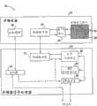
图1是示意性地示出了根据本发明的一个实施方案的用于存储器信号处理的系统20的框图。系统20可用于不同的主机系统和设备中,例如用于计算设备、蜂窝电话或其他通信终端、可移除存储器模块(“U盘”设备)、数码相机、音乐和其他媒体播放器、和/或任何其他存储和取出数据的系统或设备。FIG. 1 is a block diagram schematically illustrating a
系统20包括存储设备24,其将数据存储在存储单元阵列28中。存储阵列28包括多个模拟存储单元32。在本专利申请的上下文中以及在权利要求书中,术语“模拟存储单元”用于描述保持诸如电压或电荷之类的物理参数的连续模拟值的任意的存储单元。阵列28可以包括任何种类的模拟存储单元,举例而言,例如,NAND、NOR和CTF闪存单元、PCM、NROM、FRAM、MRAM和DRAM单元。存储在存储单元中的电荷电平和/或写入与读出存储单元的模拟电压在本文中统称为模拟值。
用于存储在存储设备24中的数据被提供给所述设备并且缓存在数据缓冲器36中。然后所述数据被转换成模拟电压并且使用读/写(R/W)单元40写入存储单元32中,该读/写单元40的功能将在下文中进一步详述。当从阵列28读出数据时,读/写单元40将电荷以及由此的存储单元32的模拟电压转换成数字样本。每个数字样本具有一个或多个比特的分辨率。这些样本被缓存在缓冲器36中。存储设备24的操作和时序均由控制逻辑48所管理。Data for storage in the
数据进出存储设备24的存储和取出,由存储器信号处理器(MSP)52执行。如下文将详示,MSP 52使用新颖的方法,以用于估计和降低在存储单元阵列28中的各种不同的失真效应。The storage and retrieval of data to and from
在一些实施方案中,MSP 52包括编码器/解码器64,该编码器/解码器64使用ECC对将要写到设备24的数据进行编码,而当把数据从设备24读出时对所述ECC进行解码。信号处理单元60处理被写入设备24和从设备24取出的数据。具体地,信号处理单元60估计对从存储单元32读出的电压有影响的失真。信号处理单元60可以补偿抑或减少所估计的失真的效应。替代地,信号处理单元60可以基于所估计的失真而采取其他种类的行动,在下文将详述。In some embodiments, the
MSP 52包括数据缓冲器72,该数据缓冲器72由信号处理单元60用于存储数据以及用于与存储设备24交互。MSP 52还包括输入/输出(I/O)缓冲器56,该输入/输出(I/O)缓冲器56在所述MSP和所述主机之间形成接口。控制器76管理MSP 52的操作和定时。信号处理单元60和控制器76可以用硬件实现。替代地,信号处理单元60和/或控制器76可以包括运行合适的软件的微处理器,或者硬件和软件元素的组合。
图1中的配置是示例性的系统配置,其纯粹是为概念清楚而示出的。也可以使用任意其他合适的配置。为清楚起见,对于理解本发明的原理并非必要的元件,例如各种接口、寻址电路、定时和定序电路、数据置乱电路和调试电路,均从附图中省略。The configuration in FIG. 1 is an exemplary system configuration, which is shown purely for conceptual clarity. Any other suitable configuration may also be used. For clarity, components that are not necessary to understand the principles of the present invention, such as various interfaces, addressing circuits, timing and sequencing circuits, data scrambling circuits and debugging circuits, have been omitted from the drawings.
在图1中所示的示例性系统配置中,存储设备24和MSP 52被实现为两个单独的集成电路(IC)。然而,在替代的实施方案中,所述存储设备和MSP可被集成在单一IC中或片上系统(SoC)中。在一些实施方式中,单个MSP 52可被连接到多个存储设备24。进一步作为替代,MSP 52的某些或全部功能可以用软件实现,并且由主机系统的处理器或其他元件来执行。实现系统20的某些实施方案的另外的架构性的方面,在上文所引用的美国临时专利申请60/867,399中,并且在以援引方式全部纳入本文中的提交于2007年5月10日的题为“CombinedDistortion Estimation and Error Correction Coding for MemoryDevices”的PCT专利申请中,得以更详细地描述。In the exemplary system configuration shown in FIG. 1,
在典型的写操作中,从主机接收待要写入存储设备24的数据,并将所述数据缓存在I/O缓冲器56中。编码器/解码器64编码所述数据,且所编码的数据通过数据缓冲器72传送到存储设备24。在将数据传送到存储设备用于编程之前,MSP 52可以预处理该数据。在设备24中,数据临时存储在缓冲器36中。读/写单元40将数据转换成模拟电压值,并且将数据写入阵列28的适当的存储单元32中。In a typical write operation, data to be written to
在典型的读操作中,读/写单元40从适当的存储单元32读出模拟电压值并且将所述电压转换为软数字样本。所述样本被缓存在缓冲器36中,并且传送到MSP 52的缓冲器72。在一些实施方案中,MSP 52的信号处理单元60将电压样本转换为数据位。如上所述,可能的门限电压的范围被分为两个或更多个区域,其中每个区域表示一个或多个数据位的某一组合。当读取存储单元时,信号处理单元60典型地将读取的电压样本的幅度与一组判决门限相比较,以便确定读取的电压所落入的区域,且从而确定存储在存储单元中的数据位。数据块从缓冲器72传送到信号处理单元60,而编码器/解码器64对这些块的ECC进行解码。已解码的数据通过I/O缓冲器56传送到主机。在一些实施方案中,ECC解码器包括软解码器,而信号处理单元60将电压样本转换成用于解码ECC的软解码度量。In a typical read operation, the read/
另外,信号处理单元60使用下文描述的方法估计在所读取的样本中存在的失真。在一些实施方案中,MSP 52在数据被写入存储单元之前将其置乱,并且将从存储单元读取的数据反置乱,以便改进失真估计的性能。In addition, the
存储阵列结构和失真机制Storage Array Structure and Distortion Mechanism
图2是示意性地示出了根据本发明的一个实施方案的存储单元阵列28的示意图。虽然图2涉及连接在特定阵列配置中的闪存单元,但本发明的原理也可应用于其他类型的存储单元和其他阵列配置。在上文背景技术部分中所引用的参考文献中,描述了一些示例性的存储单元类型和阵列配置。FIG. 2 is a schematic diagram schematically illustrating a
阵列28的存储单元32被布置在具有多个行和多个列的栅格中。每个存储单元32包括浮置栅极金属氧化物半导体(MOS)晶体管。通过向晶体管的栅极、源极和漏极施加适当的电压电平,可以将一定数量的电荷(电子或空穴)存储在一特定的存储单元中。存储在所述存储单元中的值可通过测量所述存储单元的门限电压来读取,所述门限电压被定义为使所述晶体管导通而需要向所述晶体管的栅极施加的最小电压。所读取的门限电压与存储在所述存储单元中的电荷成比例。The
在图2的示例性配置中,每一行中的晶体管的栅极由字线80连接。每一列中的晶体管的源极由位线84连接。在一些实施方案中,例如在一些NOR单元设备中,源极直接连接到位线。在替代的实施方案中,例如在一些NAND单元设备中,位线被连接到多串浮置栅极单元。In the exemplary configuration of FIG. 2 , the gates of the transistors in each row are connected by a word line 80 . The sources of the transistors in each column are connected by bit line 84 . In some implementations, such as in some NOR cell devices, the source is connected directly to the bit line. In alternative implementations, such as in some NAND cell devices, bit lines are connected to strings of floating gate cells.
通常,读/写单元40,通过将变化的电压电平施加到特定的存储单元32的栅极(也即,施加到所述存储单元所连接到的字线),并且检查所述存储单元的漏极电流是否超过了某一门限(也即,所述晶体管是否导通),来读取该特定的存储单元32的门限电压。读/写单元40通常向所述存储单元所连接到的字线施加一系列的不同的电压值,并且确定为使漏极电流超过所述门限的最低栅极电压值。通常,读/写单元40同时读取一整行的存储单元,这一整行的存储单元也被称为页。Typically, read/
在一些实施方案中,读/写单元40通过将所述存储单元的位线预充电到某一电压电平来测量漏极电流。一旦栅极电压被设定到期望值,漏极电流就使得位线电压经存储单元放电。在施加栅极电压之后的几毫秒,读/写单元40测量位线电压,并且将位线电压与门限进行比较。在一些实施方案中,每个位线84被连接到相应的读出放大器,该读出放大器将位线电流放大并且将该电流转换为电压。使用比较器将被放大的电压与门限进行比较。In some implementations, the read/
上文所描述的电压读取方法是一种示例性方法。作为替代,读/写单元40可以使用任何其他适合的方法来用于读取存储单元32的门限电压。例如,读/写单元40可以包括一个或多个模数转换器(ADC),该模数转换器将位线电压转换成数字样本。The voltage reading method described above is an exemplary method. Alternatively, the read/
存储单元阵列通常被分为多个页,也即,多组同时编程和读取的存储单元。在一些实施方案中,每个页包括阵列的一整行。在替代性的实施方案中,每个行可被分为两个或更多个页。对存储单元的擦除通常在包含多个页的块中执行。典型的存储设备可以包括数千个擦除块。尽管也可以使用其它块尺寸,典型的擦除块是128页的数量级,每个擦除块包括数千个存储单元。Arrays of memory cells are typically divided into pages, ie, groups of memory cells that are programmed and read simultaneously. In some implementations, each page includes an entire row of the array. In alternative embodiments, each row may be divided into two or more pages. Erasing of memory cells is typically performed in blocks containing multiple pages. A typical storage device may include thousands of erase blocks. A typical erase block is on the order of 128 pages, each comprising thousands of memory cells, although other block sizes may also be used.
存储在存储单元中的电荷电平和读取自存储单元的电压可能包含多种类型的失真,这些失真是由阵列28中的不同的失真机制所导致的。一些失真机制影响了存储在存储单元中的实际电荷,而其他机制使得所读出的电压失真。例如,阵列中的相邻存储单元之间的电交叉耦合会修改特定存储单元中的门限电压。此效应被称为交叉耦合失真。又例如,电荷会随着时间的推移而从存储单元中泄漏。这种老化效应的结果是,所述存储单元的门限电压将随着时间的推移而从最初写入的值漂移。The charge levels stored in the memory cells and the voltages read from the memory cells may contain various types of distortion caused by different distortion mechanisms in the
另一种类的失真,通常被称为扰动噪声,是由阵列中的某些存储单元上的存储器存取操作(例如,读、写或擦除操作)而导致的,这引起了对其他存储单元中的非预期的电荷改变。作为又一实例,可以由相邻存储单元(例如在同一NAND存储单元串中的其他存储单元)中的电荷,通过一种称为背景图案相关性(BPD)的效应,来影响特定存储单元的源极-漏极电流。Another type of distortion, commonly referred to as disturbance noise, is caused by memory access operations (for example, read, write, or erase operations) on certain memory cells in the array, which cause disturbances to other memory cells. Unexpected charge changes in . As yet another example, the charge in adjacent memory cells (e.g., other memory cells in the same NAND memory cell string) can affect the charge of a particular memory cell through an effect called Background Pattern Dependency (BPD). source-drain current.
失真估计和消除方法Distortion Estimation and Cancellation Methods
存储单元32中的失真降低了存储设备的性能,例如重构数据时的误差概率、可达到的存储容量以及可达到的数据保持期。性能降低在MLC设备中尤其严重,因为在MLC设备中表示数据的不同电压电平之间的差相对较小。在许多情况下,失真度随着时间的推移而变化,且在一个存储单元和另一个存储单元之间也有所不同。从而,以自适应的方式估计失真并且基于所估计的失真采取行动是很有好处的。Distortion in the
MSP 52可以采用各种不同的方法来估计存储单元32中的失真,并且使用所估计的失真度来消除或补偿失真。作为对失真进行补偿的补充或替代,MSP可以基于所估计的失真执行其他种类的动作。The
例如,MSP可以使用所估计的失真来执行数据刷新判决。在一种典型的实现中,MSP估计各个不同的存储单元组(例如存储页)的失真度。当在一特定页中的失真超过某一可容忍的门限时,MSP对数据进行刷新(也即,重新编程)。For example, the MSP can use the estimated distortion to perform data refresh decisions. In a typical implementation, MSP estimates distortion levels for various groups of memory cells (eg, memory pages). When the distortion in a particular page exceeds a certain tolerable threshold, the MSP refreshes (ie, reprograms) the data.
又例如,MSP可以使用所估计的失真来评估在某一存储单元或某组存储单元中的可达到的存储容量。基于可达到的容量,MSP可以修改用于在相应的存储单元中存储数据的电压电平的数量和/或ECC。从而,MSP可以自适应地修改存储单元中存储数据的密度,以匹配它们的存储容量,因为它们的存储容量随着时间的推移而改变。使用失真估计用于适配存储设备的存储密度的一些方面在提交于2007年5月10日的题为“Memory Device with Adaptive Capacity”的PCT专利申请中得以描述,该文献以援引方式全部纳入本文。As another example, the MSP may use the estimated distortion to estimate the achievable storage capacity in a certain storage unit or group of storage units. Based on the achievable capacity, the MSP may modify the number of voltage levels and/or ECC used to store data in the corresponding memory cell. Thus, MSPs can adaptively modify the density of stored data in memory cells to match their storage capacity as their storage capacity changes over time. Some aspects of using distortion estimation for adapting the storage density of a memory device are described in a PCT patent application entitled "Memory Device with Adaptive Capacity," filed May 10, 2007, which is hereby incorporated by reference in its entirety .
再例如,MSP可以基于所估计的失真而修改判决门限,也即将存储单元的可能的电压的范围分成判决区域的门限。MSP可以调整判决门限值以最小化失真度,以最小化解码误差概率或满足任何其他适合的性能条件。MSP也可以修改ECC解码度量,例如对数似然比(LLR),该解码度量由ECC解码器使用以解码ECC。这样的方法例如在上文所引用的PCT申请“Combined Distortion Estimation and ErrorCorrection Coding for Memory Devices”中得以描述。For another example, the MSP may modify the decision threshold based on the estimated distortion, that is, the threshold for dividing the range of possible voltages of the memory cells into decision regions. The MSP may adjust decision thresholds to minimize distortion, to minimize decoding error probability, or to meet any other suitable performance criteria. The MSP can also modify the ECC decoding metric, such as the log-likelihood ratio (LLR), which is used by the ECC decoder to decode the ECC. Such methods are described, for example, in the above-cited PCT application "Combined Distortion Estimation and Error Correction Coding for Memory Devices".
图3至8是示意性地示出了根据本发明的实施方案的用于估计和消除存储单元阵列28中的失真的方法的流程图。在下文的说明中,假设MSP逐页地读取存储单元并估计失真度。然而,在替代性的实施方案中,MSP可以读取并处理任意其他存储单元组。例如,MSP可以处理整个擦除块或甚至单独的存储单元。3 to 8 are flowcharts schematically illustrating a method for estimating and canceling distortion in the
图3是示意性地示出了根据本发明的一个实施方案的一种用于估计和消除交叉耦合失真的方法的流程图。在一些情况下,例如在闪存中,交叉耦合失真是由存储在邻近存储单元的电荷产生的电场的电磁耦合所导致的。在其他情况下,例如在NROM存储单元中,交叉耦合失真可由其他原因导致,例如由于共享地线导致的存储单元的源电压的上升。FIG. 3 is a flowchart schematically illustrating a method for estimating and eliminating cross-coupling distortion according to an embodiment of the present invention. In some cases, such as in flash memory, cross-coupling distortion is caused by electromagnetic coupling of electric fields generated by charges stored in adjacent memory cells. In other cases, such as in NROM memory cells, cross-coupling distortion may be caused by other causes, such as a rise in the source voltage of the memory cell due to a shared ground line.
读取自受交叉耦合影响的某一存储单元i的电压一般可写为:The voltage read from a certain memory cell i affected by cross-coupling can generally be written as:
[1] vi=g(ci)+f(ci,Ci)[1] vi =g(ci )+f(ci ,Ci )
其中g(ci)表示当所有潜在干扰存储单元均被擦除时从所述存储单元读取的电压,ci表示在存储单元i中的电荷电平,f(ci,Ci)表示当存储单元电荷是ci时的耦合效应,而Ci表示相邻存储单元的电荷电平的集合,j≠i。where g(ci) represents the voltage read from the memory cell when all potentially interfering memory cells are erased,ci represents the charge level in memory cell i, and f(ci ,Ci ) represents The coupling effect when the storage cell charge is ci , and Ci represents the set of charge levels of adjacent storage cells, j≠i.
在一些实际情况下,交叉耦合可以用线性函数来建模,以使得In some practical cases, the cross-coupling can be modeled by a linear function such that
[2]
其中kji表示交叉耦合系数,也即,从存储单元j到存储单元i的交叉耦合幅度。系数值有时可以取决于存储单元的电荷电平。where kji represents the cross-coupling coefficient, that is, the magnitude of the cross-coupling from memory cell j to memory cell i. The coefficient value can sometimes depend on the charge level of the memory cell.
在其他情况下,由某一干扰存储单元导致的交叉耦合既取决于干扰存储单元的电荷电平,也取决于被干扰存储单元的电荷电平。在这些情况下,公式[2]可被写为In other cases, the cross-coupling caused by a disturbing memory cell depends on both the charge level of the disturbing memory cell and the charge level of the disturbed memory cell. In these cases, formula [2] can be written as
[3] vi=k0·ci+f({ci,cj},j≠i)[3] vi =k0 ·ci +f({ci , cj }, j≠i)
交叉耦合系数值通常可以从一个单元到另一个单元而变化,也可以随着温度、电源电压和其他条件的变化而变化。Cross-coupling coefficient values can often vary from one unit to another, as well as with changes in temperature, supply voltage, and other conditions.
在读取步骤90,图3的方法始于MSP52从一存储单元页读取电压。每个读取电压由软样本所表示,也即具有两个或更多个位的分辨率的数字化值。所述MSP从读取的电压值生成硬判决。换句话说,所述MSP逐个存储单元确定最有可能已被写到存储单元中的标称电压电平。MSP可以将每个读取电压和表示不同比特组合的不同标称电压值作比较,并且确定最接近于读取电压的标称电压电平。这种操作通常称为硬分割。In a
在系数估计步骤94,MSP基于读取的电压样本并基于对应的硬判决,估计交叉耦合系数。在大多数实际情况下,大多数硬判决反映了写入存储单元的正确比特组合,只有很少的硬判决是错误的。虽然硬判决的错误概率不足以用于可靠地重构数据,但其通常足以用于可靠地估计系数。In a
MSP可以使用任何适当的估计方法用于估计交叉耦合系数的值。在许多实际情况下,耦合系数值在整个已处理的存储单元组中基本恒定。在这些情况下,MSP可以使用本领域公知的各种不同的块估计技术,这些块估计技术使用软电压样本的整个集合和对应的硬判决来估计交叉耦合系数。MSP may use any suitable estimation method for estimating the value of the cross-coupling coefficient. In many practical cases, the coupling coefficient value is substantially constant throughout the processed bank group. In these cases, the MSP can use various block estimation techniques known in the art that use the entire set of soft voltage samples and corresponding hard decisions to estimate the cross-coupling coefficients.
替代地,所述MSP可以使用本领域公知的各种不同的循序估计方法,其循序地(例如逐个样本地)处理电压样本和硬判决,并且收敛成交叉耦合系数的期望值。循序估计方法可以包括,例如最小均方(LMS)过程、递归最小二乘(RLS)过程、Kalman过滤过程或者任何其他适合的过程。Alternatively, the MSP may use various sequential estimation methods known in the art that process voltage samples and hard decisions sequentially (eg, sample-by-sample) and converge to expected values for the cross-coupling coefficients. Sequential estimation methods may include, for example, a Least Mean Square (LMS) process, a Recursive Least Squares (RLS) process, a Kalman filtering process, or any other suitable process.
在一些实施方案下,估计过程试图减少在读取电压和对应的硬判决之间的距离度量(例如欧几里得距离)。Under some embodiments, the estimation process attempts to reduce a distance metric (eg, Euclidean distance) between read voltages and corresponding hard decisions.
例如,当使用LMS过程时,MSP可以迭代地估算下述表达式For example, when using an LMS process, MSP can iteratively evaluate the following expression
[4]
其中t表示根据已处理的样本和硬判决而递增的增量指数(例如,样本指数)。


在一些实施方案中,在对存储单元编程期间,可以通过测量由对存储单元j编程而在存储单元电压vi中导致的变化,来估计kji的值。In some embodiments, during programming of a memory cell, the value of kji can be estimated by measuring the change in memory cell voltagevi caused by programming memory cell j.
在交叉耦合补偿步骤98,MSP基于所估计的交叉耦合系数补偿读取电压中的交叉耦合失真。MSP通常产生校正的电压,其中交叉耦合失真度被降低。例如,MSP可以将所估计的交叉耦合失真分量求和,并且从存储单元电压中减去该和,所述交叉耦合失真分量源自不同的干扰存储单元并且影响某一读取电压。这种操作有时称为线性均衡。In a
如本领域所公知,MSP可以替代地通过施加判决反馈均衡(DFE)来消除交叉耦合失真。在替代性的实施方案中,所述MSP可以使用减少状态最大似然序列估计(MLSE)过程,例如使用众所周知的Viterbi算法,来消除交叉耦合失真。此外作为替代,所述MSP可以使用最大后验(MAP)估计过程或任何其他适合的方法以基于所估计的交叉耦合系数来补偿交叉耦合失真。As is known in the art, MSP can instead cancel cross-coupling distortion by applying decision feedback equalization (DFE). In an alternative embodiment, the MSP may use a reduced-state Maximum Likelihood Sequence Estimation (MLSE) procedure, such as using the well-known Viterbi algorithm, to remove cross-coupling distortions. Also alternatively, the MSP may use a Maximum A Posteriori (MAP) estimation procedure or any other suitable method to compensate for cross-coupling distortions based on estimated cross-coupling coefficients.
所述MSP使用校正的电压来重构存储单元中存储的数据。在一些实施方案中,所述MSP分两步处理读取的电压(也即,两次扫描读取的电压值)。在第一步,MSP估计交叉耦合系数。在第二步,MSP使用所估计的系数来校正读取电压并且重构数据。两步处理可以是有利的,举例而言,例如由于在不同温度、电源电压或其他条件下写存储单元,而存储单元的不同的块或页具有不同的交叉耦合系数值时。在替代性的实施方案中,MSP可以在一步之内执行系数估计、失真补偿和数据重构。The MSP uses the corrected voltage to reconstruct data stored in the memory cell. In some embodiments, the MSP processes the voltage reads in two steps (ie, scans the voltage reads twice). In the first step, MSP estimates the cross-coupling coefficients. In a second step, the MSP uses the estimated coefficients to correct the read voltage and reconstruct the data. A two-step process may be advantageous, for example, when different blocks or pages of memory cells have different cross-coupling coefficient values, such as due to writing the memory cells at different temperatures, supply voltages, or other conditions. In an alternative embodiment, MSP can perform coefficient estimation, distortion compensation and data reconstruction in one step.
在一个替代性的实施方案中,MSP起初在一步之内执行系数估计和数据重构。然后MSP估计重构的数据的质量(例如通过检测未被ECC校正的错误),并且若数据重构质量过低则执行第二步。这种技术不会显著地改变平均的处理时延或处理功率,在系数随着时间的推移而改变的情况下是有利的。In an alternative embodiment, MSP initially performs coefficient estimation and data reconstruction in one step. The MSP then estimates the quality of the reconstructed data (eg by detecting errors not corrected by ECC), and performs a second step if the quality of the data reconstruction is too low. This technique does not significantly change the average processing latency or processing power, which is advantageous where the coefficients change over time.
如上所述,在一些实施方案中,MSP在将数据写到存储单元之前将数据置乱,以便防止非随机数据使估计精确度降低。As noted above, in some embodiments, the MSP scrambles the data before writing it to the memory cells in order to prevent non-random data from degrading the estimation accuracy.
在一些失真机制中,特定存储单元中的失真度和沿同一位线而处的其他存储单元的失真度是相关的。例如,在一些NAND闪存中,沿着每条位线的存储单元彼此相连构成十六个或三十二个存储单元组成的组,称为串。读取自特定存储单元的电压通常取决于串中的其他存储单元的电压。此效应通常称为背景图案相关性(BPD)。又例如,由读出放大器导致的参数变化和其他失真也可以在沿着一条位线的不同存储单元中相关联。In some distortion mechanisms, the degree of distortion in a particular memory cell is related to the degree of distortion in other memory cells located along the same bit line. For example, in some NAND flash memories, memory cells along each bit line are connected to each other to form groups of sixteen or thirty-two memory cells, called strings. The voltage read from a particular memory cell typically depends on the voltages of other memory cells in the string. This effect is often referred to as Background Pattern Dependency (BPD). As another example, parameter variations and other distortions caused by sense amplifiers can also be correlated among different memory cells along a bit line.
在其他情况下,具体存储单元中的失真度可以和沿同一字线而处的其他存储单元的失真度相关联。例如,考虑和同一页中的其他存储单元相比需要明显更长的编程时间的某一存储单元。当所涉及的页正在被编程时,在一定次数的P&V迭代之后,大多数存储单元达到它们的预期电荷电平,但是在“慢”存储单元中的电荷电平仍然远不达期望电平。因此,在慢存储单元中的源极-漏极电流就因此而较低。使用另外的P&V迭代过程继续对该慢存储单元进行编程,而其电流增大。增大的电流增大了落在地线上的电压以及页中其他存储单元的源极-漏极电压。作为结果,页中的其他存储单元的门限电压下降。In other cases, the degree of distortion in a particular memory cell may be correlated with the degree of distortion in other memory cells located along the same word line. For example, consider a certain memory cell that requires a significantly longer programming time than other memory cells in the same page. When the page in question is being programmed, after a certain number of P&V iterations, most memory cells reach their expected charge level, but the charge level in the "slow" memory cells is still far from the desired level. Therefore, the source-drain current in the slow memory cell is therefore lower. The slow memory cell continues to be programmed using additional P&V iterations while its current is increased. The increased current increases the voltage falling on ground and the source-drain voltages of other memory cells in the page. As a result, the threshold voltages of other memory cells in the page drop.
虽然下文对图4的说明涉及沿着位线的相关失真,然而图4的方法也可以用于预测和补偿沿着字线的相关失真。此外作为替代,所述方法可被用于预测和校正任何其他在某一组中的存储单元的失真度彼此相关的失真机制,这样的存储单元例如为在阵列中彼此极为接近的存储单元,以及具有相同电源电压(Vcc)线、地线或功率供应电路的存储单元。Although the following description of FIG. 4 refers to relative distortion along bit lines, the method of FIG. 4 can also be used to predict and compensate relative distortion along word lines. Also as an alternative, the method can be used to predict and correct for any other distortion mechanism in which the degrees of distortion of memory cells in a certain group are related to each other, such memory cells being in close proximity to each other in an array, for example, and Memory cells with the same supply voltage (Vcc) line, ground line or power supply circuit.
当沿着某一位线的存储单元的失真度相关时,有时可将失真度建模为When the degree of distortion of memory cells along a bit line is related, the degree of distortion can sometimes be modeled as
[5]
其中e(n,m)表示在列(位线)m和行(页)n处的存储单元的失真度。c(i,m)表示从第i页的第m位线处的存储单元读取的电压。fi和gi分别表示定义在第i页的一个存储单元的电压与沿着同一位线在先前页中和后继页中的存储单元的依赖关系的函数。公式[5]假设页被循序处理。where e(n,m) represents the degree of distortion of the memory cell at column (bit line) m and row (page) n. c(i,m) represents the voltage read from the memory cell at the m-th bit line of the i-th page. fi andgi denote functions of the dependence of the voltage of a memory cell defined in page i on the memory cells in the previous page and in the succeeding page along the same bit line, respectively. Equation [5] assumes that pages are processed sequentially.
图4是示意性地示出了根据本发明的一个实施方案的用于预测和消除位线相关失真的一种迭代方法的流程图。在失真记录步骤102,所述方法始于MSP记录先前读取的存储单元的失真度。可能在ECC解码之后,MSP可以用任何适当的方法计算失真度,例如通过将读取电压与期望的标称电压相比较。Figure 4 is a flow diagram schematically illustrating an iterative method for predicting and canceling bit line related distortion according to one embodiment of the present invention. In a
在目标读取步骤106,MSP读取特定存储单元的电压,这个存储单元被称为目标存储单元。然后在预测步骤110,MSP基于记录的沿同一位线的其他存储单元的失真度值,并基于从这些存储单元读取的电压,预测在目标存储单元之中的失真度。例如,MSP可以使用上述公式[5]预测失真度。In a target read
在校正步骤114,MSP使用所估计的失真度来校正从目标存储单元读取的电压.然后在解码步骤118,MSP基于校正的电压,对存储在目标存储单元中的数据进行解码。当ECC解码器包括软解码器时,MSP可以替代地基于所估计的失真度,校正存储在存储单元中的比特的软ECC度量(例如,LLR)。此类校正办法,例如在上述PCT申请“CombinedDistortion Estimation and Error Correction Coding for MemoryDevices”中得以描述。In a
虽然图4的描述为清楚起见注重于单个目标存储单元,但是随着从存储器读取页,预测和校正过程通常并行地在多个存储单元中执行。While the description of FIG. 4 focuses on a single target memory cell for clarity, the predictive and corrective processes are typically performed in parallel across multiple memory cells as pages are read from memory.
为了改进存储效率,MSP可以仅为每个位线存储单个失真值,而不是记录并存储每个先前读取的存储单元的失真度。存储的值,标注为ê(m),表示在读取第n页之后的e(n,m)的估计值。对于读取的第一页,ê(m)通常被初始化为0。To improve storage efficiency, the MSP may only store a single distortion value for each bit line, rather than recording and storing the distortion level for each previously read memory cell. The stored value, denoted ê(m), represents the estimated value of e(n,m) after reading the nth page. For the first page read, ê(m) is usually initialized to 0.
当对第n页解码时,MSP更新ê(m)的值,例如使用表达式When decoding page n, MSP updates the value of ê(m), for example using the expression
[6]
其中δn表示用于第n页的预定步长。c(n,m)表示从第n页的第m位线的存储单元读取的电压,而表示该存储单元的基于解码器输出的标称电压。当读取第n+1页时,MSP可以通过估算ê(m)=ê(m)-fn+1·c(n+1,m)+gn·c(n,m)来基于ê(m)预测失真。校正电压(例如,c(n+1,m)-ê(m))被用来解码数据。where δn denotes the predetermined step size for the nth page. c(n,m) represents the voltage read from the memory cell of the mth bit line of the nth page, and Indicates the nominal voltage of this memory cell based on the decoder output. When reading page n+1, MSP can estimate ê(m)=ê(m)-fn+1 c(n+1,m)+gn c(n,m) based on ê (m) Prediction Distortion. A correction voltage (eg, c(n+1,m)-ê(m)) is used to decode the data.
上述方法在预测和校正读出放大器的变化的增益、偏差或其他变化的参数时会尤其有效。此类参数还可以包括对特定电压电平的分布或所有电压电平的联合分布的可变的偏差或展宽。The method described above can be particularly effective in predicting and correcting for varying gain, offset, or other varying parameters of a sense amplifier. Such parameters may also include a variable deviation or broadening of the distribution of a particular voltage level or the joint distribution of all voltage levels.
当此方法用于校正NAND闪存存储单元阵列中的BPD失真时,可能存在一个贡献了大部分失真的特定单元,例如因为它被过编程。在这种情况下,迭代方法可以在NAND存储单元上重复,直到这个存储单元被识别,在这时刻ê(m)的值被重置。不同于通常在每个NAND存储单元串执行的对BPD失真的校正,通常是在每条完整位线上追踪和执行读出放大器的变化。When this method is used to correct BPD distortion in an array of NAND flash memory cells, there may be one particular cell that contributes most of the distortion, for example because it is overprogrammed. In this case, the iterative method can be repeated on the NAND memory cell until this memory cell is identified, at which point the value of ê(m) is reset. Unlike the correction for BPD distortion that is typically performed on each NAND memory cell string, the sense amplifier changes are typically tracked and performed on each full bit line.
在一些实施方案中,MSP52维持保持每条位线、字线或其他相关存储单元组的所追踪的参数的表格或其他数据结构。In some implementations,
如上所述,一些存储单元可能受扰动噪声影响,扰动噪声也就是由阵列中的其他存储单元上执行的操作所导致的失真。在一些实施方案中,MSP52校正扰动噪声是在形成扰动噪声之时,而不是在读取被干扰存储单元时。As noted above, some memory cells may be affected by disturbance noise, which is distortion caused by operations performed on other memory cells in the array. In some embodiments, the
图5是示意性地示出了根据本发明的一个实施方案的一种用于校正扰动噪声的方法的流程图。在扰动创建操作步骤122,所述方法始于MSP52执行存储器存取操作,该存储器存取操作可对一些存储单元贡献扰动噪声。存储器存取操作可以包括,例如,编程、读或擦除操作。在读取潜在被扰动存储单元的步骤126,MSP从可能被存储器存取操作所扰动的存储单元读取电压。FIG. 5 is a flowchart schematically illustrating a method for correcting disturbance noise according to an embodiment of the present invention. At a disturbance creation operation step 122, the method begins with the
在扰动估计步骤130,MSP评估在潜在被扰动存储单元中的扰动噪声的电平。为此目的,MSP可以使用任何适合的失真估计方法。例如,所述MSP可以使用判决导向方法,其中将读取自存储单元的电压和由硬分割所确定的相应标称电压电平相比较,或者与通过将ECC解码运用于读取自存储单元的电压而确定的标称电压电平作比较。In a disturbance estimation step 130, the MSP evaluates the level of disturbance noise in the potentially disturbed memory cells. For this purpose, MSP may use any suitable distortion estimation method. For example, the MSP may use a decision-directed approach where the voltage read from a memory cell is compared to the corresponding nominal voltage level determined by hard segmentation, or to the voltage read from the memory cell by applying ECC decoding to The nominal voltage level determined by the voltage is compared.
在一些情况下,扰动噪声可以增加在相邻页中的一些已擦除存储单元中的电荷电平。在这样的情况下,MSP可以通过对潜在被扰动页中的已擦除存储单元(也即,其电压低于某一门限电平的存储单元,该门限电平可以不同于通常用于检测已擦除存储单元的门限电平)的数量进行计数,来评估扰动电平。MSP可以将潜在扰动存储器存取操作之前和之后的已擦除存储单元的数量进行比较,并且从这两个结果之间的差来评估扰动电平。In some cases, disturbance noise can increase the charge level in some erased memory cells in adjacent pages. In such cases, the MSP may pass through the potentially disturbed page to erased memory cells (i.e., memory cells whose voltage is below a certain threshold level, which may differ from the The number of detected threshold levels of erased memory cells) is counted to evaluate the disturbance level. The MSP can compare the number of erased memory cells before and after a potentially disturbing memory access operation and estimate the disturbance level from the difference between these two results.
在高扰动检查步骤134,MSP检查所估计的失真度是否超过一预定义的门限。在扰动校正步骤138,如果扰动电平被视为高,则MSP校正在潜在被扰动存储单元中的扰动噪声。例如,MSP可以刷新在同一存储单元中的数据,重新编程在其他存储单元中(也即,在另一页中)的数据,或对现有的已编程的存储单元增加电荷。MSP也可以使用更强的ECC来编码数据,并且将新编码的数据存储在另一页中。否则,也即,如果扰动电平被认为可容忍,则在终止步骤142终止该方法。In a high disturbance check step 134, the MSP checks whether the estimated distortion level exceeds a predefined threshold. In a disturbance correction step 138, if the disturbance level is deemed high, the MSP corrects the disturbance noise in the potentially disturbed memory cell. For example, the MSP can refresh data in the same memory cell, reprogram data in other memory cells (ie, in another page), or add charge to an existing programmed memory cell. MSP can also use stronger ECC to encode data, and store the newly encoded data in another page. Otherwise, that is, if the disturbance level is considered tolerable, the method is terminated at a termination step 142 .
在一些情况下,在每次读、写和擦除操作之后执行图5的方法,会显著地增加处理时间。因此,在一些实施方案中,MSP仅仅在系统空闲的时间段期间执行图5的方法。In some cases, performing the method of FIG. 5 after each read, write, and erase operation can significantly increase processing time. Thus, in some embodiments, the MSP only performs the method of FIG. 5 during periods when the system is idle.
图6是根据本发明的一个替代性的实施方案,示意性地示出了用于校正扰动噪声的另一种方法的流程图。所述方法基于扰动噪声是由比目标存储单元更新近地编程的存储单元贡献到该目标存储单元的事实。为简洁起见,比目标存储单元更为新近地编程的存储单元被称为与目标单元相比“较年轻”。比目标存储单元更早编程的存储单元被称为“较老”存储单元。Fig. 6 is a flowchart schematically illustrating another method for correcting disturbance noise according to an alternative embodiment of the present invention. The method is based on the fact that disturbance noise is contributed to the target memory cell by memory cells programmed more recently than the target memory cell. For brevity, memory cells that are more recently programmed than the target memory cell are said to be "younger" than the target cell. Memory cells programmed earlier than the target memory cell are referred to as "older" memory cells.
在潜在干扰存储单元识别步骤146,上述方法始于MSP 52识别潜在地对目标存储单元引发扰动噪声的存储单元。在较年轻存储单元识别步骤150,MSP识别并标记哪些潜在干扰存储单元比目标存储单元较年轻。在一些实施方案中,MSP存储每个页被编程的时间标记,其通常作为页的一部分和数据一起存储。所述MSP查询所存储的标记,以便确定哪些存储单元比目标存储单元较年轻。In a potentially disturbing memory
当循序写存储器页时,MSP可以把在较大编号的页中的存储单元视为相比目标单元较年轻。替代地,当未循序写存储器页时,MSP可以在每个页中存储一个变量,该变量指示该页与相邻页相比的相对年龄。当此页被编程时,上述变量被设置并存储。例如,所述变量可以包括如下计数值,其对迄今为止在擦除块中被编程的页的数量进行计数。替代地,上述变量可以为每个相邻页包含一个布尔标志,其指示在当前页被编程时,相邻页是已编程还是已擦除。此外作为替代,MSP可以使用任何其他适合的方法以确定与目标存储单元相比较年轻的潜在干扰存储单元。When writing memory pages sequentially, the MSP may consider memory cells in higher numbered pages to be younger than the target cells. Alternatively, when pages of memory are not written sequentially, the MSP can store a variable in each page that indicates the relative age of that page compared to adjacent pages. When this page is programmed, the above variables are set and stored. For example, the variable may include a count value that counts the number of pages programmed so far in the erase block. Alternatively, the variables described above may contain a Boolean flag for each adjacent page that indicates whether the adjacent page was programmed or erased when the current page was programmed. Also alternatively, the MSP may use any other suitable method to determine potentially interfering memory cells that are younger than the target memory cell.
在干扰存储单元读取步骤154,MSP52读取被标记的存储单元(也即,比目标存储单元较年轻的潜在干扰存储单元)的电压。所述MSP可以重新读取干扰存储单元和/或使用ECC解码器对存储在潜在干扰存储单元中的数据进行可靠地解码。在目标存储单元读取步骤158,所述MSP也读取目标存储单元的电压。在一些实施方案中,目标存储单元的电压以高分辨率读取,例如使用具有位数高于存储在每个存储单元中的数据位数的ADC。被标记的存储单元的电压有时可以用降低的分辨率读取。In a disturbed memory cell read
在扰动贡献估计步骤162,所述MSP估计由较年轻潜在干扰存储单元贡献到目标存储单元的扰动噪声的电平。所估计的扰动电平可以取决于:潜在被干扰存储单元的相对年龄、存储在潜在干扰存储单元中的电压值和/或数据、潜在干扰存储单元相对于目标存储单元的位置(例如,它们是否位于一相邻页、第二相邻页,等等)、被干扰存储单元的最近的编程-擦除循环的次数和/或其他信息或判据。对扰动电平的一种有效估计,是该扰动电平以上述参数为条件的平均值。In a disturbance
在扰动消除步骤166,所述MSP对所估计的扰动电平进行补偿。例如,所述MSP可以从读取自目标存储单元的电压中减去所估计的扰动电平,以产生校正的电压。校正的电压被用于对存储在目标存储单元中的数据解码,或者用于修改ECC解码器度量。In a
虽然上述说明为清楚起见注重于单个目标存储单元,但是图6的过程也可以随着从存储器读取页,而并行地针对多个目标存储单元执行。Although the above description focuses on a single target memory unit for clarity, the process of FIG. 6 may also be performed in parallel for multiple target memory units as pages are read from memory.
在一些实施方案中,使用编程与验证(P&V)过程对存储单元编程,而当对存储单元编程时,MSP52采用失真补偿。在一些实施方案中,MSP在对存储单元的编程和读取期间均采用失真补偿。In some implementations, the memory cells are programmed using a program and verify (P&V) process, and the
P&V过程通常用于对存储单元编程。在一典型的P&V过程,通过施加一系列电压脉冲而对一存储单元编程,该一系列电压脉冲的电压电平逐个脉冲增加。在每个脉冲之后,读取(“验证”)已编程的电压电平,且迭代继续进行直到达到期望的电平。P&V过程,例如,由Jung等人于1996年11月在IEEE Journal of Solid State Circuits(11:31)的1575页-1583页上发表的“A117mm2 3.3V Only 128Mb MultilevelNAND Flash Memory for Mass Storage Applications”中描述,以及由Lee等人于2002年5月在IEEE Electron Device Letters(23:5)的264页-266页发表的“Effects of Floating Gate Interference onNAND Flash Memory Cell Operation”中描述,上述文献均在此处以援引方式纳入本文。The P&V process is typically used to program memory cells. In a typical P&V process, a memory cell is programmed by applying a series of voltage pulses whose voltage level increases pulse by pulse. After each pulse, the programmed voltage level is read ("verified") and the iterations continue until the desired level is reached. P&V process, for example, "A117mm2 3.3V Only 128Mb MultilevelNAND Flash Memory for Mass Storage Applications" by Jung et al., IEEE Journal of Solid State Circuits (11:31), pp. 1575-1583, Nov. 1996 Described in, and described in "Effects of Floating Gate Interference onNAND Flash Memory Cell Operation" published by Lee et al. in May 2002 on pages 264-266 of IEEE Electron Device Letters (23:5), the above-mentioned documents are all in It is hereby incorporated by reference.
图7是示意性地示出了根据本发明的另一实施方案的用于在存储单元阵列28之中估计和消除失真的方法的流程图。与一些已知的验证读取自存储单元的电压达到期望值的P&V过程不同,图7的方法使得存储在存储单元中的电荷达到期望的电荷,这个电荷表示所存储的数据。FIG. 7 is a flowchart schematically illustrating a method for estimating and canceling distortion in the
验证存储在存储单元中的电荷电平而不是读取电压,是有好处的,因为在写时和读时的失真度可能是不同的。此方法可以用于补偿任何失真类型或者机制。It is beneficial to verify the charge level stored in the memory cell rather than the read voltage, because the degree of distortion may be different during writing and reading. This method can be used to compensate for any distortion type or mechanism.
所述方法始于MSP52意欲对某页编程之时。在潜在干扰存储单元读取步骤170,对于页中一将要编程的给定目标存储单元,MSP读取潜在地导致该目标存储单元失真的存储单元。(在一些情况下,MSP已经处理了这些值,因为它们刚被编程,在这种情况下没有必要读取这些存储单元。)在失真计算步骤174,所述MSP估计由潜在干扰存储单元导致的对目标存储单元的失真。所述MSP可以使用任何适当的方法,例如上述的各种不同的估计过程,用于估计失真度。The method starts when the MSP52 intends to program a page. In a potentially disturbing memory cell read
基于所估计的失真,MSP计算一预先校正的电压值以便编程目标存储单元。通常,MSP通过从意图在所述存储单元中存储的标称电压电平中减去所估计的失真度,来产生校正的电压。Based on the estimated distortion, the MSP calculates a pre-corrected voltage value for programming the target memory cell. Typically, the MSP generates a corrected voltage by subtracting the estimated degree of distortion from the nominal voltage level intended to be stored in the memory cell.
在预校正编程步骤178,所述MSP使用P&V过程,以预校正的电压对目标存储单元编程。作为结果,存储在目标存储单元中的电荷电平真实地反映了写到存储单元中的数据,因为它被预先校正以移除在写的时候存在的失真。In a
在存储单元读取步骤182,对存储单元的读取可能在对该存储单元编程之后很久才发生,当读取存储单元时,MSP读取目标存储单元以及潜在干扰存储单元。在失真重新估计步骤186,MSP重新估计在读取时由潜在干扰存储单元对目标存储单元导致的失真。MSP可以使用任何适合的方法,例如上述的各种不同的估计过程,用于重新估计所述失真度。In the memory cell read
如上所述,目标存储单元可能在很久以前已被编程,而诸如温度和电源电压之类的操作条件可能已经改变。此外,在目标存储单元被编程之后,另外的潜在干扰存储单元可能已经被读、编程或擦除。从而,在步骤186计算的失真度可能与在上述步骤174计算的失真度大相径庭。As mentioned above, the target memory cell may have been programmed a long time ago, and operating conditions such as temperature and supply voltage may have changed. Additionally, additional potentially disturbing memory cells may have been read, programmed, or erased after the target memory cell was programmed. Thus, the distortion measure calculated at
在校正步骤190,MSP基于重新估计的失真,校正读取自目标存储单元的电压。校正的电压被用于解码自目标存储单元的数据。为了在读取干扰存储单元的电压时减少失真,以判决导向方式迭代地执行对存储单元数据的解码。In a
在图7的方法中,在写存储单元的时候和读存储单元的时候都校正失真,且每次校正均使用当前存在的实际失真度。从而,相对于已知的P&V过程,本方法更具鲁棒性,并且更容忍对操作条件和随后的编程操作进行的改变。In the method of FIG. 7, the distortion is corrected both when writing the memory cell and when reading the memory cell, and each correction uses the actual degree of distortion currently existing. Thus, the method is more robust and more tolerant to changes in operating conditions and subsequent programming operations relative to known P&V procedures.
在一些实施方案中,仅仅在编程期间采用失真校正,且不经过二次失真校正即对存储单元进行读取。在这些实施方案中,图7的方法的步骤182至190被略去,而MSP应该将来自未经编程的存储单元的干扰纳入考虑。In some implementations, distortion correction is employed only during programming, and memory cells are read without secondary distortion correction. In these embodiments,
图8是示意性地示出了根据本发明的一个实施方案用于估计目标存储单元中的失真的又一种方法的流程图。图8的方法利用如下事实,即由在目标存储单元之前编程的存储单元导致的失真可不同于在目标存储单元之后编程的存储单元导致的失真。FIG. 8 is a flowchart schematically illustrating yet another method for estimating distortion in a target storage unit according to an embodiment of the present invention. The method of FIG. 8 takes advantage of the fact that the distortion caused by memory cells programmed before the target memory cell can be different than the distortion caused by memory cells programmed after the target memory cell.
另一种假设是,所述阵列使用P&V过程编程,如上所述。在一些已知的P&V过程中,例如在上文引用的由Jung等人所著的文献中,在某一页中的每个存储单元都被编程为标注以0至M-1的M个电压电平中的一个,其中电平0是已擦除电平。所述P&V过程分M个阶段对所述页编程。在阶段i,一系列电压脉冲被施加到编程电平应该为i或更高的存储单元。在每个脉冲之后,所述过程读取不同存储单元的电压,并且停止向已经达到其期望电平的存储单元施加脉冲。Another assumption is that the array is programmed using a P&V process, as described above. In some known P&V processes, such as in Jung et al. cited above, each memory cell in a certain page is programmed with M voltages labeled 0 to M-1 One of the levels, where level 0 is the erased level. The P&V process programs the page in M stages. In phase i, a series of voltage pulses are applied to memory cells whose programming level should be i or higher. After each pulse, the process reads the voltage of a different memory cell and stops applying pulses to memory cells that have reached their desired level.
在一些实施方案中,对于一给定的目标存储单元,MSP根据编程时间对潜在干扰存储单元分类。(如上所述,MSP可以存储每个页的被编程的时间标记,并且将存储的标记用于分类过程。)存储单元的一子集,标注为D1,包括潜在干扰存储单元,其在目标存储单元被编程时并未被所述P&V过程完全编程。当目标存储单元被编程时,类D1中的存储单元处于已擦除电平或是被部分编程,但是可能从那时起已被编程。In some embodiments, for a given target memory cell, the MSP classifies potentially disturbing memory cells according to programming time. (As mentioned above, the MSP can store the programmed time stamp for each page and use the stored stamp for the sorting process.) A subset of memory cells, labeled D1, includes potentially disturbing memory cells that are in the target memory Cells are not fully programmed by the P&V process when they are programmed. The memory cells in class D1 were at the erased level or were partially programmed when the target memory cell was programmed, but may have been programmed since then.
在一些编程方案中,分数个阶段对存储单元编程。例如,在一些4电平存储单元编程方法中,最低有效位(LSB)和最高有效位(MSB)被在两个单独的步骤中写入。一种示例性的方法由Takeuchi等人于1998年8月在IEEE Journal of Solid-State Circuits(33:8)的1228页-1238页发表的“A Multipage Cell Architecture for High-SpeedProgramming Multilevel NAND Flash Memories”中描述,该文献在此处以援引方式纳入本文。在此类方法中,在某一时间点可将存储单元编程到中间电平,而未来编程步骤将所述存储单元编程到其最终编程值。当使用此类编程方法时,类D1被扩展而包括如下存储单元,该存储单元在目标存储单元被编程时处于已擦除电平或处于中间编程电平,但可以自那时起编程到其最终值。In some programming schemes, memory cells are programmed in fractional stages. For example, in some 4-level memory cell programming methods, the least significant bit (LSB) and the most significant bit (MSB) are written in two separate steps. An exemplary method is "A Multipage Cell Architecture for High-Speed Programming Multilevel NAND Flash Memories" published by Takeuchi et al. on pages 1228-1238 of IEEE Journal of Solid-State Circuits (33:8) in August, 1998 described in , which is hereby incorporated by reference. In such methods, a memory cell may be programmed to an intermediate level at some point in time, while a future programming step programs the memory cell to its final programmed value. When this type of programming method is used, class D1 is extended to include memory cells that were either at an erased level or at an intermediate programming level when the target memory cell was programmed, but can be programmed to its other level since then. final value.
存储单元32的另一子集,标注为D2,包括潜在干扰存储单元,其在目标存储单元被编程时已被编程。因为当目标存储单元被编程时,从这些存储单元到该目标存储单元的干扰已经存在,故所述P&V过程已经至少部分地对此干扰进行补偿。第三类存储单元,标注为D3,包括与所述目标存储单元并发编程的潜在干扰存储单元,例如,与所述目标存储单元处于同一页上的存储单元。Another subset of
MSP52可以根据不同类的潜在干扰存储单元,估计针对目标存储单元的失真。设n和m各自表示阵列28中目标存储单元的行号和列号。则xn,m表示在使用所述P&V过程写目标存储单元之后此目标存储单元的电压。xi,j表示在上次编程迭代之后的目标存储单元电压被验证时的位于i行和j列的存储单元的电压。yn,m表示读取自目标存储单元的存储单元电压值,由于失真,它不同于xn,m。MSP52 can estimate the distortion for a target memory cell based on different types of potentially interfering memory cells. Let n and m denote the row number and column number of the target memory cell in
在yn,m中存在的总失真可被写为The total distortion present in yn,m can be written as
[7]
其中hn,m,i,j表示从位于i行j列的干扰存储单元到位于n行m列的目标存储单元的交叉耦合干扰系数。b表示常数偏项。虽然上述公式[7]涉及线性失真模型,但也可以使用非线性模型。Where hn, m, i, j represent the cross-coupling interference coefficients from the interfering storage unit located in row i and column j to the target storage unit located in row n and column m. b represents a constant partial term. While the above formula [7] refers to a linear distortion model, non-linear models can also be used.
类D1中的存储单元包括在目标存储单元被编程之后而被编程的存储单元。因此,由于该编程操作而添加到这些存储单元的电荷所导致的干扰在那时并不存在,并且所述P&V过程也不可能已经对此失真做补偿。The memory cells in class D1 include memory cells that are programmed after the target memory cells are programmed. Therefore, the disturbance caused by the charge added to the memory cells due to the programming operation does not exist at that time, and the P&V process cannot have compensated for this distortion.
当目标存储单元被编程时,类D2中的存储单元已经被编程,并且当所述P&V过程对所述目标存储单元编程时,这些存储单元所导致的失真已经存在。因此,当目标存储单元被编程时,所述P&V过程已经(至少部分地)补偿所述失真。然而,在目标存储单元被编程时这种补偿是正确的,并且不考虑在那一时刻和所述目标存储单元被读取时之间所发生的老化、电荷泄漏和其他效应。在以上公式[7]的第二项中的
在一些实施方案中,可通过将所述ECC解码运用到这些存储单元的输出来估计。通过恢复写到存储单元中的比特集,所述ECC可以帮助校正严重的错误,例如由严重泄漏导致的错误。替代地,公式[7]的第二项中的


上述公式[7]中的第三项,涉及类D3中的存储单元,假定使用P&V过程,其固有地对由被编程到小于或等于目标存储单元的电平的D3存储单元所导致的失真进行补偿。在目标存储单元已经被完全编程之后,当在与该目标存储单元相同的页上的潜在干扰存储单元被编程到较高电平时,此编程通常在P&V过程的较晚步骤中执行。从而,由具有比目标存储单元更高电平的D3存储单元所导致的失真的有效部分在目标存储单元被编程时将不存在,并且P&V过程将不能补偿此部分失真。当使用在一次操作中对给定存储单元的所有位编程的P&V过程(例如由Jung等人所著的文献中描述的过程)时,上述公式[7]的第三项尤其有效。当使用在多个阶段中对存储单元编程不同的数据位的P&V过程(例如由Takeuchi等人所著的文献中描述的过程)时,上述公式[7]的第三项可被略去。The third term in Equation [7] above, referring to memory cells in class D3, assumes the use of a P&V process, which inherently accounts for the distortion caused by D3 memory cells being programmed to a level less than or equal to the target memory cell compensate. This programming is typically performed at a later step in the P&V process, after a target memory cell has been fully programmed, when potentially disturbing memory cells on the same page as the target memory cell are programmed to a higher level. Thus, a significant portion of the distortion caused by the D3 memory cell having a higher level than the target memory cell will not be present when the target memory cell is programmed, and the P&V process will not be able to compensate for this portion of the distortion. The third term of equation [7] above is especially effective when using a P&V process that programs all bits of a given memory cell in one operation, such as the process described in the document by Jung et al. When using a P&V process that programs memory cells with different data bits in multiple stages, such as the process described in Takeuchi et al., the third term of equation [7] above can be omitted.
在电压读取步骤194,图8的方法始于MSP52从阵列28的存储单元32读取电压。所述电压既包括目标存储单元的电压,也包括潜在地导致对目标存储单元干扰的存储单元的电压。在当前实例中,阵列28的页被循序读取,也即,逐行读取,虽然也可以使用其他读取配置。The method of FIG. 8 begins with
在编程时间估计步骤196,在目标存储单元被编程时,MSP估计目标存储单元和潜在干扰存储单元的值(例如,电荷电平)。所述估计可以将一些因素纳入考虑,例如读取自目标存储单元和潜在干扰存储单元的电压、目标存储单元和潜在干扰存储单元的编程顺序、自先前的编程和擦除循环以来经过的时间、存储单元已经经历的擦除循环的数量、诸如电源电压和温度之类的环境参数,等等。In a program
在写-读差估计步骤198,MSP然后估计在目标存储单元被编程时和目标存储单元被读取时产生的所估计的失真度之间的差。MSP可以使用上述公式[7]来估计这个差。在校正步骤200,MSP使用所估计的差来补偿失真(例如,从读取自目标存储单元的电压减去所述差或调整ECC度量)。In a write-read
在一些P&V过程中,从较小编号的页到较大编号的页循序地将页写到存储器中。从而,当存储单元xn,m被编程时,在i≤n的页中的存储单元已被编程,且可以假设P&V过程补偿了由这些存储单元贡献的失真。In some P&V processes, pages are written to memory sequentially from lower numbered pages to higher numbered pages. Thus, when memory cell xn,m is programmed, the memory cells in the page of i≦n have already been programmed, and it can be assumed that the P&V process compensates for the distortion contributed by these memory cells.
在一些实施方案中,MSP52以与写这些页的顺序相反的顺序(也即,从较高编号的页到较低编号的页)读取这些页。当读取第n页时,MSP为每个存储单元列m计算失真度量Mm(n):In some implementations, the
[10]
其中N表示擦除块中的行(字线)的数量,而Xi,j表示从在i行和j列处的存储单元读取的电压。假设失真仅影响所涉及的擦除块中的存储单元。所述MSP通过计算

在替代性的实施方案中,MSP并发处理一整块的存储单元。使用待要被编程的数据和交叉耦合系数hn,m,i,j,MSP计算编程值和读取值之间的误差,并且补偿此误差。In an alternative embodiment, the MSP processes an entire block of storage units concurrently. Using the data to be programmed and the cross-coupling coefficients hn,m,i,j , the MSP calculates the error between the programmed and read values and compensates for this error.
虽然图8的示例性方法涉及某些P&V处理实现,但所述方法经必要的修改后,可以和任意其他适合的P&V过程一起使用。本领域技术人员将理解,可以基于所公开的实施方案对本方法进行适应性修改,以与其他种类的P&V过程一起使用。While the exemplary method of FIG. 8 relates to certain P&V process implementations, the method may be used, mutatis mutandis, with any other suitable P&V process. Those skilled in the art will understand that the method may be adapted based on the disclosed embodiments for use with other kinds of P&V processes.
基于失真估计的数据刷新Data Refresh Based on Distortion Estimation
在一些实施方案中,MSP52基于所估计的失真度,刷新(也即,重新编程)存储在存储单元阵列28中的数据。In some embodiments,
图9是根据本发明的实施方案示意性地示出了刷新存储单元阵列中的数据的方法的流程图。在页读取步骤210,该方法始于MSP52从阵列28读取存储器页。在页失真估计步骤214,MSP估计所读取的页中的失真度。为此目的,MSP可以使用任何适当的失真估计方法,例如上文所描述的方法。FIG. 9 is a flowchart schematically illustrating a method of refreshing data in a memory cell array according to an embodiment of the present invention. At page read
在失真度检查步骤218,MSP检查失真度是否可容忍。例如,MSP可以将所估计的失真度与指示最大可容忍的失真度的预定的门限作比较。最大可容忍的失真度通常被选择为使得当达到门限时解码数据仍然有很大可能是无错误的。这种情况保证了刷新的数据有可能是无错误的。In a
如果失真度是可容忍的,所述方法循环回到上述页读取步骤210,且MSP继续读取并检查存储器页。If the degree of distortion is tolerable, the method loops back to the page read
另一方面,如果MSP确定在所读取的存储页中的失真度高于可容忍的失真度,则在重新编程步骤222,所述MSP对页的数据重新编程。然后该方法循环回到上述的页读取步骤210。On the other hand, if the MSP determines that the distortion level in the read memory page is higher than the tolerable level of distortion, then in a
不同于一些周期性地执行重新编程的公知的存储器刷新方法,不论失真度如何,图9的方法仅在必要时才重新编程数据。从而,与这些公知的方法相比,再编程操作的频率降低。通常,图9的方法结合了系统20的常规操作。也即,MSP使用常规的页读和/或失真估计操作,来评估是否需要刷新,而不执行专门的读操作。Unlike some known memory refresh methods that perform reprogramming periodically, the method of FIG. 9 only reprograms data when necessary, regardless of the degree of distortion. Thus, the frequency of reprogramming operations is reduced compared to these known methods. In general, the method of FIG. 9 incorporates conventional operation of
虽然此处描述的实施方案主要着重于从多层单元(MLC)取出数据,但是本发明的原理也可用于单层单元(SLC)。虽然此处描述的实施方案主要着重于从固态存储设备取出数据,但是本发明的原理也可以用于在硬盘驱动器(HDD)和其他数据存储介质和设备中存储和取出数据。Although the embodiments described here focus primarily on fetching data from multi-level cells (MLCs), the principles of the invention can also be applied to single-level cells (SLCs). Although the embodiments described here focus primarily on retrieving data from solid-state storage devices, the principles of the present invention can also be used to store and retrieve data from hard disk drives (HDDs) and other data storage media and devices.
因此应该理解,此处所描述的实施方案仅以举例方式引用,且本发明不限于上文中已经具体示出和描述的内容。与此相反,本发明的范围涵盖上述各个特征的组合和子组合,以及其中本领域技术人员在阅读前述说明之后即可作出的未在现有技术中公开的变化和修改。It should therefore be understood that the embodiments described herein are cited by way of example only, and the invention is not limited to what has been particularly shown and described hereinabove. On the contrary, the scope of the present invention encompasses combinations and sub-combinations of the individual features described above, as well as variations and modifications therein which are not disclosed in the prior art, which can be made by those skilled in the art after reading the foregoing description.
Claims (19)
Translated fromChineseApplications Claiming Priority (13)
| Application Number | Priority Date | Filing Date | Title |
|---|---|---|---|
| US74710606P | 2006-05-12 | 2006-05-12 | |
| US60/747,106 | 2006-05-12 | ||
| US80653306P | 2006-07-04 | 2006-07-04 | |
| US60/806,533 | 2006-07-04 | ||
| US82706706P | 2006-09-27 | 2006-09-27 | |
| US60/827,067 | 2006-09-27 | ||
| US86739906P | 2006-11-28 | 2006-11-28 | |
| US60/867,399 | 2006-11-28 | ||
| US88502407P | 2007-01-16 | 2007-01-16 | |
| US60/885,024 | 2007-01-16 | ||
| US88642907P | 2007-01-24 | 2007-01-24 | |
| US60/886,429 | 2007-01-24 | ||
| CN2007800261211ACN101496110B (en) | 2006-05-12 | 2007-05-10 | Distortion Estimation and Cancellation in Storage Devices |
Related Parent Applications (1)
| Application Number | Title | Priority Date | Filing Date |
|---|---|---|---|
| CN2007800261211ADivisionCN101496110B (en) | 2006-05-12 | 2007-05-10 | Distortion Estimation and Cancellation in Storage Devices |
Publications (2)
| Publication Number | Publication Date |
|---|---|
| CN103258572Atrue CN103258572A (en) | 2013-08-21 |
| CN103258572B CN103258572B (en) | 2016-12-07 |
Family
ID=38694297
Family Applications (3)
| Application Number | Title | Priority Date | Filing Date |
|---|---|---|---|
| CN201210303094.0AExpired - Fee RelatedCN103258572B (en) | 2006-05-12 | 2007-05-10 | Distortion estimation in storage device and elimination |
| CN201210303215.1AExpired - Fee RelatedCN103280239B (en) | 2006-05-12 | 2007-05-10 | Distortion estimation in memory device and elimination |
| CN201210303689.6AExpired - Fee RelatedCN103208309B (en) | 2006-05-12 | 2007-05-10 | Distortion estimation in memory device and elimination |
Family Applications After (2)
| Application Number | Title | Priority Date | Filing Date |
|---|---|---|---|
| CN201210303215.1AExpired - Fee RelatedCN103280239B (en) | 2006-05-12 | 2007-05-10 | Distortion estimation in memory device and elimination |
| CN201210303689.6AExpired - Fee RelatedCN103208309B (en) | 2006-05-12 | 2007-05-10 | Distortion estimation in memory device and elimination |
Country Status (4)
| Country | Link |
|---|---|
| US (4) | US8050086B2 (en) |
| KR (1) | KR101375955B1 (en) |
| CN (3) | CN103258572B (en) |
| WO (1) | WO2007132453A2 (en) |
Cited By (2)
| Publication number | Priority date | Publication date | Assignee | Title |
|---|---|---|---|---|
| CN106297883A (en)* | 2015-06-05 | 2017-01-04 | 群联电子股份有限公司 | Decoding method, memory storage device and memory control circuit unit |
| CN105302740B (en)* | 2014-07-28 | 2018-08-14 | 爱思开海力士有限公司 | The encoder bypassed using scrambler |
Families Citing this family (256)
| Publication number | Priority date | Publication date | Assignee | Title |
|---|---|---|---|---|
| US8645793B2 (en) | 2008-06-03 | 2014-02-04 | Marvell International Ltd. | Statistical tracking for flash memory |
| WO2007132458A2 (en)* | 2006-05-12 | 2007-11-22 | Anobit Technologies Ltd. | Memory device programming using combined shaping and linear spreading |
| KR101202537B1 (en) | 2006-05-12 | 2012-11-19 | 애플 인크. | Combined distortion estimation and error correction coding for memory devices |
| WO2007132456A2 (en) | 2006-05-12 | 2007-11-22 | Anobit Technologies Ltd. | Memory device with adaptive capacity |
| WO2007132453A2 (en) | 2006-05-12 | 2007-11-22 | Anobit Technologies Ltd. | Distortion estimation and cancellation in memory devices |
| WO2007132452A2 (en) | 2006-05-12 | 2007-11-22 | Anobit Technologies | Reducing programming error in memory devices |
| WO2008026203A2 (en) | 2006-08-27 | 2008-03-06 | Anobit Technologies | Estimation of non-linear distortion in memory devices |
| US7818653B2 (en) | 2006-09-28 | 2010-10-19 | Sandisk Corporation | Methods of soft-input soft-output decoding for nonvolatile memory |
| US7805663B2 (en)* | 2006-09-28 | 2010-09-28 | Sandisk Corporation | Methods of adapting operation of nonvolatile memory |
| US7904783B2 (en)* | 2006-09-28 | 2011-03-08 | Sandisk Corporation | Soft-input soft-output decoder for nonvolatile memory |
| US7975192B2 (en) | 2006-10-30 | 2011-07-05 | Anobit Technologies Ltd. | Reading memory cells using multiple thresholds |
| WO2008053473A2 (en) | 2006-10-30 | 2008-05-08 | Anobit Technologies Ltd. | Memory cell readout using successive approximation |
| US8316206B2 (en) | 2007-02-12 | 2012-11-20 | Marvell World Trade Ltd. | Pilot placement for non-volatile memory |
| US7827450B1 (en) | 2006-11-28 | 2010-11-02 | Marvell International Ltd. | Defect detection and handling for memory based on pilot cells |
| US7924648B2 (en) | 2006-11-28 | 2011-04-12 | Anobit Technologies Ltd. | Memory power and performance management |
| WO2008068747A2 (en) | 2006-12-03 | 2008-06-12 | Anobit Technologies Ltd. | Automatic defect management in memory devices |
| US7706182B2 (en) | 2006-12-03 | 2010-04-27 | Anobit Technologies Ltd. | Adaptive programming of analog memory cells using statistical characteristics |
| US7593263B2 (en) | 2006-12-17 | 2009-09-22 | Anobit Technologies Ltd. | Memory device with reduced reading latency |
| US7900102B2 (en) | 2006-12-17 | 2011-03-01 | Anobit Technologies Ltd. | High-speed programming of memory devices |
| US7751240B2 (en) | 2007-01-24 | 2010-07-06 | Anobit Technologies Ltd. | Memory device with negative thresholds |
| US8151166B2 (en)* | 2007-01-24 | 2012-04-03 | Anobit Technologies Ltd. | Reduction of back pattern dependency effects in memory devices |
| US8369141B2 (en) | 2007-03-12 | 2013-02-05 | Apple Inc. | Adaptive estimation of memory cell read thresholds |
| US7808834B1 (en) | 2007-04-13 | 2010-10-05 | Marvell International Ltd. | Incremental memory refresh |
| US8001320B2 (en) | 2007-04-22 | 2011-08-16 | Anobit Technologies Ltd. | Command interface for memory devices |
| WO2008139441A2 (en) | 2007-05-12 | 2008-11-20 | Anobit Technologies Ltd. | Memory device with internal signal processing unit |
| US8234545B2 (en) | 2007-05-12 | 2012-07-31 | Apple Inc. | Data storage with incremental redundancy |
| US7925936B1 (en) | 2007-07-13 | 2011-04-12 | Anobit Technologies Ltd. | Memory device with non-uniform programming levels |
| US8259497B2 (en) | 2007-08-06 | 2012-09-04 | Apple Inc. | Programming schemes for multi-level analog memory cells |
| US8031526B1 (en) | 2007-08-23 | 2011-10-04 | Marvell International Ltd. | Write pre-compensation for nonvolatile memory |
| US8189381B1 (en) | 2007-08-28 | 2012-05-29 | Marvell International Ltd. | System and method for reading flash memory cells |
| US8085605B2 (en) | 2007-08-29 | 2011-12-27 | Marvell World Trade Ltd. | Sequence detection for flash memory with inter-cell interference |
| US8174905B2 (en) | 2007-09-19 | 2012-05-08 | Anobit Technologies Ltd. | Programming orders for reducing distortion in arrays of multi-level analog memory cells |
| US8650352B2 (en) | 2007-09-20 | 2014-02-11 | Densbits Technologies Ltd. | Systems and methods for determining logical values of coupled flash memory cells |
| US8365040B2 (en) | 2007-09-20 | 2013-01-29 | Densbits Technologies Ltd. | Systems and methods for handling immediate data errors in flash memory |
| US7751237B2 (en) | 2007-09-25 | 2010-07-06 | Sandisk Il, Ltd. | Post-facto correction for cross coupling in a flash memory |
| US7773413B2 (en) | 2007-10-08 | 2010-08-10 | Anobit Technologies Ltd. | Reliable data storage in analog memory cells in the presence of temperature variations |
| US8527819B2 (en) | 2007-10-19 | 2013-09-03 | Apple Inc. | Data storage in analog memory cell arrays having erase failures |
| US8000141B1 (en) | 2007-10-19 | 2011-08-16 | Anobit Technologies Ltd. | Compensation for voltage drifts in analog memory cells |
| US8068360B2 (en) | 2007-10-19 | 2011-11-29 | Anobit Technologies Ltd. | Reading analog memory cells using built-in multi-threshold commands |
| US8427867B2 (en)* | 2007-10-22 | 2013-04-23 | Densbits Technologies Ltd. | Systems and methods for averaging error rates in non-volatile devices and storage systems |
| US8694715B2 (en) | 2007-10-22 | 2014-04-08 | Densbits Technologies Ltd. | Methods for adaptively programming flash memory devices and flash memory systems incorporating same |
| US8443242B2 (en)* | 2007-10-25 | 2013-05-14 | Densbits Technologies Ltd. | Systems and methods for multiple coding rates in flash devices |
| US8270246B2 (en) | 2007-11-13 | 2012-09-18 | Apple Inc. | Optimized selection of memory chips in multi-chips memory devices |
| ITRM20070621A1 (en) | 2007-11-28 | 2009-05-29 | Micron Technology Inc | COMPENSATION OF THE EFFECT OF RETROUT CONFIGURATION IN A STORAGE DEVICE. |
| US8225181B2 (en) | 2007-11-30 | 2012-07-17 | Apple Inc. | Efficient re-read operations from memory devices |
| US8335977B2 (en)* | 2007-12-05 | 2012-12-18 | Densbits Technologies Ltd. | Flash memory apparatus and methods using a plurality of decoding stages including optional use of concatenated BCH codes and/or designation of “first below” cells |
| WO2009072105A2 (en) | 2007-12-05 | 2009-06-11 | Densbits Technologies Ltd. | A low power chien-search based bch/rs decoding system for flash memory, mobile communications devices and other applications |
| US8321625B2 (en) | 2007-12-05 | 2012-11-27 | Densbits Technologies Ltd. | Flash memory device with physical cell value deterioration accommodation and methods useful in conjunction therewith |
| US8209588B2 (en) | 2007-12-12 | 2012-06-26 | Anobit Technologies Ltd. | Efficient interference cancellation in analog memory cell arrays |
| US8359516B2 (en)* | 2007-12-12 | 2013-01-22 | Densbits Technologies Ltd. | Systems and methods for error correction and decoding on multi-level physical media |
| US8276051B2 (en)* | 2007-12-12 | 2012-09-25 | Densbits Technologies Ltd. | Chien-search system employing a clock-gating scheme to save power for error correction decoder and other applications |
| US8456905B2 (en)* | 2007-12-16 | 2013-06-04 | Apple Inc. | Efficient data storage in multi-plane memory devices |
| US8327246B2 (en)* | 2007-12-18 | 2012-12-04 | Densbits Technologies Ltd. | Apparatus for coding at a plurality of rates in multi-level flash memory systems, and methods useful in conjunction therewith |
| US8085586B2 (en) | 2007-12-27 | 2011-12-27 | Anobit Technologies Ltd. | Wear level estimation in analog memory cells |
| US8255758B2 (en) | 2008-01-21 | 2012-08-28 | Apple Inc. | Decoding of error correction code using partial bit inversion |
| US8156398B2 (en) | 2008-02-05 | 2012-04-10 | Anobit Technologies Ltd. | Parameter estimation based on error correction code parity check equations |
| US7924587B2 (en) | 2008-02-21 | 2011-04-12 | Anobit Technologies Ltd. | Programming of analog memory cells using a single programming pulse per state transition |
| US7864573B2 (en) | 2008-02-24 | 2011-01-04 | Anobit Technologies Ltd. | Programming analog memory cells for reduced variance after retention |
| US8230300B2 (en) | 2008-03-07 | 2012-07-24 | Apple Inc. | Efficient readout from analog memory cells using data compression |
| US8179719B1 (en) | 2008-03-10 | 2012-05-15 | Marvell International Ltd. | Systems and methods for improving error distributions in multi-level cell memory systems |
| EP2592553B1 (en)* | 2008-03-11 | 2015-11-18 | Agere Systems, Inc. | Methods and apparatus for storing data in a multi-level cell flash memory device with cross-page sectors, multi-page coding and per-page coding |
| US8493783B2 (en) | 2008-03-18 | 2013-07-23 | Apple Inc. | Memory device readout using multiple sense times |
| US8400858B2 (en) | 2008-03-18 | 2013-03-19 | Apple Inc. | Memory device with reduced sense time readout |
| US8059457B2 (en) | 2008-03-18 | 2011-11-15 | Anobit Technologies Ltd. | Memory device with multiple-accuracy read commands |
| WO2009118720A2 (en) | 2008-03-25 | 2009-10-01 | Densbits Technologies Ltd. | Apparatus and methods for hardware-efficient unbiased rounding |
| US8327242B1 (en) | 2008-04-10 | 2012-12-04 | Apple Inc. | High-performance ECC decoder |
| US9594679B2 (en)* | 2008-05-01 | 2017-03-14 | Sandisk Il Ltd. | Flash cache flushing method and system |
| KR101506655B1 (en)* | 2008-05-15 | 2015-03-30 | 삼성전자주식회사 | How to Manage Memory Devices and Memory Data Errors |
| EP2308058B1 (en)* | 2008-07-01 | 2016-01-27 | LSI Corporation | Methods and apparatus for read-side intercell interference mitigation in flash memories |
| US8498151B1 (en) | 2008-08-05 | 2013-07-30 | Apple Inc. | Data storage in analog memory cells using modified pass voltages |
| US7924613B1 (en) | 2008-08-05 | 2011-04-12 | Anobit Technologies Ltd. | Data storage in analog memory cells with protection against programming interruption |
| US8332725B2 (en)* | 2008-08-20 | 2012-12-11 | Densbits Technologies Ltd. | Reprogramming non volatile memory portions |
| US8169825B1 (en) | 2008-09-02 | 2012-05-01 | Anobit Technologies Ltd. | Reliable data storage in analog memory cells subjected to long retention periods |
| US8949684B1 (en) | 2008-09-02 | 2015-02-03 | Apple Inc. | Segmented data storage |
| US8482978B1 (en) | 2008-09-14 | 2013-07-09 | Apple Inc. | Estimation of memory cell read thresholds by sampling inside programming level distribution intervals |
| US8000135B1 (en) | 2008-09-14 | 2011-08-16 | Anobit Technologies Ltd. | Estimation of memory cell read thresholds by sampling inside programming level distribution intervals |
| US8830748B2 (en) | 2008-09-30 | 2014-09-09 | Lsi Corporation | Methods and apparatus for soft data generation for memory devices |
| US8239734B1 (en) | 2008-10-15 | 2012-08-07 | Apple Inc. | Efficient data storage in storage device arrays |
| US8713330B1 (en) | 2008-10-30 | 2014-04-29 | Apple Inc. | Data scrambling in memory devices |
| US8208304B2 (en) | 2008-11-16 | 2012-06-26 | Anobit Technologies Ltd. | Storage at M bits/cell density in N bits/cell analog memory cell devices, M>N |
| US8291297B2 (en)* | 2008-12-18 | 2012-10-16 | Intel Corporation | Data error recovery in non-volatile memory |
| US8248831B2 (en) | 2008-12-31 | 2012-08-21 | Apple Inc. | Rejuvenation of analog memory cells |
| US8174857B1 (en) | 2008-12-31 | 2012-05-08 | Anobit Technologies Ltd. | Efficient readout schemes for analog memory cell devices using multiple read threshold sets |
| US8924661B1 (en) | 2009-01-18 | 2014-12-30 | Apple Inc. | Memory system including a controller and processors associated with memory devices |
| US7995387B2 (en) | 2009-01-30 | 2011-08-09 | Sandisk Il Ltd. | System and method to read data subject to a disturb condition |
| US8374026B2 (en) | 2009-01-30 | 2013-02-12 | Sandisk Il Ltd. | System and method of reading data using a reliability measure |
| US8228701B2 (en) | 2009-03-01 | 2012-07-24 | Apple Inc. | Selective activation of programming schemes in analog memory cell arrays |
| US8266503B2 (en) | 2009-03-13 | 2012-09-11 | Fusion-Io | Apparatus, system, and method for using multi-level cell storage in a single-level cell mode |
| US8261158B2 (en) | 2009-03-13 | 2012-09-04 | Fusion-Io, Inc. | Apparatus, system, and method for using multi-level cell solid-state storage as single level cell solid-state storage |
| US8832354B2 (en) | 2009-03-25 | 2014-09-09 | Apple Inc. | Use of host system resources by memory controller |
| US8259506B1 (en) | 2009-03-25 | 2012-09-04 | Apple Inc. | Database of memory read thresholds |
| US8429498B1 (en) | 2009-03-25 | 2013-04-23 | Apple Inc. | Dual ECC decoder |
| US8458574B2 (en)* | 2009-04-06 | 2013-06-04 | Densbits Technologies Ltd. | Compact chien-search based decoding apparatus and method |
| US8819385B2 (en) | 2009-04-06 | 2014-08-26 | Densbits Technologies Ltd. | Device and method for managing a flash memory |
| US8238157B1 (en)* | 2009-04-12 | 2012-08-07 | Apple Inc. | Selective re-programming of analog memory cells |
| US8341501B2 (en)* | 2009-04-30 | 2012-12-25 | International Business Machines Corporation | Adaptive endurance coding of non-volatile memories |
| US8566510B2 (en)* | 2009-05-12 | 2013-10-22 | Densbits Technologies Ltd. | Systems and method for flash memory management |
| TWI415130B (en)* | 2009-06-02 | 2013-11-11 | Silicon Motion Inc | Flash memory controller and method for accessing a flash memory |
| US8935589B2 (en)* | 2009-06-02 | 2015-01-13 | Silicon Motion, Inc. | Controller and data access method for flash memories |
| US8453038B2 (en) | 2009-06-30 | 2013-05-28 | Apple Inc. | Chien search using multiple basis representation |
| US8479080B1 (en) | 2009-07-12 | 2013-07-02 | Apple Inc. | Adaptive over-provisioning in memory systems |
| US8601352B1 (en) | 2009-07-30 | 2013-12-03 | Apple Inc. | Efficient LDPC codes |
| US8130544B2 (en) | 2009-08-17 | 2012-03-06 | Skymedi Corporation | Method of reducing bit error rate for a flash memory |
| US9330767B1 (en) | 2009-08-26 | 2016-05-03 | Avago Technologies General Ip (Singapore) Pte. Ltd. | Flash memory module and method for programming a page of flash memory cells |
| US8995197B1 (en) | 2009-08-26 | 2015-03-31 | Densbits Technologies Ltd. | System and methods for dynamic erase and program control for flash memory device memories |
| US8305812B2 (en) | 2009-08-26 | 2012-11-06 | Densbits Technologies Ltd. | Flash memory module and method for programming a page of flash memory cells |
| US8868821B2 (en)* | 2009-08-26 | 2014-10-21 | Densbits Technologies Ltd. | Systems and methods for pre-equalization and code design for a flash memory |
| US8495465B1 (en) | 2009-10-15 | 2013-07-23 | Apple Inc. | Error correction coding over multiple memory pages |
| US8730729B2 (en) | 2009-10-15 | 2014-05-20 | Densbits Technologies Ltd. | Systems and methods for averaging error rates in non-volatile devices and storage systems |
| US8724387B2 (en)* | 2009-10-22 | 2014-05-13 | Densbits Technologies Ltd. | Method, system, and computer readable medium for reading and programming flash memory cells using multiple bias voltages |
| US8626988B2 (en) | 2009-11-19 | 2014-01-07 | Densbits Technologies Ltd. | System and method for uncoded bit error rate equalization via interleaving |
| US8176234B2 (en)* | 2009-12-04 | 2012-05-08 | International Business Machines Corporation | Multi-write coding of non-volatile memories |
| US8677054B1 (en) | 2009-12-16 | 2014-03-18 | Apple Inc. | Memory management schemes for non-volatile memory devices |
| US9037777B2 (en) | 2009-12-22 | 2015-05-19 | Densbits Technologies Ltd. | Device, system, and method for reducing program/read disturb in flash arrays |
| US8607124B2 (en) | 2009-12-24 | 2013-12-10 | Densbits Technologies Ltd. | System and method for setting a flash memory cell read threshold |
| US7990767B2 (en)* | 2009-12-30 | 2011-08-02 | Sandisk Il Ltd. | Flash memory system having cross-coupling compensation during read operation |
| US8694814B1 (en) | 2010-01-10 | 2014-04-08 | Apple Inc. | Reuse of host hibernation storage space by memory controller |
| US8572311B1 (en)* | 2010-01-11 | 2013-10-29 | Apple Inc. | Redundant data storage in multi-die memory systems |
| US8380915B2 (en) | 2010-01-27 | 2013-02-19 | Fusion-Io, Inc. | Apparatus, system, and method for managing solid-state storage media |
| US8854882B2 (en) | 2010-01-27 | 2014-10-07 | Intelligent Intellectual Property Holdings 2 Llc | Configuring storage cells |
| US8315092B2 (en)* | 2010-01-27 | 2012-11-20 | Fusion-Io, Inc. | Apparatus, system, and method for determining a read voltage threshold for solid-state storage media |
| US8661184B2 (en) | 2010-01-27 | 2014-02-25 | Fusion-Io, Inc. | Managing non-volatile media |
| US8341502B2 (en) | 2010-02-28 | 2012-12-25 | Densbits Technologies Ltd. | System and method for multi-dimensional decoding |
| US9245653B2 (en) | 2010-03-15 | 2016-01-26 | Intelligent Intellectual Property Holdings 2 Llc | Reduced level cell mode for non-volatile memory |
| US8429500B2 (en) | 2010-03-31 | 2013-04-23 | Lsi Corporation | Methods and apparatus for computing a probability value of a received value in communication or storage systems |
| US8504885B2 (en) | 2010-03-31 | 2013-08-06 | Lsi Corporation | Methods and apparatus for approximating a probability density function or distribution for a received value in communication or storage systems |
| US8775913B2 (en) | 2010-03-31 | 2014-07-08 | Lsi Corporation | Methods and apparatus for computing soft data or log likelihood ratios for received values in communication or storage systems |
| US8516274B2 (en) | 2010-04-06 | 2013-08-20 | Densbits Technologies Ltd. | Method, system and medium for analog encryption in a flash memory |
| US8527840B2 (en) | 2010-04-06 | 2013-09-03 | Densbits Technologies Ltd. | System and method for restoring damaged data programmed on a flash device |
| US8745317B2 (en) | 2010-04-07 | 2014-06-03 | Densbits Technologies Ltd. | System and method for storing information in a multi-level cell memory |
| US8339873B1 (en) | 2010-04-27 | 2012-12-25 | Bruce Lee Morton | Memory device and method thereof |
| US9099169B1 (en) | 2010-04-27 | 2015-08-04 | Tagmatech, Llc | Memory device and method thereof |
| US9021177B2 (en) | 2010-04-29 | 2015-04-28 | Densbits Technologies Ltd. | System and method for allocating and using spare blocks in a flash memory |
| US8694853B1 (en) | 2010-05-04 | 2014-04-08 | Apple Inc. | Read commands for reading interfering memory cells |
| US8572423B1 (en) | 2010-06-22 | 2013-10-29 | Apple Inc. | Reducing peak current in memory systems |
| US8468431B2 (en) | 2010-07-01 | 2013-06-18 | Densbits Technologies Ltd. | System and method for multi-dimensional encoding and decoding |
| US8539311B2 (en) | 2010-07-01 | 2013-09-17 | Densbits Technologies Ltd. | System and method for data recovery in multi-level cell memories |
| US20120008414A1 (en) | 2010-07-06 | 2012-01-12 | Michael Katz | Systems and methods for storing, retrieving, and adjusting read thresholds in flash memory storage system |
| US8595591B1 (en) | 2010-07-11 | 2013-11-26 | Apple Inc. | Interference-aware assignment of programming levels in analog memory cells |
| US9104580B1 (en) | 2010-07-27 | 2015-08-11 | Apple Inc. | Cache memory for hybrid disk drives |
| US8645794B1 (en) | 2010-07-31 | 2014-02-04 | Apple Inc. | Data storage in analog memory cells using a non-integer number of bits per cell |
| US8856475B1 (en) | 2010-08-01 | 2014-10-07 | Apple Inc. | Efficient selection of memory blocks for compaction |
| KR101678888B1 (en)* | 2010-08-06 | 2016-12-07 | 삼성전자주식회사 | Read method of data in non-volatile memory device |
| US8493781B1 (en) | 2010-08-12 | 2013-07-23 | Apple Inc. | Interference mitigation using individual word line erasure operations |
| US8694854B1 (en) | 2010-08-17 | 2014-04-08 | Apple Inc. | Read threshold setting based on soft readout statistics |
| US8964464B2 (en) | 2010-08-24 | 2015-02-24 | Densbits Technologies Ltd. | System and method for accelerated sampling |
| US8508995B2 (en) | 2010-09-15 | 2013-08-13 | Densbits Technologies Ltd. | System and method for adjusting read voltage thresholds in memories |
| US8499227B2 (en)* | 2010-09-23 | 2013-07-30 | Micron Technology, Inc. | Memory quality monitor based compensation method and apparatus |
| US9021181B1 (en) | 2010-09-27 | 2015-04-28 | Apple Inc. | Memory management for unifying memory cell conditions by using maximum time intervals |
| US8627175B2 (en) | 2010-09-27 | 2014-01-07 | Seagate Technology Llc | Opportunistic decoding in memory systems |
| US8243511B2 (en) | 2010-09-27 | 2012-08-14 | Seagate Technology Llc | Reuse of information from memory read operations |
| US8769374B2 (en) | 2010-10-13 | 2014-07-01 | International Business Machines Corporation | Multi-write endurance and error control coding of non-volatile memories |
| US8467237B2 (en) | 2010-10-15 | 2013-06-18 | Micron Technology, Inc. | Read distribution management for phase change memory |
| US9063878B2 (en) | 2010-11-03 | 2015-06-23 | Densbits Technologies Ltd. | Method, system and computer readable medium for copy back |
| KR101177458B1 (en)* | 2010-11-08 | 2012-08-27 | 숭실대학교산학협력단 | Apparatus and method for computing coupling voltage noise occurred in flash memory device |
| US8850100B2 (en) | 2010-12-07 | 2014-09-30 | Densbits Technologies Ltd. | Interleaving codeword portions between multiple planes and/or dies of a flash memory device |
| US8649215B2 (en)* | 2010-12-22 | 2014-02-11 | HGST Netherlands B.V. | Data management in flash memory using probability of charge disturbances |
| US8599609B2 (en)* | 2010-12-22 | 2013-12-03 | HGST Netherlands B.V. | Data management in flash memory using probability of charge disturbances |
| US9898361B2 (en) | 2011-01-04 | 2018-02-20 | Seagate Technology Llc | Multi-tier detection and decoding in flash memories |
| US9292377B2 (en) | 2011-01-04 | 2016-03-22 | Seagate Technology Llc | Detection and decoding in flash memories using correlation of neighboring bits and probability based reliability values |
| US9009549B2 (en)* | 2011-02-18 | 2015-04-14 | Mitsubishi Electric Corporation | Memory diagnostic apparatus and memory diagnostic method and program |
| US10079068B2 (en) | 2011-02-23 | 2018-09-18 | Avago Technologies General Ip (Singapore) Pte. Ltd. | Devices and method for wear estimation based memory management |
| US8879317B2 (en) | 2011-03-01 | 2014-11-04 | Sandisk Technologies Inc. | System and method of decoding data from memory based on sensing information and decoded data of neighboring storage elements |
| US9502117B2 (en)* | 2011-03-14 | 2016-11-22 | Seagate Technology Llc | Cell-level statistics collection for detection and decoding in flash memories |
| US8693258B2 (en) | 2011-03-17 | 2014-04-08 | Densbits Technologies Ltd. | Obtaining soft information using a hard interface |
| US8990665B1 (en) | 2011-04-06 | 2015-03-24 | Densbits Technologies Ltd. | System, method and computer program product for joint search of a read threshold and soft decoding |
| US9396106B2 (en) | 2011-05-12 | 2016-07-19 | Avago Technologies General Ip (Singapore) Pte. Ltd. | Advanced management of a non-volatile memory |
| US9501392B1 (en) | 2011-05-12 | 2016-11-22 | Avago Technologies General Ip (Singapore) Pte. Ltd. | Management of a non-volatile memory module |
| US8996790B1 (en) | 2011-05-12 | 2015-03-31 | Densbits Technologies Ltd. | System and method for flash memory management |
| US9110785B1 (en) | 2011-05-12 | 2015-08-18 | Densbits Technologies Ltd. | Ordered merge of data sectors that belong to memory space portions |
| US9195592B1 (en) | 2011-05-12 | 2015-11-24 | Densbits Technologies Ltd. | Advanced management of a non-volatile memory |
| US9372792B1 (en) | 2011-05-12 | 2016-06-21 | Avago Technologies General Ip (Singapore) Pte. Ltd. | Advanced management of a non-volatile memory |
| US20120297116A1 (en) | 2011-05-16 | 2012-11-22 | Anobit Technologies | Sparse programming of analog memory cells |
| US8667211B2 (en) | 2011-06-01 | 2014-03-04 | Densbits Technologies Ltd. | System and method for managing a non-volatile memory |
| US8588003B1 (en) | 2011-08-01 | 2013-11-19 | Densbits Technologies Ltd. | System, method and computer program product for programming and for recovering from a power failure |
| US9449692B2 (en) | 2011-08-03 | 2016-09-20 | Micron Technology, Inc. | Functional data programming and reading in a memory |
| US8681554B2 (en)* | 2011-08-29 | 2014-03-25 | Hitachi, Ltd. | Semiconductor storage device comprising electrically rewritable nonvolatile semiconductor memory |
| US8553468B2 (en) | 2011-09-21 | 2013-10-08 | Densbits Technologies Ltd. | System and method for managing erase operations in a non-volatile memory |
| US9053809B2 (en)* | 2011-11-09 | 2015-06-09 | Apple Inc. | Data protection from write failures in nonvolatile memory |
| US8996788B2 (en) | 2012-02-09 | 2015-03-31 | Densbits Technologies Ltd. | Configurable flash interface |
| US8947941B2 (en) | 2012-02-09 | 2015-02-03 | Densbits Technologies Ltd. | State responsive operations relating to flash memory cells |
| US9583425B2 (en)* | 2012-02-15 | 2017-02-28 | Maxim Integrated Products, Inc. | Solder fatigue arrest for wafer level package |
| KR101753714B1 (en)* | 2012-03-29 | 2017-07-04 | 인텔 코포레이션 | Method and apparatus for treatment of state confidence data retrieved from a non-volatile memory array |
| US9001575B2 (en) | 2012-03-30 | 2015-04-07 | Micron Technology, Inc. | Encoding program bits to decouple adjacent wordlines in a memory device |
| US8996793B1 (en) | 2012-04-24 | 2015-03-31 | Densbits Technologies Ltd. | System, method and computer readable medium for generating soft information |
| US9105314B2 (en) | 2012-04-27 | 2015-08-11 | Micron Technology, Inc. | Program-disturb decoupling for adjacent wordlines of a memory device |
| US8910000B2 (en) | 2012-05-17 | 2014-12-09 | Micron Technology, Inc. | Program-disturb management for phase change memory |
| US8838937B1 (en) | 2012-05-23 | 2014-09-16 | Densbits Technologies Ltd. | Methods, systems and computer readable medium for writing and reading data |
| US8879325B1 (en) | 2012-05-30 | 2014-11-04 | Densbits Technologies Ltd. | System, method and computer program product for processing read threshold information and for reading a flash memory module |
| US8804415B2 (en) | 2012-06-19 | 2014-08-12 | Fusion-Io, Inc. | Adaptive voltage range management in non-volatile memory |
| US9235466B2 (en)* | 2012-07-03 | 2016-01-12 | Samsung Electronics Co., Ltd. | Memory devices with selective error correction code |
| WO2014006147A1 (en)* | 2012-07-04 | 2014-01-09 | Hexagon Technology Center Gmbh | Optical position transmitter with analog memory unit |
| US9921954B1 (en) | 2012-08-27 | 2018-03-20 | Avago Technologies General Ip (Singapore) Pte. Ltd. | Method and system for split flash memory management between host and storage controller |
| US9159407B2 (en)* | 2012-10-22 | 2015-10-13 | Apple Inc. | Soft readout from analog memory cells in the presence of read threshold errors |
| US9136001B2 (en) | 2012-10-22 | 2015-09-15 | Apple Inc. | Signal-to-Noise Ratio (SNR) estimation in analog memory cells based on optimal read thresholds |
| US9368225B1 (en) | 2012-11-21 | 2016-06-14 | Avago Technologies General Ip (Singapore) Pte. Ltd. | Determining read thresholds based upon read error direction statistics |
| US9069659B1 (en) | 2013-01-03 | 2015-06-30 | Densbits Technologies Ltd. | Read threshold determination using reference read threshold |
| US9530515B2 (en) | 2013-03-13 | 2016-12-27 | Sandisk Technologies Llc | Determining read voltages for reading memory |
| US8990668B2 (en)* | 2013-03-14 | 2015-03-24 | Western Digital Technologies, Inc. | Decoding data stored in solid-state memory |
| KR102067611B1 (en) | 2013-03-15 | 2020-01-20 | 삼성전자주식회사 | Method for operating memory controller and devices having the same |
| US9122403B2 (en)* | 2013-05-20 | 2015-09-01 | Apple Inc. | Distortion cancellation in 3-D non-volatile memory |
| CN104217761B (en) | 2013-05-31 | 2018-12-14 | 慧荣科技股份有限公司 | Data storage device and error correction method thereof |
| US9136876B1 (en) | 2013-06-13 | 2015-09-15 | Densbits Technologies Ltd. | Size limited multi-dimensional decoding |
| KR102120823B1 (en)* | 2013-08-14 | 2020-06-09 | 삼성전자주식회사 | Method of controlling read sequence of nov-volatile memory device and memory system performing the same |
| US9413491B1 (en) | 2013-10-08 | 2016-08-09 | Avago Technologies General Ip (Singapore) Pte. Ltd. | System and method for multiple dimension decoding and encoding a message |
| US9397706B1 (en) | 2013-10-09 | 2016-07-19 | Avago Technologies General Ip (Singapore) Pte. Ltd. | System and method for irregular multiple dimension decoding and encoding |
| US9348694B1 (en) | 2013-10-09 | 2016-05-24 | Avago Technologies General Ip (Singapore) Pte. Ltd. | Detecting and managing bad columns |
| US9786388B1 (en) | 2013-10-09 | 2017-10-10 | Avago Technologies General Ip (Singapore) Pte. Ltd. | Detecting and managing bad columns |
| US9536612B1 (en) | 2014-01-23 | 2017-01-03 | Avago Technologies General Ip (Singapore) Pte. Ltd | Digital signaling processing for three dimensional flash memory arrays |
| US10120792B1 (en) | 2014-01-29 | 2018-11-06 | Avago Technologies General Ip (Singapore) Pte. Ltd. | Programming an embedded flash storage device |
| JP6262063B2 (en) | 2014-03-18 | 2018-01-17 | 東芝メモリ株式会社 | Nonvolatile memory and writing method |
| US9490023B2 (en)* | 2014-03-19 | 2016-11-08 | Apple Inc. | Mitigation of retention drift in charge-trap non-volatile memory |
| US9542262B1 (en) | 2014-05-29 | 2017-01-10 | Avago Technologies General Ip (Singapore) Pte. Ltd. | Error correction |
| US9892033B1 (en) | 2014-06-24 | 2018-02-13 | Avago Technologies General Ip (Singapore) Pte. Ltd. | Management of memory units |
| US9972393B1 (en) | 2014-07-03 | 2018-05-15 | Avago Technologies General Ip (Singapore) Pte. Ltd. | Accelerating programming of a flash memory module |
| US9584159B1 (en) | 2014-07-03 | 2017-02-28 | Avago Technologies General Ip (Singapore) Pte. Ltd. | Interleaved encoding |
| US9449702B1 (en) | 2014-07-08 | 2016-09-20 | Avago Technologies General Ip (Singapore) Pte. Ltd. | Power management |
| US9690697B2 (en)* | 2014-07-10 | 2017-06-27 | Kabushiki Kaisha Toshiba | Memory controller, storage device and memory control method |
| GB2530043A (en) | 2014-09-10 | 2016-03-16 | Ibm | Device and method for storing data in a plurality of multi-level cell memory chips |
| US20160077913A1 (en)* | 2014-09-11 | 2016-03-17 | Kabushiki Kaisha Toshiba | Method of controlling nonvolatile memory |
| US9524211B1 (en) | 2014-11-18 | 2016-12-20 | Avago Technologies General Ip (Singapore) Pte. Ltd. | Codeword management |
| US10449614B2 (en) | 2014-12-18 | 2019-10-22 | Illinois Tool Works Inc. | Systems and methods for solid state sensor measurements of welding cables |
| US10084481B2 (en) | 2014-12-18 | 2018-09-25 | Apple Inc. | GLDPC soft decoding with hard decision inputs |
| KR102262909B1 (en)* | 2014-12-18 | 2021-06-10 | 에스케이하이닉스 주식회사 | Operating method of memory system |
| US10682722B2 (en) | 2014-12-18 | 2020-06-16 | Illinois Tool Works Inc. | Systems and methods for measuring characteristics of a welding cable with a low power transceiver |
| US10305515B1 (en) | 2015-02-02 | 2019-05-28 | Avago Technologies International Sales Pte. Limited | System and method for encoding using multiple linear feedback shift registers |
| TWI557560B (en)* | 2015-02-12 | 2016-11-11 | 慧榮科技股份有限公司 | Data storage device and data retrieving method |
| US10628255B1 (en) | 2015-06-11 | 2020-04-21 | Avago Technologies International Sales Pte. Limited | Multi-dimensional decoding |
| US9851921B1 (en) | 2015-07-05 | 2017-12-26 | Avago Technologies General Ip (Singapore) Pte. Ltd. | Flash memory chip processing |
| JP6657634B2 (en)* | 2015-07-24 | 2020-03-04 | ソニー株式会社 | Encoding device, memory system, communication system, and encoding method |
| FR3039922B1 (en)* | 2015-08-06 | 2018-02-02 | Stmicroelectronics (Rousset) Sas | METHOD OF WRITING IN A MEMORY OF THE EEPROM TYPE AND CORRESPONDING MEMORY DEVICE |
| KR102312404B1 (en)* | 2015-09-07 | 2021-10-13 | 에스케이하이닉스 주식회사 | Storage device and operating method thereof |
| US9954558B1 (en) | 2016-03-03 | 2018-04-24 | Avago Technologies General Ip (Singapore) Pte. Ltd. | Fast decoding of data stored in a flash memory |
| US10768746B1 (en)* | 2016-05-10 | 2020-09-08 | Apple Inc. | Quasi-continuous-time sampling of discrete-time sampled signals |
| KR20180062513A (en)* | 2016-11-30 | 2018-06-11 | 에스케이하이닉스 주식회사 | Memory device, semiconductor system and method of driving the semiconductor system |
| KR102683257B1 (en)* | 2017-01-17 | 2024-07-11 | 에스케이하이닉스 주식회사 | Memory system and operation method thereof |
| DE102017103347B4 (en)* | 2017-02-17 | 2023-07-20 | Infineon Technologies Ag | PROCESSING OF DATA IN MEMORY CELLS OF A MEMORY |
| JP2018156711A (en) | 2017-03-21 | 2018-10-04 | 東芝メモリ株式会社 | Memory controller and data reading method |
| US10146460B1 (en) | 2017-06-01 | 2018-12-04 | Apple Inc. | Programming schemes for avoidance or recovery from cross-temperature read failures |
| CN109215715B (en)* | 2017-07-05 | 2020-06-26 | 中国科学院微电子研究所 | A kind of anti-total dose radiation strengthening method of flash memory circuit |
| CN109300500B (en)* | 2017-07-25 | 2020-06-16 | 旺宏电子股份有限公司 | Data management method and system for memory device |
| US10607709B1 (en)* | 2018-09-13 | 2020-03-31 | Toshiba Memory Corporation | System and method for efficient read-flow by inter-cell interference decoupling for NAND flash memories |
| US10848182B2 (en) | 2018-09-13 | 2020-11-24 | Apple Inc. | Iterative decoding with early termination criterion that permits errors in redundancy part |
| US10566972B1 (en) | 2019-04-02 | 2020-02-18 | Apple Inc. | Analog switches immune to power sequence |
| EP3966592B1 (en)* | 2019-05-06 | 2025-04-23 | Koninklijke Philips N.V. | Methods and systems for encoding and decoding radio frequency data |
| US11546366B2 (en) | 2019-05-08 | 2023-01-03 | International Business Machines Corporation | Threat information sharing based on blockchain |
| CN112053724B (en)* | 2019-06-06 | 2023-07-18 | 群联电子股份有限公司 | Memory control method, memory storage device and memory control circuit unit |
| EP4097722A1 (en)* | 2020-01-28 | 2022-12-07 | Micron Technology, Inc. | Analog storage using memory device |
| US11513893B2 (en)* | 2020-12-21 | 2022-11-29 | Intel Corporation | Concurrent compute and ECC for in-memory matrix vector operations |
| US11556416B2 (en) | 2021-05-05 | 2023-01-17 | Apple Inc. | Controlling memory readout reliability and throughput by adjusting distance between read thresholds |
| US11847342B2 (en) | 2021-07-28 | 2023-12-19 | Apple Inc. | Efficient transfer of hard data and confidence levels in reading a nonvolatile memory |
| US11513887B1 (en)* | 2021-08-23 | 2022-11-29 | Apple Inc. | Cancelation of cross-coupling interference among memory cells |
| US20230176767A1 (en)* | 2021-12-03 | 2023-06-08 | Hewlett-Packard Development Company, L.P. | Interfacing with memory devices |
| CN114705973B (en)* | 2022-06-01 | 2022-11-11 | 北京航空航天大学杭州创新研究院 | A non-invasive method for monitoring the aging of integrated circuits in complex environments |
| US12197742B2 (en)* | 2022-06-02 | 2025-01-14 | Micron Technology, Inc. | Managing error compensation using charge coupling and lateral migration sensitivity |
| US12119062B2 (en)* | 2022-08-09 | 2024-10-15 | Micron Technology, Inc. | Managing compensation for cell-to-cell coupling and lateral migration in memory devices based on a sensitivity metric |
Family Cites Families (531)
| Publication number | Priority date | Publication date | Assignee | Title |
|---|---|---|---|---|
| US3668632A (en) | 1969-02-13 | 1972-06-06 | Ibm | Fast decode character error detection and correction system |
| US3668631A (en) | 1969-02-13 | 1972-06-06 | Ibm | Error detection and correction system with statistically optimized data recovery |
| US4910706A (en) | 1972-09-11 | 1990-03-20 | Hyatt Gilbert P | Analog memory for storing digital information |
| US4058851A (en) | 1976-10-18 | 1977-11-15 | Sperry Rand Corporation | Conditional bypass of error correction for dual memory access time selection |
| JPS6051749B2 (en) | 1979-08-31 | 1985-11-15 | 富士通株式会社 | Error correction method |
| US4556961A (en) | 1981-05-26 | 1985-12-03 | Tokyo Shibaura Denki Kabushiki Kaisha | Semiconductor memory with delay means to reduce peak currents |
| US4413339A (en) | 1981-06-24 | 1983-11-01 | Digital Equipment Corporation | Multiple error detecting and correcting system employing Reed-Solomon codes |
| JPS59106152A (en) | 1982-12-10 | 1984-06-19 | Nec Corp | semiconductor equipment |
| US4608687A (en) | 1983-09-13 | 1986-08-26 | International Business Machines Corporation | Bit steering apparatus and method for correcting errors in stored data, storing the address of the corrected data and using the address to maintain a correct data condition |
| DE3485595D1 (en) | 1983-12-23 | 1992-04-23 | Hitachi Ltd | SEMICONDUCTOR MEMORY WITH A MEMORY STRUCTURE WITH MULTIPLE LEVELS. |
| DE3587082T2 (en) | 1984-04-02 | 1993-06-03 | Univ Leland Stanford Junior | STORAGE SYSTEM FOR ANALOG DATA. |
| JPS618796A (en) | 1984-06-20 | 1986-01-16 | Nec Corp | Dynamic memory |
| US4654847A (en) | 1984-12-28 | 1987-03-31 | International Business Machines | Apparatus for automatically correcting erroneous data and for storing the corrected data in a common pool alternate memory array |
| US4899342A (en) | 1988-02-01 | 1990-02-06 | Thinking Machines Corporation | Method and apparatus for operating multi-unit array of memories |
| JPH01201736A (en) | 1988-02-08 | 1989-08-14 | Mitsubishi Electric Corp | microcomputer |
| US5287469A (en) | 1988-12-27 | 1994-02-15 | Nec Corporation | Electrically erasable and programmable non-volatile memory (EEPROM), wherein write pulses can be interrupted by subsequently received read requests |
| US5077722A (en) | 1989-01-06 | 1991-12-31 | Convex Computer Corporation | Disk drive insertion and removal interlock |
| US4993029A (en) | 1989-03-13 | 1991-02-12 | International Business Machines Corporation | Method and apparatus for randomizing data in a direct access storage device |
| US5276649A (en) | 1989-03-16 | 1994-01-04 | Mitsubishi Denki Kabushiki Kaisha | Dynamic-type semiconductor memory device having staggered activation of column groups |
| US5163021A (en) | 1989-04-13 | 1992-11-10 | Sundisk Corporation | Multi-state EEprom read and write circuits and techniques |
| EP0935255A2 (en) | 1989-04-13 | 1999-08-11 | SanDisk Corporation | Flash EEPROM system |
| US5172338B1 (en) | 1989-04-13 | 1997-07-08 | Sandisk Corp | Multi-state eeprom read and write circuits and techniques |
| US5200959A (en) | 1989-10-17 | 1993-04-06 | Sundisk Corporation | Device and method for defect handling in semi-conductor memory |
| US5126808A (en) | 1989-10-23 | 1992-06-30 | Advanced Micro Devices, Inc. | Flash EEPROM array with paged erase architecture |
| US5182752A (en) | 1990-06-29 | 1993-01-26 | Digital Equipment Corporation | Method and apparatus for transferring data between a data bus and a data storage device |
| US5218569A (en) | 1991-02-08 | 1993-06-08 | Banks Gerald J | Electrically alterable non-volatile memory with n-bits per memory cell |
| US5272669A (en) | 1991-02-20 | 1993-12-21 | Sundisk Corporation | Method and structure for programming floating gate memory cells |
| US5191584A (en) | 1991-02-20 | 1993-03-02 | Micropolis Corporation | Mass storage array with efficient parity calculation |
| KR960002006B1 (en) | 1991-03-12 | 1996-02-09 | 가부시끼가이샤 도시바 | Electrically Erasable and Programmable Nonvolatile Memory Device with Write Verification Controller Using Two Reference Levels |
| GB2256735B (en) | 1991-06-12 | 1995-06-21 | Intel Corp | Non-volatile disk cache |
| US6230233B1 (en) | 1991-09-13 | 2001-05-08 | Sandisk Corporation | Wear leveling techniques for flash EEPROM systems |
| US5237535A (en) | 1991-10-09 | 1993-08-17 | Intel Corporation | Method of repairing overerased cells in a flash memory |
| US5182558A (en) | 1991-10-25 | 1993-01-26 | Halliburton Geophysical Services, Inc. | System for generating correction signals for use in forming low distortion analog signals |
| US5388064A (en) | 1991-11-26 | 1995-02-07 | Information Storage Devices, Inc. | Programmable non-volatile analog voltage source devices and methods |
| US6222762B1 (en) | 1992-01-14 | 2001-04-24 | Sandisk Corporation | Multi-state memory |
| US5657332A (en) | 1992-05-20 | 1997-08-12 | Sandisk Corporation | Soft errors handling in EEPROM devices |
| US5532962A (en) | 1992-05-20 | 1996-07-02 | Sandisk Corporation | Soft errors handling in EEPROM devices |
| JP2816512B2 (en) | 1992-07-27 | 1998-10-27 | 三菱電機株式会社 | Semiconductor storage device |
| US5479170A (en) | 1992-10-16 | 1995-12-26 | California Institute Of Technology | Method and apparatus for long-term multi-valued storage in dynamic analog memory |
| US5473753A (en) | 1992-10-30 | 1995-12-05 | Intel Corporation | Method of managing defects in flash disk memories |
| US5416782A (en) | 1992-10-30 | 1995-05-16 | Intel Corporation | Method and apparatus for improving data failure rate testing for memory arrays |
| US5416646A (en) | 1992-11-12 | 1995-05-16 | Kabushiki Kaisha Toshiba | Data recording and reproducing apparatus having read/write circuit with programmable parameter means |
| US5761402A (en) | 1993-03-08 | 1998-06-02 | Hitachi, Ltd. | Array type disk system updating redundant data asynchronously with data access |
| US5784377A (en) | 1993-03-09 | 1998-07-21 | Hubbell Incorporated | Integrated digital loop carrier system with virtual tributary mapper circuit |
| US5365484A (en) | 1993-08-23 | 1994-11-15 | Advanced Micro Devices, Inc. | Independent array grounds for flash EEPROM array with paged erase architechture |
| US6091639A (en) | 1993-08-27 | 2000-07-18 | Kabushiki Kaisha Toshiba | Non-volatile semiconductor memory device and data programming method |
| US5446854A (en) | 1993-10-20 | 1995-08-29 | Sun Microsystems, Inc. | Virtual memory computer apparatus and address translation mechanism employing hashing scheme and page frame descriptor that support multiple page sizes |
| GB2289779B (en) | 1994-05-24 | 1999-04-28 | Intel Corp | Method and apparatus for automatically scrubbing ECC errors in memory via hardware |
| US5583889A (en) | 1994-07-08 | 1996-12-10 | Zenith Electronics Corporation | Trellis coded modulation system for HDTV |
| JPH0877694A (en) | 1994-09-05 | 1996-03-22 | Yamaha Corp | Operating chip unit |
| US5508958A (en) | 1994-09-29 | 1996-04-16 | Intel Corporation | Method and apparatus for sensing the state of floating gate memory cells by applying a variable gate voltage |
| EP0709776B1 (en) | 1994-10-31 | 2000-02-23 | STMicroelectronics S.r.l. | Method for detecting and correcting an error in a multilevel memory and memory device implementing the method |
| US5694356A (en) | 1994-11-02 | 1997-12-02 | Invoice Technology, Inc. | High resolution analog storage EPROM and flash EPROM |
| US5533190A (en) | 1994-12-21 | 1996-07-02 | At&T Global Information Solutions Company | Method for maintaining parity-data consistency in a disk array |
| US5541886A (en) | 1994-12-27 | 1996-07-30 | Intel Corporation | Method and apparatus for storing control information in multi-bit non-volatile memory arrays |
| US5838832A (en) | 1995-04-03 | 1998-11-17 | Iterated Systems, Inc. | Method and system for representing a data set with a data transforming function and data mask |
| EP0830684B1 (en) | 1995-06-07 | 2004-08-25 | Macronix International Co., Ltd. | Automatic programming algorithm for page mode flash memory with variable programming pulse height and pulse width |
| US5860106A (en) | 1995-07-13 | 1999-01-12 | Intel Corporation | Method and apparatus for dynamically adjusting power/performance characteristics of a memory subsystem |
| US5801985A (en) | 1995-07-28 | 1998-09-01 | Micron Technology, Inc. | Memory system having programmable control parameters |
| US5799200A (en) | 1995-09-28 | 1998-08-25 | Emc Corporation | Power failure responsive apparatus and method having a shadow dram, a flash ROM, an auxiliary battery, and a controller |
| US5687114A (en) | 1995-10-06 | 1997-11-11 | Agate Semiconductor, Inc. | Integrated circuit for storage and retrieval of multiple digital bits per nonvolatile memory cell |
| KR0169412B1 (en) | 1995-10-16 | 1999-02-01 | 김광호 | Non-volatile semiconductor memory device |
| US5742752A (en) | 1995-12-29 | 1998-04-21 | Symbios Logic Inc. | Method for performing a RAID stripe write operation using a drive XOR command set |
| US5675540A (en) | 1996-01-22 | 1997-10-07 | Micron Quantum Devices, Inc. | Non-volatile memory system having internal data verification test mode |
| US5682352A (en) | 1996-02-08 | 1997-10-28 | Invoice Technology, Inc. | Digital testing of analog memory devices |
| US5867114A (en) | 1996-02-29 | 1999-02-02 | Mitel Corporation | Method and apparatus for performing data compression |
| US5748534A (en) | 1996-03-26 | 1998-05-05 | Invox Technology | Feedback loop for reading threshold voltage |
| US5748533A (en) | 1996-03-26 | 1998-05-05 | Invoice Technology, Inc. | Read circuit which uses a coarse-to-fine search when reading the threshold voltage of a memory cell |
| US5726934A (en) | 1996-04-09 | 1998-03-10 | Information Storage Devices, Inc. | Method and apparatus for analog reading values stored in floating gate structures |
| US6073204A (en) | 1997-04-23 | 2000-06-06 | Micron Technology, Inc. | Memory system having flexible architecture and method |
| US5815439A (en) | 1996-04-30 | 1998-09-29 | Agate Semiconductor, Inc. | Stabilization circuits and techniques for storage and retrieval of single or multiple digital bits per memory cell |
| US5946716A (en) | 1996-05-30 | 1999-08-31 | Hewlett-Packard Company | Sectored virtual memory management system and translation look-aside buffer (TLB) for the same |
| JP3202600B2 (en) | 1996-06-27 | 2001-08-27 | 日本電気株式会社 | Magnetic disk drive |
| JP3976839B2 (en) | 1996-07-09 | 2007-09-19 | 株式会社ルネサステクノロジ | Nonvolatile memory system and nonvolatile semiconductor memory |
| US6009016A (en) | 1996-07-09 | 1999-12-28 | Hitachi, Ltd. | Nonvolatile memory system semiconductor memory and writing method |
| US6134631A (en) | 1996-08-19 | 2000-10-17 | Hyundai Electronics America, Inc. | Non-volatile memory with embedded programmable controller |
| US6148360A (en) | 1996-09-20 | 2000-11-14 | Intel Corporation | Nonvolatile writeable memory with program suspend command |
| US5864569A (en) | 1996-10-18 | 1999-01-26 | Micron Technology, Inc. | Method and apparatus for performing error correction on data read from a multistate memory |
| US5764568A (en) | 1996-10-24 | 1998-06-09 | Micron Quantum Devices, Inc. | Method for performing analog over-program and under-program detection for a multistate memory cell |
| AU4996697A (en) | 1996-12-20 | 1998-07-17 | Intel Corporation | Nonvolatile writeable memory with fast programming capability |
| US6279069B1 (en) | 1996-12-26 | 2001-08-21 | Intel Corporation | Interface for flash EEPROM memory arrays |
| KR100213094B1 (en) | 1997-02-21 | 1999-08-02 | 윤종용 | Histogram and CDF Extraction Method for Image Enhancement and Its Circuit |
| US5798966A (en) | 1997-03-31 | 1998-08-25 | Intel Corporation | Flash memory VDS compensation techiques to reduce programming variability |
| KR100323554B1 (en) | 1997-05-14 | 2002-03-08 | 니시무로 타이죠 | Non-volatile semiconductor memory |
| US5912906A (en) | 1997-06-23 | 1999-06-15 | Sun Microsystems, Inc. | Method and apparatus for recovering from correctable ECC errors |
| US6212654B1 (en) | 1997-07-22 | 2001-04-03 | Lucent Technologies Inc. | Coded modulation for digital storage in analog memory devices |
| US5930167A (en) | 1997-07-30 | 1999-07-27 | Sandisk Corporation | Multi-state non-volatile flash memory capable of being its own two state write cache |
| US6360346B1 (en) | 1997-08-27 | 2002-03-19 | Sony Corporation | Storage unit, method of checking storage unit, reading and writing method |
| US5909449A (en) | 1997-09-08 | 1999-06-01 | Invox Technology | Multibit-per-cell non-volatile memory with error detection and correction |
| JP4039532B2 (en) | 1997-10-02 | 2008-01-30 | 株式会社ルネサステクノロジ | Semiconductor integrated circuit device |
| US6041430A (en) | 1997-11-03 | 2000-03-21 | Sun Microsystems, Inc. | Error detection and correction code for data and check code fields |
| US5867429A (en) | 1997-11-19 | 1999-02-02 | Sandisk Corporation | High density non-volatile flash memory without adverse effects of electric field coupling between adjacent floating gates |
| US6442585B1 (en) | 1997-11-26 | 2002-08-27 | Compaq Computer Corporation | Method for scheduling contexts based on statistics of memory system interactions in a computer system |
| US6034891A (en) | 1997-12-01 | 2000-03-07 | Micron Technology, Inc. | Multi-state flash memory defect management |
| US6467062B1 (en) | 1997-12-10 | 2002-10-15 | Mordecai Barkan | Digital data (multi-bit) storage with discrete analog memory cells |
| US5969986A (en) | 1998-06-23 | 1999-10-19 | Invox Technology | High-bandwidth read and write architectures for non-volatile memories |
| US6040993A (en) | 1998-02-23 | 2000-03-21 | Macronix International Co., Ltd. | Method for programming an analog/multi-level flash EEPROM |
| US6026042A (en) | 1998-04-10 | 2000-02-15 | Micron Technology, Inc. | Method and apparatus for enhancing the performance of semiconductor memory devices |
| US6397364B1 (en) | 1998-04-20 | 2002-05-28 | Mordecai Barkan | Digital data representation for multi-bit data storage and transmission |
| US6009014A (en) | 1998-06-03 | 1999-12-28 | Advanced Micro Devices, Inc. | Erase verify scheme for NAND flash |
| US6178466B1 (en) | 1998-06-12 | 2001-01-23 | Unisys Corporation | System for maximizing bandpass on an interface directly coupling two units where the interface has independently operative data and address interconnections, and computer sysem employing same. |
| US6208542B1 (en) | 1998-06-30 | 2001-03-27 | Sandisk Corporation | Techniques for storing digital data in an analog or multilevel memory |
| EP0987715B1 (en) | 1998-09-15 | 2005-02-09 | STMicroelectronics S.r.l. | Method for maintaining the memory of non-volatile memory cells |
| US5995417A (en) | 1998-10-20 | 1999-11-30 | Advanced Micro Devices, Inc. | Scheme for page erase and erase verify in a non-volatile memory array |
| US6490200B2 (en) | 2000-03-27 | 2002-12-03 | Sandisk Corporation | Non-volatile memory with improved sensing and method therefor |
| JP2000132987A (en) | 1998-10-28 | 2000-05-12 | Neucore Technol Inc | Nonvolatile semiconductor memory apparatus |
| JP2000173289A (en) | 1998-12-10 | 2000-06-23 | Toshiba Corp | Error-correctable flash memory system |
| US6240458B1 (en) | 1998-12-22 | 2001-05-29 | Unisys Corporation | System and method for programmably controlling data transfer request rates between data sources and destinations in a data processing system |
| US6975539B2 (en) | 1999-01-14 | 2005-12-13 | Silicon Storage Technology, Inc. | Digital multilevel non-volatile memory system |
| US6282145B1 (en) | 1999-01-14 | 2001-08-28 | Silicon Storage Technology, Inc. | Array architecture and operating methods for digital multilevel nonvolatile memory integrated circuit system |
| US7031214B2 (en) | 1999-01-14 | 2006-04-18 | Silicon Storage Technology, Inc. | Digital multilevel memory system having multistage autozero sensing |
| US6956779B2 (en) | 1999-01-14 | 2005-10-18 | Silicon Storage Technology, Inc. | Multistage autozero sensing for a multilevel non-volatile memory integrated circuit system |
| US6405323B1 (en) | 1999-03-30 | 2002-06-11 | Silicon Storage Technology, Inc. | Defect management for interface to electrically-erasable programmable read-only memory |
| JP3620992B2 (en) | 1999-04-23 | 2005-02-16 | 株式会社 沖マイクロデザイン | Semiconductor memory device |
| US6166962A (en) | 1999-06-24 | 2000-12-26 | Amic Technology, Inc. | Circuit and method for conditioning flash memory array |
| US6480948B1 (en) | 1999-06-24 | 2002-11-12 | Cirrus Logic, Inc. | Configurable system memory map |
| EP1067547A1 (en) | 1999-06-28 | 2001-01-10 | Hewlett-Packard Company | Data set recovery by codeword overlay |
| US6708257B2 (en) | 1999-07-12 | 2004-03-16 | Koninklijke Philips Electronics N.V. | Buffering system bus for external-memory access |
| ES2293916T3 (en) | 1999-07-28 | 2008-04-01 | Sony Corporation | REGISTRATION SYSTEM, DATA REGISTRATION DEVICE, MEMORY DEVICE, AND DATA REGISTRATION METHOD. |
| EP1074995B1 (en) | 1999-08-03 | 2005-10-26 | STMicroelectronics S.r.l. | Method for programming multi-level non-volatile memories by controlling the gate voltage |
| US7457897B1 (en) | 2004-03-17 | 2008-11-25 | Suoer Talent Electronics, Inc. | PCI express-compatible controller and interface for flash memory |
| JP3888808B2 (en) | 1999-08-16 | 2007-03-07 | 富士通株式会社 | NAND nonvolatile memory |
| US6553510B1 (en) | 1999-09-02 | 2003-04-22 | Micron Technology, Inc. | Memory device including redundancy routine for correcting random errors |
| US6405342B1 (en) | 1999-09-10 | 2002-06-11 | Western Digital Technologies, Inc. | Disk drive employing a multiple-input sequence detector responsive to reliability metrics to improve a retry operation |
| US6141261A (en) | 1999-12-31 | 2000-10-31 | Patti; Robert | DRAM that stores multiple bits per storage cell |
| US6304486B1 (en) | 1999-12-20 | 2001-10-16 | Fujitsu Limited | Sensing time control device and method |
| JP2001184881A (en) | 1999-12-28 | 2001-07-06 | Toshiba Corp | Readout circuit for nonvolatile semiconductor memory |
| JP3877121B2 (en) | 2000-01-19 | 2007-02-07 | 沖電気工業株式会社 | Semiconductor memory device |
| US7847833B2 (en) | 2001-02-07 | 2010-12-07 | Verisign, Inc. | Digital camera device providing improved methodology for rapidly taking successive pictures |
| US6532556B1 (en) | 2000-01-27 | 2003-03-11 | Multi Level Memory Technology | Data management for multi-bit-per-cell memories |
| US6259627B1 (en) | 2000-01-27 | 2001-07-10 | Multi Level Memory Technology | Read and write operations using constant row line voltage and variable column line load |
| US6363008B1 (en) | 2000-02-17 | 2002-03-26 | Multi Level Memory Technology | Multi-bit-cell non-volatile memory with maximized data capacity |
| US6219276B1 (en) | 2000-02-25 | 2001-04-17 | Advanced Micro Devices, Inc. | Multilevel cell programming |
| US6615307B1 (en) | 2000-05-10 | 2003-09-02 | Micron Technology, Inc. | Flash with consistent latency for read operations |
| JP2003534680A (en) | 2000-04-04 | 2003-11-18 | コムテック テレコミュニケーションズ コーポレイション | Enhanced turbo product codec system |
| JP2001291344A (en) | 2000-04-04 | 2001-10-19 | Hitachi Ltd | Optical disk apparatus and data reproducing method thereof |
| US6774808B1 (en) | 2000-05-17 | 2004-08-10 | Dell Products L.P. | Electromechanical lock for components |
| US7032154B2 (en) | 2000-06-05 | 2006-04-18 | Tyco Telecommunications (Us) Inc. | Concatenated forward error correction decoder |
| US6622277B1 (en) | 2000-06-05 | 2003-09-16 | Tyco Telecommunications(Us)Inc. | Concatenated forward error correction decoder |
| GB2371960A (en) | 2000-06-27 | 2002-08-07 | Seagate Technology Llc | Method and apparatus for encoding with unequal protection in magnetic recording channels having concatenated error correction codes |
| US6292394B1 (en) | 2000-06-29 | 2001-09-18 | Saifun Semiconductors Ltd. | Method for programming of a semiconductor memory cell |
| US7065147B2 (en) | 2000-07-12 | 2006-06-20 | Texas Instruments Incorporated | System and method of data communication using turbo trellis coded modulation combined with constellation shaping with or without precoding |
| JP2002042495A (en) | 2000-07-21 | 2002-02-08 | Mitsubishi Electric Corp | Redundancy relief circuit, method and semiconductor device |
| JP3595495B2 (en) | 2000-07-27 | 2004-12-02 | Necマイクロシステム株式会社 | Semiconductor storage device |
| US6396742B1 (en) | 2000-07-28 | 2002-05-28 | Silicon Storage Technology, Inc. | Testing of multilevel semiconductor memory |
| US6301151B1 (en) | 2000-08-09 | 2001-10-09 | Information Storage Devices, Inc. | Adaptive programming method and apparatus for flash memory analog storage |
| US7113432B2 (en) | 2000-09-14 | 2006-09-26 | Sandisk Corporation | Compressed event counting technique and application to a flash memory system |
| US6538922B1 (en) | 2000-09-27 | 2003-03-25 | Sandisk Corporation | Writable tracking cells |
| EP1199725B1 (en) | 2000-10-13 | 2010-10-06 | STMicroelectronics Srl | Method for storing and reading data in a multibit nonvolatile memory with a non-binary number of bits per cell |
| US7107480B1 (en) | 2000-12-22 | 2006-09-12 | Simpletech, Inc. | System and method for preventing data corruption in solid-state memory devices after a power failure |
| US6349056B1 (en) | 2000-12-28 | 2002-02-19 | Sandisk Corporation | Method and structure for efficient data verification operation for non-volatile memories |
| US6469931B1 (en) | 2001-01-04 | 2002-10-22 | M-Systems Flash Disk Pioneers Ltd. | Method for increasing information content in a computer memory |
| US6687155B2 (en) | 2001-01-11 | 2004-02-03 | Oki Electric Industry Co., Ltd. | Analog storage semiconductor memory that uses plural write voltages and plural read voltages having different voltage levels |
| EP1466326A2 (en) | 2001-01-17 | 2004-10-13 | Honeywell International Inc. | Enhanced memory module architecture |
| US6466476B1 (en) | 2001-01-18 | 2002-10-15 | Multi Level Memory Technology | Data coding for multi-bit-per-cell memories having variable numbers of bits per memory cell |
| US6775792B2 (en) | 2001-01-29 | 2004-08-10 | Snap Appliance, Inc. | Discrete mapping of parity blocks |
| JP3875570B2 (en) | 2001-02-20 | 2007-01-31 | 株式会社東芝 | Data writing method for semiconductor memory device and semiconductor memory device |
| US6738289B2 (en) | 2001-02-26 | 2004-05-18 | Sandisk Corporation | Non-volatile memory with improved programming and method therefor |
| JP3829088B2 (en) | 2001-03-29 | 2006-10-04 | 株式会社東芝 | Semiconductor memory device |
| US7215721B2 (en) | 2001-04-04 | 2007-05-08 | Quellan, Inc. | Method and system for decoding multilevel signals |
| US6757193B2 (en) | 2001-05-31 | 2004-06-29 | Macronix International Co., Ltd. | Coding method of multi-level memory cell |
| WO2002100112A1 (en) | 2001-06-03 | 2002-12-12 | Seelive Ltd. | System and method for rapid video compression |
| US6731557B2 (en) | 2001-06-21 | 2004-05-04 | Stmicroelectronics S.R.L. | Method of refreshing an electrically erasable and programmable non-volatile memory |
| US7343330B1 (en) | 2001-06-26 | 2008-03-11 | Boesjes Eimar M | Systems and methods for acquisition, evaluation, inventory, distribution, and/or re-sale of pre-owned recorded data products |
| US6522580B2 (en) | 2001-06-27 | 2003-02-18 | Sandisk Corporation | Operating techniques for reducing effects of coupling between storage elements of a non-volatile memory operated in multiple data states |
| GB2378277B (en) | 2001-07-31 | 2003-06-25 | Sun Microsystems Inc | Multiple address translations |
| US6809964B2 (en) | 2001-08-30 | 2004-10-26 | Micron Technology, Inc. | Nonvolatile semiconductor memory device capable of transferring data internally without using an external bus |
| US7170802B2 (en) | 2003-12-31 | 2007-01-30 | Sandisk Corporation | Flexible and area efficient column redundancy for non-volatile memories |
| US6717847B2 (en) | 2001-09-17 | 2004-04-06 | Sandisk Corporation | Selective operation of a multi-state non-volatile memory system in a binary mode |
| US6456528B1 (en) | 2001-09-17 | 2002-09-24 | Sandisk Corporation | Selective operation of a multi-state non-volatile memory system in a binary mode |
| US6643169B2 (en) | 2001-09-18 | 2003-11-04 | Intel Corporation | Variable level memory |
| US6560152B1 (en) | 2001-11-02 | 2003-05-06 | Sandisk Corporation | Non-volatile memory with temperature-compensated data read |
| US6678192B2 (en) | 2001-11-02 | 2004-01-13 | Sandisk Corporation | Error management for writable tracking storage units |
| US7139325B1 (en) | 2001-12-07 | 2006-11-21 | Applied Micro Circuits Corporation | System and method for five-level non-causal channel equalization |
| US6870770B2 (en) | 2001-12-12 | 2005-03-22 | Micron Technology, Inc. | Method and architecture to calibrate read operations in synchronous flash memory |
| US6907497B2 (en) | 2001-12-20 | 2005-06-14 | Kabushiki Kaisha Toshiba | Non-volatile semiconductor memory device |
| US6418060B1 (en) | 2002-01-03 | 2002-07-09 | Ememory Technology Inc. | Method of programming and erasing non-volatile memory cells |
| US6542407B1 (en) | 2002-01-18 | 2003-04-01 | Sandisk Corporation | Techniques of recovering data from memory cells affected by field coupling with adjacent memory cells |
| US6621739B2 (en) | 2002-01-18 | 2003-09-16 | Sandisk Corporation | Reducing the effects of noise in non-volatile memories through multiple reads |
| JP2003257192A (en) | 2002-03-06 | 2003-09-12 | Mitsubishi Electric Corp | Semiconductor storage device and nonvolatile semiconductor storage device |
| US6851018B2 (en) | 2002-03-27 | 2005-02-01 | Hewlett-Packard Development Company, L.P. | Exchanging operation parameters between a data storage device and a controller |
| KR100476888B1 (en) | 2002-04-04 | 2005-03-17 | 삼성전자주식회사 | Muit-bit flash memory |
| US6707748B2 (en) | 2002-05-07 | 2004-03-16 | Ritek Corporation | Back up power embodied non-volatile memory device |
| US6751766B2 (en) | 2002-05-20 | 2004-06-15 | Sandisk Corporation | Increasing the effectiveness of error correction codes and operating multi-level memory systems by using information about the quality of the stored data |
| FR2842344A1 (en) | 2002-07-11 | 2004-01-16 | St Microelectronics Sa | METHOD FOR CONTROLLING A NON-VOLATILE ELECTRONIC MEMORY AND ASSOCIATED DEVICE |
| US6781880B2 (en) | 2002-07-19 | 2004-08-24 | Micron Technology, Inc. | Non-volatile memory erase circuitry |
| US6941412B2 (en) | 2002-08-29 | 2005-09-06 | Sandisk Corporation | Symbol frequency leveling in a storage system |
| US6781877B2 (en) | 2002-09-06 | 2004-08-24 | Sandisk Corporation | Techniques for reducing effects of coupling between storage elements of adjacent rows of memory cells |
| US6983428B2 (en)* | 2002-09-24 | 2006-01-03 | Sandisk Corporation | Highly compact non-volatile memory and method thereof |
| US6987693B2 (en) | 2002-09-24 | 2006-01-17 | Sandisk Corporation | Non-volatile memory and method with reduced neighboring field errors |
| FR2845227B1 (en) | 2002-10-01 | 2005-01-14 | Telediffusion De France Tdf | METHOD FOR RECEIVING A MODULE SIGNAL ACCORDING TO A MULTI-LEVEL ENCODING TECHNIQUE, DECODING METHOD, RECEIVING DEVICE, ENCODING-DECODING SYSTEM AND APPLICATIONS THEREOF |
| US20040083334A1 (en) | 2002-10-28 | 2004-04-29 | Sandisk Corporation | Method and apparatus for managing the integrity of data in non-volatile memory system |
| US8412879B2 (en) | 2002-10-28 | 2013-04-02 | Sandisk Technologies Inc. | Hybrid implementation for error correction codes within a non-volatile memory system |
| US6992932B2 (en) | 2002-10-29 | 2006-01-31 | Saifun Semiconductors Ltd | Method circuit and system for read error detection in a non-volatile memory array |
| US6963505B2 (en) | 2002-10-29 | 2005-11-08 | Aifun Semiconductors Ltd. | Method circuit and system for determining a reference voltage |
| US7136304B2 (en) | 2002-10-29 | 2006-11-14 | Saifun Semiconductor Ltd | Method, system and circuit for programming a non-volatile memory array |
| US7218255B1 (en) | 2002-12-04 | 2007-05-15 | Marvell International Ltd. | Methods and apparatus for improving minimum Hamming weights of a sequence |
| US7073103B2 (en) | 2002-12-05 | 2006-07-04 | Sandisk Corporation | Smart verify for multi-state memories |
| US6882567B1 (en) | 2002-12-06 | 2005-04-19 | Multi Level Memory Technology | Parallel programming of multiple-bit-per-cell memory cells on a continuous word line |
| US7158058B1 (en) | 2002-12-09 | 2007-01-02 | Marvell International Ltd. | Method and apparatus for generating a seed set in a data dependent seed selector |
| US6829167B2 (en) | 2002-12-12 | 2004-12-07 | Sandisk Corporation | Error recovery for nonvolatile memory |
| US6836435B2 (en) | 2002-12-13 | 2004-12-28 | Freescale Semiconductor, Inc. | Compaction scheme in NVM |
| DE10300781B4 (en) | 2003-01-11 | 2014-02-06 | Qimonda Ag | Memory module, test system and method for testing one or more memory modules |
| JP2004253038A (en) | 2003-02-19 | 2004-09-09 | Renesas Technology Corp | Semiconductor storage device |
| US7469049B1 (en) | 2003-03-04 | 2008-12-23 | Marvell International Ltd. | Data dependent scrambler with reduced overhead |
| WO2004084305A1 (en) | 2003-03-19 | 2004-09-30 | Fujitsu Limited | Semiconductor device, process for producing the same and imaging device |
| US7093062B2 (en)* | 2003-04-10 | 2006-08-15 | Micron Technology, Inc. | Flash memory data bus for synchronous burst read page |
| US7002821B2 (en) | 2003-04-11 | 2006-02-21 | Gerpheide George E | Zero drift analog memory cell, array and method of operation |
| JP3878573B2 (en) | 2003-04-16 | 2007-02-07 | 株式会社東芝 | Nonvolatile semiconductor memory device |
| JP3913704B2 (en) | 2003-04-22 | 2007-05-09 | 株式会社東芝 | Nonvolatile semiconductor memory device and electronic device using the same |
| US6975542B2 (en) | 2003-05-08 | 2005-12-13 | Micron Technology, Inc. | NAND flash memory with improved read and verification threshold uniformity |
| CN100394571C (en) | 2003-05-20 | 2008-06-11 | 富士通株式会社 | Testing method of LSI package and LSI element and manufacturing method of semiconductor device |
| JP2004348817A (en) | 2003-05-20 | 2004-12-09 | Sharp Corp | Semiconductor storage device, page buffer resource allocation method and circuit, computer system, and portable electronic device |
| US6845052B1 (en) | 2003-05-30 | 2005-01-18 | Macronix International Co., Ltd. | Dual reference cell sensing scheme for non-volatile memory |
| US7254690B2 (en) | 2003-06-02 | 2007-08-07 | S. Aqua Semiconductor Llc | Pipelined semiconductor memories and systems |
| US7372731B2 (en) | 2003-06-17 | 2008-05-13 | Sandisk Il Ltd. | Flash memories with adaptive reference voltages |
| US7023735B2 (en) | 2003-06-17 | 2006-04-04 | Ramot At Tel-Aviv University Ltd. | Methods of increasing the reliability of a flash memory |
| US6988175B2 (en) | 2003-06-30 | 2006-01-17 | M-Systems Flash Disk Pioneers Ltd. | Flash memory management method that is resistant to data corruption by power loss |
| EP1654736B1 (en) | 2003-07-30 | 2009-09-16 | SanDisk IL Ltd. | Method and system for optimizing reliability and performance of programming data in non-volatile memory devices |
| US6903972B2 (en) | 2003-07-30 | 2005-06-07 | M-Systems Flash Disk Pioneers Ltd. | Different methods applied for archiving data according to their desired lifetime |
| US7471552B2 (en) | 2003-08-04 | 2008-12-30 | Ovonyx, Inc. | Analog phase change memory |
| JP2005092923A (en) | 2003-09-12 | 2005-04-07 | Renesas Technology Corp | Semiconductor memory device |
| US7064980B2 (en) | 2003-09-17 | 2006-06-20 | Sandisk Corporation | Non-volatile memory and method with bit line coupled compensation |
| US7197594B2 (en) | 2003-09-23 | 2007-03-27 | Infineon Technologies Flash Gmbh & Co. Kg | Circuit, system and method for encoding data to be stored on a non-volatile memory array |
| US7057958B2 (en) | 2003-09-30 | 2006-06-06 | Sandisk Corporation | Method and system for temperature compensation for memory cells with temperature-dependent behavior |
| US7012835B2 (en) | 2003-10-03 | 2006-03-14 | Sandisk Corporation | Flash memory data correction and scrub techniques |
| US6930925B2 (en) | 2003-10-14 | 2005-08-16 | Atmel Corporation | Suspend-resume programming method for flash memory |
| US7356755B2 (en) | 2003-10-16 | 2008-04-08 | Intel Corporation | Error correction for multi-level cell memory with overwrite capability |
| US7177199B2 (en) | 2003-10-20 | 2007-02-13 | Sandisk Corporation | Behavior based programming of non-volatile memory |
| US7301807B2 (en) | 2003-10-23 | 2007-11-27 | Sandisk Corporation | Writable tracking cells |
| US7433697B2 (en) | 2003-10-24 | 2008-10-07 | Broadcom Corporation | Synchronized UWB piconets for Simultaneously Operating Piconet performance |
| KR100542701B1 (en) | 2003-11-18 | 2006-01-11 | 주식회사 하이닉스반도체 | Threshold Voltage Measurement Method for NAND Flash Memory Devices |
| US20090193184A1 (en) | 2003-12-02 | 2009-07-30 | Super Talent Electronics Inc. | Hybrid 2-Level Mapping Tables for Hybrid Block- and Page-Mode Flash-Memory System |
| US20090204872A1 (en) | 2003-12-02 | 2009-08-13 | Super Talent Electronics Inc. | Command Queuing Smart Storage Transfer Manager for Striping Data to Raw-NAND Flash Modules |
| JP4319532B2 (en) | 2003-12-03 | 2009-08-26 | 富士フイルム株式会社 | Strip heating method and strip heating apparatus |
| US7363420B2 (en) | 2003-12-15 | 2008-04-22 | Nortel Networks Limited | Method and file structures for managing data on a flash disk |
| KR100646940B1 (en) | 2003-12-15 | 2006-11-17 | 주식회사 하이닉스반도체 | Refresh controller with low peak current |
| US7657706B2 (en) | 2003-12-18 | 2010-02-02 | Cisco Technology, Inc. | High speed memory and input/output processor subsystem for efficiently allocating and using high-speed memory and slower-speed memory |
| US7631138B2 (en) | 2003-12-30 | 2009-12-08 | Sandisk Corporation | Adaptive mode switching of flash memory address mapping based on host usage characteristics |
| US6937520B2 (en) | 2004-01-21 | 2005-08-30 | Tsuyoshi Ono | Nonvolatile semiconductor memory device |
| US7372730B2 (en) | 2004-01-26 | 2008-05-13 | Sandisk Corporation | Method of reading NAND memory to compensate for coupling between storage elements |
| US7068539B2 (en) | 2004-01-27 | 2006-06-27 | Sandisk Corporation | Charge packet metering for coarse/fine programming of non-volatile memory |
| US7002843B2 (en) | 2004-01-27 | 2006-02-21 | Sandisk Corporation | Variable current sinking for coarse/fine programming of non-volatile memory |
| US7151692B2 (en) | 2004-01-27 | 2006-12-19 | Macronix International Co., Ltd. | Operation scheme for programming charge trapping non-volatile memory |
| US7139198B2 (en) | 2004-01-27 | 2006-11-21 | Sandisk Corporation | Efficient verification for coarse/fine programming of non-volatile memory |
| US6937511B2 (en) | 2004-01-27 | 2005-08-30 | Macronix International Co., Ltd. | Circuit and method for programming charge storage memory cells |
| US7210077B2 (en) | 2004-01-29 | 2007-04-24 | Hewlett-Packard Development Company, L.P. | System and method for configuring a solid-state storage device with error correction coding |
| US7266069B2 (en) | 2004-02-06 | 2007-09-04 | Via Technologies, Inc., | Method and apparatus for retry calculation in an optical disk device |
| US7177200B2 (en) | 2004-02-10 | 2007-02-13 | Msystems Ltd. | Two-phase programming of a flash memory |
| US7716413B2 (en) | 2004-02-15 | 2010-05-11 | Sandisk Il Ltd. | Method of making a multi-bit-cell flash memory |
| KR100525004B1 (en) | 2004-02-26 | 2005-10-31 | 삼성전자주식회사 | Multi-level cell flash memory device and program method thereof |
| US20050213393A1 (en) | 2004-03-14 | 2005-09-29 | M-Systems Flash Disk Pioneers, Ltd. | States encoding in multi-bit flash cells for optimizing error rate |
| US7310347B2 (en) | 2004-03-14 | 2007-12-18 | Sandisk, Il Ltd. | States encoding in multi-bit flash cells |
| US7071849B2 (en) | 2004-04-04 | 2006-07-04 | Guobiao Zhang | Fractional-Bit Systems |
| US7020017B2 (en) | 2004-04-06 | 2006-03-28 | Sandisk Corporation | Variable programming of non-volatile memory |
| EP1603138A1 (en) | 2004-04-15 | 2005-12-07 | STMicroelectronics SA | Non-volatile memory with memory cell reading falsifying means |
| US7325090B2 (en) | 2004-04-29 | 2008-01-29 | Sandisk Il Ltd. | Refreshing data stored in a flash memory |
| DE102004021267B4 (en) | 2004-04-30 | 2008-04-17 | Infineon Technologies Ag | Method for testing a memory module and test arrangement |
| WO2005111812A1 (en) | 2004-05-19 | 2005-11-24 | Matsushita Electric Industrial Co., Ltd. | Memory control circuit, nonvolatile storage apparatus, and memory control method |
| US7231474B1 (en) | 2004-06-01 | 2007-06-12 | Advanced Micro Devices, Inc. | Serial interface having a read temperature command |
| US7447970B2 (en) | 2004-06-16 | 2008-11-04 | Seagate Technology, Inc. | Soft-decision decoding using selective bit flipping |
| US7190614B2 (en) | 2004-06-17 | 2007-03-13 | Macronix International Co., Ltd. | Operation scheme for programming charge trapping non-volatile memory |
| KR100546415B1 (en) | 2004-06-25 | 2006-01-26 | 삼성전자주식회사 | Serial Wake-Up Circuitry Prevents Power Noise in Memory Devices |
| US7665007B2 (en) | 2004-06-30 | 2010-02-16 | Seagate Technology, Llc | Retrial and reread methods and apparatus for recording channels |
| US7196644B1 (en) | 2004-07-01 | 2007-03-27 | Seagate Technology Llc | Decoupling of analog input and digital output |
| US7042766B1 (en) | 2004-07-22 | 2006-05-09 | Spansion, Llc | Method of programming a flash memory device using multilevel charge storage |
| US7817469B2 (en) | 2004-07-26 | 2010-10-19 | Sandisk Il Ltd. | Drift compensation in a flash memory |
| US7180775B2 (en) | 2004-08-05 | 2007-02-20 | Msystems Ltd. | Different numbers of bits per cell in non-volatile memory devices |
| US7797609B2 (en) | 2004-08-19 | 2010-09-14 | Unisys Corporation | Apparatus and method for merging data blocks with error correction code protection |
| KR100928738B1 (en) | 2004-08-30 | 2009-11-27 | 스펜션 엘엘씨 | Semiconductor device, test method and data recording method of semiconductor device |
| US7200062B2 (en) | 2004-08-31 | 2007-04-03 | Micron Technology, Inc. | Method and system for reducing the peak current in refreshing dynamic random access memory devices |
| US7254763B2 (en) | 2004-09-01 | 2007-08-07 | Agere Systems Inc. | Built-in self test for memory arrays using error correction coding |
| JP2006115145A (en) | 2004-10-14 | 2006-04-27 | Nec Electronics Corp | Decoding device and decoding method |
| US7409623B2 (en) | 2004-11-04 | 2008-08-05 | Sigmatel, Inc. | System and method of reading non-volatile computer memory |
| JP4261462B2 (en) | 2004-11-05 | 2009-04-30 | 株式会社東芝 | Nonvolatile memory system |
| US7493457B2 (en) | 2004-11-08 | 2009-02-17 | Sandisk Il. Ltd | States encoding in multi-bit flash cells for optimizing error rate |
| JP4410188B2 (en) | 2004-11-12 | 2010-02-03 | 株式会社東芝 | Data writing method for semiconductor memory device |
| KR100694418B1 (en) | 2004-11-15 | 2007-03-12 | 주식회사 하이닉스반도체 | Parallel compression test circuit of memory device |
| US7441067B2 (en) | 2004-11-15 | 2008-10-21 | Sandisk Corporation | Cyclic flash memory wear leveling |
| US7173859B2 (en) | 2004-11-16 | 2007-02-06 | Sandisk Corporation | Faster programming of higher level states in multi-level cell flash memory |
| US7392428B2 (en) | 2004-11-19 | 2008-06-24 | International Business Machines Corporation | Method and system for recovering from abnormal interruption of a parity update operation in a disk array system |
| JP4734906B2 (en) | 2004-12-07 | 2011-07-27 | ソニー株式会社 | Information processing apparatus, information recording medium, information processing method, and computer program |
| JP4786171B2 (en) | 2004-12-10 | 2011-10-05 | 株式会社東芝 | Semiconductor memory device |
| US7420847B2 (en) | 2004-12-14 | 2008-09-02 | Sandisk Corporation | Multi-state memory having data recovery after program fail |
| US7120051B2 (en) | 2004-12-14 | 2006-10-10 | Sandisk Corporation | Pipelined programming of non-volatile memories using early data |
| US7558839B1 (en) | 2004-12-14 | 2009-07-07 | Netapp, Inc. | Read-after-write verification for improved write-once-read-many data storage |
| KR100664933B1 (en) | 2004-12-15 | 2007-01-04 | 삼성전자주식회사 | Method and apparatus for storing multimedia data in units of blocks in nonvolatile storage device |
| US7409473B2 (en) | 2004-12-21 | 2008-08-05 | Sandisk Corporation | Off-chip data relocation |
| US7849381B2 (en) | 2004-12-21 | 2010-12-07 | Sandisk Corporation | Method for copying data in reprogrammable non-volatile memory |
| US7437653B2 (en) | 2004-12-22 | 2008-10-14 | Sandisk Corporation | Erased sector detection mechanisms |
| US7230851B2 (en) | 2004-12-23 | 2007-06-12 | Sandisk Corporation | Reducing floating gate to floating gate coupling effect |
| US7308525B2 (en) | 2005-01-10 | 2007-12-11 | Sandisk Il Ltd. | Method of managing a multi-bit cell flash memory with improved reliablility and performance |
| US7130210B2 (en) | 2005-01-13 | 2006-10-31 | Spansion Llc | Multi-level ONO flash program algorithm for threshold width control |
| KR100604930B1 (en) | 2005-01-19 | 2006-07-28 | 삼성전자주식회사 | Disk drive address translation method and disk drive using the method |
| US7725779B2 (en) | 2005-01-25 | 2010-05-25 | Ternarylogic Llc | Multi-valued scrambling and descrambling of digital data on optical disks and other storage media |
| US7421598B2 (en) | 2005-02-09 | 2008-09-02 | International Business Machines Corporation | Dynamic power management via DIMM read operation limiter |
| US7379368B2 (en) | 2005-02-25 | 2008-05-27 | Frankfurt Gmbh, Llc | Method and system for reducing volatile DRAM power budget |
| US7221592B2 (en) | 2005-02-25 | 2007-05-22 | Micron Technology, Inc. | Multiple level programming in a non-volatile memory device |
| US7224604B2 (en) | 2005-03-14 | 2007-05-29 | Sandisk Il Ltd. | Method of achieving wear leveling in flash memory using relative grades |
| US7574555B2 (en) | 2005-03-18 | 2009-08-11 | Emc Corporation | Memory system having daisy chained memory controllers |
| US7627712B2 (en) | 2005-03-22 | 2009-12-01 | Sigmatel, Inc. | Method and system for managing multi-plane memory devices |
| US7403424B2 (en) | 2005-03-31 | 2008-07-22 | Sandisk Corporation | Erasing non-volatile memory using individual verification and additional erasing of subsets of memory cells |
| JP2006286118A (en) | 2005-04-01 | 2006-10-19 | Matsushita Electric Ind Co Ltd | Nonvolatile memory device having threshold voltage control function |
| US7196946B2 (en) | 2005-04-05 | 2007-03-27 | Sandisk Corporation | Compensating for coupling in non-volatile storage |
| US7196928B2 (en) | 2005-04-05 | 2007-03-27 | Sandisk Corporation | Compensating for coupling during read operations of non-volatile memory |
| US7187585B2 (en)* | 2005-04-05 | 2007-03-06 | Sandisk Corporation | Read operation for non-volatile storage that includes compensation for coupling |
| KR100680479B1 (en) | 2005-04-11 | 2007-02-08 | 주식회사 하이닉스반도체 | Program Verification Method for Nonvolatile Memory Devices |
| KR100754894B1 (en) | 2005-04-20 | 2007-09-04 | 삼성전자주식회사 | NAND flash memory device with dummy memory cells |
| US7596707B1 (en) | 2005-05-06 | 2009-09-29 | Sun Microsystems, Inc. | System and method for efficient power throttling in multiprocessor chip |
| US7370261B2 (en) | 2005-05-09 | 2008-05-06 | International Business Machines Corporation | Convolution-encoded raid with trellis-decode-rebuild |
| US7269066B2 (en) | 2005-05-11 | 2007-09-11 | Micron Technology, Inc. | Programming memory devices |
| US7793037B2 (en) | 2005-05-31 | 2010-09-07 | Intel Corporation | Partial page scheme for memory technologies |
| US7353361B2 (en) | 2005-06-06 | 2008-04-01 | International Business Machines Corporation | Page replacement policy for systems having multiple page sizes |
| ITRM20050310A1 (en) | 2005-06-15 | 2006-12-16 | Micron Technology Inc | SLOW CONVERGENCE IN SELECTIVE PROGRAMMING IN A FLASH MEMORY DEVICE. |
| US7239557B2 (en) | 2005-06-17 | 2007-07-03 | Micron Technology, Inc. | Program method with optimized voltage level for flash memory |
| US7193898B2 (en) | 2005-06-20 | 2007-03-20 | Sandisk Corporation | Compensation currents in non-volatile memory read operations |
| JP4282636B2 (en) | 2005-06-22 | 2009-06-24 | 株式会社東芝 | Nonvolatile semiconductor memory device and data writing method thereof |
| KR100719368B1 (en) | 2005-06-27 | 2007-05-17 | 삼성전자주식회사 | Adaptive program method and device for flash memory device |
| KR100694968B1 (en) | 2005-06-30 | 2007-03-14 | 주식회사 하이닉스반도체 | Nonvolatile memory device and its multi-page program, read and copyback program method |
| KR100609621B1 (en) | 2005-07-19 | 2006-08-08 | 삼성전자주식회사 | Synchronous Semiconductor Memory Device with Latency Control by Memory Block |
| JP4728726B2 (en) | 2005-07-25 | 2011-07-20 | 株式会社東芝 | Semiconductor memory device |
| KR100712596B1 (en) | 2005-07-25 | 2007-04-30 | 삼성전자주식회사 | Method and device for repairing and trimming flash memory devices |
| US7660183B2 (en) | 2005-08-01 | 2010-02-09 | Rambus Inc. | Low power memory device |
| US7502921B2 (en) | 2005-08-02 | 2009-03-10 | Sandisk Corporation | Situation sensitive memory performance |
| JP2007059024A (en) | 2005-08-26 | 2007-03-08 | Micron Technol Inc | Method and device for generating temperature compensated reading/verifying operation in flash memory |
| US7292476B2 (en) | 2005-08-31 | 2007-11-06 | Micron Technology, Inc. | Programming method for NAND EEPROM |
| US7853749B2 (en) | 2005-09-01 | 2010-12-14 | Cypress Semiconductor Corporation | Flash drive fast wear leveling |
| JP2007066459A (en) | 2005-09-01 | 2007-03-15 | Matsushita Electric Ind Co Ltd | Nonvolatile semiconductor memory device and rewriting method thereof |
| US7752382B2 (en) | 2005-09-09 | 2010-07-06 | Sandisk Il Ltd | Flash memory storage system and method |
| KR100705220B1 (en) | 2005-09-15 | 2007-04-06 | 주식회사 하이닉스반도체 | How to erase and program flash memory device to increase program speed |
| JP4410178B2 (en) | 2005-09-22 | 2010-02-03 | 富士通株式会社 | Write-back method in RAID device |
| US7631245B2 (en) | 2005-09-26 | 2009-12-08 | Sandisk Il Ltd. | NAND flash memory controller exporting a NAND interface |
| US7328384B1 (en) | 2005-09-29 | 2008-02-05 | Xilinx, Inc. | Method and apparatus using device defects as an identifier |
| US7644347B2 (en) | 2005-09-30 | 2010-01-05 | Intel Corporation | Silent data corruption mitigation using error correction code with embedded signaling fault detection |
| US7661054B2 (en) | 2005-09-30 | 2010-02-09 | Intel Corporation | Methods and arrangements to remap degraded storage blocks |
| US7529905B2 (en) | 2005-10-13 | 2009-05-05 | Sandisk Corporation | Method of storing transformed units of data in a memory system having fixed sized storage blocks |
| US7681109B2 (en) | 2005-10-13 | 2010-03-16 | Ramot At Tel Aviv University Ltd. | Method of error correction in MBC flash memory |
| JP4825874B2 (en) | 2005-10-17 | 2011-11-30 | ラマト アット テル アビブ ユニバーシティ リミテッド | Probability-based error correction in multi-bit per-cell flash memory |
| US7526715B2 (en) | 2005-10-17 | 2009-04-28 | Ramot At Tel Aviv University Ltd. | Probabilistic error correction in multi-bit-per-cell flash memory |
| US7954037B2 (en) | 2005-10-25 | 2011-05-31 | Sandisk Il Ltd | Method for recovering from errors in flash memory |
| KR100660544B1 (en) | 2005-10-25 | 2006-12-22 | 삼성전자주식회사 | Flash memory device can improve reliability |
| US7301817B2 (en) | 2005-10-27 | 2007-11-27 | Sandisk Corporation | Method for programming of multi-state non-volatile memory using smart verify |
| US7447066B2 (en) | 2005-11-08 | 2008-11-04 | Sandisk Corporation | Memory with retargetable memory cell redundancy |
| US7289344B2 (en) | 2005-11-10 | 2007-10-30 | Sandisk Corporation | Reverse coupling effect with timing information for non-volatile memory |
| US8218546B2 (en) | 2005-11-10 | 2012-07-10 | Broadcom Corporation | Interleaved processing of dropped packets in a network device |
| US7739472B2 (en) | 2005-11-22 | 2010-06-15 | Sandisk Corporation | Memory system for legacy hosts |
| US7497181B2 (en) | 2005-11-30 | 2009-03-03 | Autotether, Inc | Sailboat safety system for a person falling overboard |
| US20070143531A1 (en) | 2005-12-15 | 2007-06-21 | Atri Sunil R | Power loss recovery for bit alterable memory |
| US20070143378A1 (en) | 2005-12-21 | 2007-06-21 | Gorobets Sergey A | Non-volatile memories with adaptive file handling in a directly mapped file storage system |
| US7349260B2 (en) | 2005-12-29 | 2008-03-25 | Sandisk Corporation | Alternate row-based reading and writing for non-volatile memory |
| US7310255B2 (en) | 2005-12-29 | 2007-12-18 | Sandisk Corporation | Non-volatile memory with improved program-verify operations |
| KR100684907B1 (en) | 2006-01-09 | 2007-02-22 | 삼성전자주식회사 | Multi-Chip Package Reduces Peak Current During Power-Up |
| KR100683858B1 (en) | 2006-01-12 | 2007-02-15 | 삼성전자주식회사 | Programming method of flash memory to compensate for reduction of read margin due to high temperature stress |
| KR100683856B1 (en) | 2006-01-12 | 2007-02-15 | 삼성전자주식회사 | Programming method of flash memory to compensate for reduction of read margin due to high temperature stress |
| US7783955B2 (en) | 2006-01-18 | 2010-08-24 | Sandisk Il Ltd. | Method for implementing error-correction codes in flash memory |
| US8055979B2 (en) | 2006-01-20 | 2011-11-08 | Marvell World Trade Ltd. | Flash memory with coding and signal processing |
| US7844879B2 (en) | 2006-01-20 | 2010-11-30 | Marvell World Trade Ltd. | Method and system for error correction in flash memory |
| KR100732631B1 (en) | 2006-02-01 | 2007-06-27 | 삼성전자주식회사 | How to program a flash memory device that can compensate for reduced read margins due to charge loss |
| US7400532B2 (en) | 2006-02-16 | 2008-07-15 | Micron Technology, Inc. | Programming method to reduce gate coupling interference for non-volatile memory |
| US7408810B2 (en) | 2006-02-22 | 2008-08-05 | Micron Technology, Inc. | Minimizing effects of program disturb in a memory device |
| US7436733B2 (en) | 2006-03-03 | 2008-10-14 | Sandisk Corporation | System for performing read operation on non-volatile storage with compensation for coupling |
| US20070208904A1 (en) | 2006-03-03 | 2007-09-06 | Wu-Han Hsieh | Wear leveling method and apparatus for nonvolatile memory |
| US7929549B1 (en) | 2006-03-06 | 2011-04-19 | Advanced Micro Devices, Inc. | Method and apparatus for scrambling data for control of high-speed bidirectional signaling |
| US7388781B2 (en) | 2006-03-06 | 2008-06-17 | Sandisk Il Ltd. | Multi-bit-per-cell flash memory device with non-bijective mapping |
| US7810017B2 (en) | 2006-03-20 | 2010-10-05 | Micron Technology, Inc. | Variable sector-count ECC |
| US8091009B2 (en) | 2006-03-23 | 2012-01-03 | Broadcom Corporation | Symbol by symbol map detection for signals corrupted by colored and/or signal dependent noise |
| US7561469B2 (en) | 2006-03-28 | 2009-07-14 | Micron Technology, Inc. | Programming method to reduce word line to word line breakdown for NAND flash |
| US7551492B2 (en) | 2006-03-29 | 2009-06-23 | Mosaid Technologies, Inc. | Non-volatile semiconductor memory with page erase |
| US7680987B1 (en) | 2006-03-29 | 2010-03-16 | Emc Corporation | Sub-page-granular cache coherency using shared virtual memory mechanism |
| US7433231B2 (en) | 2006-04-26 | 2008-10-07 | Micron Technology, Inc. | Multiple select gates with non-volatile memory cells |
| KR100763353B1 (en) | 2006-04-26 | 2007-10-04 | 삼성전자주식회사 | Nonvolatile Semiconductor Memory Device Reduces Coupling Noise with Adjacent Memory Cells |
| US8560829B2 (en) | 2006-05-09 | 2013-10-15 | Broadcom Corporation | Method and system for command interface protection to achieve a secure interface |
| DE102006021731B4 (en) | 2006-05-10 | 2015-07-30 | Peri Gmbh | Method for producing a lattice girder made of wood for the construction sector |
| KR100766241B1 (en) | 2006-05-10 | 2007-10-10 | 주식회사 하이닉스반도체 | Programming method of flash memory device |
| WO2007132458A2 (en) | 2006-05-12 | 2007-11-22 | Anobit Technologies Ltd. | Memory device programming using combined shaping and linear spreading |
| WO2007132453A2 (en) | 2006-05-12 | 2007-11-22 | Anobit Technologies Ltd. | Distortion estimation and cancellation in memory devices |
| WO2007132452A2 (en) | 2006-05-12 | 2007-11-22 | Anobit Technologies | Reducing programming error in memory devices |
| WO2007132456A2 (en) | 2006-05-12 | 2007-11-22 | Anobit Technologies Ltd. | Memory device with adaptive capacity |
| KR101202537B1 (en) | 2006-05-12 | 2012-11-19 | 애플 인크. | Combined distortion estimation and error correction coding for memory devices |
| US7613043B2 (en) | 2006-05-15 | 2009-11-03 | Apple Inc. | Shifting reference values to account for voltage sag |
| US7568135B2 (en) | 2006-05-15 | 2009-07-28 | Apple Inc. | Use of alternative value in cell detection |
| US7551486B2 (en) | 2006-05-15 | 2009-06-23 | Apple Inc. | Iterative memory cell charging based on reference cell value |
| US8185711B2 (en) | 2006-05-16 | 2012-05-22 | Samsung Electronics Co., Ltd. | Memory module, a memory system including a memory controller and a memory module and methods thereof |
| US7882320B2 (en) | 2006-05-23 | 2011-02-01 | Dataram, Inc. | Multi-processor flash memory storage device and management system |
| US7457163B2 (en) | 2006-06-01 | 2008-11-25 | Sandisk Corporation | System for verifying non-volatile storage using different voltages |
| US7440331B2 (en) | 2006-06-01 | 2008-10-21 | Sandisk Corporation | Verify operation for non-volatile storage using different voltages |
| US7310272B1 (en) | 2006-06-02 | 2007-12-18 | Sandisk Corporation | System for performing data pattern sensitivity compensation using different voltage |
| US7450421B2 (en) | 2006-06-02 | 2008-11-11 | Sandisk Corporation | Data pattern sensitivity compensation using different voltage |
| US7952922B2 (en) | 2006-06-06 | 2011-05-31 | Micron Technology, Inc. | Method for programming a non-volatile memory device to reduce floating-gate-to-floating-gate coupling effect |
| US20070291571A1 (en) | 2006-06-08 | 2007-12-20 | Intel Corporation | Increasing the battery life of a mobile computing system in a reduced power state through memory compression |
| US7342831B2 (en) | 2006-06-16 | 2008-03-11 | Sandisk Corporation | System for operating non-volatile memory using temperature compensation of voltages of unselected word lines and select gates |
| US7486561B2 (en) | 2006-06-22 | 2009-02-03 | Sandisk Corporation | Method for non-real time reprogramming of non-volatile memory to achieve tighter distribution of threshold voltages |
| US7742351B2 (en) | 2006-06-30 | 2010-06-22 | Semiconductor Energy Laboratory Co., Ltd. | Semiconductor device and electronic device |
| US7721059B2 (en) | 2006-07-06 | 2010-05-18 | Nokia Corporation | Performance optimization in solid-state media |
| US7894269B2 (en) | 2006-07-20 | 2011-02-22 | Sandisk Corporation | Nonvolatile memory and method for compensating during programming for perturbing charges of neighboring cells |
| US7885119B2 (en) | 2006-07-20 | 2011-02-08 | Sandisk Corporation | Compensating for coupling during programming |
| KR100744013B1 (en) | 2006-07-31 | 2007-07-30 | 삼성전자주식회사 | Flash memory device and its erasing method |
| US7567461B2 (en) | 2006-08-18 | 2009-07-28 | Micron Technology, Inc. | Method and system for minimizing number of programming pulses used to program rows of non-volatile memory cells |
| WO2008026203A2 (en) | 2006-08-27 | 2008-03-06 | Anobit Technologies | Estimation of non-linear distortion in memory devices |
| US20080052446A1 (en) | 2006-08-28 | 2008-02-28 | Sandisk Il Ltd. | Logical super block mapping for NAND flash memory |
| US7280398B1 (en) | 2006-08-31 | 2007-10-09 | Micron Technology, Inc. | System and memory for sequential multi-plane page memory operations |
| KR100771883B1 (en) | 2006-09-06 | 2007-11-01 | 삼성전자주식회사 | Multi-level nonvolatile memory device and program method |
| US7593259B2 (en) | 2006-09-13 | 2009-09-22 | Mosaid Technologies Incorporated | Flash multi-level threshold distribution scheme |
| JP4331189B2 (en) | 2006-09-20 | 2009-09-16 | 株式会社東芝 | Nonvolatile semiconductor memory |
| US7761624B2 (en) | 2006-09-28 | 2010-07-20 | Virident Systems, Inc. | Systems and apparatus for main memory with non-volatile type memory modules, and related technologies |
| US7904783B2 (en) | 2006-09-28 | 2011-03-08 | Sandisk Corporation | Soft-input soft-output decoder for nonvolatile memory |
| US7573744B2 (en) | 2006-09-29 | 2009-08-11 | Kabushiki Kaisha Toshiba | Semiconductor memory device having different capacity areas |
| KR100764749B1 (en) | 2006-10-03 | 2007-10-08 | 삼성전자주식회사 | Multi-chip Package Flash Memory Device and Its Copyback Method |
| US7365671B1 (en) | 2006-10-10 | 2008-04-29 | Seagate Technology Llc | Communication channel with undersampled interpolative timing recovery |
| US7594093B1 (en) | 2006-10-12 | 2009-09-22 | Foundry Networks, Inc. | Virtual memory mapping for efficient memory usage |
| US7975192B2 (en) | 2006-10-30 | 2011-07-05 | Anobit Technologies Ltd. | Reading memory cells using multiple thresholds |
| WO2008053473A2 (en) | 2006-10-30 | 2008-05-08 | Anobit Technologies Ltd. | Memory cell readout using successive approximation |
| KR100771521B1 (en) | 2006-10-30 | 2007-10-30 | 삼성전자주식회사 | Flash memory device including multi-level cells and method of writing data thereof |
| US8145941B2 (en) | 2006-10-31 | 2012-03-27 | Hewlett-Packard Development Company, L.P. | Detection and correction of block-level data corruption in fault-tolerant data-storage systems |
| US7468911B2 (en) | 2006-11-02 | 2008-12-23 | Sandisk Corporation | Non-volatile memory using multiple boosting modes for reduced program disturb |
| US7558109B2 (en) | 2006-11-03 | 2009-07-07 | Sandisk Corporation | Nonvolatile memory with variable read threshold |
| KR100789406B1 (en) | 2006-11-03 | 2007-12-28 | 삼성전자주식회사 | Flash memory system and its garbage collection method |
| US7508710B2 (en) | 2006-11-13 | 2009-03-24 | Sandisk Corporation | Operating non-volatile memory with boost structures |
| US7924648B2 (en) | 2006-11-28 | 2011-04-12 | Anobit Technologies Ltd. | Memory power and performance management |
| US7706182B2 (en) | 2006-12-03 | 2010-04-27 | Anobit Technologies Ltd. | Adaptive programming of analog memory cells using statistical characteristics |
| WO2008068747A2 (en) | 2006-12-03 | 2008-06-12 | Anobit Technologies Ltd. | Automatic defect management in memory devices |
| US7593263B2 (en) | 2006-12-17 | 2009-09-22 | Anobit Technologies Ltd. | Memory device with reduced reading latency |
| US7900102B2 (en) | 2006-12-17 | 2011-03-01 | Anobit Technologies Ltd. | High-speed programming of memory devices |
| US7539062B2 (en) | 2006-12-20 | 2009-05-26 | Micron Technology, Inc. | Interleaved memory program and verify method, device and system |
| CN100576357C (en) | 2006-12-21 | 2009-12-30 | 中芯国际集成电路制造(上海)有限公司 | Method for reducing memory unit write disturbance |
| US8127200B2 (en) | 2006-12-24 | 2012-02-28 | Sandisk Il Ltd. | Flash memory device and system with randomizing for suppressing errors |
| US8370561B2 (en) | 2006-12-24 | 2013-02-05 | Sandisk Il Ltd. | Randomizing for suppressing errors in a flash memory |
| DE112006004187B4 (en) | 2006-12-27 | 2015-09-10 | Intel Corporation | A method, nonvolatile memory device, and an initiating wear compensation computer system for a nonvolatile memory |
| WO2008083131A2 (en) | 2006-12-27 | 2008-07-10 | Sandisk Corporation | Method for programming with initial programming voltage based on trial |
| US7570520B2 (en) | 2006-12-27 | 2009-08-04 | Sandisk Corporation | Non-volatile storage system with initial programming voltage based on trial |
| US7590002B2 (en) | 2006-12-29 | 2009-09-15 | Sandisk Corporation | Resistance sensing and compensation for non-volatile storage |
| US7619918B2 (en) | 2006-12-29 | 2009-11-17 | Intel Corporation | Apparatus, method, and system for flash memory |
| US7616498B2 (en) | 2006-12-29 | 2009-11-10 | Sandisk Corporation | Non-volatile storage system with resistance sensing and compensation |
| US7440324B2 (en) | 2006-12-29 | 2008-10-21 | Sandisk Corporation | Apparatus with alternating read mode |
| US7564722B2 (en) | 2007-01-22 | 2009-07-21 | Micron Technology, Inc. | Memory system and method having volatile and non-volatile memory devices at same hierarchical level |
| US8151166B2 (en) | 2007-01-24 | 2012-04-03 | Anobit Technologies Ltd. | Reduction of back pattern dependency effects in memory devices |
| US7751240B2 (en) | 2007-01-24 | 2010-07-06 | Anobit Technologies Ltd. | Memory device with negative thresholds |
| JP4498370B2 (en) | 2007-02-14 | 2010-07-07 | 株式会社東芝 | Data writing method |
| US8369141B2 (en) | 2007-03-12 | 2013-02-05 | Apple Inc. | Adaptive estimation of memory cell read thresholds |
| JP2008251138A (en) | 2007-03-30 | 2008-10-16 | Toshiba Corp | Nonvolatile semiconductor memory, control method of nonvolatile semiconductor memory, nonvolatile semiconductor memory system, and memory card |
| WO2008124760A2 (en) | 2007-04-10 | 2008-10-16 | Sandisk Corporation | Non-volatile memory and method for predictive programming |
| US8904552B2 (en) | 2007-04-17 | 2014-12-02 | Samsung Electronics Co., Ltd. | System and method for protecting data information stored in storage |
| US8001320B2 (en) | 2007-04-22 | 2011-08-16 | Anobit Technologies Ltd. | Command interface for memory devices |
| US8332574B2 (en) | 2007-04-30 | 2012-12-11 | Sandisk Il Ltd. | Method for efficient storage of metadata in flash memory |
| US8234545B2 (en) | 2007-05-12 | 2012-07-31 | Apple Inc. | Data storage with incremental redundancy |
| WO2008139441A2 (en) | 2007-05-12 | 2008-11-20 | Anobit Technologies Ltd. | Memory device with internal signal processing unit |
| US7899987B2 (en) | 2007-05-15 | 2011-03-01 | Sandisk Il Ltd. | File storage in a computer system with diverse storage media |
| US7656734B2 (en) | 2007-06-29 | 2010-02-02 | Sandisk 3D Llc | Methods and apparatus for extending the effective thermal operating range of a memory |
| US8051358B2 (en) | 2007-07-06 | 2011-11-01 | Micron Technology, Inc. | Error recovery storage along a nand-flash string |
| US8065583B2 (en) | 2007-07-06 | 2011-11-22 | Micron Technology, Inc. | Data storage with an outer block code and a stream-based inner code |
| US7925936B1 (en) | 2007-07-13 | 2011-04-12 | Anobit Technologies Ltd. | Memory device with non-uniform programming levels |
| US7898863B2 (en) | 2007-08-01 | 2011-03-01 | Micron Technology, Inc. | Method, apparatus, and system for improved read operation in memory |
| US8259497B2 (en) | 2007-08-06 | 2012-09-04 | Apple Inc. | Programming schemes for multi-level analog memory cells |
| US20090043831A1 (en) | 2007-08-11 | 2009-02-12 | Mcm Portfolio Llc | Smart Solid State Drive And Method For Handling Critical Files |
| KR101498673B1 (en) | 2007-08-14 | 2015-03-09 | 삼성전자주식회사 | Semiconductor drive, its data storage method, and computing system including the same |
| KR101393622B1 (en) | 2007-08-30 | 2014-05-13 | 삼성전자주식회사 | System comprising multi-bit flash memory device and data manage method thereof |
| US7869273B2 (en) | 2007-09-04 | 2011-01-11 | Sandisk Corporation | Reducing the impact of interference during programming |
| US8174905B2 (en) | 2007-09-19 | 2012-05-08 | Anobit Technologies Ltd. | Programming orders for reducing distortion in arrays of multi-level analog memory cells |
| WO2009037691A2 (en) | 2007-09-19 | 2009-03-26 | Anobit Technologies | Programming orders for reducing distortion in arrays of multi-level analog memory cells |
| US8650352B2 (en) | 2007-09-20 | 2014-02-11 | Densbits Technologies Ltd. | Systems and methods for determining logical values of coupled flash memory cells |
| US8365040B2 (en) | 2007-09-20 | 2013-01-29 | Densbits Technologies Ltd. | Systems and methods for handling immediate data errors in flash memory |
| US7894263B2 (en) | 2007-09-28 | 2011-02-22 | Sandisk Corporation | High voltage generation and control in source-side injection programming of non-volatile memory |
| TWI372396B (en) | 2007-09-28 | 2012-09-11 | Phison Electronics Corp | Method of protecting data for power failure and controller using the same |
| US7773413B2 (en) | 2007-10-08 | 2010-08-10 | Anobit Technologies Ltd. | Reliable data storage in analog memory cells in the presence of temperature variations |
| US7639532B2 (en) | 2007-10-10 | 2009-12-29 | Micron Technology, Inc. | Non-equal threshold voltage ranges in MLC NAND |
| US8000141B1 (en) | 2007-10-19 | 2011-08-16 | Anobit Technologies Ltd. | Compensation for voltage drifts in analog memory cells |
| US8068360B2 (en) | 2007-10-19 | 2011-11-29 | Anobit Technologies Ltd. | Reading analog memory cells using built-in multi-threshold commands |
| US8527819B2 (en) | 2007-10-19 | 2013-09-03 | Apple Inc. | Data storage in analog memory cell arrays having erase failures |
| US8427867B2 (en) | 2007-10-22 | 2013-04-23 | Densbits Technologies Ltd. | Systems and methods for averaging error rates in non-volatile devices and storage systems |
| WO2009053963A2 (en) | 2007-10-22 | 2009-04-30 | Densbits Technologies Ltd. | Methods for adaptively programming flash memory devices and flash memory systems incorporating same |
| US8443242B2 (en) | 2007-10-25 | 2013-05-14 | Densbits Technologies Ltd. | Systems and methods for multiple coding rates in flash devices |
| US7895242B2 (en) | 2007-10-31 | 2011-02-22 | Microsoft Corporation | Compressed storage management |
| US8270246B2 (en) | 2007-11-13 | 2012-09-18 | Apple Inc. | Optimized selection of memory chips in multi-chips memory devices |
| US8046542B2 (en) | 2007-11-21 | 2011-10-25 | Micron Technology, Inc. | Fault-tolerant non-volatile integrated circuit memory |
| US7633798B2 (en) | 2007-11-21 | 2009-12-15 | Micron Technology, Inc. | M+N bit programming and M+L bit read for M bit memory cells |
| US7945825B2 (en) | 2007-11-25 | 2011-05-17 | Spansion Isreal, Ltd | Recovery while programming non-volatile memory (NVM) |
| US8225181B2 (en) | 2007-11-30 | 2012-07-17 | Apple Inc. | Efficient re-read operations from memory devices |
| US8335977B2 (en) | 2007-12-05 | 2012-12-18 | Densbits Technologies Ltd. | Flash memory apparatus and methods using a plurality of decoding stages including optional use of concatenated BCH codes and/or designation of “first below” cells |
| US8321625B2 (en) | 2007-12-05 | 2012-11-27 | Densbits Technologies Ltd. | Flash memory device with physical cell value deterioration accommodation and methods useful in conjunction therewith |
| WO2009072105A2 (en) | 2007-12-05 | 2009-06-11 | Densbits Technologies Ltd. | A low power chien-search based bch/rs decoding system for flash memory, mobile communications devices and other applications |
| US20090150894A1 (en) | 2007-12-10 | 2009-06-11 | Ming Huang | Nonvolatile memory (NVM) based solid-state disk (SSD) system for scaling and quality of service (QoS) by parallelizing command execution |
| US8276051B2 (en) | 2007-12-12 | 2012-09-25 | Densbits Technologies Ltd. | Chien-search system employing a clock-gating scheme to save power for error correction decoder and other applications |
| US8359516B2 (en) | 2007-12-12 | 2013-01-22 | Densbits Technologies Ltd. | Systems and methods for error correction and decoding on multi-level physical media |
| US8209588B2 (en) | 2007-12-12 | 2012-06-26 | Anobit Technologies Ltd. | Efficient interference cancellation in analog memory cell arrays |
| US8185685B2 (en) | 2007-12-14 | 2012-05-22 | Hitachi Global Storage Technologies Netherlands B.V. | NAND flash module replacement for DRAM module |
| US8456905B2 (en) | 2007-12-16 | 2013-06-04 | Apple Inc. | Efficient data storage in multi-plane memory devices |
| US8327246B2 (en) | 2007-12-18 | 2012-12-04 | Densbits Technologies Ltd. | Apparatus for coding at a plurality of rates in multi-level flash memory systems, and methods useful in conjunction therewith |
| US8762620B2 (en) | 2007-12-27 | 2014-06-24 | Sandisk Enterprise Ip Llc | Multiprocessor storage controller |
| US8085586B2 (en) | 2007-12-27 | 2011-12-27 | Anobit Technologies Ltd. | Wear level estimation in analog memory cells |
| US8301912B2 (en) | 2007-12-31 | 2012-10-30 | Sandisk Technologies Inc. | System, method and memory device providing data scrambling compatible with on-chip copy operation |
| US8156398B2 (en) | 2008-02-05 | 2012-04-10 | Anobit Technologies Ltd. | Parameter estimation based on error correction code parity check equations |
| US7924587B2 (en) | 2008-02-21 | 2011-04-12 | Anobit Technologies Ltd. | Programming of analog memory cells using a single programming pulse per state transition |
| US7864573B2 (en) | 2008-02-24 | 2011-01-04 | Anobit Technologies Ltd. | Programming analog memory cells for reduced variance after retention |
| US8230300B2 (en) | 2008-03-07 | 2012-07-24 | Apple Inc. | Efficient readout from analog memory cells using data compression |
| US8059457B2 (en) | 2008-03-18 | 2011-11-15 | Anobit Technologies Ltd. | Memory device with multiple-accuracy read commands |
| US7733712B1 (en) | 2008-05-20 | 2010-06-08 | Siliconsystems, Inc. | Storage subsystem with embedded circuit for protecting against anomalies in power signal from host |
| US7877522B2 (en) | 2008-05-27 | 2011-01-25 | Sandisk Il Ltd. | Method of monitoring host activity |
| US8621144B2 (en) | 2008-06-26 | 2013-12-31 | Intel Corporation | Accelerated resume from hibernation in a cached disk system |
| US7808831B2 (en) | 2008-06-30 | 2010-10-05 | Sandisk Corporation | Read disturb mitigation in non-volatile memory |
| EP2308058B1 (en) | 2008-07-01 | 2016-01-27 | LSI Corporation | Methods and apparatus for read-side intercell interference mitigation in flash memories |
| US8037380B2 (en) | 2008-07-08 | 2011-10-11 | International Business Machines Corporation | Verifying data integrity of a non-volatile memory system during data caching process |
| US20100017650A1 (en) | 2008-07-19 | 2010-01-21 | Nanostar Corporation, U.S.A | Non-volatile memory data storage system with reliability management |
| US7930515B2 (en) | 2008-07-29 | 2011-04-19 | International Business Machines Corporation | Virtual memory management |
| US7924613B1 (en) | 2008-08-05 | 2011-04-12 | Anobit Technologies Ltd. | Data storage in analog memory cells with protection against programming interruption |
| US8498151B1 (en) | 2008-08-05 | 2013-07-30 | Apple Inc. | Data storage in analog memory cells using modified pass voltages |
| US7876611B2 (en) | 2008-08-08 | 2011-01-25 | Sandisk Corporation | Compensating for coupling during read operations in non-volatile storage |
| US20100057976A1 (en) | 2008-08-26 | 2010-03-04 | Menahem Lasser | Multiple performance mode memory system |
| US8130552B2 (en) | 2008-09-11 | 2012-03-06 | Sandisk Technologies Inc. | Multi-pass programming for memory with reduced data storage requirement |
| US8000135B1 (en) | 2008-09-14 | 2011-08-16 | Anobit Technologies Ltd. | Estimation of memory cell read thresholds by sampling inside programming level distribution intervals |
| US20100083247A1 (en) | 2008-09-26 | 2010-04-01 | Netapp, Inc. | System And Method Of Providing Multiple Virtual Machines With Shared Access To Non-Volatile Solid-State Memory Using RDMA |
| TWI467369B (en) | 2008-10-01 | 2015-01-01 | A Data Technology Co Ltd | Hybrid density memory system and control method thereof |
| JP2010108568A (en) | 2008-10-31 | 2010-05-13 | Toshiba Corp | Magnetic disk device |
| US8208304B2 (en) | 2008-11-16 | 2012-06-26 | Anobit Technologies Ltd. | Storage at M bits/cell density in N bits/cell analog memory cell devices, M>N |
| US9141475B2 (en) | 2008-11-23 | 2015-09-22 | Sandisk Technologies | Methods for tag-grouping of blocks in storage devices |
| KR101066746B1 (en) | 2008-12-08 | 2011-09-22 | 주식회사 하이닉스반도체 | Page buffer circuit, nonvolatile memory device having same, and operating method thereof |
| TWI387023B (en) | 2008-12-25 | 2013-02-21 | Silicon Motion Inc | Method of preventing data loss during a solder reflow process and memory device using the same |
| US8248831B2 (en) | 2008-12-31 | 2012-08-21 | Apple Inc. | Rejuvenation of analog memory cells |
| US8438455B2 (en) | 2008-12-31 | 2013-05-07 | Intel Corporation | Error correction in a solid state disk |
| US8040744B2 (en) | 2009-01-05 | 2011-10-18 | Sandisk Technologies Inc. | Spare block management of non-volatile memories |
| US8244960B2 (en) | 2009-01-05 | 2012-08-14 | Sandisk Technologies Inc. | Non-volatile memory and method with write cache partition management methods |
| US8228701B2 (en) | 2009-03-01 | 2012-07-24 | Apple Inc. | Selective activation of programming schemes in analog memory cell arrays |
| US8832354B2 (en) | 2009-03-25 | 2014-09-09 | Apple Inc. | Use of host system resources by memory controller |
| US20100287217A1 (en) | 2009-04-08 | 2010-11-11 | Google Inc. | Host control of background garbage collection in a data storage device |
| TWI400707B (en) | 2009-07-09 | 2013-07-01 | Phison Electronics Corp | Logical block management method for a flash memory and control circuit and storage system using the same |
| CN102473460B (en) | 2009-08-25 | 2016-10-12 | 桑迪士克以色列有限公司 | Restoring data to flash memory devices |
| EP2473999A1 (en) | 2009-08-31 | 2012-07-11 | SanDisk IL Ltd. | Preloading data into a flash storage device |
| US8014094B1 (en) | 2009-08-31 | 2011-09-06 | Western Digital Technologies, Inc. | Disk drive expediting defect scan when quality metric exceeds a more stringent threshold |
| US8402217B2 (en) | 2009-09-15 | 2013-03-19 | Marvell International Ltd. | Implementing RAID in solid state memory |
| US8179717B2 (en) | 2009-09-29 | 2012-05-15 | Sandisk Technologies Inc. | Maintaining integrity of preloaded content in non-volatile memory during surface mounting |
| KR20110048304A (en) | 2009-11-02 | 2011-05-11 | 삼성전자주식회사 | Methods and devices to prevent loss of code data in solder reflow |
| US8301828B2 (en) | 2010-06-02 | 2012-10-30 | Conexant Systems, Inc. | Systems and methods for reliable multi-level cell flash storage |
- 2007
- 2007-05-10WOPCT/IL2007/000576patent/WO2007132453A2/enactiveApplication Filing
- 2007-05-10USUS11/995,801patent/US8050086B2/ennot_activeExpired - Fee Related
- 2007-05-10CNCN201210303094.0Apatent/CN103258572B/ennot_activeExpired - Fee Related
- 2007-05-10KRKR1020087029297Apatent/KR101375955B1/enactiveActive
- 2007-05-10CNCN201210303215.1Apatent/CN103280239B/ennot_activeExpired - Fee Related
- 2007-05-10CNCN201210303689.6Apatent/CN103208309B/ennot_activeExpired - Fee Related
- 2011
- 2011-09-22USUS13/239,411patent/US8570804B2/enactiveActive
- 2011-09-22USUS13/239,408patent/US8599611B2/enactiveActive
- 2013
- 2013-11-26USUS14/090,431patent/US9292381B2/ennot_activeExpired - Fee Related
Cited By (3)
| Publication number | Priority date | Publication date | Assignee | Title |
|---|---|---|---|---|
| CN105302740B (en)* | 2014-07-28 | 2018-08-14 | 爱思开海力士有限公司 | The encoder bypassed using scrambler |
| CN106297883A (en)* | 2015-06-05 | 2017-01-04 | 群联电子股份有限公司 | Decoding method, memory storage device and memory control circuit unit |
| CN106297883B (en)* | 2015-06-05 | 2020-01-07 | 群联电子股份有限公司 | Decoding method, memory storage device, and memory control circuit unit |
Also Published As
| Publication number | Publication date |
|---|---|
| CN103258572B (en) | 2016-12-07 |
| CN103280239B (en) | 2016-04-06 |
| CN103280239A (en) | 2013-09-04 |
| US20120026788A1 (en) | 2012-02-02 |
| US20140157084A1 (en) | 2014-06-05 |
| KR101375955B1 (en) | 2014-03-18 |
| US8599611B2 (en) | 2013-12-03 |
| US9292381B2 (en) | 2016-03-22 |
| US8050086B2 (en) | 2011-11-01 |
| US20080198650A1 (en) | 2008-08-21 |
| CN103208309A (en) | 2013-07-17 |
| CN103208309B (en) | 2016-03-09 |
| US8570804B2 (en) | 2013-10-29 |
| WO2007132453A2 (en) | 2007-11-22 |
| KR20090036545A (en) | 2009-04-14 |
| WO2007132453A3 (en) | 2009-04-16 |
| US20120026789A1 (en) | 2012-02-02 |
Similar Documents
| Publication | Publication Date | Title |
|---|---|---|
| CN103258572B (en) | Distortion estimation in storage device and elimination | |
| CN101496110B (en) | Distortion Estimation and Cancellation in Storage Devices | |
| US8156403B2 (en) | Combined distortion estimation and error correction coding for memory devices | |
| US8369141B2 (en) | Adaptive estimation of memory cell read thresholds | |
| JP5535220B2 (en) | Method and apparatus for soft data generation for memory devices using decoder performance feedback | |
| US9898361B2 (en) | Multi-tier detection and decoding in flash memories | |
| US8259497B2 (en) | Programming schemes for multi-level analog memory cells | |
| KR101882522B1 (en) | Non-volatile storage system and method for operating non-volatile storage | |
| US7697326B2 (en) | Reducing programming error in memory devices | |
| JP4999921B2 (en) | Combination of distortion estimation and error correction coding for memory devices. | |
| KR20110041500A (en) | Methods and systems for reading target cells in flash memory devices, methods for characterizing disturbances in flash memory | |
| US9779818B2 (en) | Adaptation of high-order read thresholds |
Legal Events
| Date | Code | Title | Description |
|---|---|---|---|
| C06 | Publication | ||
| PB01 | Publication | ||
| C10 | Entry into substantive examination | ||
| SE01 | Entry into force of request for substantive examination | ||
| C14 | Grant of patent or utility model | ||
| GR01 | Patent grant | ||
| CF01 | Termination of patent right due to non-payment of annual fee | ||
| CF01 | Termination of patent right due to non-payment of annual fee | Granted publication date:20161207 |