CN103258514A - GOA drive circuit and drive method - Google Patents
GOA drive circuit and drive methodDownload PDFInfo
- Publication number
- CN103258514A CN103258514ACN2013101629548ACN201310162954ACN103258514ACN 103258514 ACN103258514 ACN 103258514ACN 2013101629548 ACN2013101629548 ACN 2013101629548ACN 201310162954 ACN201310162954 ACN 201310162954ACN 103258514 ACN103258514 ACN 103258514A
- Authority
- CN
- China
- Prior art keywords
- goa
- level
- driving circuit
- control
- field effect
- Prior art date
- Legal status (The legal status is an assumption and is not a legal conclusion. Google has not performed a legal analysis and makes no representation as to the accuracy of the status listed.)
- Granted
Links
Images


Classifications
- G—PHYSICS
- G09—EDUCATION; CRYPTOGRAPHY; DISPLAY; ADVERTISING; SEALS
- G09G—ARRANGEMENTS OR CIRCUITS FOR CONTROL OF INDICATING DEVICES USING STATIC MEANS TO PRESENT VARIABLE INFORMATION
- G09G3/00—Control arrangements or circuits, of interest only in connection with visual indicators other than cathode-ray tubes
- G09G3/20—Control arrangements or circuits, of interest only in connection with visual indicators other than cathode-ray tubes for presentation of an assembly of a number of characters, e.g. a page, by composing the assembly by combination of individual elements arranged in a matrix no fixed position being assigned to or needed to be assigned to the individual characters or partial characters
- G09G3/34—Control arrangements or circuits, of interest only in connection with visual indicators other than cathode-ray tubes for presentation of an assembly of a number of characters, e.g. a page, by composing the assembly by combination of individual elements arranged in a matrix no fixed position being assigned to or needed to be assigned to the individual characters or partial characters by control of light from an independent source
- G09G3/36—Control arrangements or circuits, of interest only in connection with visual indicators other than cathode-ray tubes for presentation of an assembly of a number of characters, e.g. a page, by composing the assembly by combination of individual elements arranged in a matrix no fixed position being assigned to or needed to be assigned to the individual characters or partial characters by control of light from an independent source using liquid crystals
- G09G3/3611—Control of matrices with row and column drivers
- G09G3/3674—Details of drivers for scan electrodes
- G09G3/3677—Details of drivers for scan electrodes suitable for active matrices only
- G—PHYSICS
- G09—EDUCATION; CRYPTOGRAPHY; DISPLAY; ADVERTISING; SEALS
- G09G—ARRANGEMENTS OR CIRCUITS FOR CONTROL OF INDICATING DEVICES USING STATIC MEANS TO PRESENT VARIABLE INFORMATION
- G09G2300/00—Aspects of the constitution of display devices
- G09G2300/04—Structural and physical details of display devices
- G09G2300/0404—Matrix technologies
- G09G2300/0408—Integration of the drivers onto the display substrate
- G—PHYSICS
- G09—EDUCATION; CRYPTOGRAPHY; DISPLAY; ADVERTISING; SEALS
- G09G—ARRANGEMENTS OR CIRCUITS FOR CONTROL OF INDICATING DEVICES USING STATIC MEANS TO PRESENT VARIABLE INFORMATION
- G09G2300/00—Aspects of the constitution of display devices
- G09G2300/08—Active matrix structure, i.e. with use of active elements, inclusive of non-linear two terminal elements, in the pixels together with light emitting or modulating elements
- G09G2300/0809—Several active elements per pixel in active matrix panels
- G09G2300/0819—Several active elements per pixel in active matrix panels used for counteracting undesired variations, e.g. feedback or autozeroing
- G—PHYSICS
- G09—EDUCATION; CRYPTOGRAPHY; DISPLAY; ADVERTISING; SEALS
- G09G—ARRANGEMENTS OR CIRCUITS FOR CONTROL OF INDICATING DEVICES USING STATIC MEANS TO PRESENT VARIABLE INFORMATION
- G09G2300/00—Aspects of the constitution of display devices
- G09G2300/08—Active matrix structure, i.e. with use of active elements, inclusive of non-linear two terminal elements, in the pixels together with light emitting or modulating elements
- G09G2300/0809—Several active elements per pixel in active matrix panels
- G09G2300/0871—Several active elements per pixel in active matrix panels with level shifting
- G—PHYSICS
- G09—EDUCATION; CRYPTOGRAPHY; DISPLAY; ADVERTISING; SEALS
- G09G—ARRANGEMENTS OR CIRCUITS FOR CONTROL OF INDICATING DEVICES USING STATIC MEANS TO PRESENT VARIABLE INFORMATION
- G09G2310/00—Command of the display device
- G09G2310/02—Addressing, scanning or driving the display screen or processing steps related thereto
- G09G2310/0264—Details of driving circuits
- G09G2310/0286—Details of a shift registers arranged for use in a driving circuit
- G—PHYSICS
- G09—EDUCATION; CRYPTOGRAPHY; DISPLAY; ADVERTISING; SEALS
- G09G—ARRANGEMENTS OR CIRCUITS FOR CONTROL OF INDICATING DEVICES USING STATIC MEANS TO PRESENT VARIABLE INFORMATION
- G09G2310/00—Command of the display device
- G09G2310/02—Addressing, scanning or driving the display screen or processing steps related thereto
- G09G2310/0264—Details of driving circuits
- G09G2310/0289—Details of voltage level shifters arranged for use in a driving circuit
- G—PHYSICS
- G09—EDUCATION; CRYPTOGRAPHY; DISPLAY; ADVERTISING; SEALS
- G09G—ARRANGEMENTS OR CIRCUITS FOR CONTROL OF INDICATING DEVICES USING STATIC MEANS TO PRESENT VARIABLE INFORMATION
- G09G2310/00—Command of the display device
- G09G2310/08—Details of timing specific for flat panels, other than clock recovery
- G—PHYSICS
- G09—EDUCATION; CRYPTOGRAPHY; DISPLAY; ADVERTISING; SEALS
- G09G—ARRANGEMENTS OR CIRCUITS FOR CONTROL OF INDICATING DEVICES USING STATIC MEANS TO PRESENT VARIABLE INFORMATION
- G09G2320/00—Control of display operating conditions
- G09G2320/02—Improving the quality of display appearance
- G09G2320/0219—Reducing feedthrough effects in active matrix panels, i.e. voltage changes on the scan electrode influencing the pixel voltage due to capacitive coupling
Landscapes
- Engineering & Computer Science (AREA)
- Chemical & Material Sciences (AREA)
- Crystallography & Structural Chemistry (AREA)
- Physics & Mathematics (AREA)
- Computer Hardware Design (AREA)
- General Physics & Mathematics (AREA)
- Theoretical Computer Science (AREA)
- Control Of Indicators Other Than Cathode Ray Tubes (AREA)
- Liquid Crystal Display Device Control (AREA)
Abstract
Translated fromChineseDescription
Translated fromChinese【技术领域】【Technical field】
本发明涉及液晶生产技术领域,特别涉及一种阵列基板行驱动(gate driver on array,GOA)驱动电路及驱动方法。 The invention relates to the technical field of liquid crystal production, in particular to a gate driver on array (GOA) drive circuit and a drive method for an array substrate. the
【背景技术】【Background technique】
将栅极集成在阵列基板的阵列基板行驱动(gate driver on array,GOA)技术已逐渐在液晶显示器(LCD)领域得到应用,但随着液晶屏幕的尺寸增加,液晶面板中像素的数量也会跟着大量增加,且驱动信号传输的距离也跟着增加。然而,驱动信号的方波会随着传输具距离变长而失真,因而造成液晶面板上由于电容耦合效应产生的穿馈(feedthrough)现象的程度不一,进而造成显示不均的问题。 The gate driver on array (GOA) technology that integrates the gate on the array substrate has been gradually applied in the field of liquid crystal display (LCD), but as the size of the liquid crystal screen increases, the number of pixels in the liquid crystal panel will also increase. With a large increase, and the distance of driving signal transmission also increases. However, the square wave of the driving signal will be distorted as the distance of the transmission becomes longer, thus resulting in different degrees of feedthrough phenomenon on the liquid crystal panel due to the capacitive coupling effect, thereby causing the problem of uneven display. the
为了解决上述的不均问题,请参照图1,图1为现有应用在GOA技术的削角电路的示意图。所述削角电路20包括电源芯片(power IC)210、时序控制芯片(Tcon IC)220及电平位移(level shift)电路230。电平位移电路230调整由电源芯片210提供的电源电压Vdd的电平,并且将其与时序控制芯片220输入的时钟信号CLK-in做同步,以输出有削角的栅极驱动信号CLK-out。请参照图2,图2为说明现有的电源电压Vdd、时钟信号CLK-in、栅 极驱动信号CLK-in的波形示意图。其中电源芯片210中具有特殊设计,使得其输出的电源电压Vdd在时钟信号CLK-in在高电平转为低电平(下降缘)之前具有一电平下降,以供电平位移电路230产生的栅极驱动信号为具有削角的方波CLK-out。 In order to solve the above uneven problem, please refer to FIG. 1 , which is a schematic diagram of a corner-cutting circuit currently used in the GOA technology. The
然而,达成上述电源芯片210的需要复杂的电路设计,相对也会增加制作工艺的成本。 However, complex circuit design is required to achieve the
【发明内容】【Content of invention】
本发明的一个目的在于提供一种GOA驱动电路及驱动方法,以解决现有技术中由于电源芯片的特殊设计所造成的成本问题。 An object of the present invention is to provide a GOA drive circuit and a drive method to solve the cost problem caused by the special design of the power chip in the prior art. the
为解决上述问题,本发明的一优选实施例提供了一种GOA驱动电路,其用于产生驱动扫描线的栅极脉冲。所述GOA驱动电路包括一GOA控制单元,用于产生第一控制信号及第二控制信号,其中所述第一控制信号及所述第二控制信号互为反相;一选择开关电路,耦接于所述GOA控制单元与所述扫描线之间,用于根据所述第一控制信号及所述第二控制信号输出所述栅极脉冲,所述栅极脉冲具有一高电平及一低电平;以及一场效应管,耦接于所述选择开关电路,用于在所述高电平期间导通,使得所述栅极脉冲由所述高电平倾斜地下降至一预定电平,再下降至所述低电平,其中所述预定电平介于所述高电平及所述低电平之间。 In order to solve the above problems, a preferred embodiment of the present invention provides a GOA drive circuit, which is used to generate gate pulses for driving scan lines. The GOA drive circuit includes a GOA control unit for generating a first control signal and a second control signal, wherein the first control signal and the second control signal are opposite to each other; a selection switch circuit, coupled to between the GOA control unit and the scan line, for outputting the gate pulse according to the first control signal and the second control signal, the gate pulse has a high level and a low level level; and a field effect transistor, coupled to the selection switch circuit, used to conduct during the high level, so that the gate pulse drops from the high level to a predetermined level , and then drop to the low level, wherein the predetermined level is between the high level and the low level. the
在本发明优选实施例的GOA驱动电路中,所述场效应管的 导通及截止是由一第一时钟信号所控制。更具体地,所述栅极脉冲由所述高电平倾斜地下降至所述预定电平的持续期间对应至所述第一时钟信号的一个方波。 In the GOA drive circuit of the preferred embodiment of the present invention, the on and off of the field effect transistor is controlled by a first clock signal. More specifically, the duration during which the gate pulse ramps down from the high level to the predetermined level corresponds to a square wave of the first clock signal. the
在本发明优选实施例的GOA驱动电路中,所述场效应管接收一控制电压,用以控制所述预定电平的电压值。此外,所述预定电平的电压值等于所述控制电压减掉一阈值电压。 In the GOA driving circuit of the preferred embodiment of the present invention, the field effect transistor receives a control voltage for controlling the voltage value of the predetermined level. In addition, the voltage value of the predetermined level is equal to the control voltage minus a threshold voltage. the
在本发明优选实施例的GOA驱动电路中,所述场效应管具有一栅极、一源极及一漏极,所述栅极接收所述第一时钟信号,所述源极接收所述控制电压,所述漏极电性连接所述选择开关电路。所述选择开关电路包括:一第一薄膜晶体管,具有一第一栅极、一第一源极及一第一漏极,所述第一栅极接收所述第一控制信号且电性连接所述场效应管的所述漏极,所述第一源极接收一预设时钟信号;以及一第二薄膜晶体管,具有一第二栅极、一第二源极及一第二漏极,所述第二栅极接收所述第二控制信号,所述第二源极接电性连接于所述第一漏极及所述扫描线,所述第二漏极接收一低电平信号。 In the GOA driving circuit of the preferred embodiment of the present invention, the field effect transistor has a gate, a source and a drain, the gate receives the first clock signal, and the source receives the control voltage, the drain is electrically connected to the selection switch circuit. The selection switch circuit includes: a first thin film transistor having a first gate, a first source and a first drain, the first gate receives the first control signal and is electrically connected to the The drain of the field effect transistor, the first source receives a preset clock signal; and a second thin film transistor has a second gate, a second source and a second drain, so The second gate receives the second control signal, the second source is electrically connected to the first drain and the scan line, and the second drain receives a low level signal. the
在本发明优选实施例的GOA驱动电路中,所述第一栅极接收由一第二高电平倾斜地下降至所述控制电压的电平信号,以形成所述栅极脉冲倾斜地下降。 In the GOA driving circuit according to the preferred embodiment of the present invention, the first gate receives a level signal that drops from a second high level to the control voltage obliquely, so as to form the gate pulse to descend obliquely. the
同样地,为解决上述问题,本发明的另一优选实施例提供了一种GOA驱动电路的驱动方法,其用于产生驱动扫描线的栅极脉冲,所述栅极脉冲具有一高电平及一低电平。所述GOA驱动电路包括一GOA控制单元,耦接于所述GOA控制单元与所述扫 描线之间的一选择开关电路,以及耦接于所述选择开关电路的一场效应管。所述驱动方法包括:控制所述场效应管在所述高电平期间导通,使得所述栅极脉冲由所述高电平倾斜地下降至一预定电平,再下降至所述低电平,其中所述预定电平介于所述高电平及所述低电平之间。 Similarly, in order to solve the above problems, another preferred embodiment of the present invention provides a driving method of a GOA driving circuit, which is used to generate a gate pulse for driving a scanning line, the gate pulse has a high level and a low level. The GOA drive circuit includes a GOA control unit, a selection switch circuit coupled between the GOA control unit and the scan line, and a field effect transistor coupled to the selection switch circuit. The driving method includes: controlling the field effect transistor to be turned on during the high level, so that the gate pulse drops from the high level to a predetermined level, and then drops to the low level. level, wherein the predetermined level is between the high level and the low level. the
在本发明的优选实施例的GOA驱动电路的驱动方法中,所述所述驱动方法还包括:提供一控制电压至所述场效应管以控制所述预定电平的电压值,其中所述预定电平的电压值等于所述控制电压减掉一阈值电压。 In the driving method of the GOA driving circuit in the preferred embodiment of the present invention, the driving method further includes: providing a control voltage to the field effect transistor to control the voltage value of the predetermined level, wherein the predetermined The voltage value of the level is equal to the control voltage minus a threshold voltage. the
相对于现有技术,本发明不更动电源芯片的设计,而是在GOA面板上设置了场效应管,并根据第一时钟信号控制场效应管的导通,以决定栅极脉冲的削角宽度。另外,还可提供所述控制电压,以决定所述预定电平的电压值,即可控制削角的深度。因此,本发明无须采用复杂的电源芯片,而降低了生产成本。 Compared with the prior art, the present invention does not change the design of the power supply chip, but sets a field effect transistor on the GOA panel, and controls the conduction of the field effect transistor according to the first clock signal to determine the chamfering angle of the gate pulse width. In addition, the control voltage can also be provided to determine the voltage value of the predetermined level, that is, to control the depth of chamfering. Therefore, the present invention does not need to use complex power supply chips, thereby reducing the production cost. the
为让本发明的上述内容能更明显易懂,下文特举优选实施例,幷配合所附图式,作详细说明如下: In order to make the above content of the present invention more obvious and easy to understand, the preferred embodiments are specifically cited below, together with the accompanying drawings, and are described in detail as follows:
【附图说明】【Description of drawings】
图1为现有应用在GOA技术的削角电路的示意图; Fig. 1 is a schematic diagram of an existing chamfering circuit applied in GOA technology;
图2为说明现有的电源电压、时钟信号、及栅极驱动信号的波形示意图; FIG. 2 is a schematic diagram illustrating waveforms of existing power supply voltages, clock signals, and gate drive signals;
图3为本发明一优选实施例的GOA驱动电路的方块示意图; Fig. 3 is the schematic block diagram of the GOA drive circuit of a preferred embodiment of the present invention;
图4为此优选实施例的GOA驱动电路的相关信号的波形示 意图; Fig. 4 is the waveform schematic diagram of the relevant signal of the GOA drive circuit of preferred embodiment for this;
图5为图3的具体电路的示意图;及 Fig. 5 is the schematic diagram of the concrete circuit of Fig. 3; And
图6为本发明一优选实施例的GOA驱动电路的驱动方法的流程图。 FIG. 6 is a flowchart of a driving method of a GOA driving circuit according to a preferred embodiment of the present invention. the
【具体实施方式】【Detailed ways】
以下各实施例的说明是参考附加的图式,用以例示本发明可用以实施的特定实施例。 The following descriptions of the various embodiments refer to the accompanying drawings to illustrate specific embodiments in which the present invention can be practiced. the
请参阅图3,图3为本发明一优选实施例的GOA驱动电路的方块示意图。本实施例的GOA驱动电路10是集成在阵列基板上,所述GOA驱动电路10与一行像素对应,所述GOA驱动电路10用于驱动一条扫描线Gn。因此,在阵列基板上,GOA驱动电路10的数量与扫描线数量相同。为了清楚说明,在此仅绘示出一个GOA驱动电路10。 Please refer to FIG. 3 . FIG. 3 is a schematic block diagram of a GOA driving circuit according to a preferred embodiment of the present invention. The GOA
请一同参照图3及图4,图4为此优选实施例的GOA驱动电路的相关信号的波形示意图。所述GOA驱动电路10用于产生驱动扫描线Gn的栅极脉冲Gp(详细说明于后),GOA驱动电路包括GOA控制单元120、选择开关电路140、及场效应管160。所述GOA控制单元120接收一前级输入Input N,所述前级输入Input N可由对应上一条扫描线Gn-1(图未示)的GOA驱动电路而来。所述GOA控制单元120用于产生第一控制信号Sc1及第二控制信号Sc2(如图4所示),其中所述第一控制信号Sc1及所述第二控制信号Sc2互为反相。 Please refer to FIG. 3 and FIG. 4 together. FIG. 4 is a schematic waveform diagram of related signals of the GOA driving circuit of the preferred embodiment. The
如图3所示,所述选择开关电路140耦接于所述GOA控制单元120与所述扫描线Gn之间,用于根据所述第一控制信号Sc1及所述第二控制信号Sc2输出所述栅极脉冲Gp。如图所示,所述栅极脉冲Gp具有一高电平Vgh及一低电平Vgl,其中高电平Vgh是足够使行像素的薄膜晶体管开启的电压值,低电平Vgl是让所述薄膜晶体管关闭的电压值。 As shown in FIG. 3, the
请一同参照图3及图4,所述场效应管160耦接于所述选择开关电路140,用于在所述高电平Vgh期间导通,使得所述栅极脉冲Gp由所述高电平Vgh倾斜地下降至一预定电平Vp,再下降至所述低电平Vgl,以达成削角的目的。其中所述预定电平Vp介于所述高电平Vgh及所述低电平Vgl之间。值得注意的是,所述栅极脉冲Gp可以一固定斜率方式下降或者以抛物线方式下降至所述预定电平Vp,然后在垂直下降至低电平Vgl。 Please refer to FIG. 3 and FIG. 4 together, the
以下将详细说明本实施例的GOA驱动电路10之电路工作方式。请一同参照图4及图5,图5为图3的具体电路的示意图。所述场效应管160的导通及截止是由一第一时钟信号CLK1所控制。更具体地说,如图4所示,所述栅极脉冲Gp由所述高电平Vgh倾斜地下降至所述预定电平Vp的持续期间对应至所述第一时钟信号CLK1的一个方波。如图5所示,所述场效应管160接收一控制电压Vgh1,用以控制所述预定电平Vp的电压值。详细而言,所述场效应管160具有栅极G0、源极S0及漏极D0,所述栅极G0接收所述第一时钟信号CLK1,所述源极S0接收所述控制电压Vgh1,所述漏极D0电性连接所述选择开关电路140。 The circuit operation of the
请参照图5,所述选择开关电路140包括一第一薄膜晶体管M1及一第二薄膜晶体管M2。第一薄膜晶体管M1具有第一栅极G1、第一源极S1及第一漏极D1,所述第一栅极G1接收所述第一控制信号Sc1且电性连接所述场效应管160的所述漏极D0。所述第一源极S1接收一预设时钟信号CLK。第二薄膜晶体管M2具有第二栅极G2、第二源极S2及第二漏极D2,所述第二栅极G2接收所述第二控制信号Sc2,所述第二源极S2接电性连接于所述第一漏极D1及所述扫描线Gn,所述第二漏极D2接收一低电平Vgl信号。 Referring to FIG. 5 , the
如图4所示,详细而言,在时间区间I时,控制第一薄膜晶体管M1开关的信号(即A点电压)为高电平Vgh,第一源极S1为低电平Vgl,第一薄膜晶体管M1导通,第一漏极D1为预设时钟信号CLK的低电平Vgl。另一方面,控制第二薄膜晶体管M2开关的信号(即B点电压)为低电平Vgl,第二薄膜晶体管M2截止,第二源极S2为低电平Vgl,则栅极脉冲Gp为低电平Vgl。 As shown in FIG. 4, in detail, in the time interval I, the signal for controlling the switching of the first thin film transistor M1 (that is, the voltage at point A) is at a high level Vgh, the first source S1 is at a low level Vgl, and the first source S1 is at a low level Vgl. The thin film transistor M1 is turned on, and the first drain D1 is at the low level Vgl of the preset clock signal CLK. On the other hand, the signal for controlling the switching of the second thin film transistor M2 (i.e. the voltage at point B) is low level Vgl, the second thin film transistor M2 is turned off, the second source S2 is low level Vgl, and the gate pulse Gp is low level. Level Vgl. the
在时间区间II时,第一薄膜晶体管M1的第一栅极G1瞬间转为浮接(float)状态,由于第一薄膜晶体管M1的电容效应,第一栅极G1与第一源级S1之间的跨压需相等。由于CLK转为高电平Vgh,因此A点电压被拉高到约两倍高电平Vgh。此时,第一薄膜晶体管M1还是导通,第二薄膜晶体管M2还是截止,因此栅极脉冲Gp输出为高电平Vgh。 In the time interval II, the first gate G1 of the first thin film transistor M1 is instantly turned into a floating state. Due to the capacitive effect of the first thin film transistor M1, the gap between the first gate G1 and the first source S1 The cross-pressures need to be equal. Since CLK turns to a high level Vgh, the voltage at point A is pulled up to about twice the high level Vgh. At this time, the first thin film transistor M1 is still turned on, and the second thin film transistor M2 is still turned off, so the output of the gate pulse Gp is a high level Vgh. the
在时间区间III时,由于所述第一时钟信号CLK1为高电平Vgh,因此所述场效应管160导通,源级S0与漏极D0相通,因 此A点电压渐渐由2Vgh降至所述控制电压Vgh1。另一方面,对第一薄膜晶体管M1而言,第一栅极G1与第一源级S1的跨压Vsg逐渐接近一阈值电压Vth,第一薄膜晶体管M1处在线性或三极区(linear or triode region),Vds与Ids的关系如同一个线性电阻。因此,在时间区间III的终点时,栅极脉冲Gp输出的预定电平Vp的电压值等于所述控制电压Vgh1减掉一阈值电压Vth,即Vp=Vgh1-Vp。也就是说,所述第一栅极G1接收由一第二高电平(即约两倍高电平~2Vgh)倾斜地下降至所述控制电压Vgh1的电平信号,以形成所述栅极脉冲Gp倾斜地下降,而完成了削角的目的。 In time interval III, since the first clock signal CLK1 is at a high level Vgh, the
值得一提的是,所述场效应管160可为一的N沟道MOS场效应管(n-Channel MOSFET)。优选地,所述场效应管160与第一薄膜晶体管M1及第二薄膜晶体管M2都为相同的薄膜晶体管,因此可有相同的阈值电压Vth。 It is worth mentioning that the
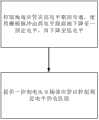
以下将说明采用上述实施例的GOA驱动电路10的驱动方法。请参照图6,图6为本发明一优选实施例的GOA驱动电路的驱动方法的流程图。本实施例的驱动方法用于产生驱动扫描线Gn的栅极脉冲Gp,所述栅极脉冲Gp具有一高电平Vgh及一低电平Vgl。所述GOA驱动电路10包括GOA控制单元120,耦接于所述GOA控制单元120与所述扫描线Gn之间的选择开关电路140,以及耦接于所述选择开关电路140的场效应管160。上述元件的具体说明以详述于上,在此不予以赘述。 A driving method of the
如图6所示,所述驱动方法包括步骤S10及S20。在步骤S10 中,控制所述场效应管160在所述高电平Vgh期间导通,使得所述栅极脉冲Gp由所述高电平Vgh倾斜地下降至一预定电平Vp,再下降至所述低电平Vgl,其中所述预定电平Vp介于所述高电平Vgh及所述低电平Vgl之间。 As shown in FIG. 6, the driving method includes steps S10 and S20. In step S10, the
在步骤S20中,提供一控制电压Vgh1至所述场效应管160以控制所述预定电平Vp的电压值,其中所述预定电平Vp的电压值等于所述控制电压Vgh1减掉一阈值电压Vth。由上述步骤则可达成削角的目的。 In step S20, a control voltage Vgh1 is provided to the
综上所述,本发明不更动电源芯片的设计,而是在GOA面板上设置了场效应管160,并根据第一时钟信号CLK1控制场效应管160的导通,以决定栅极脉冲Gp的削角宽度。另外,还可提供所述控制电压Vgh1,以决定所述预定电平Vp的电压值,即可控制削角的深度。因此,本发明无须采用复杂的电源芯片,而降低了生产成本。 In summary, the present invention does not change the design of the power supply chip, but sets the
虽然本发明已以优选实施例揭露如上,但上述优选实施例幷非用以限制本发明,本领域的普通技术人员,在不脱离本发明的精神和范围内,均可作各种更动与润饰,因此本发明的保护范围以权利要求界定的范围为准。 Although the present invention has been disclosed above with preferred embodiments, the above preferred embodiments are not intended to limit the present invention. Those skilled in the art can make various modifications and changes without departing from the spirit and scope of the present invention. Modification, therefore, the scope of protection of the present invention is subject to the scope defined by the claims. the
Claims (10)
Priority Applications (5)
| Application Number | Priority Date | Filing Date | Title |
|---|---|---|---|
| CN201310162954.8ACN103258514B (en) | 2013-05-06 | 2013-05-06 | GOA drive circuit and drive method |
| KR1020157033596AKR101824139B1 (en) | 2013-05-06 | 2013-06-25 | Goa drive circuit and drive method |
| PCT/CN2013/077853WO2014180031A1 (en) | 2013-05-06 | 2013-06-25 | Goa drive circuit and drive method |
| US13/985,579US20150154927A1 (en) | 2013-05-06 | 2013-06-25 | Gate driver-on-array driving circuit and driving method |
| GB1519050.7AGB2527715B (en) | 2013-05-06 | 2013-06-25 | Gate driver-on-array driving circuit and driving method |
Applications Claiming Priority (1)
| Application Number | Priority Date | Filing Date | Title |
|---|---|---|---|
| CN201310162954.8ACN103258514B (en) | 2013-05-06 | 2013-05-06 | GOA drive circuit and drive method |
Publications (2)
| Publication Number | Publication Date |
|---|---|
| CN103258514Atrue CN103258514A (en) | 2013-08-21 |
| CN103258514B CN103258514B (en) | 2015-05-20 |
Family
ID=48962390
Family Applications (1)
| Application Number | Title | Priority Date | Filing Date |
|---|---|---|---|
| CN201310162954.8AExpired - Fee RelatedCN103258514B (en) | 2013-05-06 | 2013-05-06 | GOA drive circuit and drive method |
Country Status (5)
| Country | Link |
|---|---|
| US (1) | US20150154927A1 (en) |
| KR (1) | KR101824139B1 (en) |
| CN (1) | CN103258514B (en) |
| GB (1) | GB2527715B (en) |
| WO (1) | WO2014180031A1 (en) |
Cited By (11)
| Publication number | Priority date | Publication date | Assignee | Title |
|---|---|---|---|---|
| CN105261320A (en)* | 2015-07-22 | 2016-01-20 | 京东方科技集团股份有限公司 | GOA unit drive circuit and driving method thereof, display panel and display apparatus |
| CN105529010A (en)* | 2016-02-18 | 2016-04-27 | 深圳市华星光电技术有限公司 | GOA circuit and liquid crystal display device |
| CN106128394A (en)* | 2016-08-31 | 2016-11-16 | 深圳市华星光电技术有限公司 | Display circuit and there is the LCDs of this display circuit |
| CN107342038A (en)* | 2017-09-13 | 2017-11-10 | 京东方科技集团股份有限公司 | A kind of shift register, its driving method, gate driving circuit and display device |
| CN107909958A (en)* | 2017-12-29 | 2018-04-13 | 武汉华星光电半导体显示技术有限公司 | GOA circuit units, GOA circuits and display panel |
| CN109523965A (en)* | 2018-12-19 | 2019-03-26 | 惠科股份有限公司 | Drive circuit, drive circuit of display panel and display device |
| US10304403B2 (en) | 2015-11-09 | 2019-05-28 | Boe Technology Group Co., Ltd. | Display apparatus and drive circuit thereof |
| CN111145702A (en)* | 2020-01-13 | 2020-05-12 | Tcl华星光电技术有限公司 | Clock signal modulation circuit and display panel |
| US10803779B2 (en) | 2017-12-29 | 2020-10-13 | Wuhan China Star Optoelectronics Semiconductor Display Technology Co., Ltd. | Gate driver on array (GOA) circuit unit, GOA circuit, and display panel |
| CN115641803A (en)* | 2022-11-02 | 2023-01-24 | 惠州华星光电显示有限公司 | Grid driving circuit and display panel |
| EP3185236B1 (en)* | 2014-08-18 | 2023-07-26 | BOE Technology Group Co., Ltd. | Goa circuit and drive method thereof, and display device |
Families Citing this family (5)
| Publication number | Priority date | Publication date | Assignee | Title |
|---|---|---|---|---|
| CN103390392B (en)* | 2013-07-18 | 2016-02-24 | 合肥京东方光电科技有限公司 | GOA circuit, array base palte, display device and driving method |
| CN104318888B (en)* | 2014-11-06 | 2017-09-15 | 京东方科技集团股份有限公司 | Array base palte drive element of the grid, method, circuit and display device |
| CN105096866A (en)* | 2015-08-07 | 2015-11-25 | 深圳市华星光电技术有限公司 | Liquid crystal display and control method thereof |
| CN106128408A (en)* | 2016-09-18 | 2016-11-16 | 深圳市华星光电技术有限公司 | The drive circuit of a kind of display panels and display panels |
| EP4318191A4 (en)* | 2021-03-26 | 2025-04-09 | Hideep Inc. | TOUCH INPUT DEVICE |
Citations (5)
| Publication number | Priority date | Publication date | Assignee | Title |
|---|---|---|---|---|
| JPH11352938A (en)* | 1998-06-09 | 1999-12-24 | Sharp Corp | Liquid crystal display device, driving method thereof, and scanning line driving circuit |
| JP2003216116A (en)* | 2002-01-23 | 2003-07-30 | Sharp Corp | Display device, its control method and portable information equipment incorporating the device |
| US20060152464A1 (en)* | 2005-01-12 | 2006-07-13 | Seiko Epson Corporation | Drive circuit of electro-optical device, driving method of electro-optical device, and electro-optical device having the same |
| CN101587700A (en)* | 2009-06-26 | 2009-11-25 | 友达光电股份有限公司 | Liquid crystal display and method of driving the same |
| CN201716968U (en)* | 2010-06-08 | 2011-01-19 | 青岛海信电器股份有限公司 | Angle cutting circuit and liquid crystal drive circuit with same |
Family Cites Families (16)
| Publication number | Priority date | Publication date | Assignee | Title |
|---|---|---|---|---|
| JP3037886B2 (en)* | 1995-12-18 | 2000-05-08 | インターナショナル・ビジネス・マシーンズ・コーポレイション | Driving method of liquid crystal display device |
| TWI330820B (en)* | 2006-01-26 | 2010-09-21 | Au Optronics Corp | Flat panel display and display panel thereof |
| TWI336461B (en)* | 2007-03-15 | 2011-01-21 | Au Optronics Corp | Liquid crystal display and pulse adjustment circuit thereof |
| CN101739974B (en)* | 2008-11-14 | 2012-07-04 | 群康科技(深圳)有限公司 | Pulse regulating circuit and driving circuit using same |
| CN100594413C (en)* | 2008-11-24 | 2010-03-17 | 上海广电光电子有限公司 | Liquid crystal display panel and driving method thereof |
| TWI410941B (en)* | 2009-03-24 | 2013-10-01 | Au Optronics Corp | Liquid crystal display capable of reducing image flicker and method for driving the same |
| TWI419106B (en)* | 2009-05-20 | 2013-12-11 | Au Optronics Corp | Level shift circuit, liquid crystal display device and charge sharing method |
| US8106873B2 (en)* | 2009-07-20 | 2012-01-31 | Au Optronics Corporation | Gate pulse modulation circuit and liquid crystal display thereof |
| CN101833931B (en)* | 2010-06-11 | 2012-02-22 | 友达光电股份有限公司 | Liquid crystal display device |
| TWI427610B (en)* | 2010-08-06 | 2014-02-21 | Au Optronics Corp | Liquid crystal display device with low power consumption and method for driving the same |
| TWI415051B (en)* | 2010-09-15 | 2013-11-11 | Au Optronics Corp | Lcd driving circuit and related driving method |
| CN102654982B (en)* | 2011-05-16 | 2013-12-04 | 京东方科技集团股份有限公司 | Shift register unit circuit, shift register, array substrate and liquid crystal display |
| TWI436332B (en)* | 2011-11-30 | 2014-05-01 | Au Optronics Corp | Display panel and gate driver therein |
| CN102779494B (en)* | 2012-03-29 | 2015-08-05 | 北京京东方光电科技有限公司 | A kind of gate driver circuit, method and liquid crystal display |
| CN102881272B (en)* | 2012-09-29 | 2015-05-27 | 深圳市华星光电技术有限公司 | Driving circuit, liquid crystal display device and driving method |
| TWI520493B (en)* | 2013-02-07 | 2016-02-01 | 友達光電股份有限公司 | Shift register circuit and shading waveform generating method |
- 2013
- 2013-05-06CNCN201310162954.8Apatent/CN103258514B/ennot_activeExpired - Fee Related
- 2013-06-25KRKR1020157033596Apatent/KR101824139B1/enactiveActive
- 2013-06-25WOPCT/CN2013/077853patent/WO2014180031A1/enactiveApplication Filing
- 2013-06-25GBGB1519050.7Apatent/GB2527715B/enactiveActive
- 2013-06-25USUS13/985,579patent/US20150154927A1/ennot_activeAbandoned
Patent Citations (5)
| Publication number | Priority date | Publication date | Assignee | Title |
|---|---|---|---|---|
| JPH11352938A (en)* | 1998-06-09 | 1999-12-24 | Sharp Corp | Liquid crystal display device, driving method thereof, and scanning line driving circuit |
| JP2003216116A (en)* | 2002-01-23 | 2003-07-30 | Sharp Corp | Display device, its control method and portable information equipment incorporating the device |
| US20060152464A1 (en)* | 2005-01-12 | 2006-07-13 | Seiko Epson Corporation | Drive circuit of electro-optical device, driving method of electro-optical device, and electro-optical device having the same |
| CN101587700A (en)* | 2009-06-26 | 2009-11-25 | 友达光电股份有限公司 | Liquid crystal display and method of driving the same |
| CN201716968U (en)* | 2010-06-08 | 2011-01-19 | 青岛海信电器股份有限公司 | Angle cutting circuit and liquid crystal drive circuit with same |
Cited By (22)
| Publication number | Priority date | Publication date | Assignee | Title |
|---|---|---|---|---|
| EP3185236B1 (en)* | 2014-08-18 | 2023-07-26 | BOE Technology Group Co., Ltd. | Goa circuit and drive method thereof, and display device |
| US10276087B2 (en) | 2015-07-22 | 2019-04-30 | Boe Technology Group Co., Ltd. | GOA unit driving circuit and driving method thereof, display panel and display device |
| WO2017012255A1 (en)* | 2015-07-22 | 2017-01-26 | 京东方科技集团股份有限公司 | Goa unit drive circuit and drive method therefor, display panel and display apparatus |
| CN105261320A (en)* | 2015-07-22 | 2016-01-20 | 京东方科技集团股份有限公司 | GOA unit drive circuit and driving method thereof, display panel and display apparatus |
| CN105261320B (en)* | 2015-07-22 | 2018-11-30 | 京东方科技集团股份有限公司 | GOA unit driving circuit and its driving method, display panel and display device |
| US10304403B2 (en) | 2015-11-09 | 2019-05-28 | Boe Technology Group Co., Ltd. | Display apparatus and drive circuit thereof |
| CN105529010A (en)* | 2016-02-18 | 2016-04-27 | 深圳市华星光电技术有限公司 | GOA circuit and liquid crystal display device |
| US10037740B2 (en) | 2016-02-18 | 2018-07-31 | Shenzhen China Star Optoelectronics Technology Co., Ltd. | GOA circuit and liquid crystal display device |
| CN106128394A (en)* | 2016-08-31 | 2016-11-16 | 深圳市华星光电技术有限公司 | Display circuit and there is the LCDs of this display circuit |
| WO2018040164A1 (en)* | 2016-08-31 | 2018-03-08 | 深圳市华星光电技术有限公司 | Display circuit and liquid crystal display screen having same |
| CN106128394B (en)* | 2016-08-31 | 2018-06-19 | 深圳市华星光电技术有限公司 | Display circuit and the liquid crystal display with the display circuit |
| US10276115B2 (en) | 2016-08-31 | 2019-04-30 | Shenzhen China Star Optoelectronics Technology Co., Ltd | Display circuit and LCD having the display circuit |
| US10685615B2 (en) | 2017-09-13 | 2020-06-16 | Boe Technology Group Co., Ltd. | Shift register and driving method thereof, gate driving circuit, and display device |
| CN107342038B (en)* | 2017-09-13 | 2021-04-02 | 京东方科技集团股份有限公司 | A shift register, its driving method, gate driving circuit and display device |
| CN107342038A (en)* | 2017-09-13 | 2017-11-10 | 京东方科技集团股份有限公司 | A kind of shift register, its driving method, gate driving circuit and display device |
| CN107909958A (en)* | 2017-12-29 | 2018-04-13 | 武汉华星光电半导体显示技术有限公司 | GOA circuit units, GOA circuits and display panel |
| US10803779B2 (en) | 2017-12-29 | 2020-10-13 | Wuhan China Star Optoelectronics Semiconductor Display Technology Co., Ltd. | Gate driver on array (GOA) circuit unit, GOA circuit, and display panel |
| CN109523965A (en)* | 2018-12-19 | 2019-03-26 | 惠科股份有限公司 | Drive circuit, drive circuit of display panel and display device |
| CN109523965B (en)* | 2018-12-19 | 2021-07-23 | 惠科股份有限公司 | Drive circuit, drive circuit of display panel and display device |
| CN111145702A (en)* | 2020-01-13 | 2020-05-12 | Tcl华星光电技术有限公司 | Clock signal modulation circuit and display panel |
| CN115641803A (en)* | 2022-11-02 | 2023-01-24 | 惠州华星光电显示有限公司 | Grid driving circuit and display panel |
| US12367804B2 (en) | 2022-11-02 | 2025-07-22 | Huizhou China Star Optoelectronics Display Co., Ltd. | Gate driving circuit and display panel |
Also Published As
| Publication number | Publication date |
|---|---|
| KR20160003102A (en) | 2016-01-08 |
| GB2527715A (en) | 2015-12-30 |
| WO2014180031A1 (en) | 2014-11-13 |
| GB201519050D0 (en) | 2015-12-09 |
| KR101824139B1 (en) | 2018-02-01 |
| US20150154927A1 (en) | 2015-06-04 |
| CN103258514B (en) | 2015-05-20 |
| GB2527715B (en) | 2020-08-26 |
Similar Documents
| Publication | Publication Date | Title |
|---|---|---|
| CN103258514B (en) | GOA drive circuit and drive method | |
| CN108766380B (en) | GOA circuit | |
| CN109427310B (en) | Shift register unit, driving device, display device and driving method | |
| CN101093647B (en) | Gate driving circuit and display apparatus having the same | |
| CN101520998B (en) | Liquid crystal display capable of improving image flicker and related driving method | |
| US10388241B2 (en) | Pixel charging method and circuit, LCD panel, and LCD device | |
| CN100428327C (en) | Shift register and its driving method | |
| US9666140B2 (en) | Display device and method for driving same | |
| CN103325353B (en) | For the level shifter of liquid crystal display | |
| US8552956B2 (en) | Liquid crystal display | |
| TWI540554B (en) | Liquid crystal display device and driving method thereof | |
| US20120139883A1 (en) | Gate drive circuit and display apparatus having the same | |
| CN108257578A (en) | Shift register cell and its control method, gate drive apparatus, display device | |
| CN102110405A (en) | Display device and method for controlling gate pulse modulation thereof | |
| CN102651208A (en) | Grid electrode driving circuit and display | |
| TW201525963A (en) | Display device and method of initializing gate shift register of the same | |
| KR101808338B1 (en) | Display device and method of controlling gate pulse thereof | |
| TWI482136B (en) | Gate driver circuit structure and display thereof | |
| CN102013244A (en) | Liquid crystal display driving circuit and related driving method | |
| CN106251803B (en) | Gate driver for display panel, display panel and display | |
| JP2009258733A (en) | Method and device for driving liquid crystal display | |
| KR20140109019A (en) | Gate driver module, display apparatus having the same and method of driving display panel using the same | |
| CN107331363A (en) | A kind of array base palte, its driving method and display device | |
| CN109741716A (en) | Data signal delay circuit and delay method, and display device | |
| KR20120031651A (en) | Display device and method of controlling clock signal thereof |
Legal Events
| Date | Code | Title | Description |
|---|---|---|---|
| C06 | Publication | ||
| PB01 | Publication | ||
| C10 | Entry into substantive examination | ||
| SE01 | Entry into force of request for substantive examination | ||
| C14 | Grant of patent or utility model | ||
| GR01 | Patent grant | ||
| CF01 | Termination of patent right due to non-payment of annual fee | ||
| CF01 | Termination of patent right due to non-payment of annual fee | Granted publication date:20150520 |