CN103248130A - Method for low-loss data transmission in high-power inductive power supply - Google Patents
Method for low-loss data transmission in high-power inductive power supplyDownload PDFInfo
- Publication number
- CN103248130A CN103248130ACN2012100265107ACN201210026510ACN103248130ACN 103248130 ACN103248130 ACN 103248130ACN 2012100265107 ACN2012100265107 ACN 2012100265107ACN 201210026510 ACN201210026510 ACN 201210026510ACN 103248130 ACN103248130 ACN 103248130A
- Authority
- CN
- China
- Prior art keywords
- power supply
- signal
- power
- circuit
- data
- Prior art date
- Legal status (The legal status is an assumption and is not a legal conclusion. Google has not performed a legal analysis and makes no representation as to the accuracy of the status listed.)
- Granted
Links
- 238000000034methodMethods0.000titleclaimsabstractdescription23
- 230000001939inductive effectEffects0.000titleclaimsabstractdescription20
- 230000005540biological transmissionEffects0.000titleclaimsdescription45
- 238000004458analytical methodMethods0.000claimsabstractdescription18
- 238000001514detection methodMethods0.000claimsabstractdescription18
- 230000006870functionEffects0.000claimsdescription25
- 239000003990capacitorSubstances0.000claimsdescription16
- 230000000087stabilizing effectEffects0.000claimsdescription10
- 238000007405data analysisMethods0.000claimsdescription5
- 238000001914filtrationMethods0.000claimsdescription5
- 230000007704transitionEffects0.000claimsdescription3
- 239000003638chemical reducing agentSubstances0.000claimsdescription2
- 230000005611electricityEffects0.000claims3
- 230000006698inductionEffects0.000abstractdescription4
- 238000010586diagramMethods0.000description19
- 230000008054signal transmissionEffects0.000description9
- 230000000694effectsEffects0.000description6
- 230000004048modificationEffects0.000description3
- 238000012986modificationMethods0.000description3
- 230000001360synchronised effectEffects0.000description3
- 230000007812deficiencyEffects0.000description2
- 238000013461designMethods0.000description2
- 238000011017operating methodMethods0.000description2
- 238000012545processingMethods0.000description2
- 230000009471actionEffects0.000description1
- 230000003139buffering effectEffects0.000description1
- 230000008859changeEffects0.000description1
- 238000006243chemical reactionMethods0.000description1
- 230000003993interactionEffects0.000description1
- 230000007257malfunctionEffects0.000description1
- 238000004519manufacturing processMethods0.000description1
- 238000005259measurementMethods0.000description1
- 239000002184metalSubstances0.000description1
- 230000008569processEffects0.000description1
Images


Landscapes
- Near-Field Transmission Systems (AREA)
Abstract
Description
Translated fromChinese技术领域technical field
本发明是提供一种高功率感应式电源供应器中数据低损耗传输的方法,尤指在进行感应式供应电源时,降低传输数据讯号的损耗的电源供应器,可使供电模块输出大功率、并可正确解析来自受电模块传送的数据讯号,稳定控制系统运作的功能。The present invention provides a low-loss data transmission method in a high-power inductive power supply, especially a power supply that reduces the loss of transmitted data signals when inductively supplying power, enabling the power supply module to output high power, And it can correctly analyze the data signal sent from the power receiving module, and stabilize the function of controlling the operation of the system.
背景技术Background technique
生活环境进入数字时代,各种数字式产品更充斥在生活周遭,例如数字相机、行动电话、音乐播放器(MP3、MP4)等各种可携式电子装置,且各种可携式电子装置、产品均朝向轻、薄、短、小的设计理念,但如要达到可随时携带使用目的首先必须要解决的即是用电的问题,一般最普遍的方式就是在可携式电子装置内装设充电电池,在电力耗尽时,能重新充电,但现今每个人都具有多个可携式电子装置,每个可携式电子装置都各自有特定相容的充电器,且充电器于使用时,必须以连接介面(插头)插接到电源插座,再将另一端的连接器插接到可携式电子装置,使其可携式电子装置进行充电,待充电完成后,才将充电器上的电子装置移除,然因充电器需要在有电源插座的地方才可进行电性插接、充电,导致充电地点受到限制,如果处于室外即无法进行充电。The living environment has entered the digital age, and various digital products are flooding around our lives, such as digital cameras, mobile phones, music players (MP3, MP4) and other portable electronic devices, and various portable electronic devices, The products are all oriented toward light, thin, short, and small design concepts, but to achieve the purpose of being portable at any time, the first thing that must be solved is the problem of power consumption. Generally, the most common way is to install charging devices in portable electronic devices. Batteries can be recharged when they run out of power, but today everyone has multiple portable electronic devices, and each portable electronic device has its own specific compatible charger, and when the charger is in use, The connection interface (plug) must be plugged into the power socket, and then the connector on the other end should be plugged into the portable electronic device, so that the portable electronic device can be charged. The electronic device is removed, but because the charger needs to be electrically plugged and charged in a place with a power socket, the charging location is limited, and it cannot be charged if it is outdoors.
又一般电子装置除了充电之外,也必须进行相关功能的设定或数据的编辑、传送等,除了通过电子装置直接进行设定、输入之外,有些电子装置(如:音乐播放器〔MP3、MP4等〕、数字相机、电子表、携带型游戏机、无线游戏手把、控制器等)并无法直接进行设定,必须通过另外的电子产品(电脑、个人数字助理等)才能进行功能设定、数据的传输,而一般电子装置在进行充电的同时,并无法同步进行数据的传输,必须分开进行;且目前市面上所推出的感应式电源供应器(或称无线式充电器)系利用二个线圈,其中一个作为发射电力的供电端,另一个当作接收电力的受电端进行运作,由于无线电力的能量具有危险性,会对金属物体加热,原理如同电磁炉,也影响被充电物体容易因受热造成损坏或故障的现象。In addition to charging, general electronic devices must also set related functions or edit and transmit data. In addition to directly setting and inputting through electronic devices, some electronic devices (such as: music players [MP3, MP4, etc.), digital cameras, electronic watches, portable game consoles, wireless game handles, controllers, etc.) cannot be set directly, and must be set through another electronic product (computer, personal digital assistant, etc.) , data transmission, and general electronic devices cannot synchronize data transmission while charging, and must be carried out separately; and the inductive power supply (or wireless charger) currently on the market uses two One of the coils, one of which is used as the power supply end for transmitting power, and the other operates as a power receiving end for receiving power. Because the energy of wireless power is dangerous, it will heat metal objects. The principle is like an induction cooker, and it is also easy to affect the charged object. Damage or malfunction due to heat.
而为了改善目前电子装置在进行充电时,无法同时传送必要的数据、以进行电子装置的目标识别或功能设定相关作业处理的缺失,则本案申请人曾于2011年2月1日,以『高功率感应式电源供应器中数据传输的方法』提呈中国台湾发明专利的申请,申请案号第100103836号,并提早供开于2011年7月1日的发明公开公报,公开编号第201123676号,该发明专利前案是本案申请人通过电源供应器的供电模块、受电模块之间,通过供电线圈与受电线圈相互感应,以进行电源、数据讯号的传输,并可降低电源传输的损耗率、数据讯号清晰传输、并具有极大的容错能力,但是因受电模块的调幅载波调制电路在进行调制数据讯号后,会消耗较大的电流,则在实际进行无线充电时,即存在有下列的缺失,如:In order to improve the lack of simultaneous transmission of necessary data for target identification or function setting of electronic devices when the current electronic devices are charging, the applicant in this case filed on February 1, 2011 with " The method of data transmission in high-power inductive power supply” submitted an application for an invention patent in Taiwan, China, application number 100103836, and provided an early publication of the invention on July 1, 2011, publication number 201123676 , the previous patent for this invention is that the applicant of this case uses mutual induction between the power supply module and the power receiving module of the power supply, and through the power supply coil and the power receiving coil to transmit power and data signals, and can reduce the loss of power transmission High rate, clear transmission of data signals, and great fault tolerance, but because the amplitude modulation carrier modulation circuit of the power receiving module consumes a large amount of current after modulating the data signal, there is a problem in actual wireless charging. The following are missing, such as:
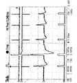
(1)受电模块的调幅载波调制电路,在调制数据讯号时,是从谐振电路的电容A 3前端拉取高电压再通过MOSFET元件导通接地(GND),因为电压高、所以通过的电流也会很大,造成线圈上的电力的较高消耗,所以在供电端数据解析电路13上解析出的数据波型大幅下陷(请同时参阅图12所示,其中3号波形中段向下骤降处),这也造成下受电端在数据波型下陷处的受电能力较弱。(1) The amplitude modulation carrier modulation circuit of the power receiving module, when modulating the data signal, pulls a high voltage from the front end of the capacitor A3 of the resonant circuit and then conducts the ground (GND) through the MOSFET element. Because the voltage is high, the current passing Also can be very big, cause the higher consumption of the electric power on the coil, so the data waveform analyzed on the
(2)在受电模块A利用调幅载波调制电路A 1进行数据讯号调制时(请参阅图13所示),会有高电压、高电流通过MOSFET元件A11,容易导致MOSFET元件A11烧毁,影响受电模块A的使用寿命缩短。(2) When the power receiving module A uses the AM carrier modulation circuit A1 to modulate the data signal (please refer to Figure 13), there will be high voltage and high current passing through the MOSFET element A11, which will easily cause the MOSFET element A11 to burn out and affect the affected The service life of the electrical module A is shortened.
(3)受电模块A在利用调幅载波调制电路A1进行数据讯号调制时,在受电模块A的主要电力回路中,通过整流器A2提供一条捷径,让交流电流不会通过谐振电路A3(谐振电容),则直接在受电线圈A4上进行短路的现象,可以供受电线圈A4产生的反馈讯号更清晰、易于辨识,然却会导致谐振电路A3后侧的电力回路在数据讯号调制期间完全失去供电能力,造成短暂断电的情况,影响受电输出端A5的电源输出在数据讯号调制期间不稳定。(3) When the power receiving module A uses the AM carrier modulation circuit A1 to modulate the data signal, in the main power circuit of the power receiving module A, a shortcut is provided through the rectifier A2 so that the AC current will not pass through the resonant circuit A3 (resonant capacitor ), the phenomenon of short-circuiting directly on the power receiving coil A4 can make the feedback signal generated by the power receiving coil A4 clearer and easier to identify, but it will cause the power circuit on the rear side of the resonant circuit A3 to completely lose during the modulation of the data signal Power supply capability, resulting in a short-term power failure, affects the instability of the power output of the power receiving output terminal A5 during the modulation of the data signal.
前述图12的数据讯号波形图中,左侧编号的说明:In the above-mentioned data signal waveform diagram of Figure 12, the description of the numbers on the left side:
编号1-是N型MOSFET元件242的控制讯号。Number 1 - is the control signal of the N-type MOSFET element 242 .
编号2-是N型MOSFET元件253的控制讯号。Number 2 - is the control signal of the N-type MOSFET element 253 .
编号3-是讯号解析电路13的输出讯号。Number 3 - is the output signal of the
编号4-是供电微处理器11判读结果的讯号。Number 4-is the signal for
因此,如何解决前案电源供应器在受电模块调制数据讯号时,影响电源传输中断、降低电源供应效能的问题与缺失,且受电模块的调幅载波调制电路会有高电压、高电流通过,造成MOSFET元件易烧毁的困扰,即为从事此行业的相关厂商所亟欲研究改善的方向所在。Therefore, how to solve the problems and deficiencies of the previous power supply that affect the interruption of power transmission and reduce the performance of power supply when the power receiving module modulates the data signal, and the amplitude modulation carrier modulation circuit of the power receiving module will pass high voltage and high current, The problem that MOSFET components are easy to burn out is the direction that relevant manufacturers in this industry want to study and improve.
发明内容Contents of the invention
故,发明人有鉴于上述的问题与缺失,乃搜集相关数据,经由多方评估及考量,并以从事于此行业累积的多年经验,经由不断试作及修改,始研发出此种可供电子装置同步进行供电、数据讯号传输,在受电输出端输出负载不稳定干扰受电模块反馈数据讯号,或在调幅载波调制电路反馈产生振铃现象干扰受电模块的反馈讯号数据,供电模块的供电线圈即接收具有干扰成份的数据讯号,仍然可以利用具有抗噪声功能的讯号解析软件,正确解析出受电模块传输数据讯号的原来正确数据码,而达到供电模块可以稳定控制系统运作、持续发送大功率能量至受电模块,以转换电能输出功能的高功率感应式电源供应器中数据低损耗传输的方法的发明专利诞生。Therefore, in view of the above-mentioned problems and deficiencies, the inventor collected relevant data, evaluated and considered in many ways, and based on years of experience accumulated in this industry, through continuous trial and modification, he developed this available electronic device. Synchronous power supply and data signal transmission, output load instability at the power receiving output terminal interferes with the feedback data signal of the power receiving module, or the feedback signal data of the power receiving module is disturbed by the ringing phenomenon in the feedback of the amplitude modulation carrier modulation circuit, the power supply coil of the power supply module That is to say, when receiving data signals with interference components, the signal analysis software with anti-noise function can still be used to correctly analyze the original correct data code of the data signal transmitted by the power receiving module, so that the power supply module can stably control the system operation and continuously send high power The invention patent of the method of data low-loss transmission in the high-power inductive power supply that converts the power output function of the energy to the power receiving module was born.
本发明的主要目的乃在于该电源供应器的供电模块,是由供电微处理器电性连接供电驱动单元、讯号解析电路、线圈电压检测电路、显示单元、供电单元及电源接地端,供电驱动单元再电性连接谐振电路、供电线圈,利用供电线圈感应受电模块的受电线圈进行电源、数据讯号的传输,且受电模块的受电微处理器电性连接电压侦测电路、断路保护电路、稳压电路、调幅载波调制电路、直流降压器及整流滤波电路、谐振电路,通过供电模块在接收受电模块所传送的反馈讯号,而由供电微处理器内建的具有抗噪声功能的讯号解析软件,在受电输出端输出负载不稳定干扰受电模块反馈数据讯号,或在调幅载波调制电路反馈产生振铃现象干扰受电模块的反馈讯号数据,则供电模块在接收具有干扰成份的数据讯号,即通过具有抗噪声功能的讯号解析软件,仍可正确解析出受电模块原正确数据码,而达到供电模块的供电单元可以稳定控制系统的运作,持续发送大功率能量到受电模块、进行转换电能输出功能的目的。The main purpose of the present invention is the power supply module of the power supply, which is electrically connected to the power supply drive unit, signal analysis circuit, coil voltage detection circuit, display unit, power supply unit and power ground terminal by the power supply microprocessor, and the power supply drive unit Then electrically connect the resonant circuit and the power supply coil, use the power supply coil to sense the power receiving coil of the power receiving module to transmit power and data signals, and the power receiving microprocessor of the power receiving module is electrically connected to the voltage detection circuit and the circuit breaker protection circuit , voltage stabilizing circuit, AM carrier modulation circuit, DC step-down converter and rectification filter circuit, resonant circuit, through the power supply module to receive the feedback signal sent by the power receiving module, and the built-in power supply microprocessor with anti-noise function Signal analysis software, the output load instability at the power receiving output terminal interferes with the feedback data signal of the power receiving module, or the ringing phenomenon is generated in the feedback of the amplitude modulation carrier modulation circuit and interferes with the feedback signal data of the power receiving module, then the power supply module receives the interference component Data signal, that is, through the signal analysis software with anti-noise function, the original correct data code of the power receiving module can still be correctly analyzed, and the power supply unit reaching the power supply module can stably control the operation of the system and continuously send high-power energy to the power receiving module , The purpose of converting electric energy output function.
本发明的次要目的乃在于该电源供应器的受电模块,重新安排调幅载波调制电路,使其在讯号调制期间MOSFET元件不会承受过高的导通电压导致烧毁,且在主电力回路上避免线圈端直接短路的现象,而达到讯号调制期间受电端供电能力不会中断,稳定后端电源输出的目的。The secondary purpose of the present invention is to re-arrange the amplitude modulation carrier modulation circuit in the power receiving module of the power supply, so that the MOSFET element will not be burned due to excessively high conduction voltage during signal modulation, and on the main power circuit Avoid the direct short circuit of the coil end, and achieve the purpose of not interrupting the power supply capacity of the receiving end during signal modulation and stabilizing the output of the back-end power supply.
为了达到上述目的,本发明公开一种高功率感应式电源供应器中数据低损耗传输的方法,其步骤是:In order to achieve the above purpose, the present invention discloses a method for low-loss data transmission in a high-power inductive power supply, the steps of which are:
(a)数据解析程序初始化;(a) data analysis program initialization;
(b)启动供电模块的系统主程序,清除记时器;(b) start the system main program of the power supply module, and clear the timer;
(c)等待供电模块的供电微处理器内建电压比较器,产生作业中断;(c) Waiting for the built-in voltage comparator of the power supply microprocessor of the power supply module to generate an operation interruption;
(d)判断与上次受电模块进行数据完成传送的时间的间隔,是否高于预设数据传送间隔时间的下限,若低于间隔时间的下限、即执行步骤(e),若高于间隔时间的下限、即执行步骤(f);(d) Judging whether the time interval between the last time the power receiving module completed the data transmission is higher than the lower limit of the preset data transmission interval time, if it is lower than the lower limit of the interval time, then execute step (e), if it is higher than the interval the lower limit of the time to perform step (f);
(e)离上次完成数据的时间太近,表示非为来自受电模块的数据讯号,为噪声、予以略过,并执行步骤(b);(e) If it is too close to the last data completion time, it means that it is not a data signal from the power receiving module, but it is noise, skip it, and perform step (b);
(f)检查触发讯号,是否离上次调制中讯号结束后的时间,高于设定的非调制讯号判读下限,若低于下限时间、即执行步骤(g),若高于下限时间、即执行步骤(h);(f) Check the trigger signal, whether the time from the end of the last modulation signal is higher than the set lower limit for non-modulation signal interpretation, if it is lower than the lower limit time, execute step (g), if it is higher than the lower limit time, that is perform step (h);
(g)判断为振铃现象的噪声,予以略过,并执行步骤(b);(g) The noise judged to be the ringing phenomenon is skipped, and step (b) is performed;
(h)执行数据码检查程序;(h) Execute the data code checking procedure;
(i)检查目前是否有开始讯号标记,若有开始讯号、即执行步骤(n),若无开始讯号、即执行步骤(j);(i) Check whether there is a start signal mark at present, if there is a start signal, then perform step (n), if there is no start signal, then perform step (j);
(j)检查目前讯号是否为开始长度,若是、即执行步骤(k),若否、即执行步骤(m);(j) Check whether the current signal is the initial length, if so, execute step (k), if not, execute step (m);
(k)检查为符合开始的长度,标记有开始讯号后执行步骤(c);(k) Check that it matches the length of the start, and execute step (c) after marking the start signal;
(m)数据讯号无法辨视,接收数据失败,清空计时器等待下一次数据解析,执行步骤(b);(m) The data signal cannot be identified, the data reception fails, clear the timer and wait for the next data analysis, and perform step (b);
(n)已有开始讯号标记准备接收下一个位元,停止计时器取回发生中断讯号的时间长度。(n) The start signal mark is ready to receive the next bit, stop the timer to retrieve the time length of the interrupt signal.
(p)通过转态触发,判断目前讯号状态,若为调制中讯号、即执行步骤(q),若非调制中讯号、即执行步骤(w);(p) Judge the current signal state through the transition trigger, if it is a signal under modulation, execute step (q), if it is not a signal under modulation, execute step (w);
(q)调制中讯号,检查逻辑是否符合[逻辑1]或[逻辑0]的调制中长度,若符合、即执行步骤(r),若不符合、即执行步骤(m);(q) Signal in modulation, check whether the logic conforms to the modulation length of [logic 1] or [logic 0], if yes, execute step (r), if not, execute step (m);
(r)数据讯号于长度范围内,将对应逻辑位元填入接收存储器中,执行步骤(s);(r) Fill the corresponding logical bits into the receiving memory within the length range of the data signal, and execute step (s);
(s)检查是否已收完指定的位元数,若未收完、即执行步骤(c),若已收完、即执行步骤(t);(s) Check whether the specified number of bits has been received, if not, execute step (c), if received, execute step (t);
(t)收到数据码,确认格式是否正确,若格式正确、即执行步骤(u),若格式错误、即执行步骤、即执行步骤(m);(t) Receive the data code, confirm whether the format is correct, if the format is correct, execute step (u), if the format is wrong, execute step, that is, execute step (m);
(u)接收数据完成,清空计时器使下一次收到讯号可以确认离本次数据传送完成的时间长度;(u) After receiving the data, clear the timer so that the next signal received can confirm the length of time from the completion of this data transmission;
(v)输出接收到数据码,提供系统使用、执行步骤(b);(v) output received data code, provide system use, and execute step (b);
(w)非调制讯号,检查逻辑是否符合[逻辑1]或[逻辑0]的非调制长度,若符合、即执行步骤(r),若不符合、即执行步骤(m)。(w) For non-modulated signals, check whether the logic conforms to the non-modulated length of [logic 1] or [logic 0]. If so, execute step (r), if not, execute step (m).
附图说明Description of drawings
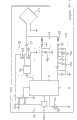
图1为本发明供电模块的简易电路图;Fig. 1 is a simple circuit diagram of the power supply module of the present invention;
图2为本发明受电模块的简易电路图;Fig. 2 is a simple circuit diagram of the power receiving module of the present invention;
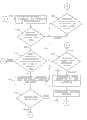
图3为本发明的步骤流程图(一);Fig. 3 is a flow chart (1) of steps of the present invention;
图4为本发明的步骤流程图(二);Fig. 4 is a flow chart of steps of the present invention (two);
图5为本发明的步骤流程图(三);Fig. 5 is a flow chart of steps of the present invention (3);
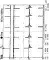
图6为本发明高功率输出的数据码波形图(一);Fig. 6 is a data code waveform diagram (1) of the high power output of the present invention;
图7为本发明高功率输出的数据码波形图(二);Fig. 7 is a data code waveform diagram (2) of the high power output of the present invention;
图8为本发明高功率输出的数据码波形图(三);Fig. 8 is a data code waveform diagram (3) of the high power output of the present invention;
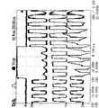
图9为本发明受电线圈的讯号波形图;Fig. 9 is a signal waveform diagram of the receiving coil of the present invention;
图10为本发明受电线圈的低功率输出讯号波形图;Fig. 10 is a low-power output signal waveform diagram of the power receiving coil of the present invention;
图11为本发明受电线圈的高功率输出讯号波形图;Fig. 11 is a high-power output signal waveform diagram of the receiving coil of the present invention;
图12为先申请案的数据讯号波形图;Fig. 12 is a data signal waveform diagram of the prior application;
图13为先申请案的受电模块简易电路图。FIG. 13 is a simplified circuit diagram of the power receiving module of the prior application.
附图标记说明:1-供电模块;11-供电微处理器;12-供电驱动单元;121-MOSFET驱动器;122-高端MOSFET元件;123-低端MOSFET元件;13-讯号解析电路;131-电阻;132-电容;133-整流二极管;14-线圈电压检测电路;141-电阻;142-电容;15-显示单元;16-供电单元;161-供电源;162-侦测用分压电阻;163-侦测用分压电阻;164-直流降压器;17-谐振电路;171-供电线圈;2-受电模块;21-受电微处理器;22-电压侦测电路;221-电阻;222-侦测端点;23-整流滤波电路;231-整流器;232-电容;24-调幅载波调制电路;241-电阻;242-N型MOSFET元件;25-断路保护电路;251-电阻;252-P型MOSFET元件;253-N型MOSFET元件;26-稳压电路;261-缓冲用电容;262-直流降压器;263-受电输出端;27-直流降压器;28-谐振电路;281-受电线圈;A-受电模块;A1-调幅载波调制电路;A11-MOSFET元件;A2-整流器;A3-谐振电路;A4-受电线圈;A5-受电输出端。Explanation of reference signs: 1-power supply module; 11-power supply microprocessor; 12-power supply drive unit; 121-MOSFET driver; 122-high-end MOSFET element; 123-low-end MOSFET element; 13-signal analysis circuit; 132-capacitor; 133-rectifier diode; 14-coil voltage detection circuit; 141-resistance; 142-capacitance; 15-display unit; 16-power supply unit; 161-power supply; -Divider resistor for detection; 164-DC step-down device; 17-resonant circuit; 171-power supply coil; 2-power receiving module; 21-power receiving microprocessor; 22-voltage detection circuit; 221-resistance; 222-detection endpoint; 23-rectifier filter circuit; 231-rectifier; 232-capacitor; 24-amplitude modulation carrier modulation circuit; 241-resistance; 242-N type MOSFET component; 25-open circuit protection circuit; P-type MOSFET component; 253-N-type MOSFET component; 26-stabilizing circuit; 261-capacitor for buffering; 262-DC step-down device; 281-power receiving coil; A-power receiving module; A1-amplitude modulation carrier modulation circuit; A11-MOSFET component; A2-rectifier; A3-resonant circuit; A4-power receiving coil; A5-power receiving output.
具体实施方式Detailed ways
为达成上述目的及功效,本发明所采用的技术手段及其构造,兹绘图就本发明的较佳实施例详加说明其特征、功能与实施方法如下,俾利完全了解。In order to achieve the above-mentioned purpose and effect, the technical means and the structure adopted by the present invention are hereby illustrated in detail with respect to the preferred embodiments of the present invention. Its features, functions and implementation methods are as follows, so that it can be fully understood.
请参阅图1至图5所示,为本发明供电模块的简易电路图、受电模块的简易电路图、步骤流程图(一)、步骤流程图(二)、步骤流程图(三),由图中所示可以清楚看出,本发明的无线感应装置包括供电模块1、受电模块2,其中:Please refer to Fig. 1 to Fig. 5, which are the simple circuit diagram of the power supply module of the present invention, the simple circuit diagram of the power receiving module, the step flow chart (1), the step flow chart (two), and the step flow chart (three), from the figure It can be clearly seen that the wireless induction device of the present invention includes a
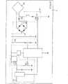
该供电模块1具有供电微处理器11,于供电微处理器11系内建有操作程序、控制程序、具有抗噪声功能的讯号解析软件等相关的软件程序,且供电微处理器11是分别电性连接供电驱动单元12、讯号解析电路13、线圈电压检测电路14、显示单元15、供电单元16,而供电驱动单元12系设有MOSFET驱动器121,且MOSFET驱动器121是分别连接于供电微处理器11、高端MOSFET元件122、低端MOSFET元件123,以通过高端MOSFET元件122、低端MOSFET元件123分别连接至谐振电路17,再通过高端MOSFET元件122电性连接电源单元16;至于讯号解析电路13是利用多个呈串、并联的电阻131、电容132再串联整流二极管133,以通过整流二极管133电性连接至谐振电路17;而供电单元16是分别连接有供电源161、呈串联的二侦测用分压电阻162、163、直流降压器164,且供电单元16电性连接于供电驱动单元12;并于谐振电路17连接有可传送电能、传输数据讯号的供电线圈171。This
该受电模块2是设有受电微处理器21,受电微处理器21设有操作程序、控制程序等相关软件程序,于受电微处理器21是分别连接于电压侦测电路22、整流滤波电路23、调幅载波调制电路24、断路保护电路25、稳压电路26、直流降压器27;且电压侦测电路22是具有串联式的多个电阻221电性连接于受电微处理器21,并利用串联式电阻221再分别串联侦测端点222、整流滤波电路23、断路保护电路25、直流降压器27;且整流滤波电路23为具有整流器231及电容232,分别并联电压侦测电路22、断路保护电路25及直流降压器27,再通过整流器231并联谐振电路28及受电线圈281;且受电线圈281则串连调幅载波调制电路24,而调幅载波调制电路24是具有串联的电阻241(亦可为电容)、N型MOFSET元件242;而断路保护电路25是串联电阻251、P型MOSFET元件252及N型MOSFET元件253,则利用N型MOSFET元件253,电性连接于受电微处理器21,另利用P型MOSFET元件252,电性连接于稳压电路26的缓冲用电容261、直流降压器262,则利用直流降压器262电性连接受电输出端263;而电压侦测电路22、断路保护电路25、稳压电路26及直流降压器27,分别电性连接于受电微处理器21,并利用电压侦测电路22、断路保护电路25及直流降压器27,分别电性连接于整流滤波电路23,再以整流滤波电路23的整流器231电性连接于谐振电路28,即由谐振电路28电性连接受电线圈281。The
而受电模块2的受电微处理器21,电性连接调幅载波调制电路24、断路保护电25,进行操作控制数据讯号,并利用受电微处理器21电性连接稳压路26,控制数据讯号通过时序安排,进行稳定的数据讯号传输,再经由供电模块1的供电微处理器11内建、具有抗噪声功能的讯号解析软件,使感应式电源供应器于电源传送中,由受电模块2反馈传送的数据讯号,以将损耗降至最低的受电端调幅载波调制电路24所产生的振铃现象噪声排除,使供电端可以进行正确的讯号解析,并在感应式电源供应器的受电模块2因放置不同预设电子产品(如:行动电话、个人数字助理〔PDA〕、笔记型电脑、数字相机、音乐播放器〔MP3、MP4等〕或掌上型游戏机等),造成受电模块2的负载电流快速变化时,也不会影响供电微处理器11的数据讯号解析,且受电模块2的电源转换电路与数据传输所使用的电路,是独立并分离,即可提升电源供应器的系统最大传送功率,并稳定系统运作的功能。The power receiving microprocessor 21 of the
则利用上述的供电模块1、受电模块2对预设电子装置进行供电与数据讯号传输的方法,其步骤系:Then use the above-mentioned
(100)进行数据解析程序初始化,是定义数据长度、开始讯号的长度、逻辑讯号条制与非调制长度、非调制讯号长度判读下限、数据传输间隔判读下限等。(100) Initialize the data analysis program, which is to define the data length, the length of the start signal, the length of the logic signal system and non-modulation, the lower limit of the non-modulated signal length, the lower limit of the data transmission interval, etc.
(101)启动供电模块1系统的主程序,清除计时器内容清除开始讯号标记后重新开始计时。(101) Start the main program of the
(102)供电微处理器11内建的电压比较器,等待数据讯号电压变化发生比较器产生中断后开始进行下一步骤。(102) The built-in voltage comparator of the
(103)发生比较器产生中断后判断与上一次受电模块2的数据讯号完成传送的时间的间隔,是否高于预设数据传送间隔时间的判读下限,若低于间隔时间的判读下限、即执行步骤(104),若高于间隔时间的判读下限、即执行步骤(105)。(103) After the comparator generates an interrupt, it is judged whether the time interval between the last data signal transmission of the
(104)离上一次完成数据传送的时间太近,表示非为来自受电模块2的数据讯号,为噪声、予以略过,并执行步骤(101)。(104) It is too close to the last data transmission time, indicating that it is not a data signal from the
(105)检查触发讯号,是否离上一次调制讯号结束后的时间,与设定的非调制讯号判读下限,若低于下限时间、即执行步骤(106),若高于下限时间、即执行步骤(107)。(105) Check the trigger signal, whether it is the time after the end of the last modulated signal, and the set lower limit for the interpretation of the non-modulated signal. If it is lower than the lower limit time, step (106) is executed. If it is higher than the lower limit time, step (106) is executed. (107).
(106)发生比较器电压中断离上一次调制讯号结束后的时间太近,判断为振铃现象的噪声,予以略过,并执行步骤(101)。(106) The time when the comparator voltage interruption is too close to the end of the last modulation signal, it is judged as the noise of the ringing phenomenon, it is skipped, and the step (101) is executed.
(107)发生比较器电压中断离上一次数据完成传送与上一次调制讯号结束时间长于判读设定下限值,确认为正确数据码讯号,执行数据码检查程序。(107) When the voltage of the comparator is disconnected, the time between the completion of the last data transmission and the end of the last modulation signal is longer than the lower limit value of the judgment setting, confirm that it is a correct data code signal, and execute the data code inspection program.
(108)检查目前是否有开始讯号,若有开始讯号、即执行步骤(112),若无开始讯号、即执行步骤(109)。(108) Check whether there is a start signal at present, if there is a start signal, then step (112) is executed, if there is no start signal, then step (109) is executed.
(109)检查目前讯号是否为开始长度,若是、即执行步骤(110),若否、即执行步骤(111)。(109) Check whether the current signal is the initial length, if so, execute step (110), if not, execute step (111).
(110)检查是为符合开始的长度,标记有开始讯号供下一次发生比较器中断识别为有开始接收位元,使下一次收到讯号开始接收位元数据,执行步骤(102)等待下一次中断。(110) The check is to match the length of the start, and the start signal is marked for the next comparator interrupt to be recognized as having a start receiving bit, so that the next time the signal is received, the bit data is started to be received, and step (102) is executed to wait for the next time interruption.
(111)供电微处理器11判断接收的数据讯号无法辨视,接收数据失败,执行步骤(100)清空计时器等待下一次发生比较器中断再开始数据解析。(111) The
(112)已有开始讯号标记准备接收下一个位元数据讯号,停止计时器取回发生中断讯号的时间长度。(112) The start signal mark is ready to receive the next bit data signal, and the timer is stopped to retrieve the time length of the interrupt signal.
(113)通过讯号解析电路13侦测到的比较器电压转态触发,判断目前讯号状态,若为调制中讯号、即执行步骤(114),若非调制中讯号、即执行步骤(120)。(113) Triggering by the comparator voltage transition detected by the
(114)判断目前接收到的时间长度为调制中的数据讯号,检查的时间长度的逻辑是否符合[逻辑1]或[逻辑0]的调制中长度设定范围,若符合、即执行步骤(115),若不符合、即执行步骤(111)。(114) Judging that the currently received time length is a data signal in modulation, whether the logic of the checked time length meets the length setting range in modulation of [logic 1] or [logic 0], if so, execute step (115) ), if not, execute step (111).
(115)所侦测的的时间长度,于时间长度设定范围内,将收到对应逻辑位元的的填入到接收存储器中,执行步骤(116)。(115) The detected time length is within the time length setting range, and the received corresponding logic bit is filled into the receiving memory, and step (116) is executed.
(116)检查是否已收完指定的位元数,若未收完、即执行步骤(102)等待下一次比较器中断,若已收完、即执行步骤(117)。(116) Check whether the specified number of bits has been received, if not received, then perform step (102) and wait for the next comparator interrupt, if received, then perform step (117).
(117)将指定的位元数存成数据码,将接收到的数据码确认格式是否正确,若格式正确、即执行步骤(118),若格式错误、即执行步骤(111)。(117) deposit the specified number of bits into data codes, and confirm whether the format of the received data codes is correct, if the format is correct, then step (118) is executed, if the format is wrong, then step (111) is executed.
(118)确认接收数据完成,清空数据传送完成计时器,使下一次发生比较中断时可以确认离本次数据传送完成的时间长度。(118) Confirm that the receiving data is completed, and clear the data transmission completion timer, so that the time length from the completion of this data transmission can be confirmed when the comparison interrupt occurs next time.
(119)输出接收到数据码,提供予供电模块1的系统使用、执行步骤(101)准备接收下一个数据讯号。(119) Outputting the received data code, providing it to the system of the
(120)判断目前接收到的时间长度为非调制中讯号,检查是否符合[逻辑1]或[逻辑0]的非调制中长度设定范围,若符合、即执行步骤(115),若不符合、即执行步骤(111)。(120) Judging that the currently received time length is a non-modulating signal, check whether it meets the non-modulating length setting range of [logic 1] or [logic 0], if it meets, then execute step (115), if not , that is, step (111) is executed.
上述本发明的电源供应器,于供应电源同时进行数据讯号传输,通过受电模块2的调幅载波调制电路24,在高功率系统中产生对接收电源损耗较低的零件配置安排,由受电模块2的受电线圈281传送反馈数据讯号,至供电模块1的供电线圈171,并由讯号解析电路13进行解码后,传送至供电微处理器11,利用供电微处理器11内建具有抗噪声功能的讯号解析软件排程,以正确解析由受电模块2反馈讯号数据,达到供应电源与传输数据讯号作业同步进行,并降低数据讯号传输的损耗现象。在受电模块2的受电输出端263输出负载不稳定下,干扰受电输模块2的受电线圈281传输的反馈数据讯号,则供电模块1的供电线圈171在接收具有干扰成份的数据讯号时,仍可通过供电模块1的供电微处理器11,以内建具有抗噪声功能的讯号解析软件,正确解析出受电模块2所反馈的数据讯号的原正确数据码,以达到供电模块1的供电单元16可以稳定控制系统运作,并持续发送大功率能量至受电模块2,而由受电模块转换电能后,通过受电输出端263对外输出、稳定供应电源。The above-mentioned power supply of the present invention performs data signal transmission while supplying power, and through the amplitude modulation
而受电模块21的调幅载波调制电路24,传送至接地端(GND)的讯号,是属于电压较低的直流方波,则调幅载波调制电路24的N型MOSFET元件242,不易烧毁,且调幅载波调制电路24未连接谐振电路25(电容)与受电线圈281之间,并在调幅载波调制电路24进行讯号调制中,不会影响受电模块2的电源接收能力,也不会造成电源与数据讯号在受电线圈281的回路中,产生短路的现象;且在调幅载波调制电路24调制后的讯号,于传输至供电模块1时,会产生振铃现象的噪声,即必须利用供电微处理器11内建的具有抗噪声功能的讯号解析软件排程,排除具有振铃噪声成份的讯号,亦同时将受电模块2因负载变化所产生的噪声一并排除。And the amplitude modulation
请参阅图6至图8所示,为本发明高功率输出的数据码波形图(一)、数据码波形图(二)、数据码波形图(三),由图中所示可以清楚看出,本发明供电模块1供应电源至受电模块2,并由受电模块2通过受电线圈281反馈数据讯号至供电模块1的供电线圈171,而供电线圈171将接收的数据讯号,通过讯号解析电路13进行讯号解析处理后,电源损耗较低的幅载波调制电路24使电压下陷情况轻微,解析后的数据讯号再传送至供电微处理器11用软件分析,此时供电单元16仍持续供电,由供电线圈171传送至受电线圈281,电源损耗较低零件配置安排的受电模块2的幅载波调制电路24中N型MOSFET元件242、断路保护电路25的N型MOSFET元件253的开关讯号,形成的反馈讯号速度反应快,在高功率传输情形下,产生振铃现象会造成反馈数据讯号的干扰,使供电模块1的讯号解析电路13的讯号解析,受到振铃现象的影响,而通过供电微处理器11内建具有抗噪声功能的讯号解析软件,将振铃现象产生的干扰噪声予以排除,而使讯号解析电路13仅解析出第一道数据讯号,后续的振铃现象的噪声即被忽略,则供电微处理器11内建比较器发生电压比较中断时不会误判数据讯号将其当作数据码,由供电单元16持续通过供电线圈171供应电源至受电模块2,而使受电模块2受电功能不会被影响,并可达到稳定的控制系统运作的功能。Please refer to Figures 6 to 8, which are the data code waveform diagram (1), the data code waveform diagram (2), and the data code waveform diagram (3) of the high power output of the present invention, which can be clearly seen from the figures The
而在图6至图8中,左侧编号的说明:In Figure 6 to Figure 8, the description of the numbers on the left side:
编号1-是N型MOSFET元件242的控制讯号。Number 1 - is the control signal of the N-type MOSFET element 242 .
编号2-是N型MOSFET元件253的控制讯号。Number 2 - is the control signal of the N-type MOSFET element 253 .
编号3-是讯号解析电路13的输出讯号。Number 3 - is the output signal of the
编号4-是供电微处理器11判读结果的讯号。Number 4-is the signal for
且在图9至11中,左侧编号的说明:And in Figures 9 to 11, the description of the numbers on the left side:
编号1-是谐振电路28(电容)至整流器231的端点间的讯号。Number 1 - is the signal between the terminal of the resonant circuit 28 (capacitor) and the rectifier 231 .
编号2-是受电线圈281至谐振电路28的端点间的讯号。Number 2 - is the signal between the receiving coil 281 and the terminal of the resonant circuit 28 .
编号3-是受电线圈281至整流器231的端点间的讯号。Number 3 - is the signal between the terminals of the power receiving coil 281 and the rectifier 231 .
编号4-是N型MOSFET元件242的控制讯号。Number 4 - is the control signal of the N-type MOSFET element 242 .
请参阅图9至11所示,为本发明受电线圈的讯号波形图、受电线圈的低功率输出讯号波形图、受电线圈的高功率输出讯号波形图,由图中所示可以清楚看出,本发明的受电模块2的受电线圈281一端,是连接于调幅载波电路24的电阻241(亦可由电容取代)、N型MOSFET元件242而连接至接地(GND)及整流滤波电路23的整流器231一端,且受电线圈281的另一端即连接谐振电路28(电容)后,再连接至整流滤波电路23的整流器231另一端,则在调幅载波调制电路24进行调制讯号中,受电线圈281一端连接整流器231的回路,数据讯号已被损耗,而受电线圈281一端连接于谐振电路28(电容)的回路,依然正常供应电源,以将受电线圈281自供电线圈171所接收的电源,供应至后端的受电微处理器21、电压侦测电路22、断路保护电路25、稳压电路26及直流降压器27,保持正常电源供应,而受电模块2若在低功率输出状态中,于调幅载波调制电路24进行调制讯号后,受电线圈281上的讯号可以快速恢复正常运作,可降低数据传输的损耗现象;且受电模块2若在高功率输出情况时,于调幅载波调制电路24进行调制讯号中,受电线圈281产生较大的负载效应,即可通过供电微处理器11内建具有抗噪声功能的讯号解析软件排程,排除振铃现象的噪声,且调制讯号结束后,受电线圈281亦可快速恢复正常运作,并可降低数据传输造成电源的损耗现象。Please refer to Figures 9 to 11, which are the signal waveform diagram of the power receiving coil, the low power output signal waveform diagram of the power receiving coil, and the high power output signal waveform diagram of the power receiving coil of the present invention, which can be clearly seen from the figures One end of the power receiving coil 281 of the power receiving module 2 of the present invention is connected to the resistor 241 of the AM carrier circuit 24 (it can also be replaced by a capacitor), the N-type MOSFET element 242 and connected to the ground (GND) and the rectification filter circuit 23 One end of the rectifier 231, and the other end of the power receiving coil 281 is connected to the resonant circuit 28 (capacitor), and then connected to the other end of the rectifier 231 of the rectification filter circuit 23, then in the modulation signal of the amplitude modulation carrier modulation circuit 24, the power receiving One end of the coil 281 is connected to the circuit of the rectifier 231, the data signal has been lost, and one end of the power receiving coil 281 is connected to the circuit of the resonant circuit 28 (capacitor), and the power supply is still normal, so that the power receiving coil 281 is received from the power supply coil 171. The power supply is supplied to the power receiving microprocessor 21, the voltage detection circuit 22, the circuit
因此,以上所述仅为本发明的较佳实施例而已,非因此局限本发明的专利范围,本发明高功率感应式电源供应器数据低损耗传输的方法,其是通过供电模块1的供电微处理器11供应电源至受电模块2的受电线圈281,而受电模块2所传输的数据讯号,通过受电线圈281反馈至供电模块1的供电线圈171,因受电输出端263输出负载不稳定干扰受电模块2反馈数据讯号,则由供电模块1的供电微处理器11内建具有抗噪声功能的讯号解析软件,让供电模块1在传送电源时,数据讯号能稳定传输,可达到降低数据讯号传输的损耗、并不影响供电模块1、受电模块2间电源供应的目的,并利用受电模块2的受电线圈281未连接谐振电路28(电容)的一端,连接至调幅载波调制电路24,在电压较低的直流方波上进行调制动作,则调幅载波调制电路24的N型MOSFET元件242,较不易被高电压或高电流烧毁,使供电源稳定供应至受电模块2,并可提升感应式供电源供应器的最大传送功率的优点,则通过供电微处理器11内建软件程序,排除供电模块1、受电模块2间,因振铃现象的噪声与供应电源相互干扰,亦达到同步进行充电与稳定传输数据讯号的实用功效,故举凡可达成前述效果的流程、实施方法等,及相关的设备、装置,皆应受本发明所涵盖,此种简易修饰及等效结构变化,均应同理包含于本发明的专利范围内,合予陈明。Therefore, the above description is only a preferred embodiment of the present invention, and does not limit the patent scope of the present invention. The method for low-loss data transmission of a high-power inductive power supply in the present invention is to use the power supply micro of the power supply module 1 The processor 11 supplies power to the power receiving coil 281 of the power receiving module 2, and the data signal transmitted by the power receiving module 2 is fed back to the power supply coil 171 of the power supply module 1 through the power receiving coil 281, because the power receiving output terminal 263 outputs a load If the unstable interference power receiving module 2 feeds back the data signal, then the power supply microprocessor 11 of the power supply module 1 has a built-in signal analysis software with anti-noise function, so that when the power supply module 1 transmits power, the data signal can be transmitted stably, which can reach Reduce the loss of data signal transmission without affecting the purpose of power supply between the power supply module 1 and the power receiving module 2, and use the end of the power receiving coil 281 of the power receiving module 2 that is not connected to the resonant circuit 28 (capacitor) to connect to the AM carrier The modulation circuit 24 performs the modulation action on the DC square wave with a lower voltage, and the N-type MOSFET element 242 of the amplitude modulation carrier modulation circuit 24 is less likely to be burned by high voltage or high current, so that the power supply can be stably supplied to the power receiving module 2 , and can improve the maximum transmission power of the inductive power supply, the built-in software program of the power supply microprocessor 11 eliminates the interaction between the power supply module 1 and the power receiving module 2 due to the noise caused by the ringing phenomenon and the power supply Interference can also achieve the practical effect of synchronous charging and stable transmission of data signals. Therefore, all processes, implementation methods, etc., and related equipment and devices that can achieve the aforementioned effects should be covered by the present invention. This simple modification and etc. Effect structure changes, all should be included in the patent scope of the present invention in the same way, and should be stated together.
上述本发明的感应式电源供应器中数据低损耗传输的方法,于实际实施制造作业时,为可具有下列各项优点,如:The above-mentioned low-loss data transmission method in the inductive power supply of the present invention can have the following advantages when actually implementing manufacturing operations, such as:
(一)供电模块1的供电微处理器11,是内建有具有抗噪声功能的讯号解析软件,可针对受电模块2反馈至供电模块1的数据讯号,排除干扰的噪声,而不影响供电模块1的电源供应至受电模块2,并降低供电模块2反馈数据讯号传输的损耗。(1) The
(二)受电模块2的受电线圈281,是分别电性连接调幅载波调制电路24、整流滤波电路23的整流器231及谐振电路28(电容)、整流器231的另一端,以将供电模块1的供电线圈171传送的电源,通过调幅载波调制电路24时、以低电压的直流方波流通,不致造成N型MOSFET元件242的烧毁。(2) The power receiving coil 281 of the
(三)供电模块1的讯号解析电路13,将接收讯号进行解析后,将振铃现象产生的噪声通过供电微处理器11内建具有抗噪声功能的讯号解析软件,可以正确解析出受电模块原正确数据码,使感应式电源供应器的供电模块1稳定供电至受电模块2,具有稳定电源供应及降低数据讯号传输损耗的功效。(3) The
因此,本发明为主要针对高功率感应器的数据低损耗传输方法的设计,为通过供电模块的供电微处理器内建具有抗噪声功能的讯号解析软件,可在受电模块反馈数据讯号至供电模块时,即由供电微处理器内建抗噪声的讯号解析电路,排除噪声干扰,而达到供电模块供电至受电模块的电源传送中、降低数据讯号传输损耗为主要保护重点,且稳定电源传送的系统运作,而具有同步稳定传送电源及传输数据讯号的功能,但是,以上所述仅为本发明的较佳实施例而已,非因此即局限本发明的专利范围,故举凡运用本发明说明书及图式内容所为的简易修饰、替换及等效原理变化,均应同理包含于本发明的专利范围内,合予陈明。Therefore, the present invention is mainly aimed at the design of a low-loss data transmission method for high-power sensors. The power supply microprocessor of the power supply module has a built-in signal analysis software with anti-noise function, which can feed back data signals to the power supply in the power receiving module. In the case of the module, the power supply microprocessor has a built-in anti-noise signal analysis circuit to eliminate noise interference, so as to achieve the power transmission from the power supply module to the power receiving module, reduce the data signal transmission loss as the main protection focus, and stabilize the power transmission system operation, and has the function of synchronously and stably transmitting power and transmitting data signals, but the above description is only a preferred embodiment of the present invention, and does not limit the patent scope of the present invention. The simple modifications, replacements and equivalent principle changes of the content of the drawings should be included in the scope of the patent of the present invention in the same way, and are hereby stated.
Claims (7)
Translated fromChinesePriority Applications (1)
| Application Number | Priority Date | Filing Date | Title |
|---|---|---|---|
| CN201210026510.7ACN103248130B (en) | 2012-02-07 | 2012-02-07 | Method for low-loss data transmission in high-power inductive power supply |
Applications Claiming Priority (1)
| Application Number | Priority Date | Filing Date | Title |
|---|---|---|---|
| CN201210026510.7ACN103248130B (en) | 2012-02-07 | 2012-02-07 | Method for low-loss data transmission in high-power inductive power supply |
Publications (2)
| Publication Number | Publication Date |
|---|---|
| CN103248130Atrue CN103248130A (en) | 2013-08-14 |
| CN103248130B CN103248130B (en) | 2014-12-17 |
Family
ID=48927428
Family Applications (1)
| Application Number | Title | Priority Date | Filing Date |
|---|---|---|---|
| CN201210026510.7AActiveCN103248130B (en) | 2012-02-07 | 2012-02-07 | Method for low-loss data transmission in high-power inductive power supply |
Country Status (1)
| Country | Link |
|---|---|
| CN (1) | CN103248130B (en) |
Cited By (16)
| Publication number | Priority date | Publication date | Assignee | Title |
|---|---|---|---|---|
| CN105045330A (en)* | 2015-06-30 | 2015-11-11 | 富达通科技股份有限公司 | Power supply module in induction type power supply and signal analysis circuit thereof |
| US9413197B2 (en) | 2010-05-31 | 2016-08-09 | Fu Da Tong Technology Co., Ltd. | Inductive power supply system and intruding metal detection method thereof |
| US9600021B2 (en) | 2011-02-01 | 2017-03-21 | Fu Da Tong Technology Co., Ltd. | Operating clock synchronization adjusting method for induction type power supply system |
| US9628147B2 (en) | 2011-02-01 | 2017-04-18 | Fu Da Tong Technology Co., Ltd. | Method of automatically adjusting determination voltage and voltage adjusting device thereof |
| US9671444B2 (en) | 2011-02-01 | 2017-06-06 | Fu Da Tong Technology Co., Ltd. | Current signal sensing method for supplying-end module of induction type power supply system |
| US9831687B2 (en) | 2011-02-01 | 2017-11-28 | Fu Da Tong Technology Co., Ltd. | Supplying-end module for induction-type power supply system and signal analysis circuit therein |
| US9960639B2 (en) | 2015-01-14 | 2018-05-01 | Fu Da Tong Technology Co., Ltd. | Supplying-end module of induction type power supply system and voltage measurement method thereof |
| CN108306838A (en)* | 2017-01-11 | 2018-07-20 | 联发科技(新加坡)私人有限公司 | Demodulator and the method for modulating input signal for solving modulation |
| US10038338B2 (en) | 2011-02-01 | 2018-07-31 | Fu Da Tong Technology Co., Ltd. | Signal modulation method and signal rectification and modulation device |
| US10056944B2 (en) | 2011-02-01 | 2018-08-21 | Fu Da Tong Technology Co., Ltd. | Data determination method for supplying-end module of induction type power supply system and related supplying-end module |
| US10114396B2 (en) | 2015-10-28 | 2018-10-30 | Fu Da Tong Technology Co., Ltd. | Induction type power supply system and intruding metal detection method thereof |
| US10153665B2 (en) | 2015-01-14 | 2018-12-11 | Fu Da Tong Technology Co., Ltd. | Method for adjusting output power for induction type power supply system and related supplying-end module |
| US10289142B2 (en) | 2011-02-01 | 2019-05-14 | Fu Da Tong Technology Co., Ltd. | Induction type power supply system and intruding metal detection method thereof |
| US10312748B2 (en) | 2011-02-01 | 2019-06-04 | Fu Da Tong Techology Co., Ltd. | Signal analysis method and circuit |
| US10615645B2 (en) | 2011-02-01 | 2020-04-07 | Fu Da Tong Technology Co., Ltd | Power supply device of induction type power supply system and NFC device identification method of the same |
| US10630113B2 (en) | 2011-02-01 | 2020-04-21 | Fu Da Tong Technology Co., Ltd | Power supply device of induction type power supply system and RF magnetic card identification method of the same |
Citations (3)
| Publication number | Priority date | Publication date | Assignee | Title |
|---|---|---|---|---|
| TW201123676A (en)* | 2011-02-01 | 2011-07-01 | Fu Da Tong Technology Co Ltd | Data transmission method of high-power induction type power supply device. |
| TW201134053A (en)* | 2011-06-07 | 2011-10-01 | Fu Da Tong Technology Co Ltd | Biphase decoding method for high-power induction type power supply |
| US20110264945A1 (en)* | 2010-04-26 | 2011-10-27 | Fu Da Tong Technology Co., Ltd. | Power supplying and data transmitting method for induction type power supply system |
- 2012
- 2012-02-07CNCN201210026510.7Apatent/CN103248130B/enactiveActive
Patent Citations (3)
| Publication number | Priority date | Publication date | Assignee | Title |
|---|---|---|---|---|
| US20110264945A1 (en)* | 2010-04-26 | 2011-10-27 | Fu Da Tong Technology Co., Ltd. | Power supplying and data transmitting method for induction type power supply system |
| TW201123676A (en)* | 2011-02-01 | 2011-07-01 | Fu Da Tong Technology Co Ltd | Data transmission method of high-power induction type power supply device. |
| TW201134053A (en)* | 2011-06-07 | 2011-10-01 | Fu Da Tong Technology Co Ltd | Biphase decoding method for high-power induction type power supply |
Cited By (17)
| Publication number | Priority date | Publication date | Assignee | Title |
|---|---|---|---|---|
| US9413197B2 (en) | 2010-05-31 | 2016-08-09 | Fu Da Tong Technology Co., Ltd. | Inductive power supply system and intruding metal detection method thereof |
| US10038338B2 (en) | 2011-02-01 | 2018-07-31 | Fu Da Tong Technology Co., Ltd. | Signal modulation method and signal rectification and modulation device |
| US10289142B2 (en) | 2011-02-01 | 2019-05-14 | Fu Da Tong Technology Co., Ltd. | Induction type power supply system and intruding metal detection method thereof |
| US9628147B2 (en) | 2011-02-01 | 2017-04-18 | Fu Da Tong Technology Co., Ltd. | Method of automatically adjusting determination voltage and voltage adjusting device thereof |
| US9671444B2 (en) | 2011-02-01 | 2017-06-06 | Fu Da Tong Technology Co., Ltd. | Current signal sensing method for supplying-end module of induction type power supply system |
| US9831687B2 (en) | 2011-02-01 | 2017-11-28 | Fu Da Tong Technology Co., Ltd. | Supplying-end module for induction-type power supply system and signal analysis circuit therein |
| US10630113B2 (en) | 2011-02-01 | 2020-04-21 | Fu Da Tong Technology Co., Ltd | Power supply device of induction type power supply system and RF magnetic card identification method of the same |
| US9600021B2 (en) | 2011-02-01 | 2017-03-21 | Fu Da Tong Technology Co., Ltd. | Operating clock synchronization adjusting method for induction type power supply system |
| US10615645B2 (en) | 2011-02-01 | 2020-04-07 | Fu Da Tong Technology Co., Ltd | Power supply device of induction type power supply system and NFC device identification method of the same |
| US10056944B2 (en) | 2011-02-01 | 2018-08-21 | Fu Da Tong Technology Co., Ltd. | Data determination method for supplying-end module of induction type power supply system and related supplying-end module |
| US10312748B2 (en) | 2011-02-01 | 2019-06-04 | Fu Da Tong Techology Co., Ltd. | Signal analysis method and circuit |
| US10153665B2 (en) | 2015-01-14 | 2018-12-11 | Fu Da Tong Technology Co., Ltd. | Method for adjusting output power for induction type power supply system and related supplying-end module |
| US9960639B2 (en) | 2015-01-14 | 2018-05-01 | Fu Da Tong Technology Co., Ltd. | Supplying-end module of induction type power supply system and voltage measurement method thereof |
| CN105045330A (en)* | 2015-06-30 | 2015-11-11 | 富达通科技股份有限公司 | Power supply module in induction type power supply and signal analysis circuit thereof |
| US10114396B2 (en) | 2015-10-28 | 2018-10-30 | Fu Da Tong Technology Co., Ltd. | Induction type power supply system and intruding metal detection method thereof |
| CN108306838A (en)* | 2017-01-11 | 2018-07-20 | 联发科技(新加坡)私人有限公司 | Demodulator and the method for modulating input signal for solving modulation |
| CN108306838B (en)* | 2017-01-11 | 2020-12-11 | 联发科技(新加坡)私人有限公司 | Demodulator and method for demodulating amplitude modulated input signal |
Also Published As
| Publication number | Publication date |
|---|---|
| CN103248130B (en) | 2014-12-17 |
Similar Documents
| Publication | Publication Date | Title |
|---|---|---|
| CN103248130B (en) | Method for low-loss data transmission in high-power inductive power supply | |
| TWI429165B (en) | Method of data transmission in high power | |
| TWI408861B (en) | Method of data transmission to induction power supply | |
| CN102315692B (en) | Power Transmission Method for High Power Wireless Inductive Power Supply | |
| CN102270872B (en) | Light sensor charger identification method | |
| CN202034798U (en) | Portable wireless charging device | |
| JP4725611B2 (en) | Power transmission control device, power transmission device, power reception control device, power reception device, and electronic device | |
| US9048881B2 (en) | Method of time-synchronized data transmission in induction type power supply system | |
| CN102263441B (en) | Method of Data Transmission in Inductive Power Supply | |
| CN103368613B (en) | Operation clock synchronization adjustment method for induction type power supply system | |
| CN103457361B (en) | A device that controls the synchronous rectification switch to transmit data in an inductive power supply | |
| US20190393711A1 (en) | Intelligent wireless power-supplying mouse pad | |
| CN104584379A (en) | Wireless power receiving apparatus and electronic apparatus using same | |
| CN102684314B (en) | Method of data transmission in high power inductive power supply | |
| CN102957215B (en) | Method for Automatic Power Regulation in High Power Inductive Power Supply | |
| CN103368270B (en) | Method for timing synchronous data transmission in inductive power supply | |
| CN108199434A (en) | Charging method, double-purpose charger and storage medium | |
| CN104901372A (en) | Wireless charging foreign matter detection apparatus and method | |
| TWI449293B (en) | Method of low loss transmission of data in high | |
| TWI449292B (en) | High Power Induction Power Supply and Its Biphase Decoding Method | |
| CN102931734B (en) | High power inductive power supply and method of bi-phase decoding therein | |
| CN202721481U (en) | Novel wireless charger | |
| CN105576853A (en) | Wireless charging foreign-matter detection device and method | |
| CN206077020U (en) | A kind of non-contact charger systems | |
| CN211530801U (en) | Wireless charging device |
Legal Events
| Date | Code | Title | Description |
|---|---|---|---|
| C06 | Publication | ||
| PB01 | Publication | ||
| C10 | Entry into substantive examination | ||
| SE01 | Entry into force of request for substantive examination | ||
| C14 | Grant of patent or utility model | ||
| GR01 | Patent grant |