CN103247600A - Via connection structure, semiconductor devices having the same, and methods of fabricating the structures and devices - Google Patents
Via connection structure, semiconductor devices having the same, and methods of fabricating the structures and devicesDownload PDFInfo
- Publication number
- CN103247600A CN103247600ACN2013100420944ACN201310042094ACN103247600ACN 103247600 ACN103247600 ACN 103247600ACN 2013100420944 ACN2013100420944 ACN 2013100420944ACN 201310042094 ACN201310042094 ACN 201310042094ACN 103247600 ACN103247600 ACN 103247600A
- Authority
- CN
- China
- Prior art keywords
- insulating layer
- tsv
- layer
- pad
- semiconductor device
- Prior art date
- Legal status (The legal status is an assumption and is not a legal conclusion. Google has not performed a legal analysis and makes no representation as to the accuracy of the status listed.)
- Granted
Links
Images


Classifications
- H—ELECTRICITY
- H01—ELECTRIC ELEMENTS
- H01L—SEMICONDUCTOR DEVICES NOT COVERED BY CLASS H10
- H01L21/00—Processes or apparatus adapted for the manufacture or treatment of semiconductor or solid state devices or of parts thereof
- H01L21/70—Manufacture or treatment of devices consisting of a plurality of solid state components formed in or on a common substrate or of parts thereof; Manufacture of integrated circuit devices or of parts thereof
- H01L21/71—Manufacture of specific parts of devices defined in group H01L21/70
- H01L21/768—Applying interconnections to be used for carrying current between separate components within a device comprising conductors and dielectrics
- H—ELECTRICITY
- H01—ELECTRIC ELEMENTS
- H01L—SEMICONDUCTOR DEVICES NOT COVERED BY CLASS H10
- H01L23/00—Details of semiconductor or other solid state devices
- H01L23/48—Arrangements for conducting electric current to or from the solid state body in operation, e.g. leads, terminal arrangements ; Selection of materials therefor
- H01L23/481—Internal lead connections, e.g. via connections, feedthrough structures
- H—ELECTRICITY
- H01—ELECTRIC ELEMENTS
- H01L—SEMICONDUCTOR DEVICES NOT COVERED BY CLASS H10
- H01L21/00—Processes or apparatus adapted for the manufacture or treatment of semiconductor or solid state devices or of parts thereof
- H01L21/02—Manufacture or treatment of semiconductor devices or of parts thereof
- H01L21/04—Manufacture or treatment of semiconductor devices or of parts thereof the devices having potential barriers, e.g. a PN junction, depletion layer or carrier concentration layer
- H01L21/18—Manufacture or treatment of semiconductor devices or of parts thereof the devices having potential barriers, e.g. a PN junction, depletion layer or carrier concentration layer the devices having semiconductor bodies comprising elements of Group IV of the Periodic Table or AIIIBV compounds with or without impurities, e.g. doping materials
- H01L21/28—Manufacture of electrodes on semiconductor bodies using processes or apparatus not provided for in groups H01L21/20 - H01L21/268
- H—ELECTRICITY
- H01—ELECTRIC ELEMENTS
- H01L—SEMICONDUCTOR DEVICES NOT COVERED BY CLASS H10
- H01L21/00—Processes or apparatus adapted for the manufacture or treatment of semiconductor or solid state devices or of parts thereof
- H01L21/70—Manufacture or treatment of devices consisting of a plurality of solid state components formed in or on a common substrate or of parts thereof; Manufacture of integrated circuit devices or of parts thereof
- H01L21/71—Manufacture of specific parts of devices defined in group H01L21/70
- H01L21/768—Applying interconnections to be used for carrying current between separate components within a device comprising conductors and dielectrics
- H01L21/76898—Applying interconnections to be used for carrying current between separate components within a device comprising conductors and dielectrics formed through a semiconductor substrate
- H—ELECTRICITY
- H01—ELECTRIC ELEMENTS
- H01L—SEMICONDUCTOR DEVICES NOT COVERED BY CLASS H10
- H01L23/00—Details of semiconductor or other solid state devices
- H01L23/52—Arrangements for conducting electric current within the device in operation from one component to another, i.e. interconnections, e.g. wires, lead frames
- H01L23/522—Arrangements for conducting electric current within the device in operation from one component to another, i.e. interconnections, e.g. wires, lead frames including external interconnections consisting of a multilayer structure of conductive and insulating layers inseparably formed on the semiconductor body
- H01L23/525—Arrangements for conducting electric current within the device in operation from one component to another, i.e. interconnections, e.g. wires, lead frames including external interconnections consisting of a multilayer structure of conductive and insulating layers inseparably formed on the semiconductor body with adaptable interconnections
- H—ELECTRICITY
- H01—ELECTRIC ELEMENTS
- H01L—SEMICONDUCTOR DEVICES NOT COVERED BY CLASS H10
- H01L24/00—Arrangements for connecting or disconnecting semiconductor or solid-state bodies; Methods or apparatus related thereto
- H01L24/01—Means for bonding being attached to, or being formed on, the surface to be connected, e.g. chip-to-package, die-attach, "first-level" interconnects; Manufacturing methods related thereto
- H01L24/02—Bonding areas ; Manufacturing methods related thereto
- H01L24/04—Structure, shape, material or disposition of the bonding areas prior to the connecting process
- H01L24/05—Structure, shape, material or disposition of the bonding areas prior to the connecting process of an individual bonding area
- H—ELECTRICITY
- H01—ELECTRIC ELEMENTS
- H01L—SEMICONDUCTOR DEVICES NOT COVERED BY CLASS H10
- H01L2224/00—Indexing scheme for arrangements for connecting or disconnecting semiconductor or solid-state bodies and methods related thereto as covered by H01L24/00
- H01L2224/01—Means for bonding being attached to, or being formed on, the surface to be connected, e.g. chip-to-package, die-attach, "first-level" interconnects; Manufacturing methods related thereto
- H01L2224/02—Bonding areas; Manufacturing methods related thereto
- H01L2224/023—Redistribution layers [RDL] for bonding areas
- H01L2224/0237—Disposition of the redistribution layers
- H01L2224/02372—Disposition of the redistribution layers connecting to a via connection in the semiconductor or solid-state body
- H—ELECTRICITY
- H01—ELECTRIC ELEMENTS
- H01L—SEMICONDUCTOR DEVICES NOT COVERED BY CLASS H10
- H01L2224/00—Indexing scheme for arrangements for connecting or disconnecting semiconductor or solid-state bodies and methods related thereto as covered by H01L24/00
- H01L2224/01—Means for bonding being attached to, or being formed on, the surface to be connected, e.g. chip-to-package, die-attach, "first-level" interconnects; Manufacturing methods related thereto
- H01L2224/02—Bonding areas; Manufacturing methods related thereto
- H01L2224/04—Structure, shape, material or disposition of the bonding areas prior to the connecting process
- H01L2224/0401—Bonding areas specifically adapted for bump connectors, e.g. under bump metallisation [UBM]
- H—ELECTRICITY
- H01—ELECTRIC ELEMENTS
- H01L—SEMICONDUCTOR DEVICES NOT COVERED BY CLASS H10
- H01L2224/00—Indexing scheme for arrangements for connecting or disconnecting semiconductor or solid-state bodies and methods related thereto as covered by H01L24/00
- H01L2224/01—Means for bonding being attached to, or being formed on, the surface to be connected, e.g. chip-to-package, die-attach, "first-level" interconnects; Manufacturing methods related thereto
- H01L2224/02—Bonding areas; Manufacturing methods related thereto
- H01L2224/04—Structure, shape, material or disposition of the bonding areas prior to the connecting process
- H01L2224/05—Structure, shape, material or disposition of the bonding areas prior to the connecting process of an individual bonding area
- H01L2224/05001—Internal layers
- H01L2224/0502—Disposition
- H01L2224/05024—Disposition the internal layer being disposed on a redistribution layer on the semiconductor or solid-state body
- H—ELECTRICITY
- H01—ELECTRIC ELEMENTS
- H01L—SEMICONDUCTOR DEVICES NOT COVERED BY CLASS H10
- H01L2224/00—Indexing scheme for arrangements for connecting or disconnecting semiconductor or solid-state bodies and methods related thereto as covered by H01L24/00
- H01L2224/01—Means for bonding being attached to, or being formed on, the surface to be connected, e.g. chip-to-package, die-attach, "first-level" interconnects; Manufacturing methods related thereto
- H01L2224/02—Bonding areas; Manufacturing methods related thereto
- H01L2224/04—Structure, shape, material or disposition of the bonding areas prior to the connecting process
- H01L2224/05—Structure, shape, material or disposition of the bonding areas prior to the connecting process of an individual bonding area
- H01L2224/05001—Internal layers
- H01L2224/0502—Disposition
- H01L2224/05026—Disposition the internal layer being disposed in a recess of the surface
- H01L2224/05027—Disposition the internal layer being disposed in a recess of the surface the internal layer extending out of an opening
- H—ELECTRICITY
- H01—ELECTRIC ELEMENTS
- H01L—SEMICONDUCTOR DEVICES NOT COVERED BY CLASS H10
- H01L2224/00—Indexing scheme for arrangements for connecting or disconnecting semiconductor or solid-state bodies and methods related thereto as covered by H01L24/00
- H01L2224/01—Means for bonding being attached to, or being formed on, the surface to be connected, e.g. chip-to-package, die-attach, "first-level" interconnects; Manufacturing methods related thereto
- H01L2224/02—Bonding areas; Manufacturing methods related thereto
- H01L2224/04—Structure, shape, material or disposition of the bonding areas prior to the connecting process
- H01L2224/05—Structure, shape, material or disposition of the bonding areas prior to the connecting process of an individual bonding area
- H01L2224/0554—External layer
- H01L2224/0556—Disposition
- H01L2224/05568—Disposition the whole external layer protruding from the surface
- H—ELECTRICITY
- H01—ELECTRIC ELEMENTS
- H01L—SEMICONDUCTOR DEVICES NOT COVERED BY CLASS H10
- H01L2224/00—Indexing scheme for arrangements for connecting or disconnecting semiconductor or solid-state bodies and methods related thereto as covered by H01L24/00
- H01L2224/01—Means for bonding being attached to, or being formed on, the surface to be connected, e.g. chip-to-package, die-attach, "first-level" interconnects; Manufacturing methods related thereto
- H01L2224/02—Bonding areas; Manufacturing methods related thereto
- H01L2224/04—Structure, shape, material or disposition of the bonding areas prior to the connecting process
- H01L2224/06—Structure, shape, material or disposition of the bonding areas prior to the connecting process of a plurality of bonding areas
- H01L2224/061—Disposition
- H01L2224/0618—Disposition being disposed on at least two different sides of the body, e.g. dual array
- H01L2224/06181—On opposite sides of the body
- H—ELECTRICITY
- H01—ELECTRIC ELEMENTS
- H01L—SEMICONDUCTOR DEVICES NOT COVERED BY CLASS H10
- H01L2224/00—Indexing scheme for arrangements for connecting or disconnecting semiconductor or solid-state bodies and methods related thereto as covered by H01L24/00
- H01L2224/01—Means for bonding being attached to, or being formed on, the surface to be connected, e.g. chip-to-package, die-attach, "first-level" interconnects; Manufacturing methods related thereto
- H01L2224/10—Bump connectors; Manufacturing methods related thereto
- H01L2224/12—Structure, shape, material or disposition of the bump connectors prior to the connecting process
- H01L2224/13—Structure, shape, material or disposition of the bump connectors prior to the connecting process of an individual bump connector
- H01L2224/13001—Core members of the bump connector
- H01L2224/13099—Material
- H01L2224/131—Material with a principal constituent of the material being a metal or a metalloid, e.g. boron [B], silicon [Si], germanium [Ge], arsenic [As], antimony [Sb], tellurium [Te] and polonium [Po], and alloys thereof
- H01L2224/13101—Material with a principal constituent of the material being a metal or a metalloid, e.g. boron [B], silicon [Si], germanium [Ge], arsenic [As], antimony [Sb], tellurium [Te] and polonium [Po], and alloys thereof the principal constituent melting at a temperature of less than 400°C
- H01L2224/13111—Tin [Sn] as principal constituent
- H—ELECTRICITY
- H01—ELECTRIC ELEMENTS
- H01L—SEMICONDUCTOR DEVICES NOT COVERED BY CLASS H10
- H01L2224/00—Indexing scheme for arrangements for connecting or disconnecting semiconductor or solid-state bodies and methods related thereto as covered by H01L24/00
- H01L2224/01—Means for bonding being attached to, or being formed on, the surface to be connected, e.g. chip-to-package, die-attach, "first-level" interconnects; Manufacturing methods related thereto
- H01L2224/10—Bump connectors; Manufacturing methods related thereto
- H01L2224/12—Structure, shape, material or disposition of the bump connectors prior to the connecting process
- H01L2224/13—Structure, shape, material or disposition of the bump connectors prior to the connecting process of an individual bump connector
- H01L2224/13001—Core members of the bump connector
- H01L2224/13099—Material
- H01L2224/131—Material with a principal constituent of the material being a metal or a metalloid, e.g. boron [B], silicon [Si], germanium [Ge], arsenic [As], antimony [Sb], tellurium [Te] and polonium [Po], and alloys thereof
- H01L2224/13138—Material with a principal constituent of the material being a metal or a metalloid, e.g. boron [B], silicon [Si], germanium [Ge], arsenic [As], antimony [Sb], tellurium [Te] and polonium [Po], and alloys thereof the principal constituent melting at a temperature of greater than or equal to 950°C and less than 1550°C
- H01L2224/13139—Silver [Ag] as principal constituent
- H—ELECTRICITY
- H01—ELECTRIC ELEMENTS
- H01L—SEMICONDUCTOR DEVICES NOT COVERED BY CLASS H10
- H01L2224/00—Indexing scheme for arrangements for connecting or disconnecting semiconductor or solid-state bodies and methods related thereto as covered by H01L24/00
- H01L2224/01—Means for bonding being attached to, or being formed on, the surface to be connected, e.g. chip-to-package, die-attach, "first-level" interconnects; Manufacturing methods related thereto
- H01L2224/10—Bump connectors; Manufacturing methods related thereto
- H01L2224/12—Structure, shape, material or disposition of the bump connectors prior to the connecting process
- H01L2224/13—Structure, shape, material or disposition of the bump connectors prior to the connecting process of an individual bump connector
- H01L2224/13001—Core members of the bump connector
- H01L2224/13099—Material
- H01L2224/131—Material with a principal constituent of the material being a metal or a metalloid, e.g. boron [B], silicon [Si], germanium [Ge], arsenic [As], antimony [Sb], tellurium [Te] and polonium [Po], and alloys thereof
- H01L2224/13138—Material with a principal constituent of the material being a metal or a metalloid, e.g. boron [B], silicon [Si], germanium [Ge], arsenic [As], antimony [Sb], tellurium [Te] and polonium [Po], and alloys thereof the principal constituent melting at a temperature of greater than or equal to 950°C and less than 1550°C
- H01L2224/13147—Copper [Cu] as principal constituent
- H—ELECTRICITY
- H01—ELECTRIC ELEMENTS
- H01L—SEMICONDUCTOR DEVICES NOT COVERED BY CLASS H10
- H01L2224/00—Indexing scheme for arrangements for connecting or disconnecting semiconductor or solid-state bodies and methods related thereto as covered by H01L24/00
- H01L2224/01—Means for bonding being attached to, or being formed on, the surface to be connected, e.g. chip-to-package, die-attach, "first-level" interconnects; Manufacturing methods related thereto
- H01L2224/10—Bump connectors; Manufacturing methods related thereto
- H01L2224/15—Structure, shape, material or disposition of the bump connectors after the connecting process
- H01L2224/16—Structure, shape, material or disposition of the bump connectors after the connecting process of an individual bump connector
- H01L2224/161—Disposition
- H01L2224/16135—Disposition the bump connector connecting between different semiconductor or solid-state bodies, i.e. chip-to-chip
- H01L2224/16145—Disposition the bump connector connecting between different semiconductor or solid-state bodies, i.e. chip-to-chip the bodies being stacked
- H—ELECTRICITY
- H01—ELECTRIC ELEMENTS
- H01L—SEMICONDUCTOR DEVICES NOT COVERED BY CLASS H10
- H01L24/00—Arrangements for connecting or disconnecting semiconductor or solid-state bodies; Methods or apparatus related thereto
- H01L24/01—Means for bonding being attached to, or being formed on, the surface to be connected, e.g. chip-to-package, die-attach, "first-level" interconnects; Manufacturing methods related thereto
- H01L24/10—Bump connectors ; Manufacturing methods related thereto
- H01L24/12—Structure, shape, material or disposition of the bump connectors prior to the connecting process
- H01L24/13—Structure, shape, material or disposition of the bump connectors prior to the connecting process of an individual bump connector
- H—ELECTRICITY
- H01—ELECTRIC ELEMENTS
- H01L—SEMICONDUCTOR DEVICES NOT COVERED BY CLASS H10
- H01L24/00—Arrangements for connecting or disconnecting semiconductor or solid-state bodies; Methods or apparatus related thereto
- H01L24/01—Means for bonding being attached to, or being formed on, the surface to be connected, e.g. chip-to-package, die-attach, "first-level" interconnects; Manufacturing methods related thereto
- H01L24/10—Bump connectors ; Manufacturing methods related thereto
- H01L24/15—Structure, shape, material or disposition of the bump connectors after the connecting process
- H01L24/16—Structure, shape, material or disposition of the bump connectors after the connecting process of an individual bump connector
- H—ELECTRICITY
- H01—ELECTRIC ELEMENTS
- H01L—SEMICONDUCTOR DEVICES NOT COVERED BY CLASS H10
- H01L2924/00—Indexing scheme for arrangements or methods for connecting or disconnecting semiconductor or solid-state bodies as covered by H01L24/00
- H01L2924/0001—Technical content checked by a classifier
- H01L2924/00014—Technical content checked by a classifier the subject-matter covered by the group, the symbol of which is combined with the symbol of this group, being disclosed without further technical details
- H—ELECTRICITY
- H01—ELECTRIC ELEMENTS
- H01L—SEMICONDUCTOR DEVICES NOT COVERED BY CLASS H10
- H01L2924/00—Indexing scheme for arrangements or methods for connecting or disconnecting semiconductor or solid-state bodies as covered by H01L24/00
- H01L2924/10—Details of semiconductor or other solid state devices to be connected
- H01L2924/11—Device type
- H01L2924/13—Discrete devices, e.g. 3 terminal devices
- H01L2924/1304—Transistor
- H01L2924/1306—Field-effect transistor [FET]
- H01L2924/13091—Metal-Oxide-Semiconductor Field-Effect Transistor [MOSFET]
Landscapes
- Engineering & Computer Science (AREA)
- Computer Hardware Design (AREA)
- Microelectronics & Electronic Packaging (AREA)
- Power Engineering (AREA)
- Physics & Mathematics (AREA)
- Condensed Matter Physics & Semiconductors (AREA)
- General Physics & Mathematics (AREA)
- Manufacturing & Machinery (AREA)
- Internal Circuitry In Semiconductor Integrated Circuit Devices (AREA)
Abstract
Translated fromChinese
Description
Translated fromChinese技术领域technical field
本发明构思的各实施例涉及通孔连接结构、具有该通孔连接结构的半导体器件、制造该通孔连接结构和该半导体器件的方法、半导体器件的层叠结构、模块、电子系统和/或无线移动电话。Various embodiments of the inventive concept relate to a via connection structure, a semiconductor device having the via connection structure, a method of manufacturing the via connection structure and the semiconductor device, a stacked structure of a semiconductor device, a module, an electronic system, and/or a wireless mobile phone.
背景技术Background technique
由于对诸如手机或平板个人电脑(PC)之类的尺寸小、重量轻且薄的通信设备的使用的增加,已经对高集成、高速半导体器件进行了研究。因此,已经提出了一种具有硅通孔(TSV)的层叠型半导体器件。Due to the increased use of small-sized, light-weight, and thin communication devices such as mobile phones or tablet personal computers (PCs), research into highly integrated, high-speed semiconductor devices has been conducted. Therefore, a stacked type semiconductor device having through-silicon vias (TSVs) has been proposed.
发明内容Contents of the invention
本发明构思的至少一个实施例提供了一种具有突出的通孔结构的通孔连接结构。At least one embodiment of the inventive concept provides a via connection structure having a protruding via structure.
本发明构思的至少一个实施例提供了一种具有突出的硅通孔(TSV)结构的半导体器件。At least one embodiment of the inventive concept provides a semiconductor device having a protruding through silicon via (TSV) structure.
本发明构思的至少一个实施例还提供了一种具有突出的TSV结构的半导体器件的层叠结构。At least one embodiment of the inventive concept also provides a stacked structure of a semiconductor device having a protruding TSV structure.
本发明构思的至少一个实施例提供了一种半导体封装件,该半导体封装件包括具有突出的TSV结构的半导体器件。At least one embodiment of the inventive concept provides a semiconductor package including a semiconductor device having a protruding TSV structure.
本发明构思的至少一个实施例提供了一种电子系统,该电子系统包括具有突出的TSV结构的半导体器件。At least one embodiment of the inventive concept provides an electronic system including a semiconductor device having a protruding TSV structure.
本发明构思的至少一个实施例提供了一种通孔连接结构,该通孔连接结构具有使用大马士革工艺(damascene process)形成的互连结构。At least one embodiment of the inventive concept provides a via connection structure having an interconnection structure formed using a damascene process.
本发明构思的至少一个实施例提供了一种半导体器件,该半导体器件具有使用大马士革工艺形成的再分布结构。At least one embodiment of the inventive concept provides a semiconductor device having a redistribution structure formed using a damascene process.
本发明构思的至少一个实施例提供了一种半导体器件的层叠结构,该半导体器件具有使用大马士革工艺形成的再分布结构。At least one embodiment of the inventive concept provides a stacked structure of a semiconductor device having a redistribution structure formed using a damascene process.
本发明构思的至少一个实施例提供了一种包括半导体器件的半导体封装件,该半导体器件具有使用大马士革工艺形成的再分布结构。At least one embodiment of the inventive concept provides a semiconductor package including a semiconductor device having a redistribution structure formed using a damascene process.
本发明构思的至少一个实施例提供了一种包括半导体器件的电子系统,该半导体器件具有使用大马士革工艺形成的再分布结构。At least one embodiment of the inventive concept provides an electronic system including a semiconductor device having a redistribution structure formed using a damascene process.
本发明构思的至少一个实施例提供了一种形成通孔连接结构的方法,该通孔连接结构具有突出的通孔结构。At least one embodiment of the inventive concept provides a method of forming a via connection structure having a protruding via structure.
本发明构思的至少一个实施例提供了一种制造半导体器件的方法,该半导体器件具有突出的TSV结构。At least one embodiment of the inventive concepts provides a method of manufacturing a semiconductor device having a protruding TSV structure.
本发明构思的至少一个实施例提供了一种形成通孔连接结构的方法,该通孔连接结构具有使用大马士革工艺形成的互连结构。At least one embodiment of the inventive concept provides a method of forming a via connection structure having an interconnection structure formed using a damascene process.
本发明构思的至少一个实施例提供了一种制造半导体器件的方法,该半导体器件具有使用大马士革工艺形成的再分布结构。At least one embodiment of the inventive concept provides a method of manufacturing a semiconductor device having a redistribution structure formed using a damascene process.
本发明构思的各方面不应当限于以上描述,根据本申请中所描述的各示例实施例,本领域普通技术人员将清楚地理解未提及的其它方面。Aspects of the inventive concept should not be limited to the above description, and other aspects not mentioned will be clearly understood by those of ordinary skill in the art from the exemplary embodiments described in the present application.
附图说明Description of drawings
如附图中所示,根据本发明构思的各示例实施例的更加详细描述,本发明构思的前述及其它特征和优点将变得明显,其中,在不同的示图中相同的附图标记始终指代相同的部件。附图不一定按比例示出,而是强调了对于本发明构思的原理的说明。在附图中:The foregoing and other features and advantages of the inventive concepts will become apparent from the more detailed description of example embodiments of the inventive concepts, as shown in the accompanying drawings, wherein like reference numerals are used throughout the different views refer to the same parts. The drawings are not necessarily to scale, emphasis instead being placed upon illustrating the principles of inventive concepts. In the attached picture:
图1A和图1B是根据本发明构思的各个实施例的半导体器件的再分布结构的表面的概念布局;1A and 1B are conceptual layouts of surfaces of redistribution structures of semiconductor devices according to various embodiments of the inventive concepts;
图2A至图2S是根据本发明构思的各个实施例的通孔连接结构的概念纵截面图;2A to 2S are conceptual longitudinal sectional views of via connection structures according to various embodiments of the inventive concept;
图3A至图3H是根据本发明构思的各个实施例的通孔连接结构的概念纵截面的透视图;3A to 3H are perspective views of conceptual longitudinal sections of via connection structures according to various embodiments of the present inventive concept;
图4A和图4B是示出了形成根据本发明构思的各个实施例的通孔连接结构的方法的流程图;4A and 4B are flowcharts illustrating methods of forming via connection structures according to various embodiments of the inventive concept;
图5A至图5G以及图6A至图6C是示出了形成根据本发明构思的各个实施例的通孔连接结构的方法的纵截面图;5A to 5G and 6A to 6C are longitudinal sectional views illustrating a method of forming a via connection structure according to various embodiments of the inventive concept;
图7A至图7Q是根据本发明构思的一些实施例的具有各种形状的暴露在槽内的通孔结构的概念纵截面图;7A to 7Q are conceptual longitudinal sectional views of via structures having various shapes exposed in grooves according to some embodiments of the inventive concept;
图8A至图8S是根据本发明构思的各个实施例的半导体器件的概念纵截面图;8A to 8S are conceptual longitudinal sectional views of semiconductor devices according to various embodiments of the inventive concepts;
图9A至图9J是示出了制造根据本发明构思的各个实施例的半导体器件的方法的流程图;9A to 9J are flowcharts illustrating methods of manufacturing semiconductor devices according to various embodiments of the inventive concept;
图10A至图10X是示出了制造根据本发明构思的一个实施例的半导体器件的方法的纵截面图;10A to 10X are longitudinal sectional views illustrating a method of manufacturing a semiconductor device according to an embodiment of the inventive concept;
图11A至图11D是示出了制造根据本发明构思的另一个实施例的半导体器件的方法的纵截面图;11A to 11D are longitudinal sectional views illustrating a method of manufacturing a semiconductor device according to another embodiment of the inventive concepts;
图12A至图12G是示出了制造根据本发明构思的另一个实施例的半导体器件的方法的纵截面图;12A to 12G are longitudinal sectional views illustrating a method of manufacturing a semiconductor device according to another embodiment of the inventive concept;
图13A至图13D是示出了制造根据本发明构思的另一个实施例的半导体器件的方法的纵截面图;13A to 13D are longitudinal sectional views illustrating a method of manufacturing a semiconductor device according to another embodiment of the inventive concept;
图14A至图14Q是根据本发明构思的一些实施例的具有各种形状的暴露在再分布槽内的TSV结构的概念纵截面图;14A to 14Q are conceptual longitudinal cross-sectional views of TSV structures having various shapes exposed in redistribution grooves according to some embodiments of the inventive concept;
图15A至图15M是示出了制造根据本发明构思的另一个实施例的半导体器件的方法的纵截面图;15A to 15M are longitudinal sectional views illustrating a method of manufacturing a semiconductor device according to another embodiment of the inventive concept;
图16A至图16K是示出了制造根据本发明构思的另一个实施例的半导体器件的方法的纵截面图;16A to 16K are longitudinal sectional views illustrating a method of manufacturing a semiconductor device according to another embodiment of the inventive concept;
图17A至图17D是根据本发明构思的各个实施例的半导体器件的层叠结构的概念纵截面图;17A to 17D are conceptual longitudinal sectional views of stacked structures of semiconductor devices according to various embodiments of the inventive concept;
图18是根据本发明构思的实施例的半导体封装件的概念纵截面图;18 is a conceptual longitudinal sectional view of a semiconductor package according to an embodiment of the inventive concept;
图19是包括根据本发明构思的实施例的半导体器件的模块的概念图;19 is a conceptual diagram of a module including a semiconductor device according to an embodiment of the inventive concept;
图20和图21是包括根据本发明构思的各个实施例的各通孔连接结构或各半导体器件中的至少一个的电子系统的概念框图;以及20 and 21 are conceptual block diagrams of electronic systems including at least one of via connection structures or semiconductor devices according to various embodiments of the inventive concepts; and
图22是包括根据本发明构思的各个实施例的各通孔连接结构或各半导体器件中的至少一个的无线移动电话的示意图。FIG. 22 is a schematic diagram of a wireless mobile phone including at least one of via connection structures or semiconductor devices according to various embodiments of the inventive concept.
具体实施方式Detailed ways
在下文中,将参考示出了本发明构思的各示例实施例的附图,来更加全面地描述本发明构思。然而,本发明构思可以以不同的形式来实施,而不应当被解释为限于在此提出的各实施例。相反,提供这些实施例是为了本公开是彻底和全面的,并且向本领域技术人员全面传达本发明构思的范围。Hereinafter, the inventive concept will be described more fully with reference to the accompanying drawings, in which exemplary embodiments of the inventive concept are shown. However, the inventive concepts may be embodied in different forms and should not be construed as limited to the embodiments set forth herein. Rather, these embodiments are provided so that this disclosure will be thorough and complete, and will fully convey the scope of the inventive concept to those skilled in the art.
在此所使用的术语仅仅是为了描述各特定实施例的目的,而不是要限制本发明构思。在此所使用的单数形式“一”、“一个”和“该”旨在也包括复数形式,除非上下文清楚地作了其它说明。还应当理解的是,当本申请中使用术语“包括”和/或“包含”时,指定了所述特征、整数、步骤、操作、元件和/或组件的存在,但并不排除存在或附加一个或多个其它特征、整数、步骤、操作、元件、组件和/或它们的组。The terminology used herein is for the purpose of describing particular embodiments only and is not intended to limit the inventive concepts. As used herein, the singular forms "a", "an" and "the" are intended to include the plural forms as well, unless the context clearly dictates otherwise. It should also be understood that when the terms "comprises" and/or "comprises" are used in this application, the presence of stated features, integers, steps, operations, elements and/or components is specified but does not exclude the presence or additional One or more other features, integers, steps, operations, elements, components and/or groups thereof.
应当理解的是,当一个元件或层被称作在其它元件或层“之上”、“连接至”或“耦接至”其它元件或层时,所述一个元件或层可以直接在其它元件或层“之上”、可以直接“连接至”或“耦接至”其它元件或层,或者可以存在中间元件或中间层。相反,当一个元件被称作直接在其它元件或层“之上”、直接“连接至”或直接“耦接至”其它元件或层时,不存在中间元件或中间层。相同的附图标记始终指代相同的元件。在此所使用的术语“和/或”包括一个或多个相关列出项目的任何及全部组合。It will be understood that when an element or layer is referred to as being "on," "connected to," or "coupled to" another element or layer, it can be directly on the other element or layer. Or a layer may be "on," directly "connected to" or "coupled to" other elements or layers, or intervening elements or layers may be present. In contrast, when an element is referred to as being "directly on," "directly connected to" or directly "coupled to" another element or layer, there are no intervening elements or layers present. The same reference numerals refer to the same elements throughout. As used herein, the term "and/or" includes any and all combinations of one or more of the associated listed items.
为了描述方便,在此可以使用空间相对术语,诸如“在……下面”、“在……之下”、“下面的”、“在……上方”、“上面的”等,来描述如附图所示的一个元件或特征与其它元件或特征的关系。应当理解的是,除了附图中所示的方位以外,这些空间相对术语还包括在使用或操作中的器件的不同方位。例如,如果附图中的器件翻转,则被描述为在其它元件或特征“下面”或“之下”的元件将位于其它元件或特征的“上方”。因此,示例性术语“在……下面”可以包括位于上方和位于下面两个方位。器件还可以有其它方位(旋转90度或在其它方位处),在此所使用的空间相对描述符应该被相应地解释。For the convenience of description, spatially relative terms may be used herein, such as "below", "under", "below", "above", "above", etc., to describe the The relationship of one element or feature to other elements or features shown in the figure. It will be understood that these spatially relative terms encompass different orientations of the device in use or operation in addition to the orientation depicted in the figures. For example, if the device in the figures is turned over, elements described as "below" or "beneath" other elements or features would then be oriented "above" the other elements or features. Thus, the exemplary term "below" can encompass both an orientation of above and below. The device may also have other orientations (rotated 90 degrees or at other orientations) and the spatially relative descriptors used herein should be interpreted accordingly.
在此,参考示意性地示出了本发明构思的各理想化实施例的截面示图和/或平面示图来描述本发明构思的各实施例。如此,由于例如制造技术和/或公差而引起与图示的形状的偏差是在预料之中的。因此,本发明构思的各实施例不应当被解释为限于在此示出的区域的特定形状,而将包括例如由制造产生的形状的偏差。例如,被示出为矩形的蚀刻区域通常将具有圆形的或弯曲的特征。因此,附图中所示出的区域本质上是示意性的,其形状并不旨在示出器件的区域的精确形状,也不是要限制本发明构思的范围。Embodiments of the inventive concepts are described herein with reference to cross-section illustrations and/or plan illustrations that are schematic illustrations of idealized embodiments of the inventive concepts. As such, deviations from the illustrated shapes as a result, for example, of manufacturing techniques and/or tolerances are to be expected. Thus, embodiments of the inventive concept should not be construed as limited to the particular shapes of regions illustrated herein but are to include deviations in shapes that result, for example, from manufacturing. For example, an etched region illustrated as a rectangle will, typically, have rounded or curved features. Thus, the regions illustrated in the figures are schematic in nature and their shapes are not intended to illustrate the precise shape of a region of a device and are not intended to limit the scope of inventive concepts.
在本申请中,相同的附图标记始终用于表示相同的组件。因此,即使在相应的附图中没有提及或描述,也可以通过参考其它附图来对相同的附图标记或相似的附图标记进行说明。而且,即使没有使用附图标记来描述组件,也可以通过参考其他附图来描述该组件。Throughout this application, the same reference numerals are used to denote the same components. Therefore, the same reference numerals or similar reference numerals can be explained by referring to other drawings even if they are not mentioned or described in the corresponding drawings. Also, even if a component is not described using a reference numeral, the component may be described by referring to other drawings.
为了描述方便,在此可以使用空间相对术语“正面”和“背面”来描述如附图所示的一个元件或特征与其它元件或特征的关系。应当理解的是,除了附图中所示的方位以外,空间相对术语“正面”和“背面”还包括在使用或操作中的器件的不同方位。例如,术语“正面”可以被解释为术语“背面”,并且术语“背面”可以被解释为术语“正面”。因此,术语“正面”可以表示为“第一”,术语“背面”可以表示为“第二”。可替换地,术语“背面”可以表示为“第一”,术语“正面”可以表示为“第二”。然而,在一个实施例中,术语“正面”和“背面”应当被解释为具有不同的含义。For convenience of description, spatially relative terms "front" and "rear" may be used herein to describe the relationship of one element or feature to other elements or features as shown in the drawings. It will be understood that the spatially relative terms "front" and "rear" encompass different orientations of the device in use or operation in addition to the orientation depicted in the figures. For example, the term "front" may be interpreted as the term "rear", and the term "rear" may be interpreted as the term "front". Therefore, the term "front side" can be expressed as "first", and the term "rear side" can be expressed as "second". Alternatively, the term "rear side" may mean "first" and the term "front side" may mean "second". However, in one embodiment, the terms "front" and "rear" should be interpreted as having different meanings.
在本申请中,术语“接近”指的是具有对称概念的至少两个元件中的一个比其余元件布置得更靠近另一个特定元件。例如,当第一端接近于第一侧时,应当理解的是,第一端比第二端更靠近第一侧,或者第一端离第一侧比离第二侧更近。In the present application, the term "near" means that one of at least two elements having a symmetrical concept is arranged closer to another specific element than the remaining elements. For example, when the first end is closer to the first side, it should be understood that the first end is closer to the first side than the second end, or the first end is closer to the first side than to the second side.
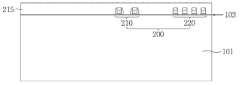
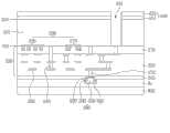
图1A和图1B是根据本发明构思的各个实施例的半导体器件1A和半导体器件1B的再分布结构的表面的概念布局。1A and 1B are conceptual layouts of surfaces of redistribution structures of a semiconductor device 1A and a
参考图1A和图1B,根据本发明构思的各个实施例的半导体器件1A和半导体器件1B中的每一个可以包括暴露的通孔结构4、互连结构5和布置在表面2上的焊盘6。表面2可以由绝缘材料覆盖,诸如氮化硅、氧化硅、聚酰亚胺、光敏聚酰亚胺、苯并环丁烯(BCB)或其它有机或无机聚合物。在其它附图中对通孔结构4、互连结构5和焊盘6进行更详细的描述。再参考图1A,通孔结构4可以以行或列的方式布置在表面2的中央。焊盘6可以布置在表面2上的各个位置处。互连结构5可以变化布置以电连接各通孔结构4或电连接通孔结构4和焊盘6。再参考图1B,通孔结构4可以以列布置在表面2的外部区域中。焊盘6可以布置在表面2上的各个位置处。互连结构5可以变化布置以电连接各通孔结构4或电连接通孔结构4和焊盘6。根据本发明构思的各个实施例的半导体器件1A和半导体器件1B中的每一个可以通过通孔结构4接收电源电压、参考电压、接地电压和各种电信号,并且使用再分布结构来将接收到的电源电压、参考电压、接地电压和各种电信号分布至布置在各个位置处的焊盘6。可替换地,根据本发明构思的各个实施例的半导体器件1A和半导体器件1B中的每一个可以通过焊盘6接收电源电压、参考电压、接地电压和各种电信号,并且使用再分布结构来将接收到的电源电压、参考电压、接地电压和各种电信号分布至布置在各个位置处的通孔结构4。Referring to FIGS. 1A and 1B , each of a semiconductor device 1A and a
图2A至图2S是根据本发明构思的各个实施例的通孔连接结构10A至通孔连接结构10S的概念纵截面图。2A to 2S are conceptual longitudinal sectional views of via
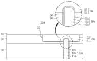
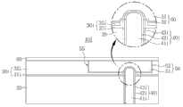
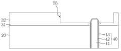
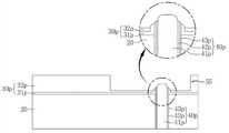
参考图2A,根据本发明构思的实施例的通孔连接结构10A可以包括具有槽55的绝缘层30、形成在槽55内并且具有突出的上部的通孔结构40a以及形成在槽55内的互连结构50。Referring to FIG. 2A , a via
绝缘层30可以形成在下层20上。下层20可以包括衬底或层间绝缘层。例如,下层20可以包括硅衬底。可替换地,例如,下层20可以包括包含氧化硅或氮化硅在内的层间绝缘层。An insulating
通孔结构40a可以包括通孔芯41a、通孔阻挡层42a和通孔衬垫43a。通孔结构40a可以在下层20的表面上从下层20的内部突出。通孔结构40a的侧表面的一部分可以暴露在下层20的表面上。例如,通孔芯41a、通孔阻挡层42a和通孔衬垫43a可以部分暴露在下层20上。The via structure 40a may include a via
通孔芯41a可以具有柱形。通孔芯41a可以包括金属,诸如铜(Cu)。The via
通孔阻挡层42a可以共形地覆盖通孔芯41a的侧表面和顶表面。通孔阻挡层42a可以包括阻挡金属(barrier metal),诸如钛(Ti)、氮化钛(TiN)、钽(Ta)、氮化钽(TaN)或氮化钨(WN)。通孔阻挡层42a可以形成为单层类型或多层类型。例如,通孔阻挡层42a可以包括多层阻挡金属层。The via barrier layer 42a may conformally cover side and top surfaces of the via
通孔衬垫43a可以共形地覆盖通孔芯41a的侧表面。例如,通孔衬垫43a可以覆盖通孔阻挡层42a的侧表面。通孔衬垫43a可以包括氧化硅(SiO2)、氮化硅(SiN)或其介电常数比氧化硅低的各种其它材料。The via
槽55可以形成在绝缘层30中。通孔结构40a的顶端和部分侧表面可以暴露在槽55内。例如,通孔结构40a的顶端和侧表面的一部分可以突出至槽55内。通孔阻挡层42a可以暴露在通孔结构40a的顶端和部分侧表面上,通孔结构40a的顶端和部分侧表面可以突出至槽55内。例如,在突出至槽55内的通孔结构40a的顶端部分和侧表面部分上可以不形成通孔衬垫43a。在槽55的底部表面上,绝缘层30的表面可以布置在与通孔衬垫43a的顶端实质上相同的水平或相似的水平处。绝缘层30可以覆盖通孔结构40a在槽55之下的侧表面。例如,埋入绝缘层30中的通孔结构40a的侧表面可以被绝缘层30包围。绝缘层30可以与通孔衬垫43a接触。
互连51和互连阻挡层52可以形成在槽55内。互连阻挡层52可以形成在槽55的内壁和底部表面以及暴露的通孔结构40a的表面上。互连阻挡层52可以沿着暴露在槽55内的通孔结构40a的轮廓共形地形成。互连51可以形成在槽55内的互连阻挡层52上以填充槽55。互连阻挡层52可以包括阻挡金属,诸如Ti、TiN、Ta、TaN或WN。同样,互连阻挡层52可以是单阻挡金属层或者是诸如两层或三层阻挡金属之类的阻挡金属复合层。互连51可以包括金属,诸如铜(Cu)。通孔阻挡层42a和互连阻挡层52中的每一个可以形成为单层类型或多层类型。The
可以在埋入绝缘层30中的通孔芯41a的侧表面上形成单阻挡层,例如仅通孔阻挡层42a,而可以在可突出至槽55内的通孔芯41a的侧表面上形成双阻挡层,例如通孔阻挡层42a和互连阻挡层52。因此,与在可以埋入下层20或绝缘层30中的通孔芯41a的侧表面上相比,在可以突出至槽55内的通孔芯41a的侧表面上可以形成较厚的阻挡层。A single barrier layer, such as only the via barrier layer 42a, may be formed on the side surface of the via
绝缘层30和互连结构50的顶部表面可以是平面。例如,绝缘层30和互连结构50的顶部表面可以处于同一水平。钝化层60可以直接形成在绝缘层30和互连结构50上。钝化层60可以包括氮化硅或聚酰亚胺。The top surfaces of the insulating
参考图2B,根据本发明构思的另一个实施例的通孔连接结构10B可以包括突出至槽55内的通孔结构40b。通孔结构40b可以包括通孔芯41b和通孔衬垫43b,通孔芯41b和通孔衬垫43b可以在绝缘层30的表面上突出。例如,通孔阻挡层42b可以覆盖通孔芯41b的全部顶部表面和侧表面,并且通孔衬垫43b可以覆盖通孔阻挡层42b的侧表面的一部分。通孔衬垫43b的顶端和一部分侧表面可以暴露在槽55内并且与互连阻挡层52接触。Referring to FIG. 2B , a via
参考图2C,根据本发明构思的另一个实施例的通孔连接结构10C可以包括突出至槽55内的通孔结构40c。通孔结构40c可以包括通孔芯41c、通孔阻挡层42c和通孔衬垫43c,通孔芯41c、通孔阻挡层42c和通孔衬垫43c可以在绝缘层30的表面上突出。例如,通孔阻挡层42c可以覆盖通孔芯41c的侧表面的一部分,并且通孔衬垫43c可以覆盖通孔阻挡层42c的侧表面。通孔阻挡层42c的顶端可以与通孔衬垫43c顶端表面相似。通孔阻挡层42c的顶端以及通孔衬垫43c的顶端和部分侧表面可以暴露在槽55内并且与互连阻挡层52接触。通孔芯41c可以与互连阻挡层52直接接触。Referring to FIG. 2C , a via connection structure 10C according to another embodiment of the inventive concept may include a via structure 40 c protruding into the
参考图2D,根据本发明构思的另一个实施例的通孔连接结构10D可以包括突出至槽55内的通孔结构40d。通孔结构40d可以包括通孔芯41d、通孔阻挡层42d和通孔衬垫43d,通孔芯41d、通孔阻挡层42d和通孔衬垫43d可以在绝缘层30的表面上突出。例如,通孔阻挡层42d可以覆盖通孔芯41d的侧表面的一部分,并且通孔衬垫43d可以覆盖通孔阻挡层42d的侧表面的一部分。通孔阻挡层42d的顶端可以布置在比通孔衬垫43d的顶端高的水平处。通孔阻挡层42d的顶端和部分侧表面以及通孔衬垫43d的顶端和部分侧表面可以暴露在槽55内并且与互连阻挡层52接触。Referring to FIG. 2D , a via connection structure 10D according to another embodiment of the inventive concept may include a via
参考图2E,根据本发明构思的另一个实施例的通孔连接结构10E可以包括突出至槽55内的通孔结构40e。通孔结构40e可以包括通孔芯41e和通孔阻挡层42e,通孔芯41e和通孔阻挡层42e可以在绝缘层30的表面上突出。例如,通孔芯41e的上部和/或部分侧表面可以不被通孔阻挡层42e覆盖而可以是暴露的。通孔芯41e的上部和/或部分侧表面可以与互连阻挡层52直接接触。通孔衬垫43e的顶端可以与绝缘层30的表面处于相同的水平或相似的水平处。Referring to FIG. 2E , a via
参考图2F,根据本发明构思的另一个实施例的通孔连接结构10F可以包括突出至槽55内的通孔结构40f。通孔结构40f可以包括通孔芯41f,通孔芯41f可以在绝缘层30的表面上突出。例如,通孔芯41f的上部和一部分侧表面可以不被通孔阻挡层42f覆盖而是暴露的。例如,仅通孔芯41f可以突出至槽55内。突出的通孔芯41f的上部和侧表面可以与互连阻挡层52直接接触。通孔阻挡层42f的顶端以及通孔衬垫43f的顶端可以与绝缘层30的表面处于相同的水平或相似的水平处。Referring to FIG. 2F , a via connection structure 10F according to another embodiment of the inventive concept may include a via structure 40 f protruding into the
参考图2G,根据本发明构思的另一个实施例的通孔连接结构10G可以包括下绝缘层31g和上绝缘层32g。同样,通孔连接结构10G可以包括可突出至槽55内的通孔芯41g和通孔阻挡层42g。下绝缘层31g可以形成在下层20上并且覆盖通孔结构40g的侧表面。上绝缘层32g可以形成在下绝缘层31g上并且具有槽55。上绝缘层32g可以与通孔结构40g的侧表面间隔开,并且不与通孔结构40g的侧表面接触。例如,下绝缘层31g可以插在上绝缘层32g和通孔结构40g之间。通孔阻挡层42g可以覆盖突出的通孔芯41g的顶部表面和侧表面。通孔阻挡层42g的顶部表面和侧表面可以与互连阻挡层52直接接触。在槽55内,通孔衬垫43g的顶部表面、下绝缘层31g和上绝缘层32g可以处于相同的水平或相似的水平。Referring to FIG. 2G , a via connection structure 10G according to another embodiment of the inventive concept may include a lower insulating layer 31 g and an upper insulating layer 32 g. Likewise, the via connection structure 10G may include a via core 41 g protruding into the
参考图2H,根据本发明构思的另一个实施例的通孔连接结构10H可以包括下绝缘层31h和上绝缘层32h,并且还包括突出至槽55内的通孔结构40h。通孔阻挡层42h可以覆盖通孔芯41h的顶部表面和侧表面。通孔衬垫43h可以覆盖突出的通孔阻挡层42h的侧表面的一部分。例如,通孔衬垫43h的顶端可以在槽55内从下绝缘层31h和上绝缘层32h的表面突出。通孔阻挡层42h的上部和一部分侧表面可以与互连阻挡层52直接接触。Referring to FIG. 2H , a via
参考图2I,根据本发明构思的另一个实施例的通孔连接结构10I可以包括下绝缘层31i和上绝缘层32i。通孔连接结构10I可以包括突出至槽55内的通孔结构40i和下绝缘层31i。下绝缘层31i的突出部可以覆盖通孔衬垫43i的侧表面。下绝缘层31i的突出部的顶端可以布置在与通孔衬垫43i的顶端相同的水平或相似的水平处。下绝缘层31i的侧表面的一部分可以与互连阻挡层52接触。Referring to FIG. 2I, a via connection structure 10I according to another embodiment of the inventive concept may include a lower insulating
参考图2J,根据本发明构思的另一个实施例的通孔连接结构10J可以包括下绝缘层31j和上绝缘层32j。通孔连接结构10J可以包括突出至槽55内的通孔结构40j和下绝缘层31j。下绝缘层31j的突出部可以覆盖通孔衬垫43j的侧表面的一部分。下绝缘层31j的侧表面的一部分可以与互连阻挡层52接触。Referring to FIG. 2J , a via connection structure 10J according to another embodiment of the inventive concept may include a lower insulating
参考图2K,根据本发明构思的另一个实施例的通孔连接结构10K可以包括下绝缘层31k和上绝缘层32k,并且还包括突出至槽55内的通孔芯41k。例如,通孔阻挡层42k、通孔衬垫43k、下绝缘层31k和上绝缘层32k的表面可以布置在相同的水平或相似的水平处。突出的通孔芯41k的顶部表面和侧表面可以与互连阻挡层52接触。Referring to FIG. 2K , a via
参考图2L,根据本发明构思的另一个实施例的通孔连接结构10L可以包括下绝缘层31l和上绝缘层32l,并且还包括突出至槽55内的通孔芯41l和通孔阻挡层42l。例如,通孔阻挡层42l可以覆盖通孔芯41l的侧表面的一部分。通孔衬垫43l、下绝缘层31l和上绝缘层32l的表面可以布置在相同的水平或相似的水平处。突出的通孔芯41l的顶部表面和部分侧表面可以与互连阻挡层52接触。Referring to FIG. 2L, a via
参考图2M,根据本发明构思的另一个实施例的通孔连接结构10M可以包括下绝缘层31m和上绝缘层32m,并且还包括可突出至槽55内的通孔结构40m。例如,通孔阻挡层42m可以覆盖通孔芯41m的侧表面的一部分。通孔衬垫43m可以覆盖通孔阻挡层42m的侧表面。通孔阻挡层42m的顶端可以布置在与通孔衬垫43m的顶端相同的水平或相似的水平处。突出的通孔芯41m的顶部表面和部分侧表面可以与互连阻挡层52接触。Referring to FIG. 2M , a via
参考图2N,根据本发明构思的另一个实施例的通孔连接结构10N可以包括下绝缘层31n和上绝缘层32n。通孔连接结构10N可以包括可突出至槽55内的通孔结构40n和下绝缘层31n。例如,通孔阻挡层42n可以覆盖通孔芯41n的侧表面的一部分。通孔衬垫43n可以覆盖通孔阻挡层42n的侧表面。突出的下绝缘层31n可以覆盖通孔衬垫43n的侧表面。通孔阻挡层42n的顶端、通孔衬垫43n的顶端以及下绝缘层31n的顶端可以在相同的水平或相似的水平处。突出的通孔芯41n的顶部表面和部分侧表面可以与互连阻挡层52接触。Referring to FIG. 2N , a via connection structure 10N according to another embodiment of the inventive concept may include a lower insulating
参考图2O,根据本发明构思的另一个实施例的通孔连接结构10O可以包括下绝缘层31o和上绝缘层32o,并且还包括可突出至槽55内的通孔结构40o。例如,通孔阻挡层42o可以覆盖通孔芯41o的侧表面的一部分。通孔衬垫43o可以覆盖通孔阻挡层42o的侧表面的一部分。突出的通孔芯41o的顶部表面和部分侧表面可以与互连阻挡层52接触。Referring to FIG. 2O , a via
参考图2P,根据本发明构思的另一个实施例的通孔连接结构10P可以包括下绝缘层31p和上绝缘层32p。通孔连接结构10P可以包括可突出至槽55内的通孔结构40p和下绝缘层31p。例如,通孔阻挡层42p可以覆盖通孔芯41p的侧表面的一部分。通孔衬垫43p可以覆盖通孔阻挡层42p的侧表面的一部分。突出的下绝缘层31p可以覆盖通孔衬垫43p的侧表面的一部分。突出的通孔芯41p的顶部表面和部分侧表面可以与互连阻挡层52接触。Referring to FIG. 2P, a via
参考图2Q,根据本发明构思的另一个实施例的通孔连接结构10Q可以包括下绝缘层31q和上绝缘层32q。通孔连接结构10Q可以包括可突出至槽55内的通孔结构40q和下绝缘层31q。例如,通孔阻挡层42q可以覆盖通孔芯41q的侧表面的一部分。通孔衬垫43q可以覆盖通孔阻挡层42q的侧表面。通孔衬垫43q的顶端和通孔阻挡层42q的顶端可以布置在相同的水平或相似的水平处。突出的下绝缘层31q可以覆盖通孔衬垫43q的侧表面的一部分。突出的通孔芯41q的顶部表面和部分侧表面可以与互连阻挡层52接触。Referring to FIG. 2Q , a via connection structure 10Q according to another embodiment of the inventive concept may include a lower insulating
参考图2R,根据本发明构思的另一个实施例的通孔连接结构10R可以包括可突出至槽55内的通孔结构40r。通孔结构40r可以包括可在绝缘层30的表面上突出的通孔芯41r和通孔阻挡层42r。例如,通孔芯41r的顶端和通孔阻挡层42r的顶端可以布置在相同的水平或相似的水平处(例如,具有共面的上表面)。通孔衬垫43r可以布置在与槽55的底部表面相同的水平或相似的水平处。绝缘层30可以被解释为上绝缘层32,而下层20可以被解释为下绝缘层31。Referring to FIG. 2R , a via
参考图2S,根据本发明构思的另一个实施例的通孔连接结构10S可以包括可突出至槽55内的通孔结构40s。通孔结构40s可以包括可在绝缘层30的表面上突出的通孔芯41s。例如,通孔芯41s的顶端和通孔阻挡层42s的顶端可以布置在相同的水平或相似的水平处。通孔衬垫43s可以部分或全部覆盖通孔阻挡层42s的侧表面。绝缘层30可以被解释为上绝缘层32,而下层20可以被解释为下绝缘层31。Referring to FIG. 2S , a via connection structure 10S according to another embodiment of the inventive concept may include a via structure 40s protruding into the
图2A至图2S中所示的全部通孔连接结构10A至通孔连接结构10S的组件的顶端都可以具有圆角。The top ends of the components of all the via
根据本发明构思的各个实施例的通孔连接结构10A至10S中的每一个可以包括使用大马士革工艺形成的互连结构50。因此,互连阻挡层52可以完全包围互连51的底部表面和侧表面。例如,当使用湿法蚀刻工艺或选择性蚀刻工艺来除去互连阻挡层52时,互连阻挡层52可能不完全包围互连51的底部或侧表面,因而引起物理的和/或电的不稳定。代替光刻和蚀刻工艺,可以使用CMP工艺来平面地形成根据本发明构思的各个实施例的通孔连接结构10A至10S,并且通孔结构40a至40s的节距(pitch)和互连结构50的节距可以变得更微小和更复杂。在根据本发明构思的各个实施例的通孔连接结构10A至10S中的每一个中,通孔结构40可以突出至互连结构50内。例如,通孔结构40可以插入互连结构50中。因此,通孔结构40a至40s与互连结构50之间的接触面积可以增加,使得通孔结构40a至40s与互连结构50之间的薄层电阻(sheet resistance)可以减小。而且,由于互连结构50可以由通孔结构40a至40s进行物理固定,因此可以防止由浮动现象引起的各组件的接触故障或分离。Each of the via
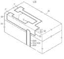
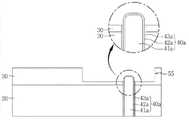
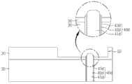
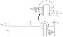
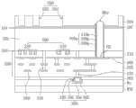
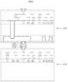
图3A至图3H是根据本发明构思的各个实施例的通孔连接结构11A至11H的概念纵截面的透视图。参考图3A至图3D,根据本发明构思的各个实施例的通孔连接结构11A至11D中的每一个可以具有:被配置为穿入下层20的通孔结构45a至45d中的相应的一个;在下层20上形成的绝缘层30;在绝缘层30中的、暴露通孔结构45a至45d中的相应的一个的顶端的槽55;以及被配置为填充槽55的互连结构50。槽55和互连结构50可以包括通孔区域V、焊盘区域P以及被配置为连接通孔区域V和焊盘区域P的互连区域L。通孔结构45a至45d中的每一个可以布置在通孔区域V内。通孔结构45a至45d中的每一个可以穿入下层20和绝缘层30,并且可以在槽55的底部表面上突出。互连阻挡层52可以共形地形成在槽55的侧表面和底部表面上和突出的通孔结构45a至45d中的每一个上。互连51可以形成在互连阻挡层52上以完全填充槽55。可以在焊盘区域P上形成I/O焊盘。稍后将描述I/O焊盘。因而,I/O焊盘和通孔结构45a至45d可以通过互连结构50电连接。通孔区域V和焊盘区域P可以比互连区域L具有更大的水平宽度。通孔区域V可以具有至少一个比焊盘区域P更大的水平宽度。3A to 3H are perspective views of conceptual longitudinal sections of via
参考图3E至图3H,根据本发明构思的各个实施例的通孔连接结构11E至11H中的每一个可以具有在下层20上形成的下绝缘层31。通孔结构45e至45h中的相应的一个可以配置为穿入下层20、下绝缘层31、使通孔结构45e至45h中的相应的一个的顶端暴露的槽55、以及被配置为填充槽55的互连结构50。可以在下绝缘层31上形成上绝缘层32。上绝缘层32可以不与通孔结构45e至45h中的每一个接触。下绝缘层31可以插入在上绝缘层32和通孔结构45e至45h中的每一个之间。下绝缘层31的顶端可以与互连阻挡层52接触。Referring to FIGS. 3E to 3H , each of the via
图3A至图3H中所示的全部通孔结构45a至45h的组件的顶端都可以具有圆角。图3A至图3H中所示的全部通孔结构45a至45h都可以分别具有通孔芯46a至46h、通孔阻挡层47a至47h以及通孔衬垫48a至48h。通孔芯46a至46h、通孔阻挡层47a至47h以及通孔衬垫48a至48h可以分别由如2A至图2S中所示的各个通孔结构40a至40s的通孔芯41a至41s、通孔阻挡层42a至42s以及通孔衬垫43a至43s来替换。The top ends of the components of all the via structures 45 a to 45 h shown in FIGS. 3A to 3H may have rounded corners. All via structures 45 a to 45 h shown in FIGS. 3A to 3H may have via
图4A和图4B是示出了形成根据本发明构思的各个实施例的通孔连接结构10A至10S的方法的流程图;并且图5A至图5G以及图6A至图6C是示出了形成根据本发明构思的各个实施例的通孔连接结构10A至10S的方法的纵截面图。4A and 4B are flowcharts illustrating methods of forming via
参考图4A和图5A,形成根据本发明构思的实施例的通孔连接结构10A至10F的方法可以包括在下层20中形成通孔结构40(操作S10)。通孔结构40可以埋入下层20中。通孔结构40可以包括通孔芯41、被配置为包围通孔芯41的表面的通孔阻挡层42、以及被配置为包围通孔阻挡层42的表面的通孔衬垫43。将参考本公开的其它附图来详细描述形成通孔结构40的方法。Referring to FIGS. 4A and 5A , a method of forming via
参考图4A和图5B,形成根据本发明构思的本实施例的通孔连接结构10A至10F的方法可以包括地毯式地(blanketly)除去下层20的上部以使通孔结构40的顶部表面和部分侧表面暴露(操作S20)。下层20的顶部表面可以从初始表面S1降低至最终表面S2。通孔衬垫43可以暴露在从降低后的下层20向上突出的通孔结构40的表面上。可替换地,可以暴露通孔阻挡层42。除去下层20的上部可以包括执行研磨工艺、湿法蚀刻工艺和/或干法蚀刻工艺。Referring to FIGS. 4A and 5B , the method of forming the via
参考图4A和图5C,形成根据本发明构思的本实施例的通孔连接结构10A至10F的方法可以包括在下层20上形成绝缘层30以覆盖通孔结构40(操作S30)。绝缘层30可以包括氧化硅或氮化硅。Referring to FIGS. 4A and 5C , the method of forming the via
参考图4A和图5D,形成根据本发明构思的本实施例的通孔连接结构10A至10F的方法可以包括在绝缘层30中形成槽55以使通孔结构40的顶部表面和侧表面暴露(操作S40)。例如,通孔结构40可以突出至槽55内。在此工艺期间,可以将暴露在突出至槽55内的通孔结构40的表面上的通孔衬垫43除去。Referring to FIGS. 4A and 5D , the method of forming the via
参考图4A和图5E,形成根据本发明构思的本实施例的通孔连接结构10A至10F的方法可以包括在槽55内形成互连阻挡材料层52a(操作S50)。互连阻挡材料层52a可以共形地形成在槽55的内壁和底部表面上以及通孔结构40的暴露表面上。互连阻挡材料层52a还可以形成在绝缘层30的顶部表面上。Referring to FIGS. 4A and 5E , the method of forming the via
参考图4A和图5F,形成根据本发明构思的本实施例的通孔连接结构10A至10F的方法可以包括在槽55内形成互连材料层51a(操作S60)。互连材料层51a可以形成在互连阻挡材料层52a上以完全填充槽55。例如,形成互连材料层51a可以包括在互连阻挡材料层52a上形成种子层以及执行电镀工艺。互连材料层51a还可以形成在绝缘层30的顶部表面上。Referring to FIGS. 4A and 5F , the method of forming the via
参考图4A和图5G,形成根据本发明构思的本实施例的通孔连接结构10A至10F的方法可以包括形成互连结构50以填充槽55(操作S70)。形成互连结构50可以包括将在绝缘层30上形成的互连材料层51a的一部分以及互连阻挡材料层52a的一部分除去。将互连材料层51a的一部分以及互连阻挡材料层52a的一部分除去可以包括执行化学机械抛光(CMP)工艺和/或湿法蚀刻工艺。归功于该工艺,可以形成具有互连51和互连阻挡层52的互连结构50。随后,可以在绝缘层30和互连结构50上形成钝化层60,从而完成了图2A所示的通孔连接结构10A的形成(操作S80)。Referring to FIGS. 4A and 5G , the method of forming the via
参考图4B和图6A,形成根据本发明构思的实施例的通孔连接结构10G至10S的方法可以包括执行参考图5A和图5B描述的工艺(操作S10和S20)以及在下层20和突出的通孔结构40上形成下绝缘层31(操作S25)。下绝缘层31可以包括氧化硅。Referring to FIGS. 4B and 6A , the method of forming the via connection structures 10G to 10S according to an embodiment of the inventive concept may include performing the process described with reference to FIGS. 5A and 5B (operations S10 and S20 ) and forming The lower insulating
参考图4B和图6B,形成根据本发明构思的本实施例的通孔连接结构10G至10S的方法可以包括在下绝缘层31上形成上绝缘层32(操作S35)。上绝缘层32可以形成为掩埋突出的通孔结构40。上绝缘层32可以包括氮化硅。Referring to FIGS. 4B and 6B , the method of forming the via connection structures 10G to 10S according to the present embodiment of the inventive concept may include forming the upper insulating
参考图4B和图6C,形成根据本发明构思的本实施例的通孔连接结构10G至10S的方法可以包括在上绝缘层32中形成槽55以使通孔结构40的顶部表面和侧表面暴露(操作S42)。在此工艺期间,可以除去在突出的通孔结构40的表面上形成的下绝缘层31和通孔衬垫43。例如,可以暴露通孔阻挡层42。同样,下绝缘层31的一部分可以暴露在槽55的底部表面上。此后,形成根据本发明构思的本实施例的通孔连接结构10G至10S的方法可以还包括执行参考图5E至图5G描述的工艺(操作S50至S80),从而完成图2G所示的通孔连接结构10G的形成。Referring to FIGS. 4B and 6C , the method of forming the via connection structures 10G to 10S according to the present embodiment of the inventive concept may include forming a
图7A至图7Q是具有各种形状的通孔结构40a至40q的概念纵截面图,在形成根据本发明构思的各个实施例的通孔连接结构10A至10Q的方法中,通孔结构40a至40q暴露在槽55内。7A to 7Q are conceptual longitudinal cross-sectional views of via hole structures 40a to 40q having various shapes, which are used in methods of forming via
参考图7A,形成根据本发明构思的实施例的通孔连接结构10A的方法可以包括将突出至槽55内的通孔结构40a的通孔衬垫43a除去。通孔阻挡层42a可以覆盖通孔芯41a的整个表面。Referring to FIG. 7A , a method of forming a via
参考图7B,形成根据本发明构思的实施例的通孔连接结构10B的方法可以包括形成突出至槽55内的通孔结构40b的通孔衬垫43b,以使通孔阻挡层42b的顶端的表面暴露并且部分或全部覆盖通孔阻挡层42b的侧表面。通孔阻挡层42b可以覆盖通孔芯41b的整个表面。Referring to FIG. 7B , a method of forming a via
参考图7C,形成根据本发明构思的实施例的通孔连接结构10C的方法可以包括:形成突出至槽55内的通孔结构40c的通孔阻挡层42c,以使通孔芯41c的顶端的表面暴露并且部分或全部覆盖通孔芯41c的侧表面;以及形成通孔衬垫43c,以使突出至槽55内的通孔阻挡层42c的顶端的表面暴露并且全部覆盖通孔阻挡层42c的侧表面。Referring to FIG. 7C , a method of forming a via connection structure 10C according to an embodiment of the inventive concept may include: forming a via barrier layer 42c protruding into the via structure 40c in the
参考图7D,形成根据本发明构思的实施例的通孔连接结构10D的方法可以包括:形成突出至槽55内的通孔结构40d的通孔阻挡层42d,以使通孔芯41d的顶端的表面暴露并且部分或全部覆盖通孔芯41d的侧表面;以及形成通孔衬垫43d,以使突出至槽55内的通孔阻挡层42d的顶端的表面暴露并且部分覆盖通孔阻挡层42d的侧表面。Referring to FIG. 7D , a method of forming a via connection structure 10D according to an embodiment of the inventive concept may include forming a via
参考图7E,形成根据本发明构思的实施例的通孔连接结构10E的方法可以包括:形成突出至槽55内的通孔结构40e的通孔阻挡层42e,以使通孔芯41e的顶端的表面暴露并且部分或全部覆盖通孔芯41e的侧表面;以及形成通孔衬垫43e,以使突出至槽55内的通孔阻挡层42e的顶端表面和侧表面暴露。例如,该方法可以包括形成通孔衬垫43e,使得通孔衬垫43e的顶端布置在与槽55的底部表面相同的水平或相似的水平处。Referring to FIG. 7E , a method of forming a via
参考图7F,形成根据本发明构思的实施例的通孔连接结构10F的方法可以包括将突出至槽55内的通孔结构40f的通孔阻挡层42f和通孔衬垫43f除去,以使通孔芯41f的顶端表面和侧表面全部暴露。Referring to FIG. 7F , a method of forming a via connection structure 10F according to an embodiment of the inventive concept may include removing the via barrier layer 42f and the via
参考图7G,形成根据本发明构思的实施例的通孔连接结构10G的方法可以包括形成下绝缘层31g和上绝缘层32g,并且使在槽55内的下绝缘层31g的顶端的一部分暴露。通孔芯41g和通孔阻挡层42g可以突出至槽55内。下绝缘层31g可以包围通孔结构40g并且与通孔衬垫43g的侧表面接触。上绝缘层32g可以与通孔衬垫43g隔离开并且不与通孔衬垫43g接触。通孔阻挡层42g可以覆盖突出的通孔芯41g的顶部表面和侧表面。通孔阻挡层42g的顶部表面和侧表面可以与互连阻挡层52直接接触。在槽55内,通孔衬垫43g的顶部表面、下绝缘层31g和上绝缘层32g可以在相同的水平或相似的水平处。Referring to FIG. 7G , a method of forming a via connection structure 10G according to an embodiment of the inventive concept may include forming a lower insulating layer 31g and an upper insulating layer 32g and exposing a portion of a top end of the lower insulating layer 31g within the
参考图7H,形成根据本发明构思的实施例的通孔连接结构10H的方法可以包括形成下绝缘层31h和上绝缘层32h,并且使通孔衬垫43h的顶端突出至槽55内。Referring to FIG. 7H , a method of forming a via
参考图7I,形成根据本发明构思的实施例的通孔连接结构10I的方法可以包括形成下绝缘层31i和上绝缘层32i,并且使通孔衬垫43i的顶端以及下绝缘层31i的顶端突出至槽55内。通孔衬垫43i的顶端以及下绝缘层31i的顶端可以布置在相同的水平或相似的水平处。Referring to FIG. 7I , a method of forming a via connection structure 10I according to an embodiment of the inventive concept may include forming a lower insulating
参考图7J,形成根据本发明构思的实施例的通孔连接结构10J的方法可以包括形成下绝缘层31j和上绝缘层32j,并且使通孔衬垫43j的顶端以及下绝缘层31j的顶端突出至槽55内。通孔衬垫43j的顶端可以布置在比下绝缘层31j的顶端高的水平处。Referring to FIG. 7J , a method of forming a via connection structure 10J according to an embodiment of the inventive concept may include forming a lower insulating
参考图7K,形成根据本发明构思的实施例的通孔连接结构10K的方法可以包括形成下绝缘层31k和上绝缘层32k,并且使通孔芯41k突出至槽55内。通孔阻挡层42k可以部分覆盖通孔芯41k的侧表面。通孔阻挡层42k的顶端、通孔衬垫43k的顶端、下绝缘层31k的顶端和上绝缘层32k的顶端可以布置在相同的水平或相似的水平处。Referring to FIG. 7K , a method of forming a via
参考图7L,形成根据本发明构思的实施例的通孔连接结构10L的方法可以包括形成下绝缘层31l和上绝缘层32l,并且使通孔芯41l突出至槽55内。通孔阻挡层42l可以全部或部分覆盖通孔芯41l的侧表面。通孔阻挡层42l可以突出至槽55内。通孔衬垫43l的顶端、下绝缘层31l的顶端和上绝缘层32l的顶端可以布置在相同的水平或相似的水平处。Referring to FIG. 7L , a method of forming a via
参考图7M,形成根据本发明构思的实施例的通孔连接结构10M的方法可以包括形成下绝缘层31m和上绝缘层32m,并且使通孔芯41m突出至槽55内。通孔阻挡层42m可以突出至槽55内并且部分或全部覆盖通孔芯41m的侧表面。通孔衬垫43m可以突出至槽55内并且部分或全部覆盖通孔阻挡层42m的侧表面。Referring to FIG. 7M , a method of forming a via
参考图7N,形成根据本发明构思的实施例的通孔连接结构10N的方法可以包括形成下绝缘层31n和上绝缘层32n,并且使通孔芯41n突出至槽55内。通孔阻挡层42n可以突出至槽55内并且部分或全部覆盖通孔芯41n的侧表面。通孔衬垫43n可以突出至槽55内并且全部覆盖通孔阻挡层42n的侧表面。下绝缘层31n的一部分可以突出至槽55内并且全部覆盖通孔衬垫43n的侧表面。Referring to FIG. 7N , a method of forming a via connection structure 10N according to an embodiment of the inventive concept may include forming a lower insulating
参考图7O,形成根据本发明构思的实施例的通孔连接结构10O的方法可以包括形成下绝缘层31o和上绝缘层32o,并且使通孔芯41o突出至槽55内。通孔阻挡层42o可以突出至槽55内并且部分或全部覆盖通孔芯41o的侧表面。通孔衬垫43o可以突出至槽55内并且部分或全部覆盖通孔阻挡层42o的侧表面。下绝缘层31o的顶部表面可以布置在与上绝缘层32o的表面相同的水平或相似的水平处。Referring to FIG. 7O , a method of forming a via
参考图7P,形成根据本发明构思的实施例的通孔连接结构10P的方法可以包括形成下绝缘层31p和上绝缘层32p,并且使通孔芯41p突出至槽55内。通孔阻挡层42p可以突出至槽55内并且部分或全部覆盖通孔芯41p的侧表面。通孔衬垫43p可以突出至槽55内并且部分或全部覆盖通孔阻挡层42p的侧表面。下绝缘层31p的一部分可以突出至槽55内并且部分或全部覆盖通孔衬垫43p的侧表面。Referring to FIG. 7P , a method of forming a via
参考图7Q,形成根据本发明构思的实施例的通孔连接结构10Q的方法可以包括形成下绝缘层31q和上绝缘层32q,并且使通孔芯41q突出至槽55内。通孔阻挡层42q可以突出至槽55内并且部分或全部覆盖通孔芯41q的侧表面。通孔衬垫43q可以突出至槽55内并且全部覆盖通孔阻挡层42q的侧表面。通孔阻挡层42q的顶端和通孔衬垫43q的顶端可以布置在相同的水平或相似的水平处。下绝缘层31q的一部分可以突出至槽55内并且部分或全部覆盖通孔衬垫43q的侧表面。Referring to FIG. 7Q , a method of forming a via connection structure 10Q according to an embodiment of the inventive concept may include forming a lower insulating
形成根据本发明构思的各个实施例的各通孔连接结构的各方法可以包括使用大马士革工艺来形成互连结构50。因此,互连阻挡层52可以完全包围互连51的底部表面和侧表面。例如,当使用湿法蚀刻工艺或选择性蚀刻工艺来除去互连阻挡层52时,互连阻挡层52可能不完全包围互连51的底部或侧表面,因而引起物理的和/或电的不稳定。代替光刻和蚀刻工艺,形成根据本发明构思的各个实施例的各通孔连接结构的各方法可以采用CMP工艺。因而,通孔结构40a至40s的节距和互连结构50的节距可以变得更微小和更复杂。在形成根据本发明构思的各个实施例的各通孔连接结构的各方法中的每一个方法中,通孔结构40a至40s可以突出至互连结构50内。例如,通孔结构40a至40s可以插入互连结构50中。因此,通孔结构40a至40s与互连结构50之间的接触面积可以增加,使得通孔结构40a至40s与互连结构50之间的薄层电阻可以减小。而且,由于互连结构50可以由通孔结构40a至40s进行物理固定,因此可以防止由浮动现象引起的各组件的接触故障或分离。Methods of forming via connection structures according to various embodiments of the inventive concept may include forming the
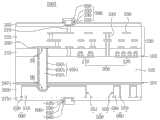
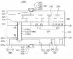
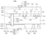
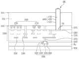
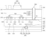
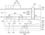
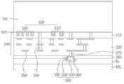
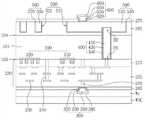
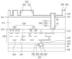
图8A至图8S是根据本发明构思的各个实施例的半导体器件100A至100S的概念纵截面图。参考图8A,根据本发明构思的实施例的半导体器件100A可以包括:在衬底101的正面103上形成的内部电路230和正面输入/输出(I/O)焊盘300;在衬底101中形成的硅通孔(TSV)结构400a;以及在衬底101的背面104上形成的再分布结构500和背面I/O焊盘600。8A to 8S are conceptual longitudinal cross-sectional views of
衬底101可以是硅晶圆。例如,衬底101可以包括单晶硅晶圆、包括碳化硅(SiC)层或硅锗(SiGe)层的硅晶圆、或者包括绝缘层的绝缘体上硅(SOI)晶圆。在本实施例中,假设衬底101是单晶硅晶圆。The
包括单元器件200的内部电路230可以形成在衬底101的正面103上。例如,单元器件200可以包括金属氧化物半导体(MOS)晶体管210和单元图案(cell pattern)220。MOS晶体管210可以包括互补MOS(CMOS)逻辑电路。单元图案220可以包括闪存串结构。例如,单元图案220可以包括多个闪存单元。可替换地,当半导体器件100A为逻辑器件时,单元图案220可以包括各种单元晶体管。An
内部电路230可以包括多个导电的内部通孔240和多层的导电的内部互连250。内部通孔240可以在垂直方向上连接在衬底101和内部互连250之间或者连接在各内部互连250之间,并且传送电信号。内部互连250可以在水平方向上传送电信号。内部电路230可以包括导电材料,诸如掺杂硅、金属、金属硅化物、金属合金或金属化合物。内部电路230可以包括正面I/O焊盘通孔插头270。正面I/O焊盘通孔插头270可以将最上面的内部互连250的一部分与正面I/O焊盘300电连接。正面I/O焊盘通孔插头270可以包括金属,诸如铜(Cu)、铝(Al)或钨(W)。The
单元器件200可以由第一层间绝缘层215覆盖。虽然将第一层间绝缘层215形成为多层类型,但是为了简洁示出了具有单层结构的第一层间绝缘层215。第一层间绝缘层215可以包括氧化硅或氮化硅。例如,当第一层间绝缘层215是单层时,第一层间绝缘层215可以包括氧化硅。内部电路230可以由第二层间绝缘层225覆盖。虽然可以将第二层间绝缘层225形成为多层类型,但是为了简洁示出了具有单层结构的第二层间绝缘层225。第二层间绝缘层225可以包括氧化硅或氮化硅。The
可以在第二层间绝缘层225上形成正面钝化层265。正面钝化层265可以包括氧化硅、氮化硅或聚酰亚胺。正面钝化层265可以具有正面I/O焊盘开口310,正面I/O焊盘开口310使正面I/O焊盘通孔插头270的上部暴露。A
正面I/O焊盘300可以形成在正面I/O焊盘开口310内和在正面钝化层265的表面上。正面钝化层265可以包围正面I/O焊盘300的侧表面的一部分。例如,正面I/O焊盘300可以具有反向阶梯,而正面钝化层265可以布置在正面I/O焊盘300的反向阶梯的底部表面之下。正面I/O焊盘300可以包括正面I/O焊盘阻挡层320、正面I/O焊盘种子层330、正面I/O焊盘金属层350、和/或正面I/O焊盘覆盖层360。正面I/O焊盘阻挡层320可以包括阻挡金属。例如,正面I/O焊盘阻挡层320可以包括钛(Ti)、氮化钛(TiN)、钽(Ta)、氮化钽(TaN)、钛钨(TiW)、或其它难熔金属。正面I/O焊盘种子层330可以包括种子金属,诸如铜(Cu)、钌(Ru)、镍(Ni)或钨(W)。正面I/O焊盘金属层350可以包括金属,诸如铜或镍。正面I/O焊盘覆盖层360可以包括金(Au)、银(Ag)或镍(Ni)。正面I/O焊盘阻挡层320可以是多层类型。Front I/
可以在衬底101的正面103的上方,例如在第一层间绝缘层215上,形成硅通孔(TSV)焊盘260。TSV焊盘260可以与内部电路230的一些电连接。TSV焊盘260可以包括金属、金属硅化物或金属合金。TSV焊盘260可以是多层类型。例如,TSV焊盘260可以包括用作阻挡层的金属层和用作焊盘的金属层。例如,TSV焊盘260可以包括:在与TSV结构400a接触的部分上以相对小的厚度形成的TSV焊盘阻挡层;以及在TSV焊盘阻挡层上作为单层类型或多层类型形成的TSV焊盘金属层。例如,TSV焊盘阻挡层可以包括由Ti、TiN、Ta、TaN或WN制成的金属或金属硅化物。TSV焊盘金属层可以包括诸如钨(W)、铝(Al)或铜(Cu)之类的金属或金属硅化物。A through silicon via (TSV)
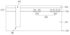
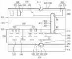
TSV结构400a可以形成为穿透衬底101。TSV结构400a可以包括面向衬底101的正面103的正面端FE以及面向衬底101的背面104的背面端BE。例如,TSV结构400a的正面端FE可以布置为接近于衬底101的正面103,并且TSV结构400a的背面端BE可以布置为接近于衬底101的背面104。The
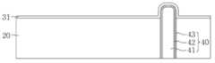
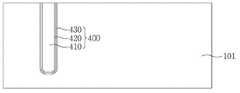
TSV结构400a可以包括TSV芯410a、TSV阻挡层420a和TSV衬垫430a。TSV芯410a可以形成为柱形,并且TSV芯410a的侧表面可以由TSV阻挡层420a和TSV衬垫430a包围。例如,TSV芯410a可以包括金属,诸如铜(Cu)。TSV阻挡层420a可以包括阻挡金属,诸如Ti、TiN、Ta、TaN或TiW。TSV阻挡层420a可以形成为单层类型或多层类型。TSV衬垫430a可以包括绝缘材料,诸如氧化硅。The
TSV结构400a的正面端FE可以与TSV焊盘260接触。TSV芯410a可以在TSV结构400a的正面端FE暴露,并且与TSV焊盘260直接接触。The front end FE of the
TSV结构400a的背面端BE可以从衬底101的背面104的表面突出。例如,TSV结构400a的背面端BE的顶部表面和背面端BE的侧表面的一部分可以从衬底101的背面104突出。所示出的是TSV结构400a的背面端BE从衬底101的背面104向下突出。TSV结构400a的背面端BE的顶部表面和背面端BE的侧表面的该部分可以由TSV阻挡层420a覆盖。TSV衬垫430a可以不形成在TSV结构400a的背面端BE的顶部表面和TSV结构400a的侧表面的部分上。例如,TSV阻挡层420a可以与再分布结构500直接接触。The backside end BE of the
可以在衬底101的背面104上形成背面绝缘层285a。背面绝缘层285a可以包括氧化硅或氮化硅。背面绝缘层285a可以包括槽550。槽550可以包括再分布槽551和对准标记(alignment key)槽552。A
可以在再分布槽551内形成再分布结构500。再分布结构500可以包括再分布阻挡层520和再分布互连510。The
TSV结构400a的背面端BE可以突出至再分布槽551内。再分布阻挡层520可以形成在TSV结构400a的背面端BE的暴露表面上。例如,再分布阻挡层520可以共形地形成在可突出至再分布槽551内的TSV结构400a的背面端BE的顶部表面和侧表面上。TSV阻挡层420a可以在可突出至再分布槽551内的TSV结构400a的背面端BE上暴露,并且与再分布阻挡层520直接接触。再分布阻挡层520可以沿着可突出至再分布槽551内的TSV结构400a的轮廓共形地形成。背面绝缘层285a可以包围TSV结构400a的侧表面的一部分。例如,在再分布槽551下面形成的背面绝缘层285a可以包围TSV结构400a的侧表面的该部分。The back end BE of the
当被埋入衬底101或背面绝缘层285a中的TSV结构400a的侧表面由具有第一厚度的单阻挡层(例如,TSV阻挡层420a)包围时,突出至再分布槽551内的TSV结构400a的表面可以具有第二厚度的多层阻挡层(例如,TSV阻挡层420a和再分布阻挡层520)。第二厚度可以大于第一厚度。例如,TSV结构400a的可不与再分布结构500接触的部分可以具有相对薄的阻挡层,而TSV结构400a的可与再分布结构500接触的部分可以具有相对厚的阻挡层。When the side surface of the
可以在对准标记槽552内形成对准标记结构560。对准标记结构560可以包括对准标记阻挡层570和对准标记图案580。对准标记槽552可以具有与再分布槽551相同的深度。可以以与再分布阻挡层520相同的厚度、相同的材料来形成对准标记阻挡层570。可以以与再分布互连510相同的材料来形成对准标记图案580。
可以在再分布结构500和对准标记结构560上形成背面钝化层275a。背面钝化层275a可以包括氧化硅、氮化硅或聚酰亚胺。背面钝化层275a可以具有使再分布互连510的一部分暴露的背面I/O焊盘开口610。A
可以在背面I/O焊盘开口610内和在背面钝化层275a的表面上形成背面I/O焊盘600。背面I/O焊盘600可以包括背面I/O焊盘阻挡层620、背面I/O焊盘种子层630、背面I/O焊盘金属层650、和/或背面I/O焊盘覆盖层660。背面I/O焊盘阻挡层620可以包括阻挡金属。例如,背面I/O焊盘阻挡层620可以包括Ti、TiN、Ta、TaN、TiW或其它难熔金属。背面I/O焊盘阻挡层620可以形成为单层类型或多层类型。背面I/O焊盘种子层630可以包括种子金属,诸如铜(Cu)、钌(Ru)、镍或钨(W)。背面I/O焊盘金属层650可以包括金属,诸如铜或镍。背面I/O焊盘覆盖层660可以包括金(Au)、银(Ag)或镍(Ni)。例如,正面I/O焊盘300和背面I/O焊盘600可以在垂直方向上对准。Back I/
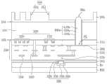
参考图8B,根据本发明构思的实施例的半导体器件100B可以包括可突出至再分布槽551内的TSV结构400b。TSV结构400b可以包括可突出至再分布槽551内的TSV芯410b和TSV阻挡层420b。例如,TSV阻挡层420b可以覆盖TSV芯410b的全部顶部表面和侧表面,并且TSV衬垫430b可以覆盖TSV阻挡层420b的侧表面的一部分。TSV衬垫430b的顶端和部分侧表面可以暴露在再分布槽551内,并且与再分布阻挡层520接触。Referring to FIG. 8B , a
参考图8C,根据本发明构思的实施例的半导体器件100C可以包括可突出至再分布槽551内的TSV结构400c。TSV结构400c可以包括可突出至再分布槽551内的TSV芯410c、TSV阻挡层420c和TSV衬垫430c。例如,TSV阻挡层420c可以覆盖TSV芯410c的侧表面的一部分,而TSV衬垫430c可以覆盖TSV阻挡层420c的侧表面。TSV阻挡层420c的顶端可以与TSV衬垫430c的顶端表面处于相似的水平处。TSV阻挡层420c的顶端以及TSV衬垫430c的顶端和部分侧表面可以暴露在再分布槽551内,并且与再分布阻挡层520接触。TSV芯410c可以与再分布阻挡层520直接接触。Referring to FIG. 8C , a semiconductor device 100C according to an embodiment of the inventive concept may include a
参考图8D,根据本发明构思的实施例的半导体器件100D可以包括可突出至再分布槽551内的TSV结构400d。TSV结构400d可以包括可突出至再分布槽551内的TSV芯410d、TSV阻挡层420d和TSV衬垫430d。例如,TSV阻挡层420d可以覆盖TSV芯410d的侧表面的一部分,并且TSV衬垫430d可以覆盖TSV阻挡层420d的侧表面的一部分。TSV阻挡层420d的顶端可以处于比TSV衬垫430d的顶端高的水平处。TSV阻挡层420d的顶端和部分侧表面以及TSV衬垫430d的顶端和部分侧表面可以暴露在再分布槽551内,并且与再分布阻挡层520接触。Referring to FIG. 8D , a
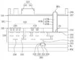
参考图8E,根据本发明构思的实施例的半导体器件100E可以包括可突出至再分布槽551内的TSV结构400e。TSV结构400e可以包括可突出至再分布槽551内的TSV芯410e和TSV阻挡层420e。例如,TSV芯410e的上部和/或部分侧表面可以不被TSV阻挡层420e覆盖而是暴露着的。TSV芯410e的上部和/或部分侧表面可以与再分布阻挡层520直接接触。TSV衬垫430e的顶端可以处在与背面绝缘层285e的表面相同的水平或相似的水平处。Referring to FIG. 8E , a
参考图8F,根据本发明构思的实施例的半导体器件100F可以包括可突出至再分布槽551内的TSV结构400f。TSV结构400f可以包括可突出至再分布槽551内的TSV芯410f。例如,TSV芯410f的上部和部分侧表面可以不被TSV阻挡层420f覆盖而是暴露着的。例如,只有TSV芯410f可突出至再分布槽551内。突出的TSV芯410f的上部和侧表面可以与再分布阻挡层520直接接触。TSV阻挡层420f的顶端和TSV衬垫430f的顶端可以处在与背面绝缘层285f的表面相同的水平或相似的水平处。Referring to FIG. 8F , a
参考图8G,根据本发明构思的实施例的半导体器件100G可以包括:在衬底101的背面侧104上形成的下背面绝缘层287g;在下背面绝缘层287g上形成的并且具有槽550的上背面绝缘层289g;以及可突出至再分布槽551内的TSV芯410g和TSV阻挡层420g。下背面绝缘层287g可以与TSV结构400g的侧表面接触。下背面绝缘层287g的、可与TSV结构400g的背面端BE接近的部分可以与再分布阻挡层520接触。下背面绝缘层287g可以形成在衬底101的背面104上并且覆盖TSV结构400g的侧表面的一部分。上背面绝缘层289g可以形成在下背面绝缘层287g上并且具有槽550。上背面绝缘层289g可以不与TSV结构400g的侧表面接触并且与TSV结构400g的侧表面隔离开。例如,下背面绝缘层287g可以插入在上背面绝缘层289g和TSV结构400g之间。TSV阻挡层420g可以覆盖突出的TSV芯410g的顶部表面和侧表面。TSV阻挡层420g的顶部表面和侧表面可以与再分布阻挡层520直接接触。在再分布槽551内,TSV衬垫430g的顶部表面、下背面绝缘层287g的顶部表面和上背面绝缘层289g的顶部表面可以处在相同的水平或相似的水平处。Referring to FIG. 8G , a
参考图8H,根据本发明构思的实施例的半导体器件100H可以包括下背面绝缘层287h和上背面绝缘层289h,并且还包括突出至再分布槽551内的TSV结构400h。TSV阻挡层420h可以覆盖TSV芯410h的顶部表面和侧表面。TSV衬垫430h可以覆盖突出的TSV阻挡层420h的侧表面的一部分。例如,TSV衬垫430h的顶端可以在再分布槽551内从下背面绝缘层287h和上背面绝缘层289h的表面突出。TSV阻挡层420h的上部和部分侧表面可以与再分布阻挡层520直接接触。Referring to FIG. 8H , a
参考图8I,根据本发明构思的实施例的半导体器件100I可以包括下背面绝缘层287i和上背面绝缘层289i。半导体器件100I可以包括可突出至再分布槽551内的TSV结构400i和下背面绝缘层287i。下背面绝缘层287i的突出部可以覆盖TSV衬垫430i的侧表面的一部分。下背面绝缘层287i的突出部的顶端以及TSV衬垫430i的顶端可以布置在相同的水平或相似的水平处。下背面绝缘层287i的侧表面的一部分可以与再分布阻挡层520接触。Referring to FIG. 8I, a semiconductor device 100I according to an embodiment of the inventive concept may include a lower
参考图8J,根据本发明构思的实施例的半导体器件100J可以包括下背面绝缘层287j和上背面绝缘层289j。半导体器件100J可以包括可突出至再分布槽551内的TSV结构400j和下背面绝缘层287j。下背面绝缘层287j的突出部可以覆盖TSV衬垫430j的侧表面的一部分。下背面绝缘层287j的侧表面的一部分可以与再分布阻挡层520接触。Referring to FIG. 8J , a
参考图8K,根据本发明构思的实施例的半导体器件100K可以包括下背面绝缘层287k和上背面绝缘层289k,并且还包括突出至再分布槽551内的TSV芯410k。例如,TSV阻挡层420k的表面、TSV衬垫430k的表面、下背面绝缘层287k的表面和上背面绝缘层289k的表面可以布置在相同的水平或相似的水平处。突出的TSV芯410k的顶部表面和侧表面可以与再分布阻挡层520接触。Referring to FIG. 8K , a
参考图8L,根据本发明构思的实施例的半导体器件100L可以包括下背面绝缘层287l和上背面绝缘层289l,并且还包括可突出至再分布槽551内的TSV芯410l和TSV阻挡层420l。例如,TSV阻挡层420l可以覆盖TSV芯410l的侧表面的一部分。TSV衬垫430l的表面、下背面绝缘层287l的表面和上背面绝缘层289l的表面可以布置在相同的水平或相似的水平处。突出的TSV芯410l的顶部表面和部分侧表面可以与再分布阻挡层520接触。Referring to FIG. 8L , a semiconductor device 100L according to an embodiment of the inventive concept may include a lower backside insulating layer 287l and an upper backside insulating layer 289l, and further include a TSV core 410l and a TSV barrier layer 420l that may protrude into the
参考图8M,根据本发明构思的实施例的半导体器件100M可以包括下背面绝缘层287m和上背面绝缘层289m,并且还包括突出至再分布槽551内的TSV结构400m。例如,TSV阻挡层420m可以覆盖TSV芯410m的侧表面的一部分。TSV衬垫430m可以覆盖TSV阻挡层420m的侧表面。TSV阻挡层420m的顶端和TSV衬垫430m的顶端可以布置在相同的水平或相似的水平处。下背面绝缘层287m的表面和上背面绝缘层289m的表面可以布置在相同的水平或相似的水平处。突出的TSV芯410m的顶部表面和部分侧表面可以与再分布阻挡层520接触。Referring to FIG. 8M , a semiconductor device 100M according to an embodiment of the inventive concept may include a lower backside insulating layer 287m and an upper backside insulating layer 289m , and further include a
参考图8N,根据本发明构思的实施例的半导体器件100N可以包括下背面绝缘层287n和上背面绝缘层289n。半导体器件100N可以包括可突出至再分布槽551内的TSV结构400n和下背面绝缘层287n。例如,TSV阻挡层420n可以覆盖TSV芯410n的侧表面的一部分。TSV衬垫430n可以覆盖TSV阻挡层420n的侧表面。突出的下背面绝缘层287n可以覆盖TSV衬垫430的侧表面。TSV阻挡层420n的顶端、TSV衬垫430n的顶端和下背面绝缘层287n的顶端可以布置在相同的水平或相似的水平处。突出的TSV芯410n的顶部表面和部分侧表面可以与再分布阻挡层520接触。Referring to FIG. 8N , a
参考图8O,根据本发明构思的实施例的半导体器件100O可以包括下背面绝缘层287o和上背面绝缘层289o,并且还包括突出至再分布槽551内的TSV结构400o。例如,TSV阻挡层420o可以覆盖TSV芯410o的侧表面的一部分。TSV衬垫430o可以覆盖TSV阻挡层420o的侧表面的一部分。突出的TSV芯410o的顶部表面和部分侧表面可以与再分布阻挡层520接触。Referring to FIG. 8O , a semiconductor device 100O according to an embodiment of the inventive concept may include a lower backside insulating layer 287o and an upper backside insulating layer 289o , and further include a TSV structure 400o protruding into the
参考图8P,根据本发明构思的实施例的半导体器件100P可以包括下背面绝缘层287p和上背面绝缘层289p。半导体器件100P可以包括可突出至再分布槽551内的TSV结构400p和下背面绝缘层287p。例如,TSV阻挡层420p可以覆盖TSV芯410p的侧表面的一部分。TSV衬垫430p可以覆盖TSV阻挡层420p的侧表面的一部分。突出的下背面绝缘层287p可以覆盖TSV衬垫430p的侧表面的一部分。突出的TSV芯410p的顶部表面和部分侧表面可以与再分布阻挡层520接触。Referring to FIG. 8P, a semiconductor device 100P according to an embodiment of the inventive concepts may include a lower backside insulating layer 287p and an upper backside insulating layer 289p. The semiconductor device 100P may include a
参考图8Q,根据本发明构思的实施例的半导体器件100Q可以包括下背面绝缘层287q和上背面绝缘层289q。半导体器件100Q可以包括可突出至再分布槽551内的TSV结构400q和下背面绝缘层287q。例如,TSV阻挡层420q可以覆盖TSV芯410q的暴露的侧表面的一部分。TSV衬垫430q可以覆盖TSV阻挡层420q的暴露的表面。TSV衬垫430q的顶端TSV阻挡层420q的顶端可以布置在相同的水平或相似的水平处。突出的下背面绝缘层287q可以覆盖TSV衬垫430q的侧表面的一部分。TSV芯410q的顶部表面和部分侧表面可以与再分布阻挡层520接触。Referring to FIG. 8Q , a semiconductor device 100Q according to an embodiment of the inventive concept may include a lower
参考图8R,根据本发明构思的实施例的半导体器件100R可以包括可突出至再分布槽551内的TSV芯410r和TSV阻挡层420r。TSV阻挡层420r可以全部覆盖TSV芯410r的暴露的侧表面。TSV芯410r的顶端和TSV阻挡层420r的顶端可以布置在相同的水平或相似的水平处。Referring to FIG. 8R , a
参考图8S,根据本发明构思的实施例的半导体器件100S可以包括可突出至再分布槽551内的TSV结构400s,并且TSV衬垫430s可以部分或全部覆盖TSV阻挡层420s的暴露的表面。TSV芯410s的顶端和TSV阻挡层420s的顶端可以布置在相同的水平或相似的水平处。Referring to FIG. 8S , a
根据本发明构思的各个实施例的半导体器件100A至100S中的每一个可以包括使用大马士革工艺形成的再分布结构500。因此,再分布阻挡层520可以完全包围再分布互连510的底部表面和侧表面。例如,当使用湿法蚀刻工艺或选择性蚀刻工艺来除去再分布阻挡层520时,再分布阻挡层520可能不完全包围再分布互连510的底部或侧表面,因而引起物理的和/或电的不稳定。代替光刻和蚀刻工艺,可以使用CMP工艺来平面地形成根据本发明构思的各个实施例的半导体器件100A至100S,并且TSV结构400a至400s的节距和再分布结构500的节距可以变得更微小和更复杂。在根据本发明构思的各个实施例的半导体器件100A至100S的每一个中,TSV结构400a至400s可以突出至再分布结构500。例如,TSV结构400a至400s可以插入至再分布结构500。因此,TSV结构400与再分布结构500之间的接触面积可以增加,使得TSV结构400a至400s与再分布结构500之间的薄层电阻可以减小。而且,由于再分布结构500可以由TSV结构400a至400s进行物理固定,因此可以防止由浮动现象引起的各组件的接触故障或分离。Each of the
图9A至图9J是示出了制造根据本发明构思的各个实施例的半导体器件100A至100S的方法的流程图,图10A至图10X是示出了制造根据本发明构思的一个实施例的半导体器件的方法的纵截面图。9A to 9J are flowcharts illustrating methods of
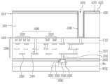
参考图9A和图10A,制造根据本发明构思的实施例的半导体器件的方法可以包括在衬底101的正面103上形成单元器件200(操作S102)。将参考图8A来理解对单元器件200的描述。单元器件200可以由第一层间绝缘层215覆盖。第一层间绝缘层215可以包括氧化硅。Referring to FIGS. 9A and 10A , a method of manufacturing a semiconductor device according to an embodiment of the inventive concept may include forming a
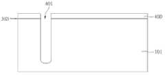
参考图9A和图10B,制造根据本发明构思的本实施例的半导体器件的方法可以包括在衬底101中形成TSV孔401(操作S104)。形成TSV孔401可以包括:在第一层间绝缘层215上形成TSV孔掩膜图案450,并且使用TSV孔掩膜图案450作为蚀刻掩膜对衬底101和第一层间绝缘层215进行蚀刻。TSV孔掩膜图案450可以包括氮化硅、氮氧化硅或有机材料。TSV孔401的最下端可以布置在衬底101的内部,例如,在主体中。TSV孔401可以不穿透衬底101的背面104。在形成TSV孔401后,可以除去TSV孔掩膜图案450。Referring to FIGS. 9A and 10B , the method of manufacturing the semiconductor device according to the present embodiment of the inventive concept may include forming the
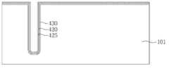
参考图9A和图10C,制造根据本发明构思的本实施例的半导体器件的方法可以包括在TSV孔401的内壁上共形地形成TSV衬垫430(操作S106)。TSV衬垫430可以包括氧化硅或氮化硅。例如,可以使用原子层沉积(ALD)工艺、等离子体增强化学气相沉积(PECVD)工艺或亚常压CVD(SACVD)工艺在TSV孔401的内壁上共形地沉积TSV衬垫430。可替换地,可以通过使用热氧化工艺来对TSV孔401的内壁进行热氧化而获得TSV衬垫430。在本实施例中,假设TSV衬垫430包括使用SACVD工艺形成的氧化硅层。Referring to FIGS. 9A and 10C , the method of manufacturing the semiconductor device according to the present embodiment of the inventive concept may include conformally forming the
参考图9A和图10D,制造根据本发明构思的本实施例的半导体器件的方法可以包括在TSV衬垫430上形成TSV阻挡层420和TSV种子层425(操作S108)。形成TSV阻挡层420可以包括使用诸如溅射工艺之类的物理气相沉积(PVD)工艺或金属有机CVD(MOCVD)工艺在TSV衬垫430上共形地形成阻挡金属。TSV阻挡层420可以包括Ti、TiN、Ta、TaN或WN。TSV阻挡层420可以形成为单层类型或多层类型。形成TSV种子层425可以包括使用PVD工艺或CVD工艺在TSV阻挡层420上共形地形成铜(Cu)、钌(Ru)、钨(W)或其它种子金属。Referring to FIGS. 9A and 10D , the method of manufacturing the semiconductor device according to the present embodiment of the inventive concept may include forming a
参考图9A和图10E,制造根据本发明构思的本实施例的半导体器件的方法可以包括形成TSV芯材料层410ml以填充TSV孔401(操作S110)。可以使用电镀工艺来形成TSV芯材料层410ml。当TSV种子层425和TSV芯材料层410ml包括相同的材料时,其间的边界可以消失。例如,当TSV种子层425和TSV芯材料层410ml包括铜(Cu)时,其间的边界可以消失。因此,在图10E中未示出TSV种子层425。Referring to FIGS. 9A and 10E , the method of manufacturing the semiconductor device according to the present embodiment of the inventive concept may include forming a TSV core material layer 410ml to fill the TSV hole 401 (operation S110 ). The TSV core material layer 410ml may be formed using an electroplating process. When the
参考图9A和图10F,制造根据本发明构思的本实施例的半导体器件的方法可以包括形成TSV结构400(操作S112)。TSV结构400可以包括TSV芯410、TSV阻挡层420和TSV衬垫430。形成TSV结构400可以包括使用CMP工艺来将可以在第一层间绝缘层215的顶部表面上形成的TSV芯材料层410ml、TSV种子层425和TSV衬垫430除去。例如,形成TSV结构400可以包括:使用第一CMP工艺来将TSV芯材料层410ml和TSV种子层425除去;使用第二CMP工艺来将TSV阻挡层420除去;以及使用湿法蚀刻工艺或清洗工艺来将TSV衬垫430除去。可替换地,形成TSV结构400可以包括:使用CMP工艺来将TSV芯材料层410ml和TSV种子层425除去;以及使用湿法蚀刻工艺或清洗工艺来将TSV阻挡层420和/或TSV衬垫430除去。Referring to FIGS. 9A and 10F , the method of manufacturing the semiconductor device according to the present embodiment of the inventive concept may include forming the TSV structure 400 (operation S112 ). The
参考图9A和图10G,制造根据本发明构思的本实施例的半导体器件的方法可以包括在衬底101的正面103上形成内部电路230(操作S114)。内部电路230可以包括多个导电的内部通孔240和多层的导电的内部互连250。每一个内部通孔240可以示出为垂直延伸的柱形,每一个内部互连250可以示出为水平延伸的台形。内部电路230可以由第一层间绝缘层215和第二层间绝缘层225覆盖。TSV焊盘260可以与衬底101的表面隔离开,并且形成在第二层间绝缘层225中。例如,TSV焊盘260可以形成在第一层间绝缘层215上。TSV焊盘260可以包括诸如W、Cu、Al之类的金属或其它金属。虽然第二层间绝缘层225将被形成为多层类型,但是为了简洁将第二层间绝缘层225示出为单层类型。Referring to FIGS. 9A and 10G , the method of manufacturing the semiconductor device according to the present embodiment of the inventive concept may include forming an
参考图9A和图10H,制造根据本发明构思的本实施例的半导体器件的方法可以包括在第二层间绝缘层225上形成正面I/O焊盘通孔插头270和正面钝化层265(操作S116)。正面I/O焊盘通孔插头270可以包括金属。例如,正面I/O焊盘通孔插头270可以包括最上面的金属层。正面钝化层265可以包括氮化硅、氧化硅或聚酰亚胺。正面钝化层265可以包括使正面I/O焊盘通孔插头270的上部暴露的下正面I/O焊盘开口311。Referring to FIGS. 9A and 10H , the method of manufacturing the semiconductor device according to the present embodiment of the inventive concept may include forming a front I/O pad via
参考图9A和图10I,制造根据本发明构思的本实施例的半导体器件的方法可以包括在下正面I/O焊盘开口311内形成正面I/O焊盘阻挡层320和正面I/O焊盘种子层330(操作S118)。形成正面I/O焊盘阻挡层320可以包括使用诸如溅射工艺之类的PVD工艺或MOCVD工艺在正面钝化层265上共形地形成阻挡金属。正面I/O焊盘阻挡层320可以包括Ti、TiN、Ta、TaN、WN或其它难熔金属。正面I/O焊盘阻挡层320可以形成为单层类型或多层类型。形成正面I/O焊盘种子层330可以包括使用诸如溅射工艺之类的PVD工艺或CVD工艺在正面I/O焊盘阻挡层320上共形地形成铜(Cu)、钌(Ru)、钨(W)或其它金属。Referring to FIGS. 9A and 10I , the method of manufacturing the semiconductor device according to the present embodiment of the inventive concept may include forming a front I/O
参考图9A和图10J,制造根据本发明构思的本实施例的半导体器件的方法可以包括在正面I/O焊盘种子层330上形成正面I/O焊盘掩膜图案340(操作S120)。正面I/O焊盘掩膜图案340可以具有使下正面I/O焊盘开口311暴露的上正面I/O焊盘开口312。正面I/O焊盘掩膜图案340可以包括光致抗蚀剂。Referring to FIGS. 9A and 10J , the method of manufacturing the semiconductor device according to the present embodiment of the inventive concept may include forming a front I/O
参考图9A和图10K,制造根据本发明构思的本实施例的半导体器件的方法可以包括形成初步的正面I/O焊盘300p(操作S122)。形成初步的正面I/O焊盘300p可以包括分别在下正面I/O焊盘开口311和上正面I/O焊盘开口312内形成正面I/O焊盘金属层350和正面I/O焊盘覆盖层360。形成正面I/O焊盘金属层350可以包括使用电镀工艺来形成诸如镍(Ni)或钨(W)之类的金属层。形成正面I/O焊盘覆盖层360可以包括在正面I/O焊盘金属层350上电镀金、镍或银。Referring to FIGS. 9A and 10K , the method of manufacturing the semiconductor device according to the present embodiment of the inventive concept may include forming a preliminary front I/
参考图9A和图10L,制造根据本发明构思的本实施例的半导体器件的方法可以包括形成正面I/O焊盘300(操作S124)。形成正面I/O焊盘300可以包括使用湿法蚀刻工艺来除去正面I/O焊盘掩膜图案340以及除去暴露在正面钝化层265上的正面I/O焊盘阻挡层320和正面I/O焊盘种子层330。Referring to FIGS. 9A and 10L , the method of manufacturing the semiconductor device according to the present embodiment of the inventive concept may include forming the front I/O pad 300 (operation S124 ). Forming the front I/
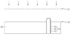
参考图9A和图10M,制造根据本发明构思的本实施例的半导体器件的方法可以包括将衬底101颠倒过来并且将衬底101安装在晶圆支撑载体WSC上(操作S126)。可以在晶圆支撑载体WSC上布置垫层Wc以保护正面I/O焊盘300不受物理冲击。Referring to FIGS. 9A and 10M , the method of manufacturing the semiconductor device according to the present embodiment of the inventive concept may include turning the
参考图9A和图10N,制造根据本发明构思的本实施例的半导体器件的方法可以包括地毯式地和/或选择性地将衬底101的背面104除去以使TSV结构400的背面端BE暴露(操作S128)。例如,可以使TSV结构400的背面端BE的顶部表面和部分侧表面暴露。将衬底101的背面104除去可以包括例如研磨工艺和/或回蚀工艺(etchbackprocess)。Referring to FIGS. 9A and 10N , the method of manufacturing a semiconductor device according to the present embodiment of the inventive concept may include blanket and/or selectively removing the
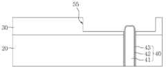
参考图9B和图10O,制造根据本发明构思的本实施例的半导体器件的方法可以包括形成背面绝缘层285以覆盖暴露的TSV结构400(操作S130)。背面绝缘层285可以是包括氮化硅的单层。Referring to FIGS. 9B and 10O , the method of manufacturing the semiconductor device according to the present embodiment of the inventive concept may include forming a
参考图9B和图10P,制造根据本发明构思的本实施例的半导体器件的方法可以包括在背面绝缘层285中形成槽550(操作S132)。槽550可以包括再分布槽551和对准标记槽552。再分布槽551可以使TSV结构400的一部分暴露。例如,再分布槽551可以使TSV结构400的背面端BE的顶部表面和侧表面暴露。在此工艺期间,可以将暴露的TSV衬垫430除去以使TSV阻挡层420暴露。Referring to FIGS. 9B and 10P , the method of manufacturing the semiconductor device according to the present embodiment of the inventive concept may include forming the
参考图9B和图10Q,制造根据本发明构思的本实施例的半导体器件的方法可以包括在再分布槽551内形成再分布阻挡层520和再分布种子层530(操作S134)。再分布阻挡层520和再分布种子层530可以共形地形成在再分布槽551的底部表面和内壁以及TSV结构400的暴露表面上。形成再分布阻挡层520可以包括使用诸如溅射工艺之类的PVD工艺或MOCVD工艺在背面绝缘层285上形成阻挡金属。再分布阻挡层520可以包括Ti、TiN、Ta、TaN、WN或其它难熔金属。再分布阻挡层520可以形成为单层类型或多层类型。形成再分布种子层530可以包括使用诸如溅射工艺之类的PVD工艺或CVD工艺在再分布阻挡层520上共形地形成铜(Cu)、钌(Ru)、钨(W)或其它金属。在此工艺期间,也可以在对准标记槽552内形成再分布阻挡层520和再分布种子层530。可以在TSV结构400的暴露表面上形成双层,例如TSV阻挡层420和再分布阻挡层520。Referring to FIGS. 9B and 10Q , the method of manufacturing the semiconductor device according to the present embodiment of the inventive concept may include forming a
参考图9B和图10R,制造根据本发明构思的本实施例的半导体器件的方法可以包括形成再分布互连材料层510a(操作S136)。形成再分布互连材料层510a可以包括使用电镀工艺来完全填充再分布槽551。当再分布互连材料层510a和再分布种子层530包括相同的材料时,其间的边界可以消失。为了附图的简介,再分布互连材料层510a和再分布种子层530之间的边界被省略。当再分布互连材料层510a和再分布种子层530包括不同的材料时,其间的边界可以存在。再分布互连材料层510a还可以填充对准标记槽552。Referring to FIGS. 9B and 10R , the method of manufacturing the semiconductor device according to the present embodiment of the inventive concept may include forming a redistribution
参考图9B和图10S,制造根据本发明构思的本实施例的半导体器件的方法可以包括形成再分布结构500(操作S138)。形成再分布结构500可以包括:使用CMP工艺来将暴露在背面绝缘层285的顶部表面上的再分布互连材料层510a、再分布种子层530和再分布阻挡层520除去。例如,形成再分布结构500可以包括:使用第一CMP工艺来将再分布互连材料层510a和再分布种子层530除去;以及使用第二CMP工艺来将再分布阻挡层520除去。在此工艺期间,可以形成再分布互连510和对准标记结构560。可替换地,形成再分布结构500可以包括:使用CMP工艺来将再分布互连材料层510a和再分布种子层530除去;以及使用湿法蚀刻工艺来将再分布阻挡层520除去。Referring to FIGS. 9B and 10S , the method of manufacturing the semiconductor device according to the present embodiment of the inventive concept may include forming a redistribution structure 500 (operation S138 ). Forming the
参考图9B和图10T,制造根据本发明构思的本实施例的半导体器件的方法可以包括形成背面钝化层275(操作S140)。背面钝化层275可以具有使再分布互连510的表面部分暴露的下背面I/O焊盘开口611。背面钝化层275可以包括氧化硅、氮化硅或聚酰亚胺。Referring to FIGS. 9B and 10T , the method of manufacturing the semiconductor device according to the present embodiment of the inventive concept may include forming a rear passivation layer 275 (operation S140 ).
参考图9B和图10U,制造根据本发明构思的本实施例的半导体器件的方法可以包括在下背面I/O焊盘开口611内和/或在背面钝化层275上形成背面I/O焊盘阻挡层620和背面I/O焊盘种子层630(操作S142)。形成背面I/O焊盘阻挡层620可以包括使用诸如溅射工艺之类的PVD工艺或MOCVD工艺在背面钝化层275上共形地形成阻挡金属。背面I/O焊盘阻挡层620可以包括Ti、TiN、Ta、TaN或WN。背面I/O焊盘阻挡层620可以形成为单层类型或多层类型。形成背面I/O焊盘种子层630可以包括使用诸如溅射工艺之类的PVD工艺或CVD工艺在背面I/O焊盘阻挡层620上形成铜(Cu)、钌(Ru)、钨(W)或其它金属。Referring to FIG. 9B and FIG. 10U, the method of manufacturing the semiconductor device according to the present embodiment of the present inventive concept may include forming a backside I/O pad within the lower backside I/
参考图9B和图10V,制造根据本发明构思的本实施例的半导体器件的方法可以包括在背面I/O焊盘阻挡层620和背面I/O焊盘种子层630上形成背面I/O焊盘掩膜图案640(操作S144)。背面I/O焊盘掩膜图案640可以具有使下背面I/O焊盘开口611暴露的上背面I/O焊盘开口612。背面I/O焊盘掩膜图案640可以包括光致抗蚀剂。Referring to FIG. 9B and FIG. 10V, the method of manufacturing the semiconductor device according to the present embodiment of the present inventive concept may include forming a backside I/O pad on the backside I/O
参考图9B和图10W,制造根据本发明构思的本实施例的半导体器件的方法可以包括形成初步的背面I/O焊盘600p(操作S146)。形成初步的背面I/O焊盘600p可以包括:在下背面I/O焊盘开口611和上背面I/O焊盘开口612内形成背面I/O焊盘金属层650和背面I/O焊盘覆盖层660。形成背面I/O焊盘金属层650可以包括使用电镀工艺来形成诸如镍(Ni)或钨(W)之类的金属层。形成背面I/O焊盘覆盖层660可以包括在背面I/O焊盘金属层650上电镀金(Au)或银(Ag)。Referring to FIGS. 9B and 10W , the method of manufacturing the semiconductor device according to the present embodiment of the inventive concept may include forming a preliminary rear I/
参考图9B和图10X,制造根据本发明构思的本实施例的半导体器件的方法可以包括形成背面I/O焊盘600(操作S148)。形成背面I/O焊盘600可以包括使用湿法蚀刻工艺来将背面I/O焊盘掩膜图案640除去并且将暴露在背面钝化层275上的背面I/O焊盘阻挡层620和背面I/O焊盘种子层630除去。随后,可以将所得到的结构从晶圆支撑载体WSC分离,从而完成图8A所示的半导体器件100A的形成。Referring to FIGS. 9B and 10X , the method of manufacturing the semiconductor device according to the present embodiment of the inventive concept may include forming the rear I/O pad 600 (operation S148 ). Forming the backside I/
图11A至图11D是示出了制造根据本发明构思的另一个实施例的半导体器件的方法的纵截面图。11A to 11D are longitudinal sectional views illustrating a method of manufacturing a semiconductor device according to another embodiment of the inventive concept.
参考图9C和图11A,制造根据本发明构思的本实施例的半导体器件的方法可以包括:参考图9A和图10A至图10N使TSV结构400的背面端BE暴露;以及形成下背面绝缘层287以覆盖TSV结构400的暴露的背面端BE(操作S129A)。下背面绝缘层287可以共形地形成在衬底101的表面和TSV结构400的暴露的表面上。下背面绝缘层287可以包括氧化硅。Referring to FIGS. 9C and 11A , the method of manufacturing the semiconductor device according to the present embodiment of the inventive concept may include: exposing the back end BE of the
参考图9C和图11B,制造根据本发明构思的本实施例的半导体器件的方法可以包括在下背面绝缘层287上形成上背面绝缘层289(操作S129B)。与下背面绝缘层287相比,上背面绝缘层289可以形成为更大的厚度。上背面绝缘层289可以包括氮化硅。Referring to FIGS. 9C and 11B , the method of manufacturing the semiconductor device according to the present embodiment of the inventive concept may include forming an upper
参考图9C和图11C,制造根据本发明构思的本实施例的半导体器件的方法可以包括在上背面绝缘层289中形成槽550以使TSV结构400的表面暴露(操作S132A)。槽550可以包括再分布槽551和对准标记槽552。再分布槽551可以使TSV结构400的背面端BE的顶部表面和侧表面暴露。在此工艺期间,可以将暴露的TSV衬垫430除去。下背面绝缘层287的一部分可以暴露在再分布槽551的底部表面上。Referring to FIGS. 9C and 11C , the method of manufacturing the semiconductor device according to the present embodiment of the inventive concept may include forming a
参考图9C和图11D,制造根据本发明构思的本实施例的半导体器件的方法可以包括通过执行参考图9B和图10Q至图10X所描述的各工艺(操作S134至S148)来形成背面I/O焊盘600。再分布阻挡层520的一部分和下背面绝缘层287的一部分可以与TSV结构400的侧表面接触。Referring to FIGS. 9C and 11D , the method of manufacturing the semiconductor device according to the present embodiment of the inventive concept may include forming the backside I/
图12A至图12G是示出了制造根据本发明构思的另一个实施例的半导体器件的方法的纵截面图。12A to 12G are longitudinal sectional views illustrating a method of manufacturing a semiconductor device according to another embodiment of the inventive concept.
参考图9D和图12A,制造根据本发明构思的本实施例的半导体器件的方法可以包括在衬底101中形成TSV孔401(操作S202)。在衬底101中形成TSV孔401可以包括在衬底101的正面103上形成TSV孔掩膜图案450,并且使用TSV孔掩膜图案450作为蚀刻掩膜对衬底101进行蚀刻。TSV孔掩膜图案450可以包括氧化硅和/或氮化硅。TSV孔掩膜图案450可以形成为单层类型或多层类型。例如,可以在衬底101上形成氧化硅层,并且可以在氧化硅层上形成氮化硅层。在本实施例中,在概念上假设TSV孔掩膜图案450为单材料层。TSV孔401的最下端可以布置在衬底101中,例如,在主体中。在形成TSV孔401后,可以除去TSV孔掩膜图案450。Referring to FIGS. 9D and 12A , the method of manufacturing the semiconductor device according to the present embodiment of the inventive concept may include forming the
参考图9D和图12B,制造根据本发明构思的本实施例的半导体器件的方法可以包括在TSV孔401的内壁上共形地形成TSV衬垫430(操作S204)。然后,制造根据本发明构思的本实施例的半导体器件的方法可以包括在TSV衬垫430上共形地形成TSV阻挡层420和TSV种子层425(操作S206)。Referring to FIGS. 9D and 12B , the method of manufacturing the semiconductor device according to the present embodiment of the inventive concept may include conformally forming the
参考图9D和图12C,制造根据本发明构思的本实施例的半导体器件的方法可以包括形成TSV芯材料层410ml以填充TSV孔401(操作S208)。Referring to FIGS. 9D and 12C , the method of manufacturing the semiconductor device according to the present embodiment of the inventive concept may include forming a TSV core material layer 410ml to fill the TSV hole 401 (operation S208 ).
参考图9D和图12D,制造根据本发明构思的本实施例的半导体器件的方法可以包括形成TSV结构400(操作S210)。Referring to FIGS. 9D and 12D , the method of manufacturing the semiconductor device according to the present embodiment of the inventive concept may include forming the TSV structure 400 (operation S210 ).
参考图9D和图12E,制造根据本发明构思的本实施例的半导体器件的方法可以包括形成内部电路230和正面I/O焊盘300(操作S212)。可以不形成图10G至图11D的TSV焊盘260。例如,TSV结构400可以与内部通孔240中的一个直接接触。Referring to FIGS. 9D and 12E , the method of manufacturing the semiconductor device according to the present embodiment of the inventive concept may include forming the
参考图9D和图12F,制造根据本发明构思的本实施例的半导体器件的方法可以包括将衬底101颠倒过来并且将衬底101安装在晶圆支撑载体WSC上(操作S214)。而且,该方法可以包括地毯式地和/或选择性地除去衬底101的背面104以使TSV结构400的一部分暴露(操作S216)。Referring to FIGS. 9D and 12F , the method of manufacturing the semiconductor device according to the present embodiment of the inventive concept may include turning the
参考图9E和图12G并且还参考图10O至图10X,制造根据本发明构思的本实施例的半导体器件的方法可以包括:形成背面绝缘层285以覆盖暴露的TSV结构400(操作S218);在背面绝缘层285中形成槽550(操作S220);在槽550中形成再分布阻挡层520和再分布种子层530(操作S222);形成再分布互连材料层510a(操作S224);形成再分布结构500(操作S226);形成具有下背面I/O焊盘开口611以使再分布互连510的表面部分暴露的背面钝化层275(操作S228);在下背面I/O焊盘开口611内和/或在背面钝化层275上,形成背面I/O焊盘阻挡层620和背面I/O焊盘种子层630(操作S230);在背面I/O焊盘阻挡层620和背面I/O焊盘种子层630上,形成具有上背面I/O焊盘开口612以使下背面I/O焊盘开口611暴露的背面I/O焊盘掩膜图案640(操作S232);形成初步的背面I/O焊盘600p(操作S234);以及形成背面I/O焊盘600(操作S236)。示例性地示出了再分布种子层530和再分布互连510之间的边界。Referring to FIGS. 9E and 12G and also referring to FIGS. 10O to 10X , the method of manufacturing the semiconductor device according to the present embodiment of the inventive concept may include: forming a backside insulating layer 285 to cover the exposed TSV structure 400 (operation S218 ); forming a groove 550 in the back insulating layer 285 (operation S220); forming a redistribution barrier layer 520 and a redistribution seed layer 530 in the groove 550 (operation S222); forming a redistribution interconnect material layer 510a (operation S224); forming a redistribution structure 500 (operation S226); forming a backside passivation layer 275 having a lower backside I/O pad opening 611 to partially expose the surface of the redistribution interconnect 510 (operation S228); within the lower backside I/O pad opening 611 And/or on the back passivation layer 275, form a back I/O pad barrier layer 620 and a back I/O pad seed layer 630 (operation S230); on the back I/O pad barrier layer 620 and the back I/O On the O pad seed layer 630, a back I/O pad mask pattern 640 having an upper back I/O pad opening 612 to expose the lower back I/O pad opening 611 is formed (operation S232); forming a preliminary the rear I/O pads 600p (operation S234); and forming the rear I/O pads 600 (operation S236). The boundary between the
图13A至图13D是示出了制造根据本发明构思的另一个实施例的半导体器件的方法的纵截面图。13A to 13D are longitudinal sectional views illustrating a method of manufacturing a semiconductor device according to another embodiment of the inventive concept.
参考图9F和图13A,制造根据本发明构思的本实施例的半导体器件的方法可以包括参考图9D和图12A至图12F使TSV结构400的背面端BE暴露,并且形成下背面绝缘层287以覆盖在衬底101的背面104上暴露的TSV结构400(操作S219A)。Referring to FIGS. 9F and 13A , the method of manufacturing the semiconductor device according to the present embodiment of the inventive concept may include exposing the backside end BE of the
参考图9F和图13B,制造根据本发明构思的本实施例的半导体器件的方法可以包括在下背面绝缘层287上形成上背面绝缘层289(操作S219B)。Referring to FIGS. 9F and 13B , the method of manufacturing the semiconductor device according to the present embodiment of the inventive concept may include forming an upper
参考图9F和图13C,制造根据本发明构思的本实施例的半导体器件的方法可以包括在上背面绝缘层289中形成再分布槽551以使TSV结构400的表面暴露(操作S220A)。例如,再分布槽551可以使TSV结构400的背面端BE的顶部表面和侧表面暴露。在此工艺期间,可以除去暴露的TSV衬垫430。下背面绝缘层287的一部分可以暴露在再分布槽551的底部表面上。Referring to FIGS. 9F and 13C , the method of manufacturing the semiconductor device according to the present embodiment of the inventive concepts may include forming
参考图9E和图13D,制造根据本发明构思的本实施例的半导体器件的方法可以包括:在槽550内形成再分布阻挡层520和再分布种子层530(操作S222);形成再分布互连材料层510a(操作S224);形成再分布结构500(操作S226);形成具有下背面I/O焊盘开口611以使再分布互连510的表面部分暴露的背面钝化层275(操作S228);在下背面I/O焊盘开口611内和/或在背面钝化层275上,形成背面I/O焊盘阻挡层620和背面I/O焊盘种子层630(操作S230);在背面I/O焊盘阻挡层620和背面I/O焊盘种子层630上,形成具有上背面I/O焊盘开口612以使下背面I/O焊盘开口611暴露的背面I/O焊盘掩膜图案640(操作S232);形成初步的背面I/O焊盘600p(操作S234);以及形成背面I/O焊盘600(操作S236)。Referring to FIG. 9E and FIG. 13D , the method of manufacturing the semiconductor device according to the present embodiment of the inventive concept may include: forming a
图14A至图14Q是在制造根据本发明构思的各个实施例的半导体器件的方法中,具有各种形状的TSV结构400a至400q的概念纵截面图,TSV结构400a至400q暴露在再分布槽551内。14A to 14Q are conceptual longitudinal cross-sectional views of
参考图14A,可以从突出至再分布槽551内的TSV结构400a的背面端BEa除去TSV衬垫430a,以使TSV阻挡层420a暴露。TSV阻挡层420a可以覆盖TSV芯410a的整个表面。Referring to FIG. 14A, the
参考图14B,在突出至再分布槽551内的TSV结构400b的背面端BEb中,TSV衬垫430b可以使TSV阻挡层420b的顶端的表面暴露并且部分或全部覆盖TSV阻挡层420b的侧表面。TSV阻挡层420b可以覆盖TSV芯410b的整个表面。Referring to FIG. 14B , in the backside end BEb of the TSV structure 400b protruding into the
参考图14C,在突出至再分布槽551内的TSV结构400c的背面端BEc中,TSV阻挡层420c可以使TSV芯410c的顶端的表面暴露并且部分或全部覆盖TSV芯410c的侧表面,TSV衬垫430c可以使突出至再分布槽551内的TSV阻挡层420c的顶端的表面暴露并且覆盖TSV阻挡层420c的整个侧表面。Referring to FIG. 14C, in the back end BEc of the
参考图14D,在突出至再分布槽551内的TSV结构400d的背面端BEd中,TSV阻挡层420d可以使TSV芯410d的顶端的表面暴露并且部分或全部覆盖TSV芯410d的侧表面,TSV衬垫430d可以使突出至再分布槽551内的TSV阻挡层420d的顶端的表面暴露并且部分覆盖TSV阻挡层420d的侧表面。Referring to FIG. 14D, in the back end BEd of the
参考图14E,在突出至再分布槽551内的TSV结构400e的背面端BEe中,TSV阻挡层420e可以使TSV芯410e的顶端的表面暴露并且部分或全部覆盖TSV芯410e的侧表面,TSV衬垫430e可以使突出至再分布槽551内的TSV阻挡层420e的顶端和侧表面暴露。例如,TSV衬垫430e的顶端可以形成在与再分布槽551的底部表面相同的水平或相似的水平处。Referring to FIG. 14E, in the backside end BEe of the
参考图14F,在突出至再分布槽551内的TSV结构400f的背面端BEf中,可以将TSV阻挡层420f和TSV衬垫430f除去以使TSV芯410f的顶端和侧表面全部暴露。Referring to FIG. 14F , in the backside end BEf of the
参考图14G,在突出至再分布槽551内的TSV结构400g的背面端BEg中,下背面绝缘层287的顶端的一部分可以暴露在上背面绝缘层289的再分布槽551内。TSV芯410g和TSV阻挡层420g可以突出至再分布槽551内。下背面绝缘层287可以包围TSV结构400g,并且与TSV衬垫430g的侧表面接触。上背面绝缘层289可以与TSV衬垫430g隔离开,并且不与TSV衬垫430g接触。TSV阻挡层420g可以覆盖突出的TSV芯410g的顶部表面和侧表面。在再分布槽551内,TSV衬垫430g的顶部表面、下背面绝缘层287的顶部表面和上背面绝缘层289的顶部表面可以布置在相同的水平或相似的水平处。Referring to FIG. 14G , in the backside end BEg of the
参考图14H,在突出至再分布槽551内的TSV结构400h的背面端BEh中,TSV衬垫430h的顶端可以突出至再分布槽551内。Referring to FIG. 14H , in the backside end BEh of the
参考图14I,在突出至再分布槽551内的TSV结构400i的背面端BEi中,TSV衬垫430i的顶端和下背面绝缘层287的顶端可以突出至再分布槽551内。TSV衬垫430i的顶端和下背面绝缘层287的顶端可以布置在相同的水平或相似的水平处。Referring to FIG. 14I , in the backside end BEi of the
参考图14J,在突出至再分布槽551内的TSV结构400j的背面端BEj中,TSV衬垫430j的顶端和下背面绝缘层287的顶端可以突出至再分布槽551内,并且TSV衬垫430j的顶端可以布置在比下背面绝缘层287的顶端高的水平处。14J, in the backside end BEj of the
参考图14K,在突出至再分布槽551内的TSV结构400k的背面端BEk中,TSV芯410k可以突出至再分布槽551内,并且TSV阻挡层420k可以部分覆盖TSV芯410k的侧表面。TSV阻挡层420k的顶端、TSV衬垫430k的顶端、下背面绝缘层287的顶端和上背面绝缘层289的顶端可以布置在相同的水平或相似的水平处。14K, in the back side BEk of the
参考图14L,在突出至再分布槽551内的TSV结构400l的背面端BEl中,TSV芯410l可以突出至再分布槽551内,并且TSV阻挡层420l可以部分或全部覆盖TSV芯410l的侧表面。TSV阻挡层420l可以突出至再分布槽551内。TSV衬垫430l的顶端、下背面绝缘层287的顶端和上背面绝缘层289的顶端可以布置在相同的水平或相似的水平处。Referring to FIG. 14L, in the back end BE1 of the TSV structure 400l protruding into the
参考图14M,在突出至再分布槽551内的TSV结构400m的背面端BEm中,TSV芯410m可以突出至再分布槽551内,TSV阻挡层420m可以突出至再分布槽551内并且部分或全部覆盖TSV芯410m的侧表面。TSV衬垫430m可以突出至再分布槽551内并且部分或全部覆盖TSV阻挡层420m的侧表面。Referring to FIG. 14M, in the back end BEm of the
参考图14N,在突出至再分布槽551内的TSV结构400n的背面端BEn中,TSV芯410n可以突出至再分布槽551内,TSV阻挡层420n可以突出至再分布槽551内并且部分或全部覆盖TSV芯410n的侧表面。TSV衬垫430n可以突出至再分布槽551内并且全部覆盖TSV阻挡层420n的侧表面。下背面绝缘层287的一部分可以突出至再分布槽551内,并且全部覆盖TSV衬垫430n的侧表面。Referring to FIG. 14N, in the backside end BEn of the
参考图14O,在突出至再分布槽551内的TSV结构400o的背面端BEo中,TSV芯410o可以突出至再分布槽551内,TSV阻挡层420o可以突出至再分布槽551内并且部分或全部覆盖TSV芯410o的侧表面。TSV衬垫430o可以突出至再分布槽551内并且部分或全部覆盖TSV阻挡层420o的侧表面。下背面绝缘层287的顶部表面可布置在与上背面绝缘层289的表面相同的水平或相似的水平处。Referring to FIG. 14O, in the back side BEo of the TSV structure 400o protruding into the
参考图14P,在突出至再分布槽551内的TSV结构400p的背面端BEp中,TSV芯410p可以突出至再分布槽551内,TSV阻挡层420p可以突出至再分布槽551内并且部分或全部覆盖TSV芯410p的侧表面。TSV衬垫430p可以突出至再分布槽551内并且部分或全部覆盖TSV阻挡层420p的侧表面。下背面绝缘层287的一部分可以突出至再分布槽551内,并且部分或全部覆盖TSV衬垫430p的侧表面。Referring to FIG. 14P, in the back end BEp of the
参考图14Q,在突出至再分布槽551内的TSV结构400q的背面端BEq中,TSV芯410q可以突出至再分布槽551内,TSV阻挡层420q可以突出至再分布槽551内并且部分或全部覆盖TSV芯410q的侧表面。TSV衬垫430q可以突出至再分布槽551内并且全部覆盖TSV阻挡层420q的侧表面。TSV阻挡层420q的顶端和TSV衬垫430q的顶端可以布置在相同的水平或相似的水平处。下背面绝缘层287的一部分可以突出至再分布槽551内,并且部分或全部覆盖TSV衬垫430q的侧表面。Referring to FIG. 14Q, in the back end BEq of the TSV structure 400q protruding into the
图15A至图15M是示出了制造根据本发明构思的另一个实施例的半导体器件的方法的纵截面图。15A to 15M are longitudinal sectional views illustrating a method of manufacturing a semiconductor device according to another embodiment of the inventive concept.
参考图9G和图15A,制造根据本发明构思的实施例的半导体器件的方法可以包括在衬底101上形成内部电路230和正面I/O焊盘300(操作S302)。在此工艺期间,可以形成TSV焊盘260。Referring to FIGS. 9G and 15A , a method of manufacturing a semiconductor device according to an embodiment of the inventive concept may include forming an
参考图9G和图15B,制造根据本发明构思的本实施例的半导体器件的方法可以包括将衬底101颠倒过来并且将衬底101安装在晶圆支撑载体WSC上(操作S304)。Referring to FIGS. 9G and 15B , the method of manufacturing the semiconductor device according to the present embodiment of the inventive concept may include turning the
参考图9G和图15C,制造根据本发明构思的本实施例的半导体器件的方法可以包括在衬底101中形成TSV孔401(操作S306)。形成TSV孔401可以包括在衬底101的背面104上形成TSV孔掩膜图案450,并且使用TSV孔掩膜图案450作为蚀刻掩膜对衬底101进行蚀刻。TSV孔掩膜图案450可以包括氧化硅或氮化硅。TSV孔掩膜图案450可以形成为单层类型或多层类型。例如,可以在衬底101上形成氧化硅层,并且在氧化硅层上形成氮化硅层。在本实施例中,在概念上假设TSV孔掩膜图案450为单材料层。然后,可以除去TSV孔掩膜图案450。本实施例描述了未除去而是保留TSV孔掩膜图案450的示例性情况。在形成TSV孔401前,可以执行将衬底101的背面104地毯式地除去以使衬底101变薄的工艺。Referring to FIGS. 9G and 15C , the method of manufacturing the semiconductor device according to the present embodiment of the inventive concept may include forming the
参考图9G和图15D,制造根据本发明构思的本实施例的半导体器件的方法可以包括在TSV孔401的内壁和底部上共形地形成TSV衬垫430(操作S308)。Referring to FIGS. 9G and 15D , the method of manufacturing the semiconductor device according to the present embodiment of the inventive concept may include conformally forming the
参考图9G和图15E,制造根据本发明构思的本实施例的半导体器件的方法可以包括将在TSV孔401的底部形成的TSV衬垫430除去(操作S310)。在此工艺期间,可以将TSV孔掩膜图案450变薄或除去。本实施例描述了将TSV孔掩膜图案450变薄的示例性情况。Referring to FIGS. 9G and 15E , the method of manufacturing the semiconductor device according to the present embodiment of the inventive concept may include removing the
参考图9G和图15F,制造根据本发明构思的本实施例的半导体器件的方法可以包括在TSV衬垫430上共形地形成TSV阻挡层420和TSV种子层425(操作S312)。Referring to FIGS. 9G and 15F , the method of manufacturing the semiconductor device according to the present embodiment of the inventive concept may include conformally forming the
参考图9G和图15G,制造根据本发明构思的本实施例的半导体器件的方法可以包括形成TSV芯材料层410ml以填充TSV孔401(操作S314)。Referring to FIGS. 9G and 15G , the method of manufacturing the semiconductor device according to the present embodiment of the inventive concept may include forming a TSV core material layer 410ml to fill the TSV hole 401 (operation S314 ).
参考图9G和图15H,制造根据本发明构思的本实施例的半导体器件的方法可以包括形成TSV结构400(操作S316)。形成TSV结构400可以包括使用CMP工艺和/或回蚀工艺来将在衬底101的背面104上形成的TSV芯材料层410ml、TSV种子层425、TSV阻挡层420、TSV衬垫430和/或TSV孔掩膜图案450除去。Referring to FIGS. 9G and 15H , the method of manufacturing the semiconductor device according to the present embodiment of the inventive concept may include forming the TSV structure 400 (operation S316 ). Forming the
参考图9G和图15I,制造根据本发明构思的该实施例的半导体器件的方法可以包括将衬底101的背面104地毯式地和/或选择性地除去以使TSV结构400的一部分暴露(操作S318)。TSV阻挡层420可以暴露在TSV结构400的顶部表面上。Referring to FIGS. 9G and 15I , the method of manufacturing the semiconductor device according to this embodiment of the inventive concept may include blanket and/or selectively removing the
参考图9G和图15J,制造根据本发明构思的本实施例的半导体器件的方法可以包括形成背面绝缘层285以覆盖暴露的TSV结构400(操作S320)。例如,可以在衬底101和背面绝缘层285之间插入氧化硅。Referring to FIGS. 9G and 15J , the method of manufacturing the semiconductor device according to the present embodiment of the inventive concept may include forming a
参考图9G和图15K,制造根据本发明构思的本实施例的半导体器件的方法可以包括在背面绝缘层285中形成槽550(操作S322)。在此工艺期间,可以除去暴露的TSV衬垫430。Referring to FIGS. 9G and 15K , the method of manufacturing the semiconductor device according to the present embodiment of the inventive concept may include forming the
参考图9G和图15L,制造根据本发明构思的本实施例的半导体器件的方法可以包括在再分布槽551内形成再分布阻挡层520和再分布种子层530(操作S324)。再分布阻挡层520和再分布种子层530可以共形地形成在再分布槽551的底部表面和内壁以及暴露的TSV结构400上。Referring to FIGS. 9G and 15L , the method of manufacturing the semiconductor device according to the present embodiment of the inventive concept may include forming a
参考图9H和图15M,制造根据本发明构思的本实施例的半导体器件的方法可以包括:通过执行参考图10R至图10X来描述的各工艺来形成再分布互连材料层510a(操作S326);形成再分布结构500(操作S328);形成具有下背面I/O焊盘开口611以使再分布互连510的表面部分暴露的背面钝化层275(操作S330);在下背面I/O焊盘开口611内和/或在背面钝化层275上,形成背面I/O焊盘阻挡层620和背面I/O焊盘种子层630(操作S332);在背面I/O焊盘阻挡层620和背面I/O焊盘种子层630上,形成背面I/O焊盘掩膜图案640(操作S334);形成初步的背面I/O焊盘600p(操作S336);以及形成背面I/O焊盘600(操作S338)。Referring to FIGS. 9H and 15M , the method of manufacturing the semiconductor device according to the present embodiment of the inventive concept may include forming a redistribution
图16A至图16K是示出了制造根据本发明构思的另一个实施例的半导体器件的方法的纵截面图。16A to 16K are longitudinal sectional views illustrating a method of manufacturing a semiconductor device according to another embodiment of the inventive concept.
参考图16A并且还参考图9G、图15A和图15B,制造根据本发明构思的该实施例的半导体器件的方法可以包括:在衬底101上形成内部电路230和正面I/O焊盘300(操作S302);将衬底101颠倒过来并且将衬底101安装在晶圆支撑载体WSC上(操作S304);以及在衬底101的背面104上形成TSV孔掩膜图案450(操作S306)。TSV孔掩膜图案450可以形成为多层类型。例如,TSV孔掩膜图案450可以包括包含氧化硅的下TSV孔掩膜图案451和包含氮化硅的上TSV孔掩膜图案452。Referring to FIG. 16A and also referring to FIGS. 9G, 15A, and 15B, the method of manufacturing a semiconductor device according to this embodiment of the inventive concept may include forming an
参考图9I和图16B,制造根据本发明构思的本实施例的半导体器件的方法可以包括形成TSV孔401(操作S408)。Referring to FIGS. 9I and 16B , the method of manufacturing the semiconductor device according to the present embodiment of the inventive concept may include forming the TSV hole 401 (operation S408 ).
参考图9I和图16C,制造根据本发明构思的本实施例的半导体器件的方法可以包括在TSV孔401的内壁上共形地形成TSV衬垫430(操作S410)。Referring to FIGS. 9I and 16C , the method of manufacturing the semiconductor device according to the present embodiment of the inventive concept may include conformally forming the
参考图9I和图16D,制造根据本发明构思的本实施例的半导体器件的方法可以包括将布置在TSV孔401的底部表面上的TSV衬垫430部分地除去(操作S412)。在此工艺期间,还可以将在TSV孔掩膜图案450上形成的TSV衬垫430除去。Referring to FIGS. 9I and 16D , the method of manufacturing the semiconductor device according to the present embodiment of the inventive concept may include partially removing the
参考图9I和图16E,制造根据本发明构思的本实施例的半导体器件的方法可以包括在TSV衬垫430上共形地形成TSV阻挡层420和TSV种子层425(操作S414)。Referring to FIGS. 9I and 16E , the method of manufacturing the semiconductor device according to the present embodiment of the inventive concept may include conformally forming the
参考图9I和图16F,制造根据本发明构思的本实施例的半导体器件的方法可以包括形成TSV芯材料层410ml以填充TSV孔401(操作S416)。在图16F中,省略了TSV种子层425和TSV芯材料层410ml之间的边界。Referring to FIGS. 9I and 16F , the method of manufacturing the semiconductor device according to the present embodiment of the inventive concept may include forming a TSV core material layer 410ml to fill the TSV hole 401 (operation S416 ). In FIG. 16F, the boundary between the
参考图9I和图16G,制造根据本发明构思的本实施例的半导体器件的方法可以包括形成TSV结构400(操作S418)。形成TSV结构400可以包括使用CMP工艺和/或蚀刻工艺来将在上TSV孔掩膜图案452上形成的TSV芯材料层410ml和TSV阻挡层420除去。Referring to FIGS. 9I and 16G , the method of manufacturing the semiconductor device according to the present embodiment of the inventive concept may include forming the TSV structure 400 (operation S418 ). Forming the
参考图9I和图16H,制造根据本发明构思的本实施例的半导体器件的方法可以包括形成背面绝缘层285以覆盖暴露的TSV结构400(操作S420)。当背面绝缘层285和上TSV孔掩膜图案452包括相同的材料时,其间的边界可以消失。Referring to FIGS. 9I and 16H , the method of manufacturing the semiconductor device according to the present embodiment of the inventive concept may include forming a
参考图9I和图16I,制造根据本发明构思的本实施例的半导体器件的方法可以包括在背面绝缘层285中形成槽550(操作S422)。槽550可以包括再分布槽551和对准标记槽552。再分布槽551可以使TSV结构400的一端暴露。在此工艺期间,可以将在TSV结构400的暴露的表面上形成的TSV衬垫430除去。例如,TSV阻挡层420可以暴露在再分布槽551内。Referring to FIGS. 9I and 16I , the method of manufacturing the semiconductor device according to the present embodiment of the inventive concept may include forming the
参考图9I和图16J,制造根据本发明构思的该实施例的半导体器件的方法可以包括在背面绝缘层285上形成再分布阻挡层520和再分布种子层530(操作S424)。再分布阻挡层520和再分布种子层530可以共形地形成在再分布槽551的底部表面和内壁以及暴露的TSV结构400上。Referring to FIGS. 9I and 16J , the method of manufacturing the semiconductor device according to this embodiment of the inventive concept may include forming a
参考图9J和图16K,制造根据本发明构思的本实施例的半导体器件的方法可以包括:通过执行参考图9L和图10R至图10X来描述的各工艺来形成再分布互连材料层510a(操作S426);形成再分布结构500(操作S428);形成具有下背面I/O焊盘开口611以使再分布互连510的表面部分暴露的背面钝化层275(操作S430);在下背面I/O焊盘开口611内和/或在背面钝化层275上,形成背面I/O焊盘阻挡层620和背面I/O焊盘种子层630(操作S432);在背面I/O焊盘阻挡层620和背面I/O焊盘种子层630上,形成背面I/O焊盘掩膜图案640(操作S434);形成初步的背面I/O焊盘600p(操作S436);以及形成背面I/O焊盘600(操作S438)。没有示出再分布互连510和再分布种子层530之间的边界。例如,可以形成图8R所示的半导体器件100R。Referring to FIGS. 9J and 16K , the method of manufacturing the semiconductor device according to the present embodiment of the inventive concept may include forming a redistribution
制造根据本发明构思的各个实施例的各半导体器件的各方法可以包括使用大马士革工艺来形成再分布结构500。因此,再分布阻挡层520可以完全包围再分布互连510的底部表面和侧表面。例如,当使用湿法蚀刻工艺或选择性蚀刻工艺来除去再分布阻挡层520时,再分布阻挡层520可能不完全包围再分布互连510的底部或侧表面,因而引起物理的和/或电的不稳定。代替光刻和蚀刻工艺,制造根据本发明构思的各个实施例的各半导体器件的各方法可以采用CMP工艺。因此,TSV结构400的节距和再分布结构500的节距可以变得更微小和更复杂。在制造根据本发明构思的各个实施例的各半导体器件的各方法的每一个方法中,TSV结构400可以突出至再分布结构500中。例如,TSV结构400可以插入再分布结构500中。因此,TSV结构400与再分布结构500之间的接触面积可以增加,使得TSV结构400与再分布结构500之间的薄层电阻可以减小。而且,由于再分布结构500可以由TSV结构400进行物理固定,因此可以防止由浮动现象引起的各组件的接触故障或分离。在制造根据本发明构思的各个实施例的各半导体器件的各方法中,可以同时形成再分布结构500和对准标记结构560。形成对准标记结构560的附加工艺可以省略。再分布槽551和对准标记槽552可以同时形成至相同的深度。再分布阻挡层520和对准标记阻挡层570可以由相同的材料同时形成。再分布互连510和对准标记图案580可以由相同的材料同时形成。因此,可以简化用于形成半导体器件的工艺,以提高生产力和降低制造成本。Various methods of manufacturing semiconductor devices according to various embodiments of the inventive concept may include forming the
图17A至图17D是根据本发明构思的各个实施例的半导体器件的层叠结构1000A至1000D的概念纵截面图。17A to 17D are conceptual longitudinal cross-sectional views of
参考图17A,根据本发明构思的一个实施例的半导体器件的层叠结构1000A可以包括下半导体器件1100和上半导体器件1200。可以通过使用凸块1010来将下半导体器件1100的正面I/O焊盘1130和上半导体器件1200的背面I/O焊盘1260彼此电连接。例如,可以获得半导体器件层叠结构1000A,其中下半导体器件1100的正面I/O焊盘1130和上半导体器件1200的背面I/O焊盘1260可以电连接。凸块1010可以包括焊接材料。例如,凸块1010可以包括锡(Sn)、银(Ag)和铜(Cu)。凸块1010还可以包括镍(Ni)。下半导体器件1100和上半导体器件1200可以具有相同的结构。例如,正面I/O焊盘1130和背面I/O焊盘1260可以彼此垂直对准。Referring to FIG. 17A , a
参考图17B,根据本发明构思的另一个实施例的半导体器件的层叠结构1000B可以包括顺序层叠的多个半导体器件1100、1200、1300和1400。例如,层叠结构1000B可以包括相同结构的多个半导体器件1100、1200、1300和1400。正面I/O焊盘1130、1230、1330和1430以及背面I/O焊盘1160、1260、1360和1460可以相互垂直对准。半导体器件的层叠结构1000B可以包括例如与2的幂相等的数量的半导体器件,例如4、8、16或32。正面I/O焊盘1130、1230、1330和1430以及背面I/O焊盘1160、1260、1360和1460的相邻焊盘可以分别通过凸块1010、1020和1030相互物理和/或电气连接。例如,最下面的半导体器件1100的正面I/O焊盘1130可以电连接至最上面的半导体器件1400的背面I/O焊盘1460。Referring to FIG. 17B , a
参考图17C,根据本发明构思的另一个实施例的半导体器件的层叠结构1000C可以包括下半导体器件1100和上半导体器件1200。例如,下半导体器件1100可以包括逻辑器件,上半导体器件1200可以包括存储器件。例如,下半导体器件1100的正面I/O焊盘1130可以物理和/或电气连接至上半导体器件1200的背面I/O焊盘1260。Referring to FIG. 17C , a
参考图17D,根据本发明构思的另一个实施例的半导体器件的层叠结构1000D可以包括下半导体器件1500和多个上半导体器件1100、1200、1300和1400。例如,下半导体器件1500可以包括逻辑器件,上半导体器件1100、1200、1300和1400可以包括存储器件。通过使用凸块1010、1020、1030和1050,半导体器件1100、1200、1300、1400和1500的正面I/O焊盘1130、1230、1330和1530以及半导体器件1100、1200、1300和1400的背面I/O焊盘1160、1260、1360和1460可以相互电连接。Referring to FIG. 17D , a
图18是根据本发明构思的实施例的半导体封装件1600的概念纵截面图。参考图18,根据本发明构思的本实施例的半导体封装件1600可以包括层叠在封装件衬底1610上的多个半导体器件1100、1200、1300和1400。例如,半导体器件1100、1200、1300和1400中的每一个可以包括闪存器件。通过使用凸块1060,最下面的半导体器件1100的背面I/O焊盘1160可以电连接至封装件衬底1610的凸块连接盘(bumpland)1630。FIG. 18 is a conceptual longitudinal sectional view of a
图19是根据本发明构思的实施例的模块2200的概念图,模块2200包括根据本发明构思的实施例的半导体器件。参考图19,根据本发明构思的该实施例的模块2200可以包括安装在模块衬底2210上的半导体封装件2230。半导体封装件2230可以包括根据本发明构思的各个实施例的通孔连接结构10A至10S或半导体器件100A至100Q中的至少一个。模块2200还可以包括安装在模块衬底2210上的微处理器(MP)2220。输入/输出(I/O)端子2240可以布置在模块衬底2210的至少一侧上。FIG. 19 is a conceptual diagram of a
图20是包括根据本发明构思的各个实施例的通孔连接结构10A至10S或半导体器件100A至100Q中的至少一个的电子系统2300的概念框图。参考图20,根据本发明构思的各个实施例的通孔连接结构10A至10S或半导体器件100A至100Q可以应用于电子系统2300。电子系统2300可以包括主体2310、MP单元2320、电源2330、功能单元2340和/或显示控制单元2350。主体2310可以包括含有印刷电路板(PCB)的系统板或主板。MP单元2320、电源2330、功能单元2340和显示控制单元2350可以安装在主体2310上。可以在主体2310的顶部表面上或在主体2310的外部布置显示单元2360。例如,显示单元2360可以布置在主体2310的表面上,并且显示由显示控制单元2350处理的图像。电源2330可以从外部电池(未示出)接收预定的电压,将该电压分成具有所需的电压电平的各个电压,并且将各个分压提供给MP单元2320、功能单元2340和显示控制单元2350。MP单元2320可以接收来自电源2330的电压,并且控制功能单元2340和显示单元2360。功能单元2340可以提供电子系统2300的各种功能。例如,当电子系统2300是诸如便携式电话之类的移动电子产品时,功能单元2340可以包括若干组件,这些组件能够提供无线通信功能,例如,通过拨号外部设备2370或与外部设备2370通信,来将图像输出至显示单元2360或将声音输出至扬声器。当还安装有照相机时,功能单元2340可以用作图像处理器。在应用实施例中,当电子系统2300连接至存储卡以增加容量时,功能单元2340可以是存储卡控制器。功能单元2340可以通过有线或无线通信单元2380来向外部设备2370发送信号或从外部设备2370接收信号。而且,当电子系统2300需要通用串行总线(USB)以增加功能时,功能单元2340可以用作接口控制器。在功能单元2340中,可以包括在本发明构思的各个实施例中描述的通孔连接结构10A至10S或半导体器件100A至100Q中的至少一个。FIG. 20 is a conceptual block diagram of an
图21是包括根据本发明构思的各个实施例的通孔连接结构10A至10S或半导体器件100A至100Q中的至少一个的电子系统2400的概念框图。参考图21,电子系统2400可以包括根据本发明构思的各个实施例的通孔连接结构10A至10S或半导体器件100A至100Q中的至少一个。电子系统2400可以应用于移动装置或计算机。例如,电子系统2400可以包括可通过使用总线2420来执行数据通信的存储系统2412、MP2414、随机存取存储器(RAM)2416和用户接口2418。MP2414可以对电子系统2400进行编程和控制。RAM2416可以用作MP2414的操作存储器。例如,MP2414或RAM2416可以包括根据本发明构思的各实施例的通孔连接结构10A至10S或半导体器件100A至100Q中的至少一个。MP2414、RAM2416和/或其它组件可以装配在单个封装件内。用户接口2418可以用于将数据输入至电子系统2400或从电子系统2400输出数据。存储系统2412可以存储用于操作MP2414的代码、由MP2414处理的数据或外部输入数据。存储系统2412可以包括控制器和存储器。FIG. 21 is a conceptual block diagram of an
图22是包括根据本发明构思的各实施例的通孔连接结构10A至10S或半导体器件100A至100Q中的至少一个的无线移动电话2500的示意图。无线移动电话2500可以解释为平板个人电脑(PC)。另外,根据本发明构思的各个实施例的各半导体封装件中的至少一个不但可以用于平板PC,而且可以用于便携式计算机,诸如笔记本电脑、MPEG-1音频层3(MP3)播放器、MP4播放器、导航装置、固态盘(SSD)、台式计算机或用于汽车和家庭用途的电子装置。FIG. 22 is a schematic diagram of a wireless
根据本发明构思的各实施例的各通孔连接结构中的每一个可以包括互连阻挡层,该互连阻挡层被配置为完全包围互连的底部表面和侧表面。因此,可以提高互连和互连阻挡层之间的物理和/或电气接触稳定性。由于可以使用CMP工艺来平面地形成根据本发明构思的各个实施例的各通孔连接结构,因此通孔结构的节距和互连结构的节距可以变得更微小和更复杂。Each of the via connection structures according to various embodiments of the inventive concept may include an interconnection barrier layer configured to completely surround a bottom surface and a side surface of the interconnection. Accordingly, physical and/or electrical contact stability between the interconnection and the interconnection barrier layer can be improved. Since each via connection structure according to various embodiments of the inventive concept may be planarly formed using a CMP process, the pitch of the via structure and the pitch of the interconnection structure may become finer and more complicated.
在根据本发明构思的各实施例的每一个通孔连接结构中,通孔结构可以突出至互连结构内,使得通孔结构和互连结构之间的薄层电阻可以减小。而且,由于互连结构可以由通孔结构进行物理固定,因此可以防止由浮动现象引起的各组件的接触故障或分离。In each via connection structure according to various embodiments of the inventive concepts, the via structure may protrude into the interconnection structure, so that sheet resistance between the via structure and the interconnection structure may be reduced. Also, since the interconnect structure can be physically fixed by the via structure, contact failure or separation of components caused by floating phenomena can be prevented.
根据本发明构思的各个实施例的每一个半导体器件可以包括再分布阻挡层,该再分布阻挡层被配置为完全包围再分布互连的底部表面和侧表面。因此,可以提高再分布互连和再分布阻挡层之间的物理和/或电气接触稳定性。由于可以使用CMP工艺来平面地形成根据本发明构思的各个实施例的各半导体器件,因此TSV结构的节距和再分布结构的节距可以变得更微小和更精致。Each semiconductor device according to various embodiments of the inventive concept may include a redistribution barrier configured to completely surround a bottom surface and a side surface of the redistribution interconnect. Accordingly, physical and/or electrical contact stability between the redistribution interconnect and the redistribution barrier layer can be improved. Since the respective semiconductor devices according to various embodiments of the inventive concept may be planarly formed using a CMP process, the pitch of the TSV structure and the pitch of the redistribution structure may become finer and more refined.
在根据本发明构思的各个实施例的每一个半导体器件中,TSV结构可以突出至再分布结构内,使得TSV结构和再分布结构之间的薄层电阻可以减小。而且,由于再分布结构可以由TSV结构进行物理固定,因此可以防止由浮动现象引起的各组件的接触故障或分离。In each of the semiconductor devices according to various embodiments of the inventive concept, the TSV structure may protrude into the redistribution structure, so that a sheet resistance between the TSV structure and the redistribution structure may be reduced. Also, since the redistribution structure can be physically fixed by the TSV structure, contact failure or separation of components caused by floating phenomena can be prevented.
上述内容仅仅是各实施例的说明而不应解释为限于这些实施例。虽然已经描述了若干实施例,但是本领域技术人员将容易理解,在不实质上背离这些新颖教导和优点的情况下可以作出多种变型。因此,如权利要求中所限定的那样,所有这些变型将包括在本发明构思的范围内。在权利要求中,手段加功能从句旨在覆盖作为执行所限定的功能的本申请中所描述的结构,不但覆盖结构等同物而且覆盖等同的结构。The foregoing is merely an illustration of the embodiments and should not be construed as being limited to these embodiments. Although a few embodiments have been described, those skilled in the art will readily appreciate that many modifications are possible without materially departing from the novel teachings and advantages. Accordingly, all such modifications are included within the scope of this inventive concept as defined in the claims. In the claims, means-plus-function clauses are intended to cover the structures described in this application as performing the defined function and not only structural equivalents but also equivalent structures.
Claims (20)
Translated fromChineseApplications Claiming Priority (4)
| Application Number | Priority Date | Filing Date | Title |
|---|---|---|---|
| KR1020120010983AKR101870155B1 (en) | 2012-02-02 | 2012-02-02 | Via Connection Structures and Semiconductor Devices Having the Same, and methods of Fabricating the Sames |
| KR10-2012-0010983 | 2012-02-02 | ||
| US13/718,580US8952543B2 (en) | 2012-02-02 | 2012-12-18 | Via connection structures, semiconductor devices having the same, and methods of fabricating the structures and devices |
| US13/718,580 | 2012-12-18 |
Publications (2)
| Publication Number | Publication Date |
|---|---|
| CN103247600Atrue CN103247600A (en) | 2013-08-14 |
| CN103247600B CN103247600B (en) | 2018-06-05 |
Family
ID=48902211
Family Applications (1)
| Application Number | Title | Priority Date | Filing Date |
|---|---|---|---|
| CN201310042094.4AActiveCN103247600B (en) | 2012-02-02 | 2013-02-01 | Through hole connection structure, the semiconductor devices and its manufacturing method with the structure |
Country Status (3)
| Country | Link |
|---|---|
| US (1) | US8952543B2 (en) |
| KR (1) | KR101870155B1 (en) |
| CN (1) | CN103247600B (en) |
Cited By (12)
| Publication number | Priority date | Publication date | Assignee | Title |
|---|---|---|---|---|
| CN104637915A (en)* | 2013-11-07 | 2015-05-20 | 爱思开海力士有限公司 | Semiconductor devices, methods of manufacturing the same, memory cards including the same and electronic systems including the same |
| CN104733428A (en)* | 2013-12-23 | 2015-06-24 | 爱思开海力士有限公司 | Semiconductor devices and methods of manufacturing the same |
| CN106158773A (en)* | 2014-11-07 | 2016-11-23 | 日月光半导体制造股份有限公司 | Semiconductor package with embedded component and method of manufacturing the same |
| CN108288616A (en)* | 2016-12-14 | 2018-07-17 | 成真股份有限公司 | Chip package |
| US10079156B2 (en) | 2014-11-07 | 2018-09-18 | Advanced Semiconductor Engineering, Inc. | Semiconductor package including dielectric layers defining via holes extending to component pads |
| CN108807318A (en)* | 2017-04-28 | 2018-11-13 | 三星电子株式会社 | Semiconductor device and manufacturing method thereof |
| CN109860102A (en)* | 2017-11-30 | 2019-06-07 | 台湾积体电路制造股份有限公司 | Interconnect structure and method of forming the same |
| CN110890345A (en)* | 2018-09-11 | 2020-03-17 | 三星电子株式会社 | Semiconductor device including contacts and conductive lines bordering sidewalls of the contacts |
| CN111180384A (en)* | 2018-11-09 | 2020-05-19 | 台湾积体电路制造股份有限公司 | Interconnect structure and method of forming the same |
| TWI701795B (en)* | 2018-12-24 | 2020-08-11 | 南亞科技股份有限公司 | Semiconductor package structure and method for preparing the same |
| CN115513173A (en)* | 2021-06-23 | 2022-12-23 | 中芯国际集成电路制造(上海)有限公司 | Semiconductor structure and method for forming semiconductor structure |
| CN117253872A (en)* | 2023-11-15 | 2023-12-19 | 深圳市新凯来技术有限公司 | Interconnect structure and method for manufacturing interconnect structure |
Families Citing this family (22)
| Publication number | Priority date | Publication date | Assignee | Title |
|---|---|---|---|---|
| CN102446886B (en)* | 2010-09-30 | 2014-10-15 | 中国科学院微电子研究所 | 3D integrated circuit structure and forming method thereof |
| KR20130116099A (en)* | 2012-04-13 | 2013-10-23 | 삼성전자주식회사 | Semiconductor device and method for fabricating the same |
| KR102018885B1 (en)* | 2012-12-20 | 2019-09-05 | 삼성전자주식회사 | Semiconductor devices having through vias and methods for fabricating the same |
| US9768147B2 (en)* | 2014-02-03 | 2017-09-19 | Micron Technology, Inc. | Thermal pads between stacked semiconductor dies and associated systems and methods |
| KR102279729B1 (en)* | 2014-12-01 | 2021-07-21 | 삼성전자주식회사 | Semiconductor Devices Having a TSV, a Frontside Bumping Pad, and a Backside Bumping Pad |
| US9941190B2 (en) | 2015-04-03 | 2018-04-10 | Micron Technology, Inc. | Semiconductor device having through-silicon-via and methods of forming the same |
| KR20170023643A (en)* | 2015-08-24 | 2017-03-06 | 삼성전자주식회사 | Semiconductor device and method of manufacturing the same |
| DE102016114867B4 (en) | 2015-12-31 | 2025-03-13 | Taiwan Semiconductor Manufacturing Company, Ltd. | Semiconductor device, film stack and method for producing the same |
| KR102716773B1 (en)* | 2016-12-22 | 2024-10-15 | 에스케이하이닉스 주식회사 | Electronic device and method of forming the same |
| CN109494214B (en) | 2017-09-11 | 2021-05-04 | 联华电子股份有限公司 | Connection structure of semiconductor device and method of making the same |
| US11011413B2 (en) | 2017-11-30 | 2021-05-18 | Taiwan Semiconductor Manufacturing Company, Ltd. | Interconnect structures and methods of forming the same |
| KR102626315B1 (en)* | 2018-11-13 | 2024-01-17 | 삼성전자주식회사 | Semiconductor package |
| US20210057273A1 (en) | 2019-08-22 | 2021-02-25 | Taiwan Semiconductor Manufacturing Co., Ltd. | Barrier-Less Structures |
| KR102749195B1 (en) | 2019-10-18 | 2025-01-03 | 삼성전자주식회사 | Redistribution substrate and Semiconductor package including the same |
| KR102796886B1 (en)* | 2020-04-22 | 2025-04-17 | 삼성전자주식회사 | Semiconductor devices having via protection layer |
| US11282769B2 (en) | 2020-06-11 | 2022-03-22 | Taiwan Semiconductor Manufacturing Company, Ltd. | Oversized via as through-substrate-via (TSV) stop layer |
| CN113964091A (en)* | 2020-07-20 | 2022-01-21 | 长鑫存储技术有限公司 | Semiconductor device, manufacturing method thereof and three-dimensional integrated circuit |
| KR20220031398A (en)* | 2020-09-04 | 2022-03-11 | 삼성전기주식회사 | Printed circuit board |
| US11876052B2 (en) | 2021-01-06 | 2024-01-16 | SK Hynix Inc. | Semiconductor die bonding structure |
| KR20230011120A (en)* | 2021-07-13 | 2023-01-20 | 삼성전자주식회사 | Semiconductor device and method for fabricating the same |
| KR20230062701A (en) | 2021-10-29 | 2023-05-09 | 에스케이하이닉스 주식회사 | Semiconductor Die Stack |
| KR20230146262A (en)* | 2022-04-12 | 2023-10-19 | 삼성전자주식회사 | Semiconductor devices |
Citations (5)
| Publication number | Priority date | Publication date | Assignee | Title |
|---|---|---|---|---|
| US20020036346A1 (en)* | 1998-06-11 | 2002-03-28 | Yusuke Harada | Semiconductor device having damascene interconnection structure that prevents void formation between interconnections |
| US20040173906A1 (en)* | 1997-08-29 | 2004-09-09 | Tatsuyuki Saito | Semiconductor integrated circuit device and fabrication process thereof |
| US20080258309A1 (en)* | 2007-04-23 | 2008-10-23 | Wen-Chih Chiou | Three-dimensional semiconductor device |
| CN101814477A (en)* | 2009-02-24 | 2010-08-25 | 台湾积体电路制造股份有限公司 | Utilize the silicon through hole that interconnection structure forms after the passivation |
| CN102237303A (en)* | 2010-04-27 | 2011-11-09 | 意法半导体股份有限公司 | Multilevel interconnect structures and methods of fabricating same |
Family Cites Families (11)
| Publication number | Priority date | Publication date | Assignee | Title |
|---|---|---|---|---|
| US6902987B1 (en) | 2000-02-16 | 2005-06-07 | Ziptronix, Inc. | Method for low temperature bonding and bonded structure |
| US20020171147A1 (en) | 2001-05-15 | 2002-11-21 | Tri-Rung Yew | Structure of a dual damascene via |
| US6642081B1 (en) | 2002-04-11 | 2003-11-04 | Robert Patti | Interlocking conductor method for bonding wafers to produce stacked integrated circuits |
| JP2004228392A (en) | 2003-01-24 | 2004-08-12 | Seiko Epson Corp | Method of manufacturing semiconductor device and method of manufacturing semiconductor module |
| US6962835B2 (en) | 2003-02-07 | 2005-11-08 | Ziptronix, Inc. | Method for room temperature metal direct bonding |
| US7750488B2 (en) | 2006-07-10 | 2010-07-06 | Tezzaron Semiconductor, Inc. | Method for bonding wafers to produce stacked integrated circuits |
| US7446424B2 (en) | 2006-07-19 | 2008-11-04 | Taiwan Semiconductor Manufacturing Co., Ltd. | Interconnect structure for semiconductor package |
| US7767544B2 (en) | 2007-04-12 | 2010-08-03 | Micron Technology Inc. | Semiconductor fabrication method and system |
| US7932179B2 (en) | 2007-07-27 | 2011-04-26 | Micron Technology, Inc. | Method for fabricating semiconductor device having backside redistribution layers |
| US7973416B2 (en) | 2008-05-12 | 2011-07-05 | Texas Instruments Incorporated | Thru silicon enabled die stacking scheme |
| US7928534B2 (en) | 2008-10-09 | 2011-04-19 | Taiwan Semiconductor Manufacturing Company, Ltd. | Bond pad connection to redistribution lines having tapered profiles |
- 2012
- 2012-02-02KRKR1020120010983Apatent/KR101870155B1/enactiveActive
- 2012-12-18USUS13/718,580patent/US8952543B2/enactiveActive
- 2013
- 2013-02-01CNCN201310042094.4Apatent/CN103247600B/enactiveActive
Patent Citations (5)
| Publication number | Priority date | Publication date | Assignee | Title |
|---|---|---|---|---|
| US20040173906A1 (en)* | 1997-08-29 | 2004-09-09 | Tatsuyuki Saito | Semiconductor integrated circuit device and fabrication process thereof |
| US20020036346A1 (en)* | 1998-06-11 | 2002-03-28 | Yusuke Harada | Semiconductor device having damascene interconnection structure that prevents void formation between interconnections |
| US20080258309A1 (en)* | 2007-04-23 | 2008-10-23 | Wen-Chih Chiou | Three-dimensional semiconductor device |
| CN101814477A (en)* | 2009-02-24 | 2010-08-25 | 台湾积体电路制造股份有限公司 | Utilize the silicon through hole that interconnection structure forms after the passivation |
| CN102237303A (en)* | 2010-04-27 | 2011-11-09 | 意法半导体股份有限公司 | Multilevel interconnect structures and methods of fabricating same |
Cited By (20)
| Publication number | Priority date | Publication date | Assignee | Title |
|---|---|---|---|---|
| CN104637915A (en)* | 2013-11-07 | 2015-05-20 | 爱思开海力士有限公司 | Semiconductor devices, methods of manufacturing the same, memory cards including the same and electronic systems including the same |
| CN104733428A (en)* | 2013-12-23 | 2015-06-24 | 爱思开海力士有限公司 | Semiconductor devices and methods of manufacturing the same |
| CN106158773A (en)* | 2014-11-07 | 2016-11-23 | 日月光半导体制造股份有限公司 | Semiconductor package with embedded component and method of manufacturing the same |
| US10079156B2 (en) | 2014-11-07 | 2018-09-18 | Advanced Semiconductor Engineering, Inc. | Semiconductor package including dielectric layers defining via holes extending to component pads |
| CN106158773B (en)* | 2014-11-07 | 2018-12-14 | 日月光半导体制造股份有限公司 | Semiconductor package with embedded component and method of manufacturing the same |
| CN108288616B (en)* | 2016-12-14 | 2023-04-07 | 成真股份有限公司 | Chip package |
| CN108288616A (en)* | 2016-12-14 | 2018-07-17 | 成真股份有限公司 | Chip package |
| CN108807318A (en)* | 2017-04-28 | 2018-11-13 | 三星电子株式会社 | Semiconductor device and manufacturing method thereof |
| US11574819B2 (en) | 2017-04-28 | 2023-02-07 | Samsung Electronics Co., Ltd. | Semiconductor device and method for manufacturing the same |
| US11545429B2 (en) | 2017-11-30 | 2023-01-03 | Taiwan Semiconductor Manufacturing Company, Ltd. | Interconnect structures having lines and vias comprising different conductive materials |
| CN109860102A (en)* | 2017-11-30 | 2019-06-07 | 台湾积体电路制造股份有限公司 | Interconnect structure and method of forming the same |
| CN110890345A (en)* | 2018-09-11 | 2020-03-17 | 三星电子株式会社 | Semiconductor device including contacts and conductive lines bordering sidewalls of the contacts |
| CN111180384A (en)* | 2018-11-09 | 2020-05-19 | 台湾积体电路制造股份有限公司 | Interconnect structure and method of forming the same |
| CN111180384B (en)* | 2018-11-09 | 2024-02-23 | 台湾积体电路制造股份有限公司 | Interconnect structure and method of forming the same |
| TWI701795B (en)* | 2018-12-24 | 2020-08-11 | 南亞科技股份有限公司 | Semiconductor package structure and method for preparing the same |
| US10763199B2 (en) | 2018-12-24 | 2020-09-01 | Nanya Technology Corporation | Semiconductor package structure and method for preparing the same |
| CN115513173A (en)* | 2021-06-23 | 2022-12-23 | 中芯国际集成电路制造(上海)有限公司 | Semiconductor structure and method for forming semiconductor structure |
| CN115513173B (en)* | 2021-06-23 | 2025-08-22 | 中芯国际集成电路制造(上海)有限公司 | Semiconductor structure and method for forming semiconductor structure |
| CN117253872A (en)* | 2023-11-15 | 2023-12-19 | 深圳市新凯来技术有限公司 | Interconnect structure and method for manufacturing interconnect structure |
| CN117253872B (en)* | 2023-11-15 | 2024-02-27 | 深圳市新凯来技术有限公司 | Interconnect structure and method for manufacturing interconnect structure |
Also Published As
| Publication number | Publication date |
|---|---|
| CN103247600B (en) | 2018-06-05 |
| KR20130089544A (en) | 2013-08-12 |
| US8952543B2 (en) | 2015-02-10 |
| KR101870155B1 (en) | 2018-06-25 |
| US20130200525A1 (en) | 2013-08-08 |
Similar Documents
| Publication | Publication Date | Title |
|---|---|---|
| CN103247600B (en) | Through hole connection structure, the semiconductor devices and its manufacturing method with the structure | |
| KR102064863B1 (en) | Method of fabricating Semiconductor Devices Having TSV | |
| TWI613740B (en) | Structure and method for integrated circuits packaging with increased density | |
| US9147640B2 (en) | Semiconductor devices having back side bonding structures | |
| US9236349B2 (en) | Semiconductor device including through via structures and redistribution structures | |
| TWI515868B (en) | Reconfigurable pop | |
| CN103426847A (en) | Through-silicon via (TSV) semiconductor devices having via pad inlays | |
| US12381131B2 (en) | Front end of line interconnect structures and associated systems and methods | |
| CN110720125B (en) | Semiconductor module | |
| JP2015507843A (en) | 3D integrated circuit package with window interposer | |
| US8716856B2 (en) | Device with integrated power supply | |
| CN102479771A (en) | Semiconductor device, fabricating method thereof and semiconductor package including the semiconductor device | |
| TW202011468A (en) | Semiconductor chips and methods of manufacturing the same | |
| CN112349658B (en) | Semiconductor device with a semiconductor layer having a plurality of semiconductor layers | |
| KR20160004828A (en) | Printed circuit board and semiconductor package using the same | |
| CN106057769A (en) | Microelectronic substrate for alternate package functionality | |
| CN111146191A (en) | semiconductor package | |
| TW202245169A (en) | Semiconductor package | |
| KR102111742B1 (en) | Stacked semiconductor package | |
| US12334448B2 (en) | Front end of line interconnect structures and associated systems and methods | |
| CN110544673B (en) | A Multi-level Fusion 3D System Integration Structure | |
| CN102157495A (en) | Semiconductor devices including an interconnection pattern and methods of fabricating the same | |
| TW202143408A (en) | Face-to-face semiconductor device with fan-out porch | |
| JP2025531539A (en) | Connecting a chiplet to an interposer die and package interface using spacer interconnects coupled to a portion of the chiplet | |
| KR20150019089A (en) | Semiconductor devices having through vias and methods for fabricating the same |
Legal Events
| Date | Code | Title | Description |
|---|---|---|---|
| C06 | Publication | ||
| PB01 | Publication | ||
| C10 | Entry into substantive examination | ||
| SE01 | Entry into force of request for substantive examination | ||
| GR01 | Patent grant | ||
| GR01 | Patent grant |