CN103229304A - Semiconductor device and method for manufacturing semiconductor device - Google Patents
Semiconductor device and method for manufacturing semiconductor deviceDownload PDFInfo
- Publication number
- CN103229304A CN103229304ACN2011800574867ACN201180057486ACN103229304ACN 103229304 ACN103229304 ACN 103229304ACN 2011800574867 ACN2011800574867 ACN 2011800574867ACN 201180057486 ACN201180057486 ACN 201180057486ACN 103229304 ACN103229304 ACN 103229304A
- Authority
- CN
- China
- Prior art keywords
- oxide semiconductor
- semiconductor film
- film
- crystal structure
- oxide
- Prior art date
- Legal status (The legal status is an assumption and is not a legal conclusion. Google has not performed a legal analysis and makes no representation as to the accuracy of the status listed.)
- Granted
Links
Images


Classifications
- H—ELECTRICITY
- H01—ELECTRIC ELEMENTS
- H01L—SEMICONDUCTOR DEVICES NOT COVERED BY CLASS H10
- H01L21/00—Processes or apparatus adapted for the manufacture or treatment of semiconductor or solid state devices or of parts thereof
- H01L21/02—Manufacture or treatment of semiconductor devices or of parts thereof
- H01L21/02104—Forming layers
- H01L21/02365—Forming inorganic semiconducting materials on a substrate
- H01L21/02367—Substrates
- H01L21/0237—Materials
- H01L21/0242—Crystalline insulating materials
- H—ELECTRICITY
- H10—SEMICONDUCTOR DEVICES; ELECTRIC SOLID-STATE DEVICES NOT OTHERWISE PROVIDED FOR
- H10D—INORGANIC ELECTRIC SEMICONDUCTOR DEVICES
- H10D62/00—Semiconductor bodies, or regions thereof, of devices having potential barriers
- H10D62/10—Shapes, relative sizes or dispositions of the regions of the semiconductor bodies; Shapes of the semiconductor bodies
- H—ELECTRICITY
- H10—SEMICONDUCTOR DEVICES; ELECTRIC SOLID-STATE DEVICES NOT OTHERWISE PROVIDED FOR
- H10D—INORGANIC ELECTRIC SEMICONDUCTOR DEVICES
- H10D30/00—Field-effect transistors [FET]
- H10D30/60—Insulated-gate field-effect transistors [IGFET]
- H10D30/67—Thin-film transistors [TFT]
- H10D30/674—Thin-film transistors [TFT] characterised by the active materials
- H10D30/6755—Oxide semiconductors, e.g. zinc oxide, copper aluminium oxide or cadmium stannate
- H—ELECTRICITY
- H01—ELECTRIC ELEMENTS
- H01L—SEMICONDUCTOR DEVICES NOT COVERED BY CLASS H10
- H01L21/00—Processes or apparatus adapted for the manufacture or treatment of semiconductor or solid state devices or of parts thereof
- H01L21/02—Manufacture or treatment of semiconductor devices or of parts thereof
- H01L21/02104—Forming layers
- H01L21/02365—Forming inorganic semiconducting materials on a substrate
- H01L21/02367—Substrates
- H01L21/0237—Materials
- H01L21/02422—Non-crystalline insulating materials, e.g. glass, polymers
- H—ELECTRICITY
- H01—ELECTRIC ELEMENTS
- H01L—SEMICONDUCTOR DEVICES NOT COVERED BY CLASS H10
- H01L21/00—Processes or apparatus adapted for the manufacture or treatment of semiconductor or solid state devices or of parts thereof
- H01L21/02—Manufacture or treatment of semiconductor devices or of parts thereof
- H01L21/02104—Forming layers
- H01L21/02365—Forming inorganic semiconducting materials on a substrate
- H01L21/02436—Intermediate layers between substrates and deposited layers
- H01L21/02439—Materials
- H01L21/02469—Group 12/16 materials
- H01L21/02472—Oxides
- H—ELECTRICITY
- H01—ELECTRIC ELEMENTS
- H01L—SEMICONDUCTOR DEVICES NOT COVERED BY CLASS H10
- H01L21/00—Processes or apparatus adapted for the manufacture or treatment of semiconductor or solid state devices or of parts thereof
- H01L21/02—Manufacture or treatment of semiconductor devices or of parts thereof
- H01L21/02104—Forming layers
- H01L21/02365—Forming inorganic semiconducting materials on a substrate
- H01L21/02436—Intermediate layers between substrates and deposited layers
- H01L21/02439—Materials
- H01L21/02483—Oxide semiconducting materials not being Group 12/16 materials, e.g. ternary compounds
- H—ELECTRICITY
- H01—ELECTRIC ELEMENTS
- H01L—SEMICONDUCTOR DEVICES NOT COVERED BY CLASS H10
- H01L21/00—Processes or apparatus adapted for the manufacture or treatment of semiconductor or solid state devices or of parts thereof
- H01L21/02—Manufacture or treatment of semiconductor devices or of parts thereof
- H01L21/02104—Forming layers
- H01L21/02365—Forming inorganic semiconducting materials on a substrate
- H01L21/02436—Intermediate layers between substrates and deposited layers
- H01L21/02494—Structure
- H01L21/02496—Layer structure
- H01L21/02502—Layer structure consisting of two layers
- H—ELECTRICITY
- H01—ELECTRIC ELEMENTS
- H01L—SEMICONDUCTOR DEVICES NOT COVERED BY CLASS H10
- H01L21/00—Processes or apparatus adapted for the manufacture or treatment of semiconductor or solid state devices or of parts thereof
- H01L21/02—Manufacture or treatment of semiconductor devices or of parts thereof
- H01L21/02104—Forming layers
- H01L21/02365—Forming inorganic semiconducting materials on a substrate
- H01L21/02436—Intermediate layers between substrates and deposited layers
- H01L21/02494—Structure
- H01L21/02513—Microstructure
- H—ELECTRICITY
- H01—ELECTRIC ELEMENTS
- H01L—SEMICONDUCTOR DEVICES NOT COVERED BY CLASS H10
- H01L21/00—Processes or apparatus adapted for the manufacture or treatment of semiconductor or solid state devices or of parts thereof
- H01L21/02—Manufacture or treatment of semiconductor devices or of parts thereof
- H01L21/02104—Forming layers
- H01L21/02365—Forming inorganic semiconducting materials on a substrate
- H01L21/02518—Deposited layers
- H01L21/02521—Materials
- H01L21/02551—Group 12/16 materials
- H01L21/02554—Oxides
- H—ELECTRICITY
- H01—ELECTRIC ELEMENTS
- H01L—SEMICONDUCTOR DEVICES NOT COVERED BY CLASS H10
- H01L21/00—Processes or apparatus adapted for the manufacture or treatment of semiconductor or solid state devices or of parts thereof
- H01L21/02—Manufacture or treatment of semiconductor devices or of parts thereof
- H01L21/02104—Forming layers
- H01L21/02365—Forming inorganic semiconducting materials on a substrate
- H01L21/02518—Deposited layers
- H01L21/02521—Materials
- H01L21/02565—Oxide semiconducting materials not being Group 12/16 materials, e.g. ternary compounds
- H—ELECTRICITY
- H01—ELECTRIC ELEMENTS
- H01L—SEMICONDUCTOR DEVICES NOT COVERED BY CLASS H10
- H01L21/00—Processes or apparatus adapted for the manufacture or treatment of semiconductor or solid state devices or of parts thereof
- H01L21/02—Manufacture or treatment of semiconductor devices or of parts thereof
- H01L21/02104—Forming layers
- H01L21/02365—Forming inorganic semiconducting materials on a substrate
- H01L21/02518—Deposited layers
- H01L21/02587—Structure
- H01L21/0259—Microstructure
- H—ELECTRICITY
- H01—ELECTRIC ELEMENTS
- H01L—SEMICONDUCTOR DEVICES NOT COVERED BY CLASS H10
- H01L21/00—Processes or apparatus adapted for the manufacture or treatment of semiconductor or solid state devices or of parts thereof
- H01L21/02—Manufacture or treatment of semiconductor devices or of parts thereof
- H01L21/02104—Forming layers
- H01L21/02365—Forming inorganic semiconducting materials on a substrate
- H01L21/02612—Formation types
- H01L21/02617—Deposition types
- H01L21/02631—Physical deposition at reduced pressure, e.g. MBE, sputtering, evaporation
- H—ELECTRICITY
- H01—ELECTRIC ELEMENTS
- H01L—SEMICONDUCTOR DEVICES NOT COVERED BY CLASS H10
- H01L21/00—Processes or apparatus adapted for the manufacture or treatment of semiconductor or solid state devices or of parts thereof
- H01L21/02—Manufacture or treatment of semiconductor devices or of parts thereof
- H01L21/02104—Forming layers
- H01L21/02365—Forming inorganic semiconducting materials on a substrate
- H01L21/02656—Special treatments
- H01L21/02664—Aftertreatments
- H01L21/02667—Crystallisation or recrystallisation of non-monocrystalline semiconductor materials, e.g. regrowth
- H—ELECTRICITY
- H10—SEMICONDUCTOR DEVICES; ELECTRIC SOLID-STATE DEVICES NOT OTHERWISE PROVIDED FOR
- H10D—INORGANIC ELECTRIC SEMICONDUCTOR DEVICES
- H10D30/00—Field-effect transistors [FET]
- H10D30/01—Manufacture or treatment
- H10D30/021—Manufacture or treatment of FETs having insulated gates [IGFET]
- H10D30/031—Manufacture or treatment of FETs having insulated gates [IGFET] of thin-film transistors [TFT]
- H—ELECTRICITY
- H10—SEMICONDUCTOR DEVICES; ELECTRIC SOLID-STATE DEVICES NOT OTHERWISE PROVIDED FOR
- H10D—INORGANIC ELECTRIC SEMICONDUCTOR DEVICES
- H10D30/00—Field-effect transistors [FET]
- H10D30/60—Insulated-gate field-effect transistors [IGFET]
- H10D30/67—Thin-film transistors [TFT]
- H10D30/674—Thin-film transistors [TFT] characterised by the active materials
- H10D30/6755—Oxide semiconductors, e.g. zinc oxide, copper aluminium oxide or cadmium stannate
- H10D30/6756—Amorphous oxide semiconductors
- H—ELECTRICITY
- H10—SEMICONDUCTOR DEVICES; ELECTRIC SOLID-STATE DEVICES NOT OTHERWISE PROVIDED FOR
- H10D—INORGANIC ELECTRIC SEMICONDUCTOR DEVICES
- H10D30/00—Field-effect transistors [FET]
- H10D30/60—Insulated-gate field-effect transistors [IGFET]
- H10D30/67—Thin-film transistors [TFT]
- H10D30/6757—Thin-film transistors [TFT] characterised by the structure of the channel, e.g. transverse or longitudinal shape or doping profile
- H—ELECTRICITY
- H10—SEMICONDUCTOR DEVICES; ELECTRIC SOLID-STATE DEVICES NOT OTHERWISE PROVIDED FOR
- H10D—INORGANIC ELECTRIC SEMICONDUCTOR DEVICES
- H10D62/00—Semiconductor bodies, or regions thereof, of devices having potential barriers
- H10D62/60—Impurity distributions or concentrations
- H—ELECTRICITY
- H10—SEMICONDUCTOR DEVICES; ELECTRIC SOLID-STATE DEVICES NOT OTHERWISE PROVIDED FOR
- H10D—INORGANIC ELECTRIC SEMICONDUCTOR DEVICES
- H10D62/00—Semiconductor bodies, or regions thereof, of devices having potential barriers
- H10D62/80—Semiconductor bodies, or regions thereof, of devices having potential barriers characterised by the materials
- H—ELECTRICITY
- H10—SEMICONDUCTOR DEVICES; ELECTRIC SOLID-STATE DEVICES NOT OTHERWISE PROVIDED FOR
- H10D—INORGANIC ELECTRIC SEMICONDUCTOR DEVICES
- H10D86/00—Integrated devices formed in or on insulating or conducting substrates, e.g. formed in silicon-on-insulator [SOI] substrates or on stainless steel or glass substrates
- H10D86/40—Integrated devices formed in or on insulating or conducting substrates, e.g. formed in silicon-on-insulator [SOI] substrates or on stainless steel or glass substrates characterised by multiple TFTs
- H10D86/60—Integrated devices formed in or on insulating or conducting substrates, e.g. formed in silicon-on-insulator [SOI] substrates or on stainless steel or glass substrates characterised by multiple TFTs wherein the TFTs are in active matrices
- H—ELECTRICITY
- H10—SEMICONDUCTOR DEVICES; ELECTRIC SOLID-STATE DEVICES NOT OTHERWISE PROVIDED FOR
- H10D—INORGANIC ELECTRIC SEMICONDUCTOR DEVICES
- H10D99/00—Subject matter not provided for in other groups of this subclass
Landscapes
- Engineering & Computer Science (AREA)
- Physics & Mathematics (AREA)
- Condensed Matter Physics & Semiconductors (AREA)
- General Physics & Mathematics (AREA)
- Manufacturing & Machinery (AREA)
- Computer Hardware Design (AREA)
- Microelectronics & Electronic Packaging (AREA)
- Power Engineering (AREA)
- Chemical & Material Sciences (AREA)
- Crystallography & Structural Chemistry (AREA)
- Materials Engineering (AREA)
- Thin Film Transistor (AREA)
- Liquid Crystal (AREA)
- Recrystallisation Techniques (AREA)
- Electroluminescent Light Sources (AREA)
- Physical Vapour Deposition (AREA)
- Physical Deposition Of Substances That Are Components Of Semiconductor Devices (AREA)
- Liquid Deposition Of Substances Of Which Semiconductor Devices Are Composed (AREA)
- Metal-Oxide And Bipolar Metal-Oxide Semiconductor Integrated Circuits (AREA)
Abstract
Description
Translated fromChinese技术领域technical field
本发明涉及一种半导体装置及其制造方法,该半导体装置包括含半导体元件(比如晶体管)的电路。例如,本发明涉及安装在电源电路上的功率装置;包括存储器、晶闸管、转换器、图像传感器等的半导体集成电路;以及将典型为液晶显示面板、包括发光元件的发光显示装置等电光装置作为组件安装在其上的电子装置。The present invention relates to a semiconductor device including a circuit including semiconductor elements such as transistors, and a method of manufacturing the same. For example, the present invention relates to power devices mounted on power supply circuits; semiconductor integrated circuits including memories, thyristors, converters, image sensors, etc.; electronic devices mounted on it.
在本说明书中,半导体装置是指可通过利用半导体特性而作用的所有类型的装置,且电光装置、发光显示装置、半导体电路以及电子装置都为半导体装置。In this specification, a semiconductor device refers to all types of devices that can function by utilizing semiconductor characteristics, and electro-optic devices, light-emitting display devices, semiconductor circuits, and electronic devices are all semiconductor devices.
背景技术Background technique
使用非晶硅、多晶硅等来制造形成在玻璃衬底等上的晶体管,这在液晶显示装置中很常见。虽然包括非晶硅的晶体管具有低场效迁移率,但其可以在大玻璃衬底上形成。另一方面,虽然包括多晶硅的晶体管具有高场效迁移率,但其不适合形成在大玻璃衬底上。A transistor formed on a glass substrate or the like is manufactured using amorphous silicon, polysilicon, or the like, which is common in liquid crystal display devices. Although transistors including amorphous silicon have low field efficiency mobility, they can be formed on large glass substrates. On the other hand, although a transistor including polysilicon has high field efficiency mobility, it is not suitable to be formed on a large glass substrate.
与包括硅的晶体管不同,使用氧化物半导体来制造晶体管的技术已受到注目,且该晶体管应用于电子装置或光学装置。例如,专利文献1及专利文献2公开一种使用氧化锌或In-Ga-Zn-O类氧化物作为氧化物半导体来制造晶体管的技术,且该晶体管用作显示装置的像素等的开关元件。Unlike a transistor including silicon, a technique of manufacturing a transistor using an oxide semiconductor has attracted attention, and the transistor is applied to an electronic device or an optical device. For example,
[参考文献][references]
[专利文献][Patent Document]
[专利文献1]日本专利申请公开2007-123861号公报[Patent Document 1] Japanese Patent Application Publication No. 2007-123861
[专利文献2]日本专利申请公开2007-96055号公报[Patent Document 2] Japanese Patent Application Publication No. 2007-96055
发明内容Contents of the invention
晶体管的电特性很容易受到用作有源层的氧化物半导体膜与接触氧化物半导体膜的栅极绝缘膜之间的界面状态的影响。在晶体管制造期间或之后,若栅极绝缘膜接触氧化物半导体膜的界面,也就是说,氧化物半导体膜的栅电极侧界面处于非晶状态,在工序中结构状态很容易受到温度等的影响而变,且晶体管的电特性很有可能不稳定。The electrical characteristics of a transistor are easily affected by the interface state between an oxide semiconductor film serving as an active layer and a gate insulating film contacting the oxide semiconductor film. During or after transistor manufacturing, if the gate insulating film is in contact with the interface of the oxide semiconductor film, that is, the gate electrode side interface of the oxide semiconductor film is in an amorphous state, the structural state is easily affected by temperature etc. during the process and the electrical characteristics of the transistor are likely to be unstable.
此外,氧化物半导体膜用作沟道的晶体管的电特性有可能因可见光或紫外光照射而改变。In addition, the electrical characteristics of a transistor in which the oxide semiconductor film is used as a channel may be changed by irradiation of visible light or ultraviolet light.
鉴于这种问题,本发明的一实施方式的目的在于提供包括晶体管的半导体装置,其中氧化物半导体膜与接触氧化物半导体膜的栅极绝缘膜之间的界面状态为合宜,且提供制造该半导体装置的方法。此外,本发明的一实施方式的目的在于通过给予氧化物半导体膜用作沟道的晶体管稳定电特性来制造高可靠性半导体装置。此外,本发明的一实施方式的目的在于提供半导体装置的工序,借助于该工序可以使用比如母玻璃的大型衬底来量产高可靠性半导体装置。In view of such problems, an object of an embodiment of the present invention is to provide a semiconductor device including a transistor in which the state of the interface between an oxide semiconductor film and a gate insulating film contacting the oxide semiconductor film is favorable, and to provide a method for manufacturing the semiconductor device. device method. Furthermore, an embodiment of the present invention aims to manufacture a highly reliable semiconductor device by imparting stable electrical characteristics to a transistor in which an oxide semiconductor film is used as a channel. Furthermore, an embodiment of the present invention aims to provide a process of a semiconductor device by which a high-reliability semiconductor device can be mass-produced using a large substrate such as a mother glass.
在本发明的一实施方式中,为了使氧化物半导体膜与接触氧化物半导体膜的绝缘膜(栅极绝缘膜)之间的界面状态变为合宜,至少在氧化物半导体膜的界面附近形成具有高结晶性的区域。据此,可制造具有稳定电特性的高可靠性半导体装置。In one embodiment of the present invention, in order to make the state of the interface between the oxide semiconductor film and the insulating film (gate insulating film) in contact with the oxide semiconductor film favorable, at least a gate insulating film is formed near the interface of the oxide semiconductor film. highly crystalline regions. According to this, a highly reliable semiconductor device having stable electrical characteristics can be manufactured.
此外,作为改善氧化物半导体膜的结晶性的一种方法,可以在氧化物半导体膜的一部分中提供具有第二晶体结构的氧化物半导体膜。第二晶体结构为纤锌矿晶体结构。可具有第二晶体结构的氧化物半导体膜通过热处理容易结晶,且与可具有第一晶体结构的氧化物半导体膜相比具有更高结晶性,第一晶体结构选自非纤锌矿结构、YbFe2O4结构、Yb2Fe3O7结构以及所述结构的变形结构。Furthermore, as one method of improving the crystallinity of the oxide semiconductor film, an oxide semiconductor film having a second crystal structure may be provided in a part of the oxide semiconductor film. The second crystal structure is a wurtzite crystal structure. The oxide semiconductor film which may have the second crystal structure is easily crystallized by heat treatment and has higher crystallinity than the oxide semiconductor film which may have the first crystal structure selected from the group consisting of non-wurtzite structure, YbFe2 O4 structure, Yb2 Fe3 O7 structure and deformation structures of said structures.
形成可通过热处理具有第一晶体结构的氧化物半导体膜及可通过热处理具有第二晶体结构的氧化物半导体膜而加以层叠,并接着进行热处理;据此,通过使用具有第二晶体结构的氧化物半导体膜作为晶种而在可通过热处理具有第一晶体结构的氧化物半导体膜中发生晶体生长,而形成具有第一晶体结构的氧化物半导体膜。An oxide semiconductor film having a first crystal structure that can be heat-treated and an oxide semiconductor film that can have a second crystal structure can be laminated by heat-treating, and then heat-treated; The semiconductor film serves as a seed crystal to undergo crystal growth in the oxide semiconductor film having the first crystal structure by heat treatment to form the oxide semiconductor film having the first crystal structure.
在高于或等于150℃且低于或等于650℃,优选高于或等于200℃且低于或等于500℃的温度下进行热处理。The heat treatment is performed at a temperature higher than or equal to 150°C and lower than or equal to 650°C, preferably higher than or equal to 200°C and lower than or equal to 500°C.
可在加热的同时通过溅射法形成该氧化物半导体膜,而不进行用于结晶的热处理。The oxide semiconductor film can be formed by a sputtering method while being heated without performing heat treatment for crystallization.
依照此方式,例如,至少包括第二氧化物半导体膜的层设置在其中层叠有氧化物半导体膜的氧化物半导体叠层中,并对氧化物半导体叠层进行热处理,由此可得到具有高结晶性的氧化物半导体膜。In this manner, for example, a layer including at least the second oxide semiconductor film is provided in the oxide semiconductor stack in which the oxide semiconductor film is stacked, and the oxide semiconductor stack is subjected to heat treatment, thereby obtaining a film having a high crystallinity. permanent oxide semiconductor film.
另外,第二氧化物半导体膜的厚度大于或等于一原子层的厚度且小于或等于10nm,优选大于或等于2nm且小于或等于5nm。In addition, the thickness of the second oxide semiconductor film is greater than or equal to the thickness of one atomic layer and less than or equal to 10 nm, preferably greater than or equal to 2 nm and less than or equal to 5 nm.
在上述结构中,氧化物半导体膜为非单晶,为并非全部在非晶状态中,且至少包括具有c轴取向的晶体。In the above structure, the oxide semiconductor film is non-single crystal, is not all in an amorphous state, and includes at least crystals having a c-axis orientation.
本发明的一实施方式为一种制造包括晶体管的半导体装置的方法。在该方法中,在绝缘表面上形成第一氧化物半导体膜,并接着形成第二氧化物半导体膜;之后,进行第一热处理,以形成具有第一晶体结构的氧化物半导体膜和具有第二晶体结构的氧化物半导体膜。接下来,在具有第二晶体结构的氧化物半导体膜上形成第三氧化物半导体膜,并接着进行第二热处理,以形成具有第三晶体结构的氧化物半导体膜。将具有第一晶体结构的氧化物半导体膜、具有第二晶体结构的氧化物半导体膜以及具有第三晶体结构的氧化物半导体膜的叠层用作晶体管的沟道区。One embodiment of the present invention is a method of manufacturing a semiconductor device including a transistor. In this method, a first oxide semiconductor film is formed on an insulating surface, and then a second oxide semiconductor film is formed; thereafter, a first heat treatment is performed to form an oxide semiconductor film having a first crystal structure and a second oxide semiconductor film. An oxide semiconductor film with a crystal structure. Next, a third oxide semiconductor film is formed on the oxide semiconductor film having the second crystal structure, and then a second heat treatment is performed to form an oxide semiconductor film having the third crystal structure. A stack of the oxide semiconductor film having the first crystal structure, the oxide semiconductor film having the second crystal structure, and the oxide semiconductor film having the third crystal structure is used as a channel region of the transistor.
具有第一晶体结构的氧化物半导体膜及具有第三晶体结构的氧化物半导体膜的晶体结构各为YbFe2O4结构、Yb2Fe3O7结构以及非纤锌矿结构中的任一种。具有第二晶体结构的氧化物半导体膜的晶体结构为纤锌矿结构。The oxide semiconductor film having the first crystal structure and theoxide semiconductor film having the third crystal structure each havea crystal structure of any of aYbFe2O4 structure,a Yb2Fe3O7structure , and a non-wurtzite structure . The crystal structure of the oxide semiconductor film having the second crystal structure is a wurtzite structure.
第一热处理及第二热处理的温度各高于或等于150℃且低于或等于650℃,优选高于或等于200℃且低于或等于500℃。因此,可使用大型衬底的母玻璃作为衬底。The temperatures of the first heat treatment and the second heat treatment are each higher than or equal to 150°C and lower than or equal to 650°C, preferably higher than or equal to 200°C and lower than or equal to 500°C. Therefore, a mother glass of a large substrate can be used as a substrate.
具有第一晶体结构的氧化物半导体膜、具有第二晶体结构的氧化物半导体膜以及具有第三晶体结构的氧化物半导体膜各为非单晶,并非全部在非晶状态中,并包括c轴取向的晶体区域。也就是说,各氧化物半导体膜具有非晶区域及c轴取向晶体区域。The oxide semiconductor film having the first crystal structure, the oxide semiconductor film having the second crystal structure, and the oxide semiconductor film having the third crystal structure are each non-single crystal, not all in an amorphous state, and include a c-axis Oriented crystal regions. That is, each oxide semiconductor film has an amorphous region and a c-axis oriented crystal region.
具有第二晶体结构的氧化物半导体膜,其具有纤锌矿晶体结构,很容易通过热处理而结晶并与具有第一晶体结构的氧化物半导体膜和具有第三晶体结构的氧化物半导体膜相比具有更高结晶性。此外,具有第二晶体结构的氧化物半导体膜包括在a-b面中的平面中形成六角形的键。另外,包括六角形键的层在厚度方向(c轴方向)上层叠并键合,而得到c轴取向。因此,当通过使用具有第二晶体结构的氧化物半导体膜(其为纤锌矿晶体结构)作为晶种的加热而在第一氧化物半导体膜和第三氧化物半导体膜中造成晶体生长时,可形成具有第一晶体结构的氧化物半导体膜和具有第三晶体结构的氧化物半导体膜,使得其晶轴和具有第二晶体结构的氧化物半导体膜(其为纤锌矿晶体结构)的晶轴大致上对准。与具有第二晶体结构的氧化物半导体膜的情况同样,具有第一晶体结构的氧化物半导体膜和具有第三晶体结构的氧化物半导体膜各包括在a-b面中的平面中形成六角形的键。另外,包括六角形键的层在厚度方向(c轴方向)上层叠并键合,而得到c轴取向。An oxide semiconductor film having a second crystal structure, which has a wurtzite crystal structure, is easily crystallized by heat treatment and is compared with an oxide semiconductor film having a first crystal structure and an oxide semiconductor film having a third crystal structure Has higher crystallinity. In addition, the oxide semiconductor film having the second crystal structure includes bonds forming a hexagon in a plane in the a-b plane. In addition, layers including hexagonal keys are stacked and bonded in the thickness direction (c-axis direction) to obtain c-axis orientation. Therefore, when crystal growth is caused in the first oxide semiconductor film and the third oxide semiconductor film by heating using the oxide semiconductor film having the second crystal structure (which is a wurtzite crystal structure) as a seed crystal, The oxide semiconductor film having the first crystal structure and the oxide semiconductor film having the third crystal structure may be formed such that the crystal axes thereof are aligned with the crystal axes of the oxide semiconductor film having the second crystal structure (which is a wurtzite crystal structure). The axes are roughly aligned. As in the case of the oxide semiconductor film having the second crystal structure, the oxide semiconductor film having the first crystal structure and the oxide semiconductor film having the third crystal structure each include bonds forming a hexagon in a plane in the a-b plane . In addition, layers including hexagonal keys are stacked and bonded in the thickness direction (c-axis direction) to obtain c-axis orientation.
通过在上述氧化物半导体叠层上形成栅极绝缘膜并在栅极绝缘膜上形成栅电极,可制造晶体管。结果,氧化物半导体叠层在与栅极绝缘膜的界面具有高结晶性及均匀性,并因此具有稳定的电特性;由此,可得到高可靠性晶体管。A transistor can be manufactured by forming a gate insulating film on the above-mentioned oxide semiconductor stack and forming a gate electrode on the gate insulating film. As a result, the oxide semiconductor stack has high crystallinity and uniformity at the interface with the gate insulating film, and thus has stable electrical characteristics; thus, a highly reliable transistor can be obtained.
通过在栅电极上形成栅极绝缘膜并在栅极绝缘膜上形成上述氧化物半导体叠层,可制造晶体管。结果,氧化物半导体叠层在与栅极绝缘膜的界面具有高结晶性及均匀性,并因此具有稳定的电特性;由此,可得到高可靠性晶体管。A transistor can be manufactured by forming a gate insulating film on a gate electrode and forming the above-described oxide semiconductor stack on the gate insulating film. As a result, the oxide semiconductor stack has high crystallinity and uniformity at the interface with the gate insulating film, and thus has stable electrical characteristics; thus, a highly reliable transistor can be obtained.
各包括在a-b面中具有六角形键的c轴取向晶体区域的氧化物半导体膜的叠层用作晶体管的沟道区,由此可制造一种晶体管,其中在该晶体管被进行光照射或偏压温度应力(BT)测试前与后之间的阈值电压的改变量很小,且具有稳定的电特性。A stack of oxide semiconductor films each including a c-axis-oriented crystal region having a hexagonal bond in the a-b plane is used as a channel region of a transistor, whereby a transistor can be manufactured in which light is irradiated or polarized The variation of the threshold voltage between before and after the voltage-temperature stress (BT) test is small, and has stable electrical characteristics.
根据本发明的一实施方式,可制造包括氧化物半导体膜与接触氧化物半导体膜的栅极绝缘膜之间的界面状态为合宜的晶体管的半导体装置。此外,可制造具有稳定电特性的半导体装置。此外,可通过使用比如母玻璃的大型衬底来实现高可靠性半导体装置的量产。According to one embodiment of the present invention, it is possible to manufacture a semiconductor device including a transistor in which the state of the interface between the oxide semiconductor film and the gate insulating film contacting the oxide semiconductor film is favorable. In addition, a semiconductor device having stable electrical characteristics can be manufactured. In addition, mass production of high-reliability semiconductor devices can be achieved by using a large substrate such as a mother glass.
附图说明Description of drawings
在附图中:In the attached picture:
图1A和1B分别为示出本发明的一实施方式的半导体装置的俯视图和截面图;1A and 1B are a plan view and a cross-sectional view showing a semiconductor device according to an embodiment of the present invention, respectively;
图2A至2C为示出制造本发明的一实施方式的半导体装置的方法的截面图;2A to 2C are cross-sectional views illustrating a method of manufacturing a semiconductor device according to an embodiment of the present invention;
图3A和3B各示出根据本发明的一实施方式的晶体结构;3A and 3B each show a crystal structure according to an embodiment of the present invention;
图4A至4C各示出根据本发明的一实施方式的晶体结构;4A to 4C each show a crystal structure according to an embodiment of the present invention;
图5A和5B各为示出根据一实施方式的晶体结构的HAADF-STEM图像;5A and 5B are each a HAADF-STEM image showing a crystal structure according to an embodiment;
图6A和6B各为示出根据一实施方式的晶体结构的HAADF-STEM图像;6A and 6B are each a HAADF-STEM image showing a crystal structure according to an embodiment;
图7A和7B分别为示出本发明的一实施方式的半导体装置的俯视图和截面图;7A and 7B are a plan view and a cross-sectional view showing a semiconductor device according to an embodiment of the present invention, respectively;
图8A至8C为示出制造本发明的一实施方式的半导体装置的方法的截面图;8A to 8C are cross-sectional views illustrating a method of manufacturing a semiconductor device according to an embodiment of the present invention;
图9A和9B分别为示出本发明的一实施方式的半导体装置的俯视图和截面图;9A and 9B are respectively a plan view and a cross-sectional view showing a semiconductor device according to an embodiment of the present invention;
图10A至10E为示出制造本发明的一实施方式的半导体装置的方法的截面图;10A to 10E are cross-sectional views illustrating a method of manufacturing a semiconductor device according to an embodiment of the present invention;
图11A和11B分别为示出本发明的一实施方式的半导体装置的俯视图和截面图;11A and 11B are a plan view and a cross-sectional view showing a semiconductor device according to an embodiment of the present invention, respectively;
图12A至12D为示出制造本发明的一实施方式的半导体装置的方法的截面图;12A to 12D are cross-sectional views illustrating a method of manufacturing a semiconductor device according to an embodiment of the present invention;
图13A和13B分别为示出本发明的一实施方式的半导体装置的俯视图和截面图;13A and 13B are a plan view and a cross-sectional view showing a semiconductor device according to an embodiment of the present invention, respectively;
图14A至14D为示出制造本发明的一实施方式的半导体装置的方法的截面图;14A to 14D are cross-sectional views illustrating a method of manufacturing a semiconductor device according to an embodiment of the present invention;
图15A和15B分别为示出本发明的一实施方式的半导体装置的俯视图和截面图;15A and 15B are a plan view and a cross-sectional view showing a semiconductor device according to an embodiment of the present invention, respectively;
图16A至16D为示出制造本发明的一实施方式的半导体装置的方法的截面图;16A to 16D are cross-sectional views illustrating a method of manufacturing a semiconductor device according to an embodiment of the present invention;
图17为示出本发明的一实施方式的半导体装置的截面图;17 is a cross-sectional view showing a semiconductor device according to an embodiment of the present invention;
图18A至18C为示出本发明的一实施方式的方框图及电路图;18A to 18C are block diagrams and circuit diagrams illustrating an embodiment of the present invention;
图19A至19C各为示出本发明的一实施方式的截面图;以及19A to 19C are each a sectional view illustrating an embodiment of the present invention; and
图20A至20D各示出电子装置的一实施方式。20A-20D each illustrate an embodiment of an electronic device.
具体实施方式Detailed ways
将参照附图详细描述本发明的实施方式。注意,本发明不局限于以下说明,所属技术领域的普通技术人员可以很容易地理解一个事实就是其方式及详细内容在不脱离本发明的宗旨及其范围的情况下可以被变换为各种各样的形式。由此,本发明不应该被解释为局限于以下所示的实施方式的记载内容。注意,在以下描述的本发明的结构中,在不同附图中以同一符号表示同一部分或具有类似功能的部分,且对该部分的说明不重复进行。Embodiments of the present invention will be described in detail with reference to the accompanying drawings. Note that the present invention is not limited to the following description, and those skilled in the art can easily understand the fact that the manner and details can be changed into various forms without departing from the spirit and scope of the present invention. kind of form. Therefore, the present invention should not be interpreted as being limited to the description of the embodiments shown below. Note that in the structure of the present invention described below, the same part or a part having a similar function is denoted by the same symbol in different drawings, and the description of the part will not be repeated.
注意,在本说明书中描述的每个附图中,每个构件的尺寸、膜厚度或区域是有时为了容易理解而夸张的。因此,本发明的实施方式不局限于这种比例。Note that in each drawing described in this specification, the size, film thickness, or area of each member is sometimes exaggerated for easy understanding. Therefore, embodiments of the present invention are not limited to this ratio.
注意,在本说明书中,“第一”、“第二”以及“第三”这些序数词是为了避免构件之间的混淆而使用的,而不是为了在数目上限定构件而使用的。因此,例如,可以适当地使用“第二”或“第三”代替“第一”。Note that in this specification, ordinal numbers such as "first", "second" and "third" are used to avoid confusion among components, not to limit the components in number. Therefore, for example, "second" or "third" may be used appropriately instead of "first".
实施方式1
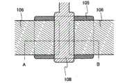
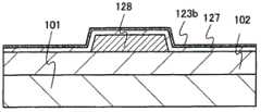
在本实施方式中,将参照图1A和1B和图2A至2C描述绝缘表面上的氧化物半导体膜用作沟道的晶体管及其制造方法。图1B为示出作为半导体装置结构的一实施方式的晶体管结构的截面图,并相当于沿图1A(其为俯视图)中的点虚线A-B的截面图。注意,在图1A中,并未示出衬底101、氧化物绝缘膜102、栅极绝缘膜107以及绝缘膜109。图2A至2C为示出图1B所示的晶体管的制造工序的截面图。In this embodiment mode, a transistor in which an oxide semiconductor film on an insulating surface serves as a channel and a method of manufacturing the same will be described with reference to FIGS. 1A and 1B and FIGS. 2A to 2C . FIG. 1B is a cross-sectional view showing a transistor structure as one embodiment of a semiconductor device structure, and corresponds to a cross-sectional view along a dotted line A-B in FIG. 1A (which is a plan view). Note that in FIG. 1A ,
图1B所示的晶体管包括形成在衬底101上的氧化物绝缘膜102;形成在氧化物绝缘膜102上的氧化物半导体叠层105;形成在氧化物半导体叠层105上并用作源电极和漏电极的一对电极106;形成在氧化物绝缘膜102、氧化物半导体叠层105以及一对电极106上的栅极绝缘膜107;以及隔着栅极绝缘膜107与氧化物半导体叠层105重叠的栅电极108。此外,可以设置覆盖栅极绝缘膜107和栅电极108的绝缘膜109。The transistor shown in FIG. 1B includes an
氧化物半导体叠层105的特征在于层叠有具有第一晶体结构的氧化物半导体膜105a,其接触氧化物绝缘膜102,及具有第二晶体结构的氧化物半导体膜105b,其接触具有第一晶体结构的氧化物半导体膜105a。The
此外,氧化物半导体叠层105的特征在于使用具有第二晶体结构的氧化物半导体膜105b作为种晶而在具有第一晶体结构的氧化物半导体膜105a中发生晶体生长。Further, the
具有第二晶体结构的氧化物半导体膜105b包括三方晶及/或六方晶。The
换言之,具有第二晶体结构的氧化物半导体膜和具有第一晶体结构的氧化物半导体膜两者都包括三方晶及/或六方晶;因此,可从c轴方向观察到六角形晶格图像。In other words, both the oxide semiconductor film having the second crystal structure and the oxide semiconductor film having the first crystal structure include trigonal crystals and/or hexagonal crystals; therefore, a hexagonal lattice pattern can be observed from the c-axis direction.
注意,具有第一晶体结构的氧化物半导体膜105a和具有第二晶体结构的氧化物半导体膜105b各为非单晶,并非全部在非晶状态中,且包括c轴取向晶体区域。Note that the
接下来,将参照图2A至2C描述制造图1B中的晶体管的方法。Next, a method of manufacturing the transistor in FIG. 1B will be described with reference to FIGS. 2A to 2C.
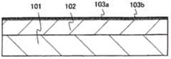
如图2A所示,在于衬底101上形成氧化物绝缘膜102之后,在氧化物绝缘膜102上形成第一氧化物半导体膜103a,并在第一氧化物半导体膜103a上形成第二氧化物半导体膜103b。As shown in FIG. 2A, after the
衬底101需要至少具有够高而足以承受后续的热处理的耐热性。在使用玻璃衬底作为衬底101的情况下,优选使用具有高于或等于730℃的应变点的衬底。作为玻璃衬底的材料,例如,使用铝硅酸玻璃、铝硼硅酸盐玻璃或钡硼硅酸盐玻璃等玻璃材料。注意,优选使用含有BaO及B2O3的玻璃衬底,其中BaO的量大于B2O3的量。针对量产,优选使用第八世代(2160mm×2460mm)、第九世代(2400mm×2800mm或2450mm×3050mm)、第十世代(2950mm×3400mm)等母玻璃作为衬底101。当处理温度很高且处理时间很长时,母玻璃大幅收缩。因此,在使用母玻璃来进行量产的情况下,在工序中,加热温度优选低于或等于600℃,更优选低于或等于450℃。The
除了玻璃衬底以外,还可使用以绝缘体所形成的衬底,如陶瓷衬底、石英衬底或蓝宝石衬底。或者,可使用结晶玻璃等。又或者,可使用通过在诸如硅晶片的半导体衬底的表面或以金属材料制成的导电衬底的表面上形成绝缘膜所得的衬底。In addition to the glass substrate, a substrate formed of an insulator such as a ceramic substrate, a quartz substrate, or a sapphire substrate can also be used. Alternatively, crystallized glass or the like may be used. Still alternatively, a substrate obtained by forming an insulating film on the surface of a semiconductor substrate such as a silicon wafer or the surface of a conductive substrate made of a metal material may be used.
注意,在使用包括杂质(如碱土金属)的玻璃衬底为衬底101的情况下,可在衬底101和氧化物绝缘膜102之间形成诸如氮化硅或氮化铝的氮化物绝缘膜以防止碱土金属的进入。可通过CVD法、溅射法等形成氮化物绝缘膜。由于诸如锂、钠或钾的碱土金属为后续将形成的氧化物半导体膜的杂质,这种碱土金属的含量优选为小。Note that in the case of using a glass substrate including impurities such as alkaline earth metals as the
使用氧化物绝缘膜(自其经加热释放出一部分所含的氧)来形成氧化物绝缘膜102。自其经加热释放出一部分所含的氧的氧化物绝缘膜优选为其氧含量超过化学计量组成的氧化物绝缘膜。通过使用自其经加热释放出一部分所含的氧的氧化物绝缘膜,可经加热将氧扩散到第一氧化物半导体膜103a及第二氧化物半导体膜103b中。氧化物绝缘膜102的典型例子包括氧化硅、氧氮化硅、氮氧化硅、氧化铝、氧氮化铝、氧化镓、氧化铪以及氧化钇。The
从其氧含量超过化学计量组成的氧化物绝缘膜,经加热释放出一部分的氧。在热脱附谱(TDS)分析中,此时所释放且被换算为氧原子的氧量大于或等于1.0×10¹⁸atoms/cm3;优选大于或等于1.0×1020atoms/cm3;更优选大于或等于3.0×1020atoms/cm3。From the oxide insulating film whose oxygen content exceeds the stoichiometric composition, part of the oxygen is released by heating. In thermal desorption spectrum (TDS) analysis, the amount of oxygen released at this time and converted to oxygen atoms is greater than or equal to 1.0×10¹⁸ atoms/cm3 ; preferably greater than or equal to 1.0×10²⁰ atoms/cm3 ; more It is preferably greater than or equal to 3.0×10²⁰ atoms/cm3 .
在此,将描述使用TDS分析来测量被换算为氧原子的氧释放量的方法。Here, a method of measuring the released amount of oxygen converted into oxygen atoms using TDS analysis will be described.
TDS分析中的气体释放量与质谱的积分值成正比。因此,可从氧化物绝缘膜的质谱的积分值相对于标准样品的参考值的比例来计算气体释放量。标准样品的参考值是指样品中所含的预定原子的密度相对于质谱的积分值的比例。The amount of gas released in TDS analysis is proportional to the integrated value of the mass spectrum. Therefore, the gas release amount can be calculated from the ratio of the integrated value of the mass spectrum of the oxide insulating film to the reference value of the standard sample. The reference value of the standard sample refers to the ratio of the density of predetermined atoms contained in the sample to the integrated value of the mass spectrum.
例如,可根据算式1通过利用包含预定密度的氢的硅晶片(其为标准样品)的TDS分析结果及氧化物绝缘膜的TDS分析结果求出从氧化物绝缘膜释放的氧分子量(N(O2))。在此假设:具有由TDS分析所得的质量数32的所有质谱都源自氧分子。在CH3OH不大可能存在的前提下,不考虑其质量数为32的气体的CH3OH。此外,也不考虑包括其质量数为17或18的氧原子的氧分子(其为氧原子的同位素),因为在自然世界中这种分子的比例很小。For example, the molecular weight of oxygen released from the oxide insulating film (N(O2 )). It is assumed here that all mass spectra with mass number 32 obtained by TDS analysis originate from oxygen molecules. On the premise that CH3 OH is unlikely to exist, the CH3 OH of the gas whose mass number is 32 is not considered. In addition, oxygen molecules including oxygen atoms with mass numbers 17 or 18 (which are isotopes of oxygen atoms) are also not considered because the proportion of such molecules in the natural world is small.
N(O2)=N(H2)/S(H2)×S(O2)×α (算式1)N(O2 )=N(H2 )/S(H2 )×S(O2 )×α (Equation 1)
N(H2)为通过将从标准样品释放的氢分子数量换算为密度所得的值。S(H2)为当由TDS分析标准样品时的质谱的积分值。在此,将标准样品的参考值设定为N(H2)/S(H2)。S(O2)为当通过TDS分析氧化物绝缘膜时的质谱的积分值。α为影响TDS分析中的质谱强度的系数。算式1的细节可参照日本专利申请公开H6-275697号公报。注意,以由ESCO Ltd.制造的EMD-WA1000S/W的热脱附谱设备使用包含1×1016atoms/cm3的氢原子的硅晶片作为标准样品来测量从氧化物绝缘膜所释放出的氧量。N(H2 ) is a value obtained by converting the number of hydrogen molecules released from a standard sample into density. S(H2 ) is the integrated value of the mass spectrum when the standard sample is analyzed by TDS. Here, the reference value of the standard sample is set as N(H2 )/S(H2 ). S(O2 ) is an integral value of a mass spectrum when an oxide insulating film is analyzed by TDS. α is a coefficient affecting the mass spectrum intensity in TDS analysis. For details of the
此外,在TDS分析中,将一部分的氧作为氧原子检测。可从氧分子的离子化速率计算氧分子与氧原子之间的比例。注意,由于上述α包括氧分子的离子化速率,所以可经氧分子释放量的评估来估计氧原子释放量。In addition, in TDS analysis, a part of oxygen is detected as an oxygen atom. The ratio between oxygen molecules and oxygen atoms can be calculated from the ionization rate of oxygen molecules. Note that since the above α includes the ionization rate of oxygen molecules, the amount of released oxygen atoms can be estimated from the evaluation of the released amount of oxygen molecules.
注意,N(O2)为氧分子释放量。关于氧化物绝缘膜,在换算为氧原子的氧释放量为氧分子释放量的两倍。Note that N(O2 ) is the released amount of oxygen molecules. With regard to the oxide insulating film, the released amount of oxygen in terms of oxygen atoms is twice the released amount of oxygen molecules.
氧化物绝缘膜102的厚度大于或等于50nm,优选大于或等于200nm且小于或等于500nm。通过使用厚的氧化物绝缘膜102,可增加从氧化物绝缘膜102释放出的氧量,并且可减少在氧化物绝缘膜102与后续形成的氧化物半导体膜之间的界面的缺陷。The thickness of the
通过溅射法、CVD法等来形成氧化物绝缘膜102。优选地,通过溅射法容易形成通过热处理从其释放所包含的氧的一部分的氧化物绝缘膜。The
在利用溅射法形成通过热处理从其释放所包含的氧的一部分的氧化物绝缘膜时,沉积气体中的氧量优选很大,且可使用氧、氧和稀有气体的混合气体等。典型地,沉积气体中的氧浓度优选高于或等于6%且低于或等于100%。When forming an oxide insulating film from which part of contained oxygen is released by heat treatment by sputtering, the amount of oxygen in the deposition gas is preferably large, and oxygen, a mixed gas of oxygen and a rare gas, or the like can be used. Typically, the oxygen concentration in the deposition gas is preferably higher than or equal to 6% and lower than or equal to 100%.
使用可经加热包括三方晶及/或六方晶并具有第一晶体结构的氧化物半导体膜来形成第一氧化物半导体膜103a。The first
作为第一氧化物半导体膜103a,可使用诸如In-Sn-Ga-Zn-O膜的四元金属氧化物;诸如In-Ga-Zn-O膜、In-Sn-Zn-O膜、In-Al-Zn-O膜、Sn-Ga-Zn-O膜、Al-Ga-Zn-O膜或Sn-Al-Zn-O膜的三元金属氧化物;诸如In-Zn-O膜、Sn-Zn-O膜、Al-Zn-O膜或In-Ga-O膜的二元金属氧化物等。此外,SiO2可包含在上述氧化物半导体中。在本说明书中,例如,In-Ga-Zn-O膜是指含有铟(In)、镓(Ga)以及锌(Zn)的氧化物膜。As the first
使用可经加热包括三方晶及/或六方晶并具有非纤锌矿结构、YbFe2O4结构、Yb2Fe3O7结构以及前述结构的变形结构中的任一晶体结构的氧化物半导体膜来形成第一氧化物半导体膜103a。An oxide semiconductor film that can be heated includes trigonal and/orhexagonal crystals and has any crystal structure among non-wurtzite structure,YbFe2O4 structure,Yb2Fe3O7 structure, andmodified structures of the foregoing structures. to form the first
作为具有第一晶体结构的氧化物半导体膜的一个例子,为三元金属氧化物的In-Ga-Zn-O膜包括三角及/或六角形非纤锌矿晶体。另外,为三元金属氧化物的In-Ga-Zn-O膜的例子包括具有YbFe2O4结构的InGaZnO4及具有Yb2Fe3O7结构的In2Ga2ZnO7,且In-Ga-Zn-O膜可具有前述结构的变形结构(M.Nakamura,N.Kimizuka,and T.Mohri,“The Phase Relations in the In2O3-Ga2ZnO4-ZnO System at1350℃(In2O3-Ga2ZnO4-ZnO系在1350℃下的相位关系)”,J.Solid StateChem.,1991,Vol.93,pp.298-315)。注意,以下含有Yb的层以A层表示且含有Fe的层以B层表示。YbFe2O4结构为ABB|ABB|ABB的重复结构。作为YbFe2O4结构的变形结构之一个例子,可举出ABBB|ABBB的重复结构。此外,Yb2Fe3O7结构为ABB|AB|ABB|AB的重复结构。作为Yb2Fe3O7结构的变形结构之一个例子,可举出ABBB|ABB|ABBB|ABB|ABBB|ABB的重复结构。As an example of the oxide semiconductor film having the first crystal structure, an In—Ga—Zn—O film that is a ternary metal oxide includes triangular and/or hexagonal non-wurtzite crystals. In addition, examples of In-Ga-Zn-O films that are ternary metal oxides include InGaZnO4 having a YbFe2 O4 structure and In2 Ga2 ZnO7 having a Yb2 Fe3 O7 structure, and In-Ga The -Zn-O film may have a deformed structure of the aforementioned structure (M. Nakamura, N. Kimizuka, and T. Mohri, "The Phase Relations in the In2 O3 -Ga2 ZnO4 -ZnO System at 1350°C (In2 O3 -Ga2 ZnO4 -ZnO phase relationship at 1350°C), ", J.Solid State Chem., 1991, Vol.93, pp.298-315). Note that, below, a layer containing Yb is represented by A layer and a layer containing Fe is represented by B layer. The structure of YbFe2 O4 is a repeating structure of ABB|ABB|ABB. As an example of a deformed structure of the YbFe2 O4 structure, a repeating structure of ABBB|ABBB is mentioned. In addition, the structure of Yb2 Fe3 O7 is a repeating structure of ABB|AB|ABB|AB. As an example of a modified structure of the Yb2 Fe3 O7 structure, there is a repeating structure of ABBB|ABB|ABBB|ABB|ABBB|ABB.
注意,也可以使用含有高于或等于1×10¹⁷/cm3且低于5×1019/cm3的浓度的氮的上述金属氧化物作为第一氧化物半导体膜103a。Note that the above-described metal oxide containing nitrogen at a concentration higher than or equal to 1×10¹⁷ /cm3 and lower than 5×10¹⁹ /cm3 may also be used as the first
注意,可形成第一氧化物半导体膜103a的金属氧化物的能隙为2eV或更大;优选为2.5eV或更大;更优选为3eV或更大。依照此方式,可通过使用具有宽能隙的氧化物半导体来减少晶体管的关态电流(off-state current)。Note that the metal oxide that can form the first
使用可经加热具有第二晶体结构的氧化物半导体膜来形成第二氧化物半导体膜103b。可具有第二晶体结构的氧化物半导体膜经热处理而容易结晶,并与可具有三角形及/或六角形第一晶体结构的氧化物半导体膜相比具有更高结晶性。The second
可使用氧化锌、氧氮化物半导体等来形成第二氧化物半导体膜103b。可通过将氮以高于或等于5×10¹⁹/cm3且低于7at.%的浓度添加到作为第一氧化物半导体膜103a举出的任何金属氧化物来得到氧氮化物半导体。The second
使用第二氧化物半导体膜103b作为第一氧化物半导体膜103a的晶体生长的晶种。因此,第二氧化物半导体膜103b可具有能够促进晶体生长的厚度,典型为大于或等于一原子层的厚度且小于或等于10nm,优选大于或等于2nm且小于或等于5nm。在第二氧化物半导体膜103b为薄时,可提高沉积处理及热处理中的处理量。The second
第一氧化物半导体膜103a及第二氧化物半导体膜103b各可通过溅射法、涂敷法、印刷法、脉冲激光蒸镀法等形成。在通过溅射法形成第一氧化物半导体膜103a及第二氧化物半导体膜103b时,使用AC溅射设备、DC溅射设备以及RF溅射设备之一。Each of the first
在通过利用使用氮氧化物半导体的溅射法来形成第二氧化物半导体膜103b时,可通过改变引入到溅射设备的气体的种类,也就是说,通过在形成第一氧化物半导体膜103a之后引入氮,来沉积氮氧化物半导体。换言之,可接续地形成第一氧化物半导体膜103a及第二氧化物半导体膜103b,此具有高生产力。When the second
接下来,进行第一热处理。第一热处理的温度高于或等于150℃且低于或等于650℃,优选高于或等于200℃且低于或等于500℃。另外,第一热处理的加热时间长于或等于1分钟且短于或等于24小时。在逐渐增高第一热处理的温度后,可将温度设为恒定。在从高于或等于500℃的温度升高的速率高于或等于0.5℃/h且低于或等于3℃/h时,逐渐进行第二氧化物半导体膜103b的晶体生长;因此,可进一步增高结晶性。Next, the first heat treatment is performed. The temperature of the first heat treatment is higher than or equal to 150°C and lower than or equal to 650°C, preferably higher than or equal to 200°C and lower than or equal to 500°C. In addition, the heating time of the first heat treatment is longer than or equal to 1 minute and shorter than or equal to 24 hours. After gradually increasing the temperature of the first heat treatment, the temperature can be made constant. The crystal growth of the second
优选在稀有气体(典型为氩)气氛、氧气氛、氮气氛、干空气气氛、稀有气体(典型为氩)和氧的混合气氛或稀有气体和氮的混合气氛中进行第一热处理。具体来说,优选使用高纯度气体气氛,其中诸如氢的杂质的浓度减少至大约百万分之几(ppm)或十亿分之几(ppb)。The first heat treatment is preferably performed in a rare gas (typically argon) atmosphere, an oxygen atmosphere, a nitrogen atmosphere, a dry air atmosphere, a mixed atmosphere of a rare gas (typically argon) and oxygen, or a mixed atmosphere of a rare gas and nitrogen. Specifically, it is preferable to use a high-purity gas atmosphere in which the concentration of impurities such as hydrogen is reduced to about parts per million (ppm) or parts per billion (ppb).
用于第一热处理的热处理设备不限于特定设备,且该设备可具备用于经来自加热元件(如电阻式加热元件)的热辐射或热传导加热待处理物体的装置。例如,可使用电炉,或诸如气体快速热退火(GRTA)设备或灯快速热退火(LRTA)设备的快速热退火(RTA)设备。LRTA设备为以从诸如卤素灯、金属卤化物、氙弧灯、碳弧灯、高压钠灯或高压汞灯的灯所发射的光的辐射(电磁波)加热待处理物体的设备。GRTA设备为用于利用高温气体的热处理的设备。The heat treatment apparatus used for the first heat treatment is not limited to a specific apparatus, and the apparatus may be provided with means for heating the object to be treated via heat radiation or heat conduction from a heating element such as a resistance heating element. For example, an electric furnace, or rapid thermal annealing (RTA) equipment such as gas rapid thermal annealing (GRTA) equipment or lamp rapid thermal annealing (LRTA) equipment may be used. The LRTA apparatus is an apparatus that heats an object to be treated with radiation (electromagnetic waves) of light emitted from a lamp such as a halogen lamp, metal halide, xenon arc lamp, carbon arc lamp, high-pressure sodium lamp, or high-pressure mercury lamp. The GRTA equipment is equipment used for heat treatment using high-temperature gas.
通过进行第一热处理,使晶体生长从第二氧化物半导体膜103b的表面朝第一氧化物半导体膜103a开始。由于第二氧化物半导体膜103b容易结晶,所以整个第二氧化物半导体膜103b结晶而成为具有第二晶体结构的氧化物半导体膜104b。此外,由于晶体生长从第二氧化物半导体膜103b的表面朝第一氧化物半导体膜103a进行,形成c轴取向的晶体区域。也就是说,具有第二晶体结构的氧化物半导体膜104b包括在a-b面中的上平面中形成六角形的键。另外,包括六角形键的层在厚度方向(c轴方向)上层叠并键合,而得到c轴取向。By performing the first heat treatment, crystal growth starts from the surface of the second
在继续进行第一热处理时,以具有第二晶体结构的氧化物半导体膜104b作为晶种,第一氧化物半导体膜103a的晶体生长从与具有第二晶体结构的氧化物半导体膜104b的界面朝氧化物绝缘膜102继续进行。具有第二晶体结构的氧化物半导体膜104b的晶体在c轴方向上取向,由此通过使用具有第二晶体结构的氧化物半导体膜104b作为晶种,第一氧化物半导体膜103a中的晶体可生长而变成与具有第二晶体结构的氧化物半导体膜104b的晶轴大致上对准。也就是说,第一氧化物半导体膜103a中的晶体可在对准c轴的同时生长。也就是说,具有第一晶体结构的氧化物半导体膜104a包括在a-b面中的上平面中形成六角形的键。另外,包括六角形键的层在厚度方向(c轴方向)上层叠并键合,而得到c轴取向。经上述步骤,可形成具有c轴取向的第一晶体结构的氧化物半导体膜104a(参照图2B)。When the first heat treatment is continued, with the
在经第一热处理晶体生长从第二氧化物半导体膜103b的表面垂直进行的情况下,具有第一晶体结构的氧化物半导体膜104a及具有第二晶体结构的氧化物半导体膜104b的c轴与该表面大致上垂直。In the case where the crystal growth proceeds vertically from the surface of the second
另外,经第一热处理,释放出包含在第一氧化物半导体膜103a及第二氧化物半导体膜103b中的氢(也就是说,发生脱氢或脱水)且包含在氧化物绝缘膜102中的氧的一部分扩散到第一氧化物半导体膜103a、第二氧化物半导体膜103b以及氧化物绝缘膜102的一区域(其与第一氧化物半导体膜103a的界面附近)。通过此步骤,可减少包含在第一氧化物半导体膜103a及第二氧化物半导体膜103b中的氧缺陷;此外,通过将氧扩散到第一氧化物半导体膜103a附近的氧化物绝缘膜102的区域,可以减少在氧化物绝缘膜102与第一氧化物半导体膜103a之间的界面的缺陷。结果,可形成其中氢浓度及氧缺陷已减少的具有第一晶体结构的氧化物半导体膜104a及具有第二晶体结构的氧化物半导体膜104b。In addition, through the first heat treatment, hydrogen contained in the first
通过在以溅射法形成第一氧化物半导体膜103a和第二氧化物半导体膜103b时将溅射设备的处理室的泄漏率设定成1×10⁻¹⁰Pa□m3/s或更低,可在利用溅射法的成膜期间中抑制如碱金属或氢的杂质进入到第一氧化物半导体膜103a及第二氧化物半导体膜103b中。此外,使用捕集真空泵(例如,低温泵)作为抽空系统,可减少来自抽空系统的如碱金属或氢的杂质的逆流。By setting the leak rate of the processing chamber of the sputtering apparatus to 1×10⁻¹⁰ Pa m3 /s or lower when the first
此外,可在加热了引入到溅射设备的处理室内的气体(诸如氮气、氧气或氩气)的状态下形成第一氧化物半导体膜103a及第二氧化物半导体膜103b。因此,可减少第一氧化物半导体膜103a及第二氧化物半导体膜103b中的氢含量。In addition, the first
此外,在通过溅射法形成第一氧化物半导体膜103a及第二氧化物半导体膜103b之前,进行预热处理以去除溅射设备或靶材表面或内部所含的湿气或氢。因此,可减少第一氧化物半导体膜103a及第二氧化物半导体膜103b中的氢含量。In addition, before forming the first
经上述步骤,可形成具有第一晶体结构的氧化物半导体膜104a及具有第二晶体结构的氧化物半导体膜104b。若氢包含在氧化物半导体中,其部分用作施体而产生电子作为载流子。另外,氧化物半导体中的氧缺陷也用作施体而产生电子作为载流子。因此,当在具有第一晶体结构的氧化物半导体膜104a及具有第二晶体结构的氧化物半导体膜104b中减少氢浓度及氧缺陷时,可减少氧化物半导体中的载流子浓度,并可抑制后续将制造的晶体管的阈值电压的负偏移。Through the above steps, the
<六方晶结构><Hexagonal crystal structure>
在此,以下描述六方晶结构。Here, the hexagonal crystal structure is described below.
首先,将参照图3A及3B描述c轴取向的第二晶体结构。针对c轴取向的第二晶体结构,图3A示出从c轴方向看到的a-b面中的结构,且图3B示出其中c轴方向为垂直方向的结构。First, the second crystal structure of the c-axis orientation will be described with reference to FIGS. 3A and 3B . Regarding the second crystal structure of the c-axis orientation, FIG. 3A shows a structure in the a-b plane viewed from the c-axis direction, and FIG. 3B shows a structure in which the c-axis direction is a vertical direction.
具有第二晶体结构的晶体的例子包括氧化锌、氮化铟以及氮化镓。此外,含氮的氧化物半导体,也就是说,氧氮化物半导体,在某些情况下可以为具有c轴取向的第二晶体结构的膜。Examples of crystals having the second crystal structure include zinc oxide, indium nitride, and gallium nitride. In addition, a nitrogen-containing oxide semiconductor, that is, an oxynitride semiconductor may be a film having a second crystal structure of c-axis orientation in some cases.
具体来说,含有其浓度高于或等于5×10¹⁹/cm3,优选高于或等于1×1020/cm3且低于20at.%的氮的In-Ga-Zn-O膜成为具有c轴取向的第二晶体结构的膜,且具有在In-O晶面(含有铟及氧的晶面)与另一个In-O晶面(含有铟及氧的晶面)之间含有Ga及Zn的一层。Specifically, an In-Ga-Zn-O film containing nitrogen at a concentration higher than or equal to 5×10¹⁹ /cm3 , preferably higher than or equal to 1×10²⁰ /cm3 and lower than 20 at.% becomes a film having A film of the second crystal structure of the c-axis orientation, and has Ga and A layer of Zn.
接下来,将描述c轴取向的六方晶的第一晶体结构。Next, the first crystal structure of c-axis-oriented hexagonal crystals will be described.
例如,含有其浓度高于或等于1×10¹⁷/cm3且低于5×1019/cm3的氮的In-Ga-Zn-O膜成为具有c轴取向的六方晶的第一晶体结构的膜。具有c轴取向的六方晶的第一晶体结构的In-Ga-Zn-O膜在a-b面中具有In-O晶面(含有铟及氧的晶面)及在In-O晶面之间含有Ga及Zn的两层。注意,针对含有Ga及Zn的两层,对Ga及Zn的位置并无限制,只要Ga及Zn中的至少一个包含在每一层中。For example, an In-Ga-Zn-O film containing nitrogen whose concentration is higher than or equal to 1×10¹⁷ /cm3 and lower than 5×10¹⁹ /cm3 becomes the first crystal structure of hexagonal crystal with c-axis orientation membrane. The In-Ga-Zn-O film having the first crystal structure of c-axis oriented hexagonal crystal has In-O crystal planes (crystal planes containing indium and oxygen) in the ab plane and contains Two layers of Ga and Zn. Note that for two layers containing Ga and Zn, there is no limitation on the positions of Ga and Zn as long as at least one of Ga and Zn is contained in each layer.
第二晶体结构及第一晶体结构两者都为六方晶结构,其中原子在a-b面中配置为六角形形状。此外,六方晶的第一晶体结构接触第二晶体结构,且六方晶的第一晶体结构与第二晶体结构对准。Both the second crystal structure and the first crystal structure are hexagonal crystal structures in which atoms are arranged in a hexagonal shape in the a-b plane. In addition, the first crystal structure of the hexagonal crystal contacts the second crystal structure, and the first crystal structure of the hexagonal crystal is aligned with the second crystal structure.
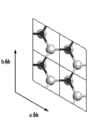
图4A至4C示出c轴取向的六方晶的第二晶体结构在具有同一晶格常数的c轴取向的第一晶体结构上对准的方式。图4A示出c轴取向的六方晶的第二晶体结构2000,且图4B示出c轴取向的第一晶体结构2001。另外,图4C为示出六方晶的第二晶体结构2000接触第一晶体结构2001且六方晶的第一晶体结构2001与第二晶体结构2000对准的方式的示意图。4A to 4C illustrate the manner in which a c-axis oriented hexagonal second crystal structure is aligned on a c-axis oriented first crystal structure having the same lattice constant. FIG. 4A shows a c-axis-oriented hexagonal
依照此方式,六方晶的第一晶体结构2001接触第二晶体结构2000且六方晶的第一晶体结构2001与第二晶体结构2000对准。也就是说,形成包括c轴取向的第二晶体结构2000(其具有高结晶性且容易加以结晶)的层作为种晶层,并形成接触种晶层的氧化物半导体膜,由此包括在种晶层中的第二晶体结构2000促进氧化物半导体膜的结晶。In this way, the hexagonal
<种晶层><seed layer>
接下来,将描述种晶层。种晶层包括c轴取向的第二晶体结构。尤其,使用与氧化物半导体膜相比具有更高结晶性且更容易加以结晶的材料来形成种晶层。Next, the seed layer will be described. The seed layer includes a c-axis oriented second crystal structure. In particular, the seed layer is formed using a material that has higher crystallinity and is more easily crystallized than an oxide semiconductor film.
以下描述可应用于种晶层的c轴取向的第二晶体结构。The second crystal structure applicable to the c-axis orientation of the seed layer is described below.
作为具有c轴取向的第二晶体结构并可用于种晶层的化合物的例子,可举出氧化锌、氮化铟以及氮化镓。含有其浓度高于或等于5×10¹⁹/cm3(优选高于或等于1×1020/cm3且低于7at.%)的氮的氧化物半导体可在某些情况下为包括c轴取向的第二晶体结构的膜。Examples of the compound having the second crystal structure of the c-axis orientation and used for the seed layer include zinc oxide, indium nitride, and gallium nitride. An oxide semiconductor containing nitrogen at a concentration higher than or equal to 5×10¹⁹ /cm3 (preferably higher than or equal to 1×10²⁰ /cm3 and lower than 7 at.%) may include c-axis in some cases Oriented films of the second crystal structure.
在使用含氮的氧化物半导体作为种晶层的情况下,故意使氧化物半导体包含氮以使其氮浓度成为高于或等于5×10¹⁹/cm3,优选高于或等于1×1020/cm3且低于7at.%。故意含有此范围中的氮的氧化物半导体膜具有比故意不含有氮的氧化物半导体膜更小的能隙,并因此容易流入载流子。In the case of using a nitrogen-containing oxide semiconductor as a seed layer, the oxide semiconductor is intentionally made to contain nitrogen so that its nitrogen concentration becomes higher than or equal to 5×10¹⁹ /cm3 , preferably higher than or equal to 1×10²⁰ /cm3 and lower than 7at.%. An oxide semiconductor film intentionally containing nitrogen in this range has a smaller energy gap than an oxide semiconductor film intentionally not containing nitrogen, and thus easily flows carriers.
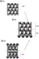
注意,可在c轴取向的第二晶体结构的观察图像中观察到亮点交替出现的衍射图像,该观察图像使用高角度环形暗场(HAADF)-STEM而得。Note that a diffraction image in which bright spots appear alternately can be observed in an observation image of the c-axis-oriented second crystal structure obtained using a high-angle annular dark field (HAADF)-STEM.
图5A示出通过基于c轴取向的第二晶体结构的计算而得的HAADF-STEM观察图像。FIG. 5A shows a HAADF-STEM observation image obtained by calculation based on the second crystal structure of the c-axis orientation.
图5B示出使用仅含有氮的沉积气体所形成的In-Ga-Zn-O膜的HAADF-STEM观察图像。FIG. 5B shows a HAADF-STEM observation image of an In—Ga—Zn—O film formed using a deposition gas containing only nitrogen.
从图5A及5B中的各个HAADF-STEM观察图像,可证实c轴取向的第二晶体结构具有两周期层结构。From the respective HAADF-STEM observation images in FIGS. 5A and 5B , it can be confirmed that the c-axis-oriented second crystal structure has a two-period layer structure.
注意,利用溅射法在石英玻璃衬底上形成300nm厚的含有氮的In-Ga-Zn-O膜。在下列条件下进行沉积:使用含有1:1:1[原子比]的In、Ga以及Zn的靶材;衬底与靶材之间的距离为60mm;使用DC电源;功率为0.5kW;且压力为0.4Pa。沉积期间的衬底温度为400℃,且以40sccm的流速仅将氮作为溅射气体引入到沉积室中。Note that a 300 nm-thick In-Ga-Zn-O film containing nitrogen was formed on a quartz glass substrate by a sputtering method. Deposition was performed under the following conditions: using a target containing In, Ga, and Zn of 1:1:1 [atomic ratio]; a distance between the substrate and the target of 60 mm; using a DC power supply; power of 0.5 kW; and The pressure is 0.4 Pa. The substrate temperature during deposition was 400° C., and only nitrogen was introduced into the deposition chamber as sputtering gas at a flow rate of 40 sccm.
<氧化物半导体膜><Oxide semiconductor film>
接下来,将描述氧化物半导体膜。氧化物半导体膜为非单晶,并非全部在非晶状态中。氧化物半导体膜包括至少c轴取向六方晶的第一晶体结构和从种晶层各向异性生长的晶体。由于氧化物半导体膜并非全部在非晶状态中,抑制非晶部分(其特性不稳定)的形成。Next, the oxide semiconductor film will be described. The oxide semiconductor film is non-single crystal, and not all are in an amorphous state. The oxide semiconductor film includes at least a first crystal structure of c-axis-oriented hexagonal crystals and crystals anisotropically grown from a seed layer. Since the oxide semiconductor film is not entirely in an amorphous state, formation of an amorphous portion (whose characteristics are unstable) is suppressed.
将描述可应用到氧化物半导体膜的具有各向异性的c轴取向第一晶体结构。A c-axis-oriented first crystal structure having anisotropy applicable to an oxide semiconductor film will be described.
作为六方晶的第一晶体结构的例子,可举出YbFe2O4结构、Yb2Fe3O7结构以及前述结构的变形结构。例如,为三元金属氧化物的In-Ga-Zn-O具有六方晶的第一晶体结构并可用于氧化物半导体膜。注意,可用作氧化物半导体膜的In-Ga-Zn-O膜可含有其浓度高于或等于1×10¹⁷/cm3且低于或等于5×1019/cm3的氮。Examples of the first crystal structure of the hexagonal crystal include a YbFe2 O4 structure, a Yb2 Fe3 O7 structure, and modified structures of the aforementioned structures. For example, In-Ga-Zn-O, which is a ternary metal oxide, has a hexagonal first crystal structure and can be used for an oxide semiconductor film. Note that an In-Ga-Zn-O film usable as an oxide semiconductor film may contain nitrogen at a concentration higher than or equal to 1×10¹⁷ /cm3 and lower than or equal to 5×10¹⁹ /cm3 .
为三元金属氧化物的In-Ga-Zn-O的例子包括具有YbFe2O4结构的InGaZnO4及具有Yb2Fe3O7结构的In2Ga2ZnO7,且In-Ga-Zn-O可具有前述结构的变形结构中的任一结构,其公开在下列文献中:M.Nakamura,N.Kimizuka,and T.Mohri,“The Phase Relations in theIn2O3-Ga2ZnO4-ZnO System at1350℃(In2O3-Ga2ZnO4-ZnO系在1350℃下的相位关系)”,J.Solid State Chem.,1991,Vol.93,pp.298-315。Examples of In-Ga-Zn-O which is a ternary metal oxide include InGaZnO4 having a YbFe2 O4 structure and In2 Ga2 ZnO7 having a Yb2 Fe3 O7 structure, and In-Ga-Zn- O may have any one of modified structures of the aforementioned structures, which are disclosed in the following documents: M. Nakamura, N. Kimizuka, and T. Mohri, "The Phase Relations in the In2 O3 -Ga2 ZnO4 -ZnO System at 1350°C (Phase relationship of In2 O3 -Ga2 ZnO4 -ZnO system at 1350°C)", J.Solid State Chem., 1991, Vol.93, pp.298-315.
此外,作为氧化物半导体膜,可使用诸如In-Sn-Ga-Zn-O膜的四元金属氧化物;诸如In-Ga-Zn-O膜、In-Sn-Zn-O膜、In-Al-Zn-O膜、Sn-Ga-Zn-O膜、Al-Ga-Zn-O膜或Sn-Al-Zn-O膜的三元金属氧化物;诸如In-Zn-O膜、Sn-Zn-O膜、Al-Zn-O膜或In-Ga-O膜的二元金属氧化物等。此外,硅可包含在上述氧化物半导体膜中。在本说明书中,例如,In-Ga-Zn-O膜是指含有铟(In)、镓(Ga)以及锌(Zn)的氧化物膜。In addition, as the oxide semiconductor film, a quaternary metal oxide such as an In-Sn-Ga-Zn-O film; such as an In-Ga-Zn-O film, an In-Sn-Zn-O film, an In-Al - Zn-O film, Sn-Ga-Zn-O film, Al-Ga-Zn-O film or ternary metal oxide of Sn-Al-Zn-O film; such as In-Zn-O film, Sn-Zn -O film, binary metal oxide of Al-Zn-O film or In-Ga-O film, etc. In addition, silicon may be contained in the above-mentioned oxide semiconductor film. In this specification, for example, an In—Ga—Zn—O film refers to an oxide film containing indium (In), gallium (Ga), and zinc (Zn).
在该氧化物半导体膜中的晶体从种晶层各向异性生长。据此,具有异质结构的半导体膜的高度结晶区域可接触绝缘表面,并可减少因悬挂键导致的界面态,所以可提供具有异质结构及良好的界面状态的半导体膜。Crystals in this oxide semiconductor film grow anisotropically from the seed layer. Accordingly, a highly crystalline region of a semiconductor film having a heterostructure can contact an insulating surface, and interface states due to dangling bonds can be reduced, so a semiconductor film having a heterostructure and a good interface state can be provided.
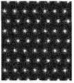
注意,在c轴取向的六方晶的第一晶体结构的观察图像中可观察到每三个点出现一个亮点的衍射图案,其用高角度环形暗场(HAADF)-STEM而得。Note that in the observed image of the first crystal structure of the c-axis oriented hexagonal crystal, a diffraction pattern in which a bright spot appears every three points can be observed, which was obtained with a high-angle annular dark field (HAADF)-STEM.
图6A示出通过基于c轴取向的六方晶的第一晶体结构的计算而得的HAADF-STEM观察图像。FIG. 6A shows a HAADF-STEM observation image obtained by calculation based on a first crystal structure of a c-axis-oriented hexagonal crystal.
图6B示出In-Ga-Zn-O膜的HAADF-STEM观察图像。FIG. 6B shows a HAADF-STEM observation image of the In-Ga-Zn-O film.
从图6A及6B中的各个HAADF-STEM观察图像,可证实每三个点出现一个亮点且c轴取向的六方晶的第一晶体结构具有九周期层结构。From each of the HAADF-STEM observation images in FIGS. 6A and 6B , it was confirmed that a bright spot appeared every three points and that the first crystal structure of the c-axis-oriented hexagonal crystal had a nine-period layer structure.
注意,通过溅射法在石英玻璃衬底上形成300nm厚的In-Ga-Zn-O膜。在下列条件下进行沉积:使用含有1:1:1[原子比]的In、Ga以及Zn的靶材;衬底与靶材之间的距离为60mm;使用DC电源;功率为0.5kW;且压力为0.4Pa。沉积期间的衬底温度为400℃,且以40sccm的流速仅将氧作为溅射气体引入到沉积室中。Note that a 300 nm-thick In-Ga-Zn-O film was formed on a quartz glass substrate by a sputtering method. Deposition was performed under the following conditions: using a target containing In, Ga, and Zn of 1:1:1 [atomic ratio]; a distance between the substrate and the target of 60 mm; using a DC power supply; power of 0.5 kW; and The pressure is 0.4 Pa. The substrate temperature during deposition was 400° C., and only oxygen was introduced into the deposition chamber as a sputtering gas at a flow rate of 40 sccm.
接下来,在具有第二晶体结构的氧化物半导体膜104b上形成掩模,并接着使用掩模选择性蚀刻具有第一晶体结构的氧化物半导体膜104a及具有第二晶体结构的氧化物半导体膜104b,以形成具有第一晶体结构的氧化物半导体膜105a及具有第二晶体结构的氧化物半导体膜105b。注意,具有第一晶体结构的氧化物半导体膜105a及具有第二晶体结构的氧化物半导体膜105b统称为氧化物半导体叠层105。之后,去除掩模。Next, a mask is formed on the
可适当地经光刻工艺或通过喷墨法、印刷法等形成用于蚀刻具有第一晶体结构的氧化物半导体膜104a及具有第二晶体结构的氧化物半导体膜104b的掩模。另外,可适当地通过湿法蚀刻或干法蚀刻蚀刻具有第一晶体结构的氧化物半导体膜104a及具有第二晶体结构的氧化物半导体膜104b。A mask for etching the
接下来,形成接触氧化物半导体叠层105的一对电极106。接着,在氧化物绝缘膜102、氧化物半导体叠层105以及一对电极106上形成栅极绝缘膜107。之后,在栅极绝缘膜107上形成栅电极108。可在栅极绝缘膜107及栅电极108上形成绝缘膜109(参照图2C)。Next, a pair of
一对电极106用作源电极及漏电极。A pair of
可使用选自铝、铬、铜、钽、钛、钼以及钨的金属元素;含有任何这些金属元素作为成分的合金;含有这些金属元素的组合的合金等来形成一对电极106。此外,可使用选自锰、镁、锆以及铍的一或更多金属元素。另外,一对电极106可具有单层结构或具有两或更多层的叠层结构。例如,可举出含硅的铝膜的单层结构、钛膜层叠于铝膜上的两层结构、钛膜层叠于氮化钛上的两层结构、钨膜层叠于氮化钛上的两层结构、钨膜层叠于氮化钽上的两层结构或钛膜、铝膜以及钛膜以此顺序层叠的三层结构。或者,可使用含有铝及选自钛、钽、钨、钼、铬、钕以及钪的一或更多个元素的膜、合金膜或氮化物膜。在使用铜作为一对电极106的材料的情况下,可提供接触氧化物半导体叠层105的铜-镁-铝合金层,并可层叠接触该铜-镁-铝合金层的铜层。The pair of
可使用诸如氧化铟锡、含氧化钨的氧化铟、含氧化钨的氧化铟锌、含氧化钛的氧化铟、含氧化钛的氧化铟锡、氧化铟锌或添加氧化硅的氧化铟锡的透光导电材料来形成一对电极106。还可采用使用上述透光导电材料及上述金属元素所形成的叠层结构。Transparent materials such as indium tin oxide, indium oxide containing tungsten oxide, indium zinc oxide containing tungsten oxide, indium oxide containing titanium oxide, indium tin oxide containing titanium oxide, indium zinc oxide, or indium tin oxide with silicon oxide can be used. A photoconductive material is used to form a pair of
可通过印刷法或喷墨法来形成一对电极106。或者,在通过溅射法、CVD法、蒸镀法等形成导电膜之后,在导电膜上形成掩模并蚀刻导电膜,并由此形成一对电极106。可通过印刷法、喷墨法或光刻法适当地形成在导电膜上所形成的掩模。The pair of
注意,可以下列方式形成氧化物半导体叠层105及一对电极106。在具有第二晶体结构的氧化物半导体膜104b上形成导电膜之后,使用多级灰度光罩来形成凹凸形状的掩模。使用该掩模来蚀刻具有第一晶体结构的氧化物半导体膜104a、具有第二晶体结构的氧化物半导体膜104b以及导电膜。接着,通过灰化分割该凹凸形状的掩模。使用该分割的掩模来选择性蚀刻导电膜。在此工序中,可减少光罩数量及光刻工艺中的步骤数量。Note that the
可使用氧化硅膜、氧氮化硅膜、氮化硅膜、氮氧化硅膜、氧化铝膜、氧氮化铝膜以及氧化镓膜中的任一种来形成具有单层结构或叠层结构的栅极绝缘膜107。优选栅极绝缘膜107中接触氧化物半导体叠层105的一部分含有氧。更优选使用经加热从其释放所含的氧的氧化物绝缘膜来形成栅极绝缘膜107,这与氧化物绝缘膜102类似。使用氧化硅膜可使氧扩散至氧化物半导体叠层105;因此,可得到良好的特性。Any of silicon oxide film, silicon oxynitride film, silicon nitride film, silicon oxynitride film, aluminum oxide film, aluminum oxynitride film, and gallium oxide film can be used to form a single-layer structure or a stacked layer structure. The
在使用高k材料膜(诸如硅酸铪膜(HfSiOx)、添加有氮的硅酸铪膜(HfSixOyNz)、添加有氮的铝酸铪膜(HfAlxOyNz)、氧化铪膜或氧化钇膜)来形成栅极绝缘膜107时,可减少栅极泄漏电流。此外,可使用一种叠层结构,其中层叠有高k材料膜和氧化硅膜、氧氮化硅膜、氮化硅膜、氮氧化硅膜、氧化铝膜、氧氮化铝膜以及氧化镓膜中的一个或更多。栅极绝缘膜107的厚度优选大于或等于1nm且小于或等于300nm,更优选大于或等于5nm且小于或等于50nm。When using high-k material films (such as hafnium silicate film (HfSiOx ), hafnium silicate film doped with nitrogen (HfSix Oy Nz ), hafnium aluminate film doped with nitrogen (HfAlx Oy Nz ) , hafnium oxide film or yttrium oxide film) to form the
可通过溅射法、CVD法等形成栅极绝缘膜107。The
在形成栅极绝缘膜107之前,可以将氧化物半导体叠层105的表面暴露于诸如氧、臭氧或一氧化二氮的氧化气体的等离子体以加以氧化,由此减少氧缺陷。Before forming the
可使用选自铝、铬、铜、钽、钛、钼以及钨的金属元素;含有这些金属元素中的任一种作为成分的合金;含有这些金属元素的组合的合金等来形成栅电极108。此外,可使用选自锰、镁、锆以及铍的一或更多金属元素。另外,栅电极108可具有单层结构或具有两或更多层的叠层结构。例如,可举出含硅的铝膜的单层结构、其中钛膜层叠于铝膜上的两层结构、其中钛膜层叠于氮化钛膜上的两层结构、其中钨膜层叠于氮化钛膜上的两层结构、其中钨膜层叠于氮化钽膜上的两层结构或其中钛膜、铝膜以及钛膜以此顺序层叠的三层结构。或者,可使用含有铝及选自钛、钽、钨、钼、铬、钕以及钪的一或更多个元素的膜、合金膜或氮化物膜。
可使用诸如氧化铟锡、含氧化钨的氧化铟、含氧化钨的氧化铟锌、含氧化钛的氧化铟、含氧化钛的氧化铟锡、氧化铟锌或添加有氧化硅的氧化铟锡的透光导电材料来形成栅电极108。亦可采用使用上述透光导电材料及上述金属元素所形成的叠层结构。Indium tin oxide, indium oxide containing tungsten oxide, indium zinc oxide containing tungsten oxide, indium oxide containing titanium oxide, indium tin oxide containing titanium oxide, indium zinc oxide, or indium tin oxide added with silicon oxide can be used. A light-transmitting conductive material is used to form the
作为接触栅极绝缘膜的材料层,含氮的In-Ga-Zn-O膜、含氮的In-Sn-O膜、含氮的In-Ga-O膜、含氮的In-Zn-O膜、含氮的Sn-O膜、含氮的In-O膜或金属氮化物的膜(诸如InN或ZnN)优选设置在栅电极108与栅极绝缘膜之间。这些膜各具有5eV或更高的功函数,优选5.5eV或更高;因此,晶体管的电特性的阈值电压可为正。据此,可实现所谓的常关型开关元件。例如,在使用含氮的In-Ga-Zn-O膜的情况下,使用其氮浓度至少高于氧化物半导体叠层105的In-Ga-Zn-O膜;具体来说,使用其氮浓度为7at.%或更高的In-Ga-Zn-O膜。As the material layer contacting the gate insulating film, nitrogen-containing In-Ga-Zn-O film, nitrogen-containing In-Sn-O film, nitrogen-containing In-Ga-O film, nitrogen-containing In-Zn-O film A film, a nitrogen-containing Sn—O film, a nitrogen-containing In—O film, or a film of metal nitride such as InN or ZnN is preferably provided between the
可通过印刷法或喷墨法形成栅电极108。或者,在通过溅射法、CVD法、蒸镀法等形成导电膜之后,在导电膜上形成掩模并蚀刻导电膜,并由此形成栅电极108。可通过印刷法、喷墨法或光刻法适当地形成在导电膜上所形成的掩模。The
可以针对栅极绝缘膜107所列举的任何绝缘膜适当地形成绝缘膜109。当通过溅射法形成氮化硅膜作为绝缘膜109时,可防止湿气及碱金属从外部进入,并因此可减少氧化物半导体叠层105所包括的杂质的数量。The insulating
注意,在形成栅极绝缘膜107或绝缘膜109之后,可在含有很少氢及湿气(以湿气而言,例如,露点低于或等于-40℃,优选低于或等于-60℃)的气氛(诸如氮气氛、氧气氛或干空气气氛)中进行热处理(温度范围:高于或等于150℃且低于或等于650℃,优选高于或等于200℃且低于或等于500℃)。Note that, after forming the
经上述步骤,可制造一种晶体管,其沟道包括氧化物半导体叠层,该氧化物半导体叠层包括在a-b面中具有六角形键的晶体及c轴取向三方晶及/或六方晶结构。Through the above steps, a transistor can be manufactured, the channel of which includes an oxide semiconductor stack including a crystal having a hexagonal bond in the a-b plane and a c-axis oriented trigonal and/or hexagonal crystal structure.
在本实施方式中描述的氧化物半导体叠层在与栅极绝缘膜的界面附近具有高结晶性及均匀性并因此具有稳定的电特性;据此,可得到高可靠性晶体管。包括在a-b面中具有六角形键的晶体及c轴取向三方晶及/或六方晶结构的氧化物半导体叠层用于晶体管的沟道区,由此可制造出其中在晶体管被进行光照射或偏压-温度应力(BT)测试前或后之间的阈值电压的改变量很小且具有稳定的电特性的晶体管。The oxide semiconductor stack described in this embodiment mode has high crystallinity and uniformity near the interface with the gate insulating film and thus has stable electrical characteristics; thereby, a highly reliable transistor can be obtained. An oxide semiconductor stack including a crystal having a hexagonal bond in the a-b plane and a c-axis-oriented trigonal and/or hexagonal crystal structure is used for a channel region of a transistor, thereby making it possible to fabricate a transistor in which the transistor is irradiated with light or A transistor whose threshold voltage changes little before and after a bias-temperature stress (BT) test and has stable electrical characteristics.
实施方式2Embodiment 2
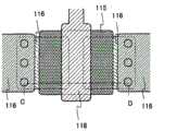
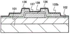
在本实施方式中,将参照图7A及7B及图8A至8C描述与实施方式1不同的晶体管的结构和其制造方法。本实施方式与实施方式1的不同之处在于在氧化物绝缘膜与氧化物半导体叠层之间设置一对电极。注意,图7B相当于沿着图7A(俯视图)中的点虚线C-D的截面图。在图7A中,并未示出衬底101、氧化物绝缘膜102、栅极绝缘膜117以及绝缘膜119。图8A至8C为示出图7B所示的晶体管的制造工序的截面图。In this embodiment mode, the structure of a transistor different from
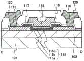
图7B所示的晶体管包括形成在衬底101上的氧化物绝缘膜102;形成在氧化物绝缘膜102上并用作源电极和漏电极的一对电极116;覆盖氧化物绝缘膜102及用作源电极和漏电极的一对电极116的氧化物半导体叠层115;形成在氧化物绝缘膜102、一对电极116以及氧化物半导体叠层115上的栅极绝缘膜117;及隔着栅极绝缘膜117与氧化物半导体叠层115重叠的栅电极118。此外,可设置覆盖栅极绝缘膜117和栅电极118的绝缘膜119。此外,可设置在绝缘膜119的开口中接触一对电极116的一对布线120。The transistor shown in FIG. 7B includes an
氧化物半导体叠层115的特征在于层叠有具有第一晶体结构的氧化物半导体膜115a,其接触氧化物绝缘膜102和一对电极116,及具有第二晶体结构的氧化物半导体膜115b,其接触具有第一晶体结构的氧化物半导体膜115a。The
此外,氧化物半导体叠层115的特征在于使用具有第二晶体结构的氧化物半导体膜115b作为种晶而在具有第一晶体结构的氧化物半导体膜115a中发生晶体生长。Further, the
如同在实施方式1中一样,具有第二晶体结构的氧化物半导体膜及具有第一晶体结构的氧化物半导体膜包括三方晶及/或六方晶;因此,可从c轴方向观察到六角形晶格图像。As in
注意,具有第一晶体结构的氧化物半导体膜115a及具有第二晶体结构的氧化物半导体膜115b各为非单晶,并非全部在非晶状态中,且包括c轴取向晶体。Note that the
接下来,将参照图8A至8C描述制造图7B中的晶体管的方法。Next, a method of manufacturing the transistor in FIG. 7B will be described with reference to FIGS. 8A to 8C.
如图8A所示,如同在实施方式1中一样,在衬底101上形成氧化物绝缘膜102。接着,在氧化物绝缘膜102上形成一对电极116。然后,在一对电极116及氧化物绝缘膜102上形成第一氧化物半导体膜113a及第二氧化物半导体膜113b。As shown in FIG. 8A , as in
可通过使用与在实施方式1中描述的一对电极106的那些类似的材料及形成方法来适当地形成一对电极116。The pair of
可通过使用与在实施方式1中描述的第一氧化物半导体膜103a及第二氧化物半导体膜103b的那些类似的材料及形成方法来适当地形成第一氧化物半导体膜113a及第二氧化物半导体膜113b。The first
接下来,以与实施方式1中的那些类似的方式,进行第一热处理。通过进行第一热处理,使晶体生长从第二氧化物半导体膜113b的表面朝第一氧化物半导体膜113a开始,使得第二氧化物半导体膜113b成为具有第二晶体结构的氧化物半导体膜114b。具有第二晶体结构的氧化物半导体膜114b包括c轴取向晶体。Next, in a manner similar to those in
在继续进行第一热处理时,以具有第二晶体结构的氧化物半导体膜114b作为晶种,第一氧化物半导体膜113a的晶体生长从与具有第二晶体结构的氧化物半导体膜114b的界面朝氧化物绝缘膜102继续进行,以形成具有第一晶体结构的氧化物半导体膜114a。具有第一晶体结构的氧化物半导体膜114a包括c轴取向晶体(参照图8B)。When the first heat treatment is continued, with the
经上述步骤,可形成具有第一晶体结构的氧化物半导体膜114a及具有第二晶体结构的氧化物半导体膜114b。Through the above steps, the
接下来,在具有第二晶体结构的氧化物半导体膜114b上形成掩模,并接着使用该掩模选择性蚀刻具有第一晶体结构的氧化物半导体膜114a及具有第二晶体结构的氧化物半导体膜114b,以形成具有第一晶体结构的氧化物半导体膜115a及具有第二晶体结构的氧化物半导体膜115b。注意,第一晶体结构的氧化物半导体膜115a及具有第二晶体结构的氧化物半导体膜115b统称为氧化物半导体叠层115。之后,去除掩模。Next, a mask is formed on the
接下来,在氧化物绝缘膜102、一对电极116以及氧化物半导体叠层115上形成栅极绝缘膜117。接着,在栅极绝缘膜117上形成栅电极118。Next, a
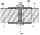
之后,在栅极绝缘膜117及栅电极118上形成绝缘膜119。接着,在绝缘膜119上形成掩模后,部分蚀刻栅极绝缘膜117及绝缘膜119以形成开口。接着,可形成经由该些开口连接到一对电极116的布线120(参照图8C)。After that, an insulating
可通过使用与在实施方式1中描述的栅极绝缘膜107的那些类似的材料及形成方法来适当地形成栅极绝缘膜117。The
可通过使用与在实施方式1中描述的栅电极108的那些类似的材料及形成方法来适当地形成栅电极118。The
可通过使用与在实施方式1中描述的绝缘膜109的那些类似的材料及形成方法来适当地形成绝缘膜119。The insulating
可通过使用与一对电极116的那些类似的材料及形成方法来适当地形成布线120。The
经上述步骤,可制造一种晶体管,其沟道区包括氧化物半导体叠层,该氧化物半导体叠层包括在a-b面中具有六角形键的晶体及c轴取向三方晶及/或六方晶结构。Through the above steps, a transistor can be manufactured, the channel region of which includes an oxide semiconductor stack including a crystal having a hexagonal bond in the a-b plane and a c-axis oriented trigonal and/or hexagonal crystal structure .
在本实施方式中描述的氧化物半导体叠层在与栅极绝缘膜的界面附近具有高结晶性及均匀性并因此具有稳定的电特性;据此,可得到高可靠性晶体管。包括在a-b面中具有六角形键的晶体及c轴取向三方晶及/或六方晶结构的氧化物半导体叠层用于晶体管的沟道区,由此可制造出其中在晶体管被进行光照射或偏压-温度应力(BT)测试前或后之间的阈值电压的改变量很小且具有稳定的电特性的晶体管。The oxide semiconductor stack described in this embodiment mode has high crystallinity and uniformity near the interface with the gate insulating film and thus has stable electrical characteristics; thereby, a highly reliable transistor can be obtained. An oxide semiconductor stack including a crystal having a hexagonal bond in the a-b plane and a c-axis-oriented trigonal and/or hexagonal crystal structure is used for a channel region of a transistor, thereby making it possible to fabricate a transistor in which the transistor is irradiated with light or A transistor whose threshold voltage changes little before and after a bias-temperature stress (BT) test and has stable electrical characteristics.
注意,本实施方式可与其他实施方式中的任一个适当地组合。Note that this embodiment mode can be appropriately combined with any of the other embodiment modes.
实施方式3Embodiment 3
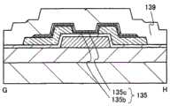
在本实施方式中,将参照图9A及9B及图10A至10E描述使用氧化物半导体膜作为沟道的晶体管和其制造方法。图9B为示出半导体装置的结构之一实施方式的晶体管的结构的截面图,且相当于沿着图9A(俯视图)中的点虚线A-B的截面图。注意,在图9A中,并未示出衬底101、氧化物绝缘膜102、栅极绝缘膜107以及绝缘膜109。图10A至10E为示出图9B所示的晶体管的制造工序的截面图。In this embodiment mode, a transistor using an oxide semiconductor film as a channel and a manufacturing method thereof will be described with reference to FIGS. 9A and 9B and FIGS. 10A to 10E . 9B is a cross-sectional view illustrating the structure of a transistor according to one embodiment of the structure of a semiconductor device, and corresponds to a cross-sectional view along the dotted line A-B in FIG. 9A (top view). Note that, in FIG. 9A ,
图9B所示的晶体管包括形成在衬底101上的氧化物绝缘膜102;形成在氧化物绝缘膜102上的氧化物半导体叠层105、形成在氧化物半导体叠层105上并用作源电极和漏电极的一对电极106;形成在氧化物绝缘膜102、氧化物半导体叠层105以及一对电极106上的栅极绝缘膜107;及隔着栅极绝缘膜107与氧化物半导体叠层105重叠的栅电极108。此外,可设置覆盖栅极绝缘膜107和栅电极108的绝缘膜109。The transistor shown in FIG. 9B includes an
氧化物半导体叠层105的特征在于层叠有具有第一晶体结构的氧化物半导体膜105a,其接触氧化物绝缘膜102;具有第二晶体结构的氧化物半导体膜105b,其接触具有第一晶体结构的氧化物半导体膜105a;及具有第三晶体结构的氧化物半导体膜105c,其接触具有第二晶体结构的氧化物半导体膜105b及栅极绝缘膜107。The
也就是说,具有第一晶体结构的氧化物半导体膜105a及具有第三晶体结构的氧化物半导体膜105c设置在具有第二晶体结构的氧化物半导体膜105b的下方及上方。That is, the
此外,氧化物半导体叠层105的特征在于使用具有第二晶体结构的氧化物半导体膜105b作为种晶而在具有第一晶体结构的氧化物半导体膜105a及具有第三晶体结构的氧化物半导体膜105c中发生晶体生长。Furthermore, the
具有第一晶体结构的氧化物半导体膜105a及具有第三晶体结构的氧化物半导体膜105c的晶体结构各为三方晶及/或六方晶结构及YbFe2O4结构、Yb2Fe3O7结构和非纤锌矿结构中的任一种。注意,非纤锌矿结构为非三角及/或六角形纤锌矿类型的晶体结构。The
此外,具有第二晶体结构的氧化物半导体膜105b的晶体结构为纤锌矿结构,其为三方晶及/或六方晶结构之一。In addition, the crystal structure of the
换言之,由于具有第一晶体结构的氧化物半导体膜、具有第二晶体结构的氧化物半导体膜以及具有第三晶体结构的氧化物半导体膜的全部都包括三方晶及/或六方晶,可从c轴方向观察到六角形晶格图像。In other words, since all of the oxide semiconductor film having the first crystal structure, the oxide semiconductor film having the second crystal structure, and the oxide semiconductor film having the third crystal structure include trigonal crystals and/or hexagonal crystals, it can be obtained from c A hexagonal lattice pattern is observed in the axial direction.
注意,具有第一晶体结构的氧化物半导体膜105a、具有第二晶体结构的氧化物半导体膜105b以及具有第三晶体结构的氧化物半导体膜105c各为非单晶,并非全部在非晶状态中,且包括c轴取向晶体区域。也就是说,每一个氧化物半导体膜具有非晶区域及c轴取向晶体区域。Note that the
接下来,将参照图10A至10E描述制造图9B中的晶体管的方法。Next, a method of manufacturing the transistor in FIG. 9B will be described with reference to FIGS. 10A to 10E .
如图10A所示,以与实施方式1中的那些类似的方式,在于衬底101上形成氧化物绝缘膜102之后,在氧化物绝缘膜102上形成第一氧化物半导体膜103a,并在第一氧化物半导体膜103a上形成第二氧化物半导体膜103b。As shown in FIG. 10A, in a manner similar to those in
使用氧化物绝缘膜(自其经加热释放出一部分所含的氧)来形成氧化物绝缘膜102。自其经加热释放出一部分所含的氧的氧化物绝缘膜优选为其氧含量超过化学计量组成的氧化物绝缘膜。通过自其经加热释放出一部分所含的氧的氧化物绝缘膜,可经加热将氧扩散到第一氧化物半导体膜103a及第二氧化物半导体膜103b中。氧化物绝缘膜102的典型例子包括氧化硅、氧氮化硅、氮氧化硅、氧化铝、氧氮化铝、氧化镓、氧化铪以及氧化钇。The
氧化物绝缘膜102的厚度大于或等于50nm,优选大于或等于200nm且小于或等于500nm。通过使用厚的氧化物绝缘膜102,可增加从氧化物绝缘膜102释放出的氧的量,并且可减少在氧化物绝缘膜102与后续形成的氧化物半导体膜之间的界面的缺陷。The thickness of the
通过溅射法、CVD法等来形成氧化物绝缘膜102。优选地,通过溅射法容易形成通过热处理从其释放所包含的氧的一部分的氧化物绝缘膜。The
在通过溅射法形成通过热处理从其释放所包含的氧的一部分的氧化物绝缘膜时,沉积气体中的氧量优选很大,且可使用氧、氧及稀有气体的混合气体等。典型地,沉积气体中的氧浓度优选高于或等于6%且低于或等于100%。When forming an oxide insulating film from which part of contained oxygen is released by heat treatment by sputtering, the amount of oxygen in the deposition gas is preferably large, and oxygen, a mixed gas of oxygen and a rare gas, or the like can be used. Typically, the oxygen concentration in the deposition gas is preferably higher than or equal to 6% and lower than or equal to 100%.
使用可经加热包括三方晶及/或六方晶并具有非纤锌矿结构、YbFe2O4结构、Yb2Fe3O7结构以及前述结构的变形结构中的任一晶体结构的氧化物绝缘膜来形成第一氧化物半导体膜103a。An oxide insulating film that can be heated includes trigonal and/orhexagonal crystals and has any crystal structure of non-wurtzite structure,YbFe2O4 structure,Yb2Fe3O7 structure, and deformed structures of the foregoing structures. to form the first
作为具有第一晶体结构的氧化物半导体膜的一个例子,为三元金属氧化物的In-Ga-Zn-O膜包括三角及/或六角形非纤锌矿晶体。另外,为三元金属氧化物的In-Ga-Zn-O膜的例子包括具有YbFe2O4结构的InGaZnO4及具有Yb2Fe3O7结构的In2Ga2ZnO7,且In-Ga-Zn-O膜可具有前述结构的变形结构中的任一结构(M.Nakamura,N.Kimizuka,and T.Mohri,“The Phase Relations in the In2O3-Ga2ZnO4-ZnOSystem at1350℃(In2O3-Ga2ZnO4-ZnO系在1350℃下的相位关系)”,J.Solid State Chem.,1991,Vol.93,pp.298-315)。As an example of the oxide semiconductor film having the first crystal structure, an In—Ga—Zn—O film that is a ternary metal oxide includes triangular and/or hexagonal non-wurtzite crystals. In addition, examples of In-Ga-Zn-O films that are ternary metal oxides include InGaZnO4 having a YbFe2 O4 structure and In2 Ga2 ZnO7 having a Yb2 Fe3 O7 structure, and In-Ga The -Zn-O film may have any of the deformed structures of the aforementioned structures (M. Nakamura, N. Kimizuka, and T. Mohri, "The Phase Relations in the In2 O3 -Ga2 ZnO4 -ZnOSystem at 1350°C (Phase relationship of In2 O3 -Ga2 ZnO4 -ZnO system at 1350°C)", J.Solid State Chem., 1991, Vol.93, pp.298-315).
作为第一氧化物半导体膜103a,可使用诸如In-Sn-Ga-Zn-O膜的四元金属氧化物;诸如In-Ga-Zn-O膜、In-Sn-Zn-O膜、In-Al-Zn-O膜、Sn-Ga-Zn-O膜、Al-Ga-Zn-O膜或Sn-Al-Zn-O膜的三元金属氧化物;诸如In-Zn-O膜、Sn-Zn-O膜、Al-Zn-O膜或In-Ga-O膜的二元金属氧化物;等等。此外,SiO2可包含在上述氧化物半导体中。在本说明书中,例如,In-Ga-Zn-O膜是指含有铟(In)、镓(Ga)以及锌(Zn)的氧化物膜。注意,可使用含有其浓度高于或等于1×10¹⁷/cm3且低于或等于5×1019/cm3的氮的上述金属氧化物作为第一氧化物半导体膜103a。As the first
注意,可形成第一氧化物半导体膜103a的金属氧化物的能隙为2eV或更大;优选为2.5eV或更大;更优选为3eV或更大。依照此方式,可通过使用具有宽能隙的氧化物半导体来减少晶体管的关态电流。Note that the metal oxide that can form the first
使用可经加热具有纤锌矿晶体结构的氧化物半导体膜来形成第二氧化物半导体膜103b。可具有纤锌矿晶体结构的氧化物半导体膜经热处理而容易结晶,并与可具有三角形及/或六角形晶体结构的氧化物半导体膜相比具有更高结晶性。The second
可使用氧化锌、氧氮化物半导体等来形成第二氧化物半导体膜103b。可通过将氮以高于或等于5×10¹⁹/cm3,优选高于或等于1×1020/cm3且低于7at.%的浓度添加到作为第一氧化物半导体膜103a举出的任何金属氧化物来得到氧氮化物半导体。The second
使用第二氧化物半导体膜103b作为第一氧化物半导体膜103a及后续将形成的第三氧化物半导体膜103c的晶体生长的晶种。因此,第二氧化物半导体膜103b可具有能够促进晶体生长的厚度,典型为大于或等于一原子层的厚度且小于或等于10nm,优选大于或等于2nm且小于或等于5nm。在第二氧化物半导体膜103b为薄时,可提高沉积处理及热处理中的处理量。The second
第一氧化物半导体膜103a及第二氧化物半导体膜103b各可通过溅射法、涂敷法、印刷法、脉冲激光蒸镀法等形成。在通过溅射法形成第一氧化物半导体膜103a及第二氧化物半导体膜103b时,使用AC溅射设备、DC溅射设备以及RF溅射设备之一。Each of the first
在通过利用使用氮氧化物半导体的溅射法来形成第二氧化物半导体膜103b时,可通过改变引入到溅射设备的气体的种类,也就是说,通过在形成第一氧化物半导体膜103a之后引入氮,来沉积氮氧化物半导体。换言之,可接续地形成第一氧化物半导体膜103a及第二氧化物半导体膜103b,此具有高生产力。When the second
接下来,以与实施方式1中的那些类似的方式,进行第一热处理。Next, in a manner similar to those in
通过进行第一热处理,使晶体生长从第二氧化物半导体膜103b的表面朝第一氧化物半导体膜103a开始。由于第二氧化物半导体膜103b容易结晶,所以整个第二氧化物半导体膜103b结晶而成为具有第二晶体结构(其为纤锌矿晶体结构)的氧化物半导体膜104b。此外,由于晶体生长从第二氧化物半导体膜103b的表面朝第一氧化物半导体膜103a进行,形成c轴取向的晶体区域。也就是说,具有第二晶体结构的氧化物半导体膜104b包括在a-b面中的平面中形成六角形的键。另外,包括六角形键的层在厚度方向(c轴方向)上层叠并键合,而得到c轴取向。By performing the first heat treatment, crystal growth starts from the surface of the second
在继续进行第一热处理时,以具有第二晶体结构的氧化物半导体膜104b作为晶种,第一氧化物半导体膜103a的晶体生长从与具有第二晶体结构的氧化物半导体膜104b的界面朝氧化物绝缘膜102继续进行。具有第二晶体结构的氧化物半导体膜104b的晶体在c轴方向上取向,由此通过使用具有第二晶体结构的氧化物半导体膜104b作为晶种,第一氧化物半导体膜103a中的晶体可生长而变成与具有第二晶体结构的氧化物半导体膜104b的晶轴大致上对准。也就是说,第一氧化物半导体膜103a中的晶体可在对准c轴的同时生长。也就是说,具有第一晶体结构的氧化物半导体膜104a包括在a-b面中的平面中形成六角形的键。另外,包括六角形键的层在厚度方向(c轴方向)上层叠并键合,而得到c轴取向。经上述步骤,可形成具有c轴取向的第一晶体结构的氧化物半导体膜104a(参照图10B)。When the first heat treatment is continued, with the
在经第一热处理晶体生长从第二氧化物半导体膜103b的表面垂直进行的情况下,具有第一晶体结构的氧化物半导体膜104a及具有第二晶体结构的氧化物半导体膜104b的c轴与该表面大致上垂直。In the case where the crystal growth proceeds vertically from the surface of the second
另外,经第一热处理,释放出包含在第一氧化物半导体膜103a及第二氧化物半导体膜103b中的氢(也就是说,发生脱氢或脱水)且包含在氧化物绝缘膜102中的氧的一部分扩散到第一氧化物半导体膜103a、第二氧化物半导体膜103b以及氧化物绝缘膜102的一区域(其与第一氧化物半导体膜103a的界面附近)。通过此步骤,可减少包含在第一氧化物半导体膜103a及第二氧化物半导体膜103b中的氧缺陷;此外,通过将氧扩散到第一氧化物半导体膜103a附近的氧化物绝缘膜102的区域,可以减少在氧化物绝缘膜102与第一氧化物半导体膜103a之间的界面的缺陷。结果,可形成其中氢浓度及氧缺陷已减少的具有第一晶体结构的氧化物半导体膜104a及具有第二晶体结构的氧化物半导体膜104b。In addition, through the first heat treatment, hydrogen contained in the first
接下来,如图10C所示,在具有第二晶体结构的氧化物半导体膜104b上形成第三氧化物半导体膜103c。可通过使用与第一氧化物半导体膜103a的那些类似的材料及形成方法来形成第三氧化物半导体膜103c。可通过实施者根据将制造的装置适当地决定第三氧化物半导体膜103c的厚度。例如,第一氧化物半导体膜103a、第二氧化物半导体膜103b以及第三氧化物半导体膜103c的总厚度可大于或等于10nm且小于或等于200nm。Next, as shown in FIG. 10C, a third
通过在以溅射法形成第一氧化物半导体膜103a、第二氧化物半导体膜103b以及第三氧化物半导体膜103c中的一个或多个时将溅射设备的处理室的泄漏率设定成1×10⁻¹⁰Pa□m3/s或更低,可在利用溅射法的成膜期间中抑制如碱金属或氢的杂质进入到第一氧化物半导体膜103a、第二氧化物半导体膜103b以及第三氧化物半导体膜103c中。此外,使用捕集真空泵(例如,低温泵)作为抽空系统,可减少来自抽空系统的如碱金属或氢的杂质的逆流。By setting the leak rate of the processing chamber of the sputtering apparatus to 1×10⁻¹⁰ Pa m3 /s or less, it is possible to suppress impurities such as alkali metals or hydrogen from entering the first
此外,可在加热了引入到溅射设备的处理室内的气体(诸如氮气、氧气或氩气)的状态下形成第一氧化物半导体膜103a、第二氧化物半导体膜103b以及第三氧化物半导体膜103c中的一个或多个。因此,可减少第一氧化物半导体膜103a及第二氧化物半导体膜103b以及第三氧化物半导体膜103c中的一个或多个中的氢含量。In addition, the first
此外,在通过溅射法形成第一氧化物半导体膜103a、第二氧化物半导体膜103b以及第三氧化物半导体膜103c中的一个或多个之前,进行预热处理以去除溅射设备或靶材表面或内部所含的湿气或氢。因此,可减少第一氧化物半导体膜103a、第二氧化物半导体膜103b以及第三氧化物半导体膜103c中的一个或多个中的氢含量。In addition, before forming one or more of the first
接下来,进行第二热处理。第二热处理的温度高于或等于150℃且低于或等于650℃,优选高于或等于200℃且低于或等于500℃。另外,第二热处理的加热时间长于或等于一分钟且短于或等于24小时。Next, a second heat treatment is performed. The temperature of the second heat treatment is higher than or equal to 150°C and lower than or equal to 650°C, preferably higher than or equal to 200°C and lower than or equal to 500°C. In addition, the heating time of the second heat treatment is longer than or equal to one minute and shorter than or equal to 24 hours.
可以和第一热处理的那个类似的气氛中进行第二热处理。另外,可对第二热处理适当使用和第一热处理的那个类似的加热设备。The second heat treatment may be performed in an atmosphere similar to that of the first heat treatment. In addition, a heating device similar to that of the first heat treatment may be suitably used for the second heat treatment.
通过进行第二热处理,使晶体生长从具有第二晶体结构的氧化物半导体膜104b(其为纤锌矿结构)朝第三氧化物半导体膜103c开始。具有第二晶体结构的氧化物半导体膜104b中的晶体为c轴取向;因此,通过使用具有第二晶体结构的氧化物半导体膜104b作为晶种,第三氧化物半导体膜103c中的晶体可生长而使得和具有第二晶体结构的氧化物半导体膜104b的晶轴大致上对准,如同在第一氧化物半导体膜103a的情况下一样。也就是说,第三氧化物半导体膜103c中的晶体可在对准c轴的同时生长。也就是说,具有第三晶体结构的氧化物半导体膜104c包括在a-b面中的平面中形成六角形的键。另外,包括六角形键的层在厚度方向(c轴方向)上层叠并键合,而得到c轴取向。经上述步骤,可形成具有c轴取向的第三晶体结构的氧化物半导体膜104c。此外,由于使用具有第二晶体结构的氧化物半导体膜104b发生晶体生长,增进第三氧化物半导体膜103c的生长,所以具有第三晶体结构的氧化物半导体膜104c的表面具有高均匀性及高结晶性(参照图10D)。By performing the second heat treatment, crystal growth starts from the
在经第二热处理晶体生长从具有第二晶体结构的氧化物半导体膜104b的表面垂直进行的情况下,具有第三晶体结构的氧化物半导体膜104c的c轴与具有第二晶体结构的氧化物半导体膜104b的该表面大致上垂直。In the case where crystal growth proceeds vertically from the surface of the
此外,经第二热处理,如在第一热处理的情况下一样,释放第三氧化物半导体膜103c中所含的氢(也就是说,发生脱氢或脱水)。结果,可形成减少了氢浓度的具有第三晶体结构的氧化物半导体膜104c。Further, through the second heat treatment, as in the case of the first heat treatment, hydrogen contained in the third
经上述步骤,可形成具有第一晶体结构的氧化物半导体膜104a、具有第二晶体结构的氧化物半导体膜104b以及具有第三晶体结构的氧化物半导体膜104c;注意,第一至第三晶体结构为三方晶及/或六方晶结构。可减少具有第一晶体结构的氧化物半导体膜104a、具有第二晶体结构的氧化物半导体膜104b以及具有第三晶体结构的氧化物半导体膜104c中的氢浓度及氧缺陷。若氢包含在氧化物半导体中,其部分用作施体而产生电子作为载流子。另外,氧化物半导体中的氧缺陷也用作施体而产生电子作为载流子。因此,通过在具有第一晶体结构的氧化物半导体膜104a、具有第二晶体结构的氧化物半导体膜104b以及具有第三晶体结构的氧化物半导体膜104c中减少氢浓度及氧缺陷,可减少氧化物半导体中的载流子浓度,而可抑制后续将制造的晶体管的阈值电压的负偏移。因为这些理由,具有第一晶体结构的氧化物半导体膜104a、具有第二晶体结构的氧化物半导体膜104b以及具有第三晶体结构的氧化物半导体膜104c中的氢浓度及氧缺陷的数量的减少导致后续将制造的晶体管的阈值电压的负偏移的抑制。Through the above steps, the
接下来,以和实施方式1类似的方式,在具有第三晶体结构的氧化物半导体膜104c上形成掩模,并接着使用掩模来选择性蚀刻具有第一晶体结构的氧化物半导体膜104a、具有第二晶体结构的氧化物半导体膜104b以及具有第三晶体结构的氧化物半导体膜104c,以形成具有第一晶体结构的氧化物半导体膜105a、具有第二晶体结构的氧化物半导体膜105b以及具有第三晶体结构的氧化物半导体膜105c。注意,第一晶体结构的氧化物半导体膜105a、具有第二晶体结构的氧化物半导体膜105b以及具有第三晶体结构的氧化物半导体膜105c统称为氧化物半导体叠层105。之后,去除掩模。Next, in a similar manner to
接下来,形成接触氧化物半导体叠层105的一对电极106。接着,在氧化物绝缘膜102、氧化物半导体叠层105以及一对电极106上形成栅极绝缘膜107。之后,在栅极绝缘膜107上形成栅电极108。可在栅极绝缘膜107及栅电极108上形成绝缘膜109(参照图10E)。Next, a pair of
可通过使用与在实施方式1中描述的一对电极106的那些类似的材料及形成方法来适当地形成一对电极106。The pair of
注意,可以下列方式形成氧化物半导体叠层105及一对电极106。在具有第三晶体结构的氧化物半导体膜104c上形成导电膜之后,使用多级灰度光罩来形成凹凸形状的掩模。使用该掩模来蚀刻具有第一晶体结构的氧化物半导体膜104a、具有第二晶体结构的氧化物半导体膜104b、具有第三晶体结构的氧化物半导体膜104c以及导电膜。接着,通过灰化分割该凹凸形状的掩模。使用该分割的掩模来选择性蚀刻导电膜。在此工序中,可减少光罩数量及光刻工艺中的步骤数量。Note that the
可通过使用与在实施方式1中描述的栅极绝缘膜107的那些类似的材料及形成方法来适当地形成栅极绝缘膜107。The
在形成栅极绝缘膜107之前,可以将氧化物半导体叠层105的表面暴露于诸如氧、臭氧或一氧化二氮的氧化气体的等离子体以加以氧化,由此减少氧缺陷。Before forming the
可通过使用与在实施方式1中描述的栅电极108的那些类似的材料及形成方法来适当地形成栅电极108。The
注意,在形成栅极绝缘膜107或绝缘膜109之后,可在含有很少氢及湿气(以湿气而言,例如,露点低于或等于-40℃,优选低于或等于-60℃)的气氛(诸如氮气氛、氧气氛或干空气气氛)中进行热处理(温度范围:高于或等于150℃且低于或等于650℃,优选高于或等于200℃且低于或等于500℃)。Note that, after forming the
经上述步骤,可制造一种晶体管,其沟道包括氧化物半导体叠层,该氧化物半导体叠层包括在a-b面中具有六角形键的晶体区域及c轴取向三方晶及/或六方晶结构。Through the above-mentioned steps, a transistor whose channel includes an oxide semiconductor stack including a crystal region having a hexagonal bond in the a-b plane and a c-axis-oriented trigonal and/or hexagonal crystal structure can be manufactured .
在本实施方式中描述的氧化物半导体叠层在与栅极绝缘膜的界面附近具有高结晶性及均匀性并因此具有稳定的电特性;据此,可得到高可靠性晶体管。包括在a-b面中具有六角形键的晶体区域及c轴取向三方晶及/或六方晶结构的氧化物半导体叠层用于晶体管的沟道区,由此可制造出其中在晶体管被进行光照射或偏压-温度应力(BT)测试前或后之间的阈值电压的改变量很小且具有稳定的电特性的晶体管。The oxide semiconductor stack described in this embodiment mode has high crystallinity and uniformity near the interface with the gate insulating film and thus has stable electrical characteristics; thereby, a highly reliable transistor can be obtained. An oxide semiconductor stack including a crystal region having a hexagonal bond in the a-b plane and a c-axis-oriented trigonal and/or hexagonal crystal structure is used for the channel region of a transistor, thereby making it possible to fabricate a transistor in which light is irradiated Or a transistor that has a small change in threshold voltage between before and after a bias-temperature stress (BT) test and has stable electrical characteristics.
注意,氧氮化物半导体具有比氧化物半导体更小的能隙,并因此在其中载流子容易流动。因此,通过减少晶体管中的具有第三晶体结构的氧化物半导体膜105c的厚度,得到其中具有第二晶体结构的氧化物半导体膜105b用作沟道的埋入式沟道晶体管。结果,可制造出一种晶体管,其具有良好的电特性而无栅极绝缘膜107与具有第三晶体结构的氧化物半导体膜105c之间的界面状态的影响。Note that an oxynitride semiconductor has a smaller energy gap than an oxide semiconductor, and thus carriers flow easily therein. Therefore, by reducing the thickness of the
实施方式4Embodiment 4
在本实施方式中,将参照图11A及11B及图12A至12D描述与实施方式3不同的晶体管的结构和其制造方法。本实施方式与实施方式3的不同之处在于在氧化物绝缘膜与氧化物半导体叠层之间设置一对电极。注意,图11B相当于沿着图11A(其为俯视图)中的点虚线C-D的截面图。在图11A中,并未示出衬底101、氧化物绝缘膜102、栅极绝缘膜117以及绝缘膜119。图12A至12D为示出图11B所示的晶体管的制造工序的截面图。In this embodiment mode, the structure of a transistor different from Embodiment Mode 3 and its manufacturing method will be described with reference to FIGS. 11A and 11B and FIGS. 12A to 12D . This embodiment differs from Embodiment 3 in that a pair of electrodes is provided between the oxide insulating film and the oxide semiconductor stack. Note that FIG. 11B corresponds to a cross-sectional view along the dotted line C-D in FIG. 11A (which is a plan view). In FIG. 11A ,
图11B所示的晶体管包括形成在衬底101上的氧化物绝缘膜102;形成在氧化物绝缘膜102上并用作源电极和漏电极的一对电极116;覆盖氧化物绝缘膜102及用作源电极和漏电极的一对电极116的氧化物半导体叠层115;形成在氧化物绝缘膜102、一对电极116以及氧化物半导体叠层115上的栅极绝缘膜117;及隔着栅极绝缘膜117与氧化物半导体叠层115重叠的栅电极118。此外,可设置覆盖栅极绝缘膜117和栅电极118的绝缘膜119。此外,可设置在绝缘膜119的开口中接触一对电极116的一对布线120。The transistor shown in FIG. 11B includes an
氧化物半导体叠层115的特征在于层叠有具有第一晶体结构的氧化物半导体膜115a,其接触氧化物绝缘膜102及一对电极116;具有第二晶体结构的氧化物半导体膜115b,其接触具有第一晶体结构的氧化物半导体膜115a;及具有第三晶体结构的氧化物半导体膜115c,其接触具有第二晶体结构的氧化物半导体膜115b及栅极绝缘膜117。The
也就是说,具有第一晶体结构的氧化物半导体膜115a及具有第三晶体结构的氧化物半导体膜115c设置在具有第二晶体结构的氧化物半导体膜115b的下方及上方。That is, the
此外,氧化物半导体叠层115的特征在于使用具有第二晶体结构的氧化物半导体膜115b作为种晶而在具有第一晶体结构的氧化物半导体膜115a及具有第三晶体结构的氧化物半导体膜115c中发生晶体生长。In addition, the
具有第一晶体结构的氧化物半导体膜115a及具有第三晶体结构的氧化物半导体膜115c的晶体结构各为三方晶及/或六方晶结构及非纤锌矿结构、YbFe2O4结构、Yb2Fe3O7结构和前述结构的变形结构中的任一种。注意,非纤锌矿结构为非三角及/或六角形纤锌矿类型的晶体结构。The
此外,具有第二晶体结构的氧化物半导体膜115b的晶体结构为纤锌矿结构,其为三方晶及/或六方晶结构之一。In addition, the crystal structure of the
如同在实施方式3中一样,由于具有第一晶体结构的氧化物半导体膜115a、具有第二晶体结构的氧化物半导体膜115b以及具有第三晶体结构的氧化物半导体膜115c的全部都包括三方晶及/或六方晶,可从c轴方向观察到六角形晶格图像。As in Embodiment Mode 3, since all of the
注意,具有第一晶体结构的氧化物半导体膜115a、具有第二晶体结构的氧化物半导体膜115b以及具有第三晶体结构的氧化物半导体膜115c各为非单晶,并非全部在非晶状态中,且包括c轴取向晶体区域。也就是说,每一个氧化物半导体膜具有非晶区域及c轴取向晶体区域。Note that the
接下来,将参照图12A至12D描述制造图11B中的晶体管的方法。Next, a method of manufacturing the transistor in FIG. 11B will be described with reference to FIGS. 12A to 12D .
如图12A所示,如同在实施方式1中一样,在衬底101上形成氧化物绝缘膜102。接着,在氧化物绝缘膜102上形成一对电极116。然后,在一对电极116及氧化物绝缘膜102上形成第一氧化物半导体膜113a及第二氧化物半导体膜113b。As shown in FIG. 12A , as in
可通过使用与在实施方式1中描述的一对电极106的那些类似的材料及形成方法来适当地形成一对电极116。The pair of
可通过使用与在实施方式1中描述的第一氧化物半导体膜103a及第二氧化物半导体膜103b的那些类似的材料及形成方法来适当地形成第一氧化物半导体膜113a及第二氧化物半导体膜113b。The first
接下来,以与实施方式1中的那些类似的方式,进行第一热处理。通过进行第一热处理,使晶体生长从第二氧化物半导体膜113b的表面朝第一氧化物半导体膜113a开始,使得第二氧化物半导体膜113b成为具有第二晶体结构(其为纤锌矿晶体结构)的氧化物半导体膜114b。具有第二晶体结构的氧化物半导体膜114b包括c轴取向晶体。Next, in a manner similar to those in
当继续第一热处理时,以具有第二晶体结构的氧化物半导体膜114b作为晶种,第一氧化物半导体膜113a的晶体生长从与具有第二晶体结构的氧化物半导体膜114b的界面朝氧化物绝缘膜102继续进行,以形成具有第一晶体结构的氧化物半导体膜114a。具有第一晶体结构的氧化物半导体膜114a包括c轴取向晶体区域。When the first heat treatment is continued, with the
接下来,在具有第二晶体结构的氧化物半导体膜114b上形成第三氧化物半导体膜113c(参照图12B)。可通过使用与实施方式3中的第三氧化物半导体膜103c的那些类似的材料及形成方法来适当地形成第三氧化物半导体膜113c。Next, a third
接下来,以与实施方式3中的那些类似的方式,进行第二热处理。通过进行第二热处理,使晶体生长从与具有第二晶体结构的氧化物半导体膜114b(其为纤锌矿结构)的界面朝第三氧化物半导体膜113c开始,以使第三氧化物半导体膜113c变成具有第三晶体结构的氧化物半导体膜114c。具有第三晶体结构的氧化物半导体膜114c包括c轴取向晶体区域(参照图12C)。Next, in a manner similar to those in Embodiment Mode 3, second heat treatment is performed. By performing the second heat treatment, crystal growth starts from the interface with the
经上述步骤,可形成具有第一晶体结构的氧化物半导体膜114a、具有第二晶体结构的氧化物半导体膜114b以及具有第三晶体结构的氧化物半导体膜114c;注意,第一至第三晶体结构为三方晶及/或六方晶结构。Through the above steps, the
接下来,在具有第三晶体结构的氧化物半导体膜114c上形成掩模,并接着使用掩模来选择性蚀刻具有第一晶体结构的氧化物半导体膜114a、具有第二晶体结构的氧化物半导体膜114b以及具有第三晶体结构的氧化物半导体膜114c,以形成具有第一晶体结构的氧化物半导体膜115a、具有第二晶体结构的氧化物半导体膜115b以及具有第三晶体结构的氧化物半导体膜115c。注意,第一晶体结构的氧化物半导体膜115a、具有第二晶体结构的氧化物半导体膜115b以及具有第三晶体结构的氧化物半导体膜115c统称为氧化物半导体叠层115。之后,去除掩模。Next, a mask is formed on the oxide semiconductor film 114c having the third crystal structure, and then the
接下来,在氧化物绝缘膜102、一对电极116以及氧化物半导体叠层115上形成栅极绝缘膜117。接着,在栅极绝缘膜117上形成栅电极118。Next, a
之后,在栅极绝缘膜117及栅电极118上形成绝缘膜119。接着,在绝缘膜119上形成掩模后,部分蚀刻栅极绝缘膜117及绝缘膜119以形成开口。接着,可形成经由该些开口连接到一对电极116的布线120(参照图12D)。After that, an insulating
可通过使用与在实施方式1中描述的栅极绝缘膜107的那些类似的材料及形成方法来适当地形成栅极绝缘膜117。The
可通过使用与在实施方式1中描述的栅电极108的那些类似的材料及形成方法来适当地形成栅电极118。The
可通过使用与在实施方式1中描述的绝缘膜109的那些类似的材料及形成方法来适当地形成绝缘膜119。The insulating
可通过使用与一对电极116的那些类似的材料及形成方法来适当地形成布线120。The
经上述步骤,可制造一种晶体管,其沟道区包括氧化物半导体叠层,该氧化物半导体叠层包括在a-b面中具有六角形键的晶体区域及c轴取向三方晶及/或六方晶结构。Through the above steps, it is possible to manufacture a transistor whose channel region includes an oxide semiconductor stack including a crystal region having a hexagonal bond in the a-b plane and a c-axis oriented trigonal crystal and/or hexagonal crystal structure.
在本实施方式中描述的氧化物半导体叠层在与栅极绝缘膜的界面附近具有高结晶性及均匀性并因此具有稳定的电特性;据此,可得到高可靠性晶体管。包括在a-b面中具有六角形键的晶体区域及c轴取向三方晶及/或六方晶结构的氧化物半导体叠层用于晶体管的沟道区,由此可制造出其中在晶体管被进行光照射或偏压-温度应力(BT)测试前或后之间的阈值电压的改变量很小且具有稳定的电特性的晶体管。The oxide semiconductor stack described in this embodiment mode has high crystallinity and uniformity near the interface with the gate insulating film and thus has stable electrical characteristics; thereby, a highly reliable transistor can be obtained. An oxide semiconductor stack including a crystal region having a hexagonal bond in the a-b plane and a c-axis-oriented trigonal and/or hexagonal crystal structure is used for the channel region of a transistor, thereby making it possible to fabricate a transistor in which light is irradiated Or a transistor that has a small change in threshold voltage between before and after a bias-temperature stress (BT) test and has stable electrical characteristics.
注意,本实施方式可与其他实施方式中的任一个适当地组合。Note that this embodiment mode can be appropriately combined with any of the other embodiment modes.
实施方式5Embodiment 5
在本实施方式中,将参照图13A及13B及图14A至14D描述与实施方式1至4中的晶体管结构不同的晶体管的结构和其制造方法。本实施方式与实施方式1至4的不同之处在于在氧化物绝缘膜与栅极绝缘膜之间设置栅电极。也就是说,虽在实施方式1至4中描述顶栅极晶体管,将在本实施方式中描述底栅极晶体管。注意,图13B相当于沿着图13A(其为俯视图)中的点虚线E-F的截面图。在图13A中,并未示出衬底101、氧化物绝缘膜102、栅极绝缘膜127以及绝缘膜129。图14A至14D为示出图13B所示的晶体管的制造工序的截面图。In this embodiment mode, the structure of a transistor different from that in
图13B所示的晶体管包括形成在衬底101上的氧化物绝缘膜102;形成在氧化物绝缘膜102上的栅电极128;覆盖氧化物绝缘膜102及栅电极128的栅极绝缘膜127;隔着栅极绝缘膜127与栅电极128重叠的氧化物半导体叠层125;及接触氧化物半导体叠层125并用作源电极及漏电极的一对电极126。此外,可设置覆盖栅极绝缘膜127、氧化物半导体叠层125以及一对电极126的绝缘膜129。The transistor shown in FIG. 13B includes an
氧化物半导体叠层125的特征在于层叠有具有第一晶体结构的氧化物半导体膜125b,其接触栅极绝缘膜127,及具有第二晶体结构的氧化物半导体膜125c,其接触具有第一晶体结构的氧化物半导体膜125b。The
此外,氧化物半导体叠层125的特征在于使用具有第一晶体结构的氧化物半导体膜125b作为种晶而在具有第二晶体结构的氧化物半导体膜125c中发生晶体生长。Further, the
具有第一晶体结构的氧化物半导体膜125b具有纤锌矿晶体结构,其为三方晶及/或六方晶结构之一。The
具有第二晶体结构的氧化物半导体膜125c包括三方晶及/或六方晶并具有YbFe2O4结构、Yb2Fe3O7结构和非纤锌矿结构中的任一晶体结构。The
由于具有第一晶体结构的氧化物半导体膜及具有第二晶体结构的氧化物半导体膜两者都包括三方晶及/或六方晶,可从c轴方向观察到六角形晶格图像。Since both the oxide semiconductor film having the first crystal structure and the oxide semiconductor film having the second crystal structure include trigonal crystals and/or hexagonal crystals, a hexagonal lattice pattern can be observed from the c-axis direction.
具有第一晶体结构的氧化物半导体膜125b及具有第二晶体结构的氧化物半导体膜125c各为非单晶,并非全部在非晶状态中,且包括c轴取向晶体区域。也就是说,每一个氧化物半导体膜具有非晶区域及c轴取向晶体区域。The
注意,氧化物半导体叠层125具有两层结构,在此,包括具有第一晶体结构的氧化物半导体膜125b及具有第二晶体结构的氧化物半导体膜125c;然而,可如实施方式3及4中一样形成三层氧化物半导体叠层。Note that the
接下来,将参照图14A至14D描述制造图13B中的晶体管的方法。Next, a method of manufacturing the transistor in FIG. 13B will be described with reference to FIGS. 14A to 14D.
如图14A所示,如同在实施方式1中一样,在衬底101上形成氧化物绝缘膜102。接着,在氧化物绝缘膜102上形成栅电极128。然后,在氧化物绝缘膜102及栅电极128上形成栅极绝缘膜127。之后,在栅极绝缘膜127上形成第一氧化物半导体膜123b。As shown in FIG. 14A , as in
可通过使用与在实施方式1中描述的栅电极108及栅极绝缘膜107的那些类似的材料及形成方法来适当地形成栅电极128及栅极绝缘膜127。The
可通过使用与在实施方式1中描述的第二氧化物半导体膜103b的那些类似的材料及形成方法来适当地形成第一氧化物半导体膜123b。The first
接下来,以与实施方式1中的那些类似的方式,进行第一热处理。通过进行第一热处理,使晶体生长从第一氧化物半导体膜123b的表面朝栅极绝缘膜127开始,以形成具有第一晶体结构的氧化物半导体膜124b。具有第一晶体结构的氧化物半导体膜124b包括c轴取向晶体区域。Next, in a manner similar to those in
接下来,在具有第一晶体结构的氧化物半导体膜124b上形成第二氧化物半导体膜123c(参照图14B)。可通过使用与在实施方式3中描述的第三氧化物半导体膜103c的那些类似的材料及形成方法来适当地形成第二氧化物半导体膜123c。Next, the second
接下来,以和实施方式3中类似的方式,进行第二热处理。通过进行此热处理,使晶体生长从和具有第一晶体结构的氧化物半导体膜124b的界面朝第二氧化物半导体膜123c开始,以使第二氧化物半导体膜123c变成具有第二晶体结构的氧化物半导体膜124c。具有第二晶体结构的氧化物半导体膜124c包括c轴取向晶体区域(参照图14C)。Next, in a similar manner to that in Embodiment Mode 3, a second heat treatment is performed. By performing this heat treatment, crystal growth starts from the interface with the
经上述步骤,可形成具有第一晶体结构的氧化物半导体膜124b及第二晶体结构的氧化物半导体膜124c。Through the above steps, the
接下来,在具有第二晶体结构的氧化物半导体膜124c上形成掩模,并接着使用该掩模选择性蚀刻具有第一晶体结构的氧化物半导体膜124b及具有第二晶体结构的氧化物半导体膜124c,以形成具有第一晶体结构的氧化物半导体膜125b及具有第二晶体结构的氧化物半导体膜125c。注意,具有第一晶体结构的氧化物半导体膜125b及具有第二晶体结构的氧化物半导体膜125c统称为氧化物半导体叠层125。之后,去除掩模。Next, a mask is formed on the
接下来,以与实施方式1中的那些类似的方式,形成一对电极126。Next, in a manner similar to those in
接下来,在栅极绝缘膜127、一对电极126以及氧化物半导体叠层125上形成绝缘膜129(参照图14D)。Next, an insulating
可通过使用与在实施方式1中描述的绝缘膜109的那些类似的材料及形成方法来适当地形成绝缘膜129。The insulating
经上述步骤,可制造一种晶体管,其沟道区包括氧化物半导体叠层,该氧化物半导体叠层包括在a-b面中具有六角形键的晶体区域及c轴取向三方晶及/或六方晶结构。Through the above steps, it is possible to manufacture a transistor whose channel region includes an oxide semiconductor stack including a crystal region having a hexagonal bond in the a-b plane and a c-axis oriented trigonal crystal and/or hexagonal crystal structure.
注意,在本实施方式中描述沟道蚀刻晶体管;然而,本实施方式可应用于沟道保护晶体管。Note that a channel etching transistor is described in this embodiment mode; however, this embodiment mode can be applied to a channel protection transistor.
氧化物半导体叠层在与栅极绝缘膜的界面附近具有高结晶性及均匀性并因此具有稳定的电特性;据此,可得到高可靠性晶体管。包括在a-b面中具有六角形键的晶体及c轴取向三方晶及/或六方晶结构的氧化物半导体叠层用于晶体管的沟道区,由此可制造出其中在晶体管被进行光照射或偏压-温度应力(BT)测试前或后之间的阈值电压的改变量很小且具有稳定的电特性的晶体管。The oxide semiconductor stack has high crystallinity and uniformity near the interface with the gate insulating film and thus has stable electrical characteristics; thereby, a highly reliable transistor can be obtained. An oxide semiconductor stack including a crystal having a hexagonal bond in the a-b plane and a c-axis-oriented trigonal and/or hexagonal crystal structure is used for a channel region of a transistor, thereby making it possible to fabricate a transistor in which the transistor is irradiated with light or A transistor whose threshold voltage changes little before and after a bias-temperature stress (BT) test and has stable electrical characteristics.
注意,氧氮化物半导体具有比氧化物半导体更小的能隙,并因此在其中载流子容易流动。因此,通过使用氧氮化物半导体膜来形成具有第一晶体结构的氧化物半导体膜125b,其接触栅极绝缘膜127,可制造具有良好的电特性的晶体管。Note that an oxynitride semiconductor has a smaller energy gap than an oxide semiconductor, and thus carriers flow easily therein. Therefore, by using an oxynitride semiconductor film to form the
注意,本实施方式可与其他实施方式中的任一个适当地组合。Note that this embodiment mode can be appropriately combined with any of the other embodiment modes.
实施方式6Embodiment 6
在本实施方式中,将参照图15A及15B及图16A至16D描述与实施方式1至5中的晶体管结构不同的晶体管的结构和其制造方法。在本实施方式中,将描述底栅极晶体管。该晶体管与实施方式5中的那个不同之处在于在氧化物绝缘膜与氧化物半导体叠层之间设置一对电极。注意,图15B相当于沿着图15A(其为俯视图)中的点虚线G-H的截面图。在图15A中,并未示出衬底101、氧化物绝缘膜102、栅极绝缘膜137以及绝缘膜139。图16A至16D为示出图15B所示的晶体管的制造工序的截面图。In this embodiment mode, the structure of a transistor different from that in
图15B所示的晶体管包括形成在衬底101上的氧化物绝缘膜102;形成在氧化物绝缘膜102上的栅电极138;覆盖氧化物绝缘膜102及栅电极138的栅极绝缘膜137;用作源电极及漏电极的一对电极136;及接触栅极绝缘膜137和一对电极136的氧化物半导体叠层135。此外,可设置覆盖栅极绝缘膜137、氧化物半导体叠层135以及一对电极136的绝缘膜139。The transistor shown in FIG. 15B includes an
氧化物半导体叠层135的特征在于层叠有具有第一晶体结构的氧化物半导体膜135b,其接触栅极绝缘膜137及具有第二晶体结构的氧化物半导体膜135c,其接触具有第一晶体结构的氧化物半导体膜135b。The
此外,氧化物半导体叠层135的特征在于使用具有第一晶体结构的氧化物半导体膜135b作为种晶而在具有第二晶体结构的氧化物半导体膜135c中发生晶体生长。Further, the
具有第一晶体结构的氧化物半导体膜135b具有纤锌矿晶体结构,其为三方晶及/或六方晶结构之一。The
具有第二晶体结构的氧化物半导体膜135c包括三方晶及/或六方晶并具有YbFe2O4结构、Yb2Fe3O7结构和非纤锌矿结构中的任一晶体结构。The
由于具有第一晶体结构的氧化物半导体膜及具有第二晶体结构的氧化物半导体膜两者都包括三方晶及/或六方晶,可从c轴方向观察到六角形晶格图像。Since both the oxide semiconductor film having the first crystal structure and the oxide semiconductor film having the second crystal structure include trigonal crystals and/or hexagonal crystals, a hexagonal lattice pattern can be observed from the c-axis direction.
具有第一晶体结构的氧化物半导体膜135b及具有第二晶体结构的氧化物半导体膜135c各为非单晶,并非全部在非晶状态中,且包括c轴取向晶体区域。也就是说,每一个氧化物半导体膜具有非晶区域及c轴取向晶体区域。The
注意,氧化物半导体叠层135具有两层结构,在此,包括具有第一晶体结构的氧化物半导体膜135b及具有第二晶体结构的氧化物半导体膜135c;然而,可如实施方式3及4中一样形成三层氧化物半导体叠层。Note that the
接下来,将参照图16A至16D描述制造图15B中的晶体管的方法。Next, a method of manufacturing the transistor in FIG. 15B will be described with reference to FIGS. 16A to 16D.
如图16A所示,如同在实施方式1中一样,在衬底101上形成氧化物绝缘膜102。接下来,在氧化物绝缘膜102上形成栅电极138。然后,在氧化物绝缘膜102及栅电极138上形成栅极绝缘膜137。之后,在栅极绝缘膜137上形成一对电极136。接着,在栅极绝缘膜137及一对电极136上形成第一氧化物半导体膜133b。As shown in FIG. 16A , as in
可通过使用与实施方式3中描述的栅电极108、栅极绝缘膜107以及第二氧化物半导体膜103b的那些类似的材料及形成方法来适当地形成栅电极138、栅极绝缘膜137以及第一氧化物半导体膜133b。The
接下来,以与实施方式1中的那些类似的方式,进行第一热处理。通过进行第一热处理,使晶体生长从第一氧化物半导体膜133b的表面朝栅极绝缘膜137开始,以使第一氧化物半导体膜133b变成具有第一晶体结构的氧化物半导体膜134b。具有第一晶体结构的氧化物半导体膜134b包括c轴取向晶体区域。Next, in a manner similar to those in
接下来,在具有第一晶体结构的氧化物半导体膜134b上形成第二氧化物半导体膜133c(参照图16B)。可通过使用与实施方式3中描述的第三氧化物半导体膜103c的那些类似的材料及形成方法来适当地形成第二氧化物半导体膜133c。Next, the second oxide semiconductor film 133c is formed on the
接下来,以和实施方式3中类似的方式,进行第二热处理。通过进行此热处理,使晶体生长从和具有第一晶体结构的氧化物半导体膜134b的界面朝第二氧化物半导体膜133c开始,以使第二氧化物半导体膜133c变成具有第二晶体结构的氧化物半导体膜134c。具有第二晶体结构的氧化物半导体膜134c包括c轴取向晶体区域(参照图16C)。Next, in a similar manner to that in Embodiment Mode 3, a second heat treatment is performed. By performing this heat treatment, crystal growth starts from the interface with the
经上述步骤,可形成具有第一晶体结构的氧化物半导体膜134b及具有第二晶体结构的氧化物半导体膜134c。Through the above steps, the
接下来,在具有第二晶体结构的氧化物半导体膜134c上形成掩模,并接着使用该掩模选择性蚀刻具有第一晶体结构的氧化物半导体膜134b及具有第二晶体结构的氧化物半导体膜134c,以形成具有第一晶体结构的氧化物半导体膜135b及具有第二晶体结构的氧化物半导体膜135c。注意,第一晶体结构的氧化物半导体膜135b及具有第二晶体结构的氧化物半导体膜135c统称为氧化物半导体叠层135。之后,去除掩模。Next, a mask is formed on the
接下来,在氧化物绝缘膜102、一对电极136以及氧化物半导体叠层135上形成绝缘膜139(参照图16D)。Next, an insulating
可通过使用与实施方式3中描述的绝缘膜109的那些类似的材料及形成方法来适当地形成绝缘膜139。The insulating
经上述步骤,可制造一种晶体管,其沟道区包括氧化物半导体叠层,该氧化物半导体叠层包括在a-b面中具有六角形键的晶体及c轴取向三方晶及/或六方晶结构。Through the above steps, a transistor can be manufactured, the channel region of which includes an oxide semiconductor stack including a crystal having a hexagonal bond in the a-b plane and a c-axis oriented trigonal and/or hexagonal crystal structure .
注意,在本实施方式中描述沟道蚀刻晶体管;然而,本实施方式可应用于沟道保护晶体管。Note that a channel etching transistor is described in this embodiment mode; however, this embodiment mode can be applied to a channel protection transistor.
氧化物半导体叠层在与栅极绝缘膜的界面附近具有高结晶性及均匀性并因此具有稳定的电特性;据此,可得到高可靠性晶体管。包括在a-b面中具有六角形键的晶体区域及c轴取向三方晶及/或六方晶结构的氧化物半导体叠层用于晶体管的沟道区,由此可制造出其中在晶体管被进行光照射或偏压-温度应力(BT)测试前或后之间的阈值电压的改变量很小且具有稳定的电特性的晶体管。The oxide semiconductor stack has high crystallinity and uniformity near the interface with the gate insulating film and thus has stable electrical characteristics; thereby, a highly reliable transistor can be obtained. An oxide semiconductor stack including a crystal region having a hexagonal bond in the a-b plane and a c-axis-oriented trigonal and/or hexagonal crystal structure is used for the channel region of a transistor, thereby making it possible to fabricate a transistor in which light is irradiated Or a transistor that has a small change in threshold voltage between before and after a bias-temperature stress (BT) test and has stable electrical characteristics.
注意,本实施方式可与其他实施方式中的任一个适当地组合。Note that this embodiment mode can be appropriately combined with any of the other embodiment modes.
实施方式7Embodiment 7
在本实施方式中,将描述实施方式1至6中的任一个中描述的晶体管具有多个栅电极的情况。虽然在本实施方式中使用实施方式5中描述的晶体管,但是本实施方式可适当地应用于实施方式1至4和实施方式6中描述的晶体管。In this embodiment mode, a case where the transistor described in any one of
以和实施方式5中的那个类似的方式,如图17所示一样,在衬底101上形成氧化物绝缘膜102,并在氧化物绝缘膜102上形成第一栅电极148a及第一栅极绝缘膜147a。接着,在第一栅极绝缘膜147a上形成其中层叠有具有第一晶体结构的氧化物半导体膜125b及具有第二晶体结构的氧化物半导体膜125c的氧化物半导体叠层125、一对电极126以及第二栅极绝缘膜147b。In a manner similar to that in Embodiment Mode 5, as shown in FIG. 17 , an
接下来,在第二栅极绝缘膜147b上与氧化物半导体叠层125重叠的区域中形成第二栅电极148b。可在第二栅极绝缘膜147b及第二栅电极148b上形成绝缘膜129作为保护膜。Next, a second gate electrode 148b is formed in a region overlapping with the
可以类似于实施方式1中描述的栅电极108的方式形成第一栅电极148a和第二栅电极148b。The first gate electrode 148 a and the second gate electrode 148 b can be formed in a manner similar to the
可以类似于实施方式1中的栅极绝缘膜107的方式形成第一栅极绝缘膜147a及第二栅极绝缘膜147b。The first gate insulating film 147a and the second gate insulating film 147b can be formed in a manner similar to the
可连接第一栅电极148a和第二栅电极148b。在此情况下,第一栅电极148a和第二栅电极148b具有同一电位且在氧化物半导体叠层125的第一栅电极148a一侧及第二栅电极148b一侧形成沟道区,并由此可增高晶体管的通态电流(on-state current)及场效迁移率。The first gate electrode 148a and the second gate electrode 148b may be connected. In this case, the first gate electrode 148a and the second gate electrode 148b have the same potential and channel regions are formed on the first gate electrode 148a side and the second gate electrode 148b side of the
或者,也可不连接第一栅电极148a和第二栅电极148b并供应不同电位。在此情况下,可控制晶体管的阈值电压。Alternatively, the first gate electrode 148a and the second gate electrode 148b may not be connected and supplied with different potentials. In this case, the threshold voltage of the transistor can be controlled.
在本实施方式中,在氧化物半导体叠层125与第二栅极绝缘膜147b之间形成一对电极126,但一对电极126可形成在第一栅极绝缘膜147a与氧化物半导体叠层125之间。In this embodiment mode, the pair of
经上述步骤,可制造具有多个栅电极的晶体管。Through the above steps, a transistor having a plurality of gate electrodes can be manufactured.
实施方式8Embodiment 8
在本实施方式中,以下将描述一实施方式,其中制造出显示装置,其包括设置在一个衬底上的驱动电路的至少一部分及配置在像素部中的晶体管。In this embodiment mode, an embodiment mode will be described below in which a display device including at least a part of a driver circuit provided over one substrate and a transistor arranged in a pixel portion is manufactured.
根据实施方式1至7中的任一个形成配置在像素部中的晶体管。此外,在实施方式1至7中的任一个中描述的晶体管为n沟道晶体管,并因此可在与像素部的晶体管相同的衬底上形成可使用n沟道晶体管所形成的驱动电路的一部分。The transistor arranged in the pixel portion is formed according to any one of
图18A示出主动矩阵显示装置的方框图的一实施方式。在显示装置中的衬底5300上,设置像素部5301、第一扫描线驱动电路5302、第二扫描线驱动电路5303以及信号线驱动电路5304。在像素部5301中,配置从信号线驱动电路5304延伸的多个信号线且配置从第一扫描线驱动电路5302及第二扫描线驱动电路5303延伸的多个扫描线。注意,在扫描线与信号线彼此交叉的区域中分别设置矩阵形状的包括显示元件的像素。此外,显示装置中的衬底5300经由连结点(如柔性印刷电路(FPC))连接到一个时序控制电路(也称为控制器或控制器IC)。Figure 18A shows an embodiment of a block diagram of an active matrix display device. On a
在图18A中,第一扫描线驱动电路5302、第二扫描线驱动电路5303、信号线驱动电路5304形成在与像素部5301相同的衬底5300上。依此,减少设置在外部的驱动电路等的构件数量,故可实现成本减少。此外,若驱动电路设置在衬底5300外部,会需要延长布线且布线连结的数量会增加。然而,若在衬底5300上设置驱动电路,可减少布线连结的数量。依此,可实现可靠性及成品率的改善。In FIG. 18A , the first scanning
图18B示出像素部的电路结构的一实施方式。在此,显示VA液晶显示面板的像素结构。FIG. 18B shows an embodiment of a circuit configuration of a pixel portion. Here, the pixel structure of a VA liquid crystal display panel is shown.
在此像素结构中,在一个像素中包括多个像素电极,且晶体管连接到各像素电极。由不同的栅极信号驱动该些晶体管。也就是说,独立地控制供应至在多畴像素中的个别像素电极的信号。In this pixel structure, a plurality of pixel electrodes are included in one pixel, and a transistor is connected to each pixel electrode. The transistors are driven by different gate signals. That is, signals supplied to individual pixel electrodes in a multi-domain pixel are independently controlled.
晶体管628的栅极布线602及晶体管629的栅极布线603为分开的,所以可对它们供应不同的栅极信号。相反地,用作数据线的源电极或漏电极616由晶体管628及629共同使用。针对晶体管628及629的每一个,可适当地使用实施方式1至7中描述的晶体管中的任一种。Since the gate wiring 602 of the transistor 628 and the gate wiring 603 of the transistor 629 are separated, different gate signals can be supplied to them. Conversely, the source or drain electrode 616 used as a data line is commonly used by transistors 628 and 629 . For each of the transistors 628 and 629 , any of the transistors described in
第一像素电极及第二像素电极具有不同的形状并通过狭缝分开。设置第二像素电极以围绕呈V形状展开的第一像素电极的外侧。通过晶体管628及629使第一与第二像素电极之间的电压施加的时机有所不同以控制液晶的取向。晶体管628连接到栅极布线602,且晶体管629连接到栅极布线603。在将不同栅极信号施加到栅极布线602和栅极布线603时,可改变晶体管628和晶体管629的工作时机。The first pixel electrode and the second pixel electrode have different shapes and are separated by a slit. The second pixel electrode is disposed to surround the outer side of the first pixel electrode spread in a V shape. The timing of applying the voltage between the first and second pixel electrodes is different through the transistors 628 and 629 to control the orientation of the liquid crystal. The transistor 628 is connected to the gate wiring 602 , and the transistor 629 is connected to the gate wiring 603 . When different gate signals are applied to the gate wiring 602 and the gate wiring 603, the operation timings of the transistor 628 and the transistor 629 can be changed.
此外,使用电容布线690、用作电介质的栅极绝缘膜以及电连接到第一像素电极或第二像素电极的电容器电极来形成存储电容器。Further, a storage capacitor is formed using the capacitance wiring 690, a gate insulating film serving as a dielectric, and a capacitor electrode electrically connected to the first pixel electrode or the second pixel electrode.
第一像素电极、液晶层以及相对电极互相重叠以形成第一液晶元件651。第二像素电极、液晶层以及相对电极互相重叠以形成第二液晶元件652。像素结构为多畴结构,其中第一液晶元件651及第二液晶元件652设置在一个像素中。The first pixel electrode, the liquid crystal layer and the opposite electrode overlap each other to form the first liquid crystal element 651 . The second pixel electrode, the liquid crystal layer and the opposite electrode overlap each other to form the second liquid crystal element 652 . The pixel structure is a multi-domain structure, wherein the first liquid crystal element 651 and the second liquid crystal element 652 are arranged in one pixel.
注意,像素结构不限于图18B所示的。例如,可将开关、电阻器、电容器、晶体管、传感器或逻辑电路添加到图18B所示的像素。Note that the pixel structure is not limited to that shown in Fig. 18B. For example, switches, resistors, capacitors, transistors, sensors, or logic circuits may be added to the pixels shown in Figure 18B.
在本实施方式中,示出VA液晶显示面板的一实施方式;然而,本发明的一实施方式不特别限于此且可应用于各种模式的液晶显示装置。例如,作为改善视角特性的一种方法,本发明的一实施方式可应用于横向电场模式(也称为IPS模式),其中水平于衬底主要表面的方向上的电场施加到液晶层。In this embodiment mode, an embodiment of a VA liquid crystal display panel is shown; however, an embodiment of the present invention is not particularly limited thereto and is applicable to various modes of liquid crystal display devices. For example, as a method of improving viewing angle characteristics, an embodiment of the present invention is applicable to a lateral electric field mode (also referred to as an IPS mode) in which an electric field in a direction horizontal to a major surface of a substrate is applied to a liquid crystal layer.
例如,优选使用呈现蓝相(针对此IPS液晶显示面板无需取向膜)的液晶。蓝相为液晶相之一,其正好在胆固醇液晶的温度增高时胆甾相改变成各向同性相之前出现。由于蓝相仅出现在窄的温度范围内,针对液晶元件的液晶层使用其混合有手性剂的液晶组成物来改善该温度范围。包括呈现蓝相的液晶及手性剂的液晶组成物具有1毫秒或更少的短响应时间,且具有光学各向同性,这使得取向处理变成不必要且视角依赖性变小。For example, it is preferable to use a liquid crystal exhibiting a blue phase (for this IPS liquid crystal display panel, no alignment film is required). The blue phase is one of the liquid crystal phases, which appears just before the cholesteric phase is changed into the isotropic phase when the temperature of the cholesteric liquid crystal is increased. Since the blue phase appears only in a narrow temperature range, the liquid crystal composition mixed with a chiral agent is used for the liquid crystal layer of the liquid crystal cell to improve the temperature range. A liquid crystal composition including a liquid crystal exhibiting a blue phase and a chiral agent has a short response time of 1 millisecond or less, and has optical isotropy, which makes alignment processing unnecessary and viewing angle dependence small.
此外,为了改善液晶显示装置的运动图像特性,可采用一种驱动技术(例如,场序制法),其中使用多个发光二极管(LED)或多个EL光源作为背光灯以形成面光源,且面光源的每一个光源在一帧周期中以脉冲方式独立加以驱动。作为面光源,可使用三种或更多种LED或发射白色光的LED。在使用发射不同颜色的三种或更多种光源(例如,红色(R)、绿色(G)、蓝色(B)的光源)作为面光源的情况下,可进行彩色显示而无滤色器。此外,在使用发射白光的LED作为面光源的情况下,可使用滤色器进行彩色显示。由于可独立控制多个LED,可使LED的发光时机与以光学调制液晶层的时机同步化。可部分关闭LED,并因此尤其在显示其黑色显示区域占据一个屏幕的大面积的图像的情况下可以减少耗电量。In addition, in order to improve the moving image characteristics of the liquid crystal display device, a driving technique (for example, field sequential method) may be adopted in which a plurality of light emitting diodes (LEDs) or a plurality of EL light sources are used as backlights to form a surface light source, and Each light source of the surface light source is independently driven in a pulsed manner in one frame period. As the surface light source, three or more kinds of LEDs or LEDs emitting white light can be used. In the case of using three or more light sources emitting different colors (for example, red (R), green (G), blue (B) light sources) as a surface light source, color display is possible without a color filter . In addition, in the case of using an LED emitting white light as a surface light source, color display can be performed using a color filter. Since a plurality of LEDs can be independently controlled, it is possible to synchronize the lighting timing of the LEDs with the timing of optically modulating the liquid crystal layer. The LEDs can be partially switched off, and thus power consumption can be reduced especially in the case of displaying images whose black display area occupies a large area of one screen.
图18C示出像素部的电路结构的一实施方式。在此,示出使用有机EL元件的显示面板的像素结构。FIG. 18C shows an embodiment of a circuit configuration of a pixel portion. Here, a pixel structure of a display panel using an organic EL element is shown.
在有机EL元件中,通过将电压施加到发光元件,将电子和空穴分别从一对电极注入到含有发光有机化合物的层中,并因此电流流动。载流子(电子与空穴)重新结合,并因此发光有机化合物激发。发光有机化合物从激发态回到基态,由此发光。由于这种机理的缘故,此发光元件称为电流激发型发光元件。In an organic EL element, by applying a voltage to a light-emitting element, electrons and holes are respectively injected from a pair of electrodes into a layer containing a light-emitting organic compound, and thus current flows. The charge carriers (electrons and holes) recombine and thus excite the luminescent organic compound. The light-emitting organic compound returns from an excited state to a ground state, thereby emitting light. Due to this mechanism, this light emitting element is called a current excitation type light emitting element.
图18C示出可应用数字时间灰度驱动的像素结构之一实施方式,以使其作为半导体装置的一实施方式。FIG. 18C shows an embodiment of a pixel structure to which digital time gray scale driving can be applied, so that it can be used as an embodiment of a semiconductor device.
将描述可应用数字时间灰度驱动的像素的结构及工作。在本实施方式中描述一实施方式,其中一个像素包括在沟道区中使用氧化物半导体膜的两个n沟道晶体管。The structure and operation of a pixel to which digital time gray scale driving can be applied will be described. In this embodiment mode, an embodiment mode is described in which one pixel includes two n-channel transistors using an oxide semiconductor film in a channel region.
像素6400包括开关晶体管6401、驱动晶体管6402、发光元件6404以及电容器6403。开关晶体管6401的栅电极连接到扫描线6406。开关晶体管6401的第一电极(源电极及漏电极之一)连接到信号线6405。开关晶体管6401的第二电极(源电极及漏电极之另一)连接到驱动晶体管6402的栅电极。驱动晶体管6402的栅电极通过电容器6403连接到电源线6407。驱动晶体管6402的第一电极连接到电源线6407。驱动晶体管6402的第二电极连接到发光元件6404的第一电极(像素电极)。发光元件6404的第二电极相当于公共电极6408。公共电极6408电连接到设置于相同衬底上的公共电位线。The
发光元件6404的第二电极(公共电极6408)被设定为低电源电位。注意,低电源电位其参照供应到电源线6407的高电源电位满足低电源电位<高电源电位的电位。作为低电源电位,可采用例如GND或0V。将高电源电位与低电源电位之间的电位差施加到发光元件6404,并将电流供应到发光元件6404,使发光元件6404发光。在此,为了让发光元件6404发光,设定每一个电位使得高电源电位与低电源电位之间的电位差高于或等于发光元件6404的正向阈值电压。The second electrode (common electrode 6408 ) of the
注意,可使用驱动晶体管6402的栅极电容代替电容器6403,所以可省略电容器6403。驱动晶体管6402的栅极电容可形成在沟道形成区域与栅电极之间。Note that the gate capacitance of the driving
在使用电压输入电压驱动法的情况下,将视频信号输入到驱动晶体管6402的栅电极,使驱动晶体管6402为充分导通或充分截止。也就是说,驱动晶体管6402在线性区域中工作,并因此,将高于电源线6407的电压的电压施加到驱动晶体管6402的栅电极。注意,将高于或等于(电源线的电压+驱动晶体管6402的Vth)的电压施加到信号线6405。In the case of using the voltage input voltage driving method, a video signal is input to the gate electrode of the driving
在进行模拟灰度驱动代替数字时间灰度驱动的情况下,可通过改变信号输入来使用与图18C中的相同的像素结构。In the case of performing analog grayscale driving instead of digital time grayscale driving, the same pixel structure as in FIG. 18C can be used by changing the signal input.
在进行模拟灰度驱动的情况下,将高于或等于发光元件6404的正向电压加驱动晶体管6402的Vth之和的电压施加到驱动晶体管6402的栅电极。发光元件6404的正向电压表示得到希望的亮度的电压,并包括至少正向阈值电压。通过输入能够使驱动晶体管6402在饱和区域中工作的视频信号,可将电流供应到发光元件6404。为了让驱动晶体管6402在饱和区域中工作,将电源线6407的电位设定为高于驱动晶体管6402的栅极电位。在使用模拟视频信号时,可根据视频信号将电流供应到发光元件6404并进行模拟灰度驱动。In the case of performing analog gradation driving, a voltage higher than or equal to the sum of the forward voltage of the
注意,像素结构不限于图18C所示的。例如,可将开关、电阻器、电容器、晶体管、传感器或逻辑电路添加到图18C所示的像素。Note that the pixel structure is not limited to that shown in Fig. 18C. For example, switches, resistors, capacitors, transistors, sensors, or logic circuits may be added to the pixels shown in Figure 18C.
接下来,将参照像素的截面结构描述发光元件的结构,其示出在图19A至19C中。在此,将以发光元件驱动晶体管为n沟道晶体管的情况作为例子来描述像素的截面结构。可以与实施方式1至7中的任一所述的晶体管类似的方式制造用于图19A至19C所示的半导体装置的发光元件驱动晶体管7011、7021以及7001。Next, the structure of the light emitting element will be described with reference to the cross-sectional structure of the pixel, which is shown in FIGS. 19A to 19C . Here, the cross-sectional structure of a pixel will be described by taking the case where the light emitting element driving transistor is an n-channel transistor as an example. The light-emitting
使用透射可见光的导电膜来形成发光元件的第一电极和第二电极中的至少一个,且从发光元件提取光发射。从提取光发射的方向的观点来看,可举出下列结构:顶发射结构,其中从衬底的形成有发光元件的一侧提取光发射而不通过发光元件及晶体管形成于其上的衬底;底发射结构,其中从衬底的未形成发光元件的一侧通过发光元件形成于其上的衬底提取光发射;及双发射结构,其中从衬底的形成有发光元件的一侧提取光发射,并从该衬底的另一侧通过衬底提取光发射。图18C所示的像素结构可应用于具有这些中的任一发射结构的发光元件。At least one of the first electrode and the second electrode of the light emitting element is formed using a conductive film that transmits visible light, and light emission is extracted from the light emitting element. From the viewpoint of extracting the direction of light emission, the following structures can be cited: top emission structure in which light emission is extracted from the side of the substrate on which the light emitting element is formed without passing through the substrate on which the light emitting element and the transistor are formed a bottom emission structure in which light emission is extracted from the side of the substrate on which the light emitting element is not formed through the substrate on which the light emitting element is formed; and a dual emission structure in which light is extracted from the side of the substrate on which the light emitting element is formed emission, and extract light emission through the substrate from the other side of the substrate. The pixel structure shown in FIG. 18C is applicable to a light emitting element having any of these emission structures.
将参照图19A描述具有底发射结构的发光元件。具有底发射结构的发光元件在由图19A中的箭头所示的方向上发光。A light emitting element having a bottom emission structure will be described with reference to FIG. 19A. A light emitting element having a bottom emission structure emits light in directions indicated by arrows in FIG. 19A .
在图19A中,示出其中使用实施方式1中描述的n沟道晶体管作为发光元件驱动晶体管7011的一实施方式,但是本发明的一实施方式不特别局限于此。In FIG. 19A , an embodiment in which the n-channel transistor described in
在图19A中,EL层7014及第二电极7015依此顺序层叠在具有透光性的第一电极7017上,该第一电极连接到发光元件驱动晶体管7011的源电极或漏电极。In FIG. 19A , an
使用透射可见光的导电膜形成第一电极7017。针对透射可见光的导电膜,例如,可使用含氧化钨的氧化铟、含氧化钨的氧化铟锌、含氧化钛的氧化铟、含氧化钛的氧化铟锡、氧化铟锡(以下称为ITO)、氧化铟锌或添加有氧化硅的氧化铟锡。此外,也可使用其厚度厚到能够透光的程度(优选约5nm至30nm)的金属薄膜。例如,可将其厚度为20nm的铝膜层叠在具有透光性的导电膜上。The
作为第二电极7015,优选使用高效反射从EL层7014所发射的光的材料,在此情况下可改善光提取效率。注意,第二电极7015可具有叠层结构。例如,可层叠透射可见光的导电膜(其形成在接触EL层7014的一侧)及挡光膜7016。作为挡光膜,高效反射从EL层7014所发射的光的金属膜等为优选,但可使用例如添加有黑色色素的树脂等。As the
注意,第一电极7017和第二电极7015之一用作阳极,而另一用作阴极。优选使用具有高功函数的物质作为用作阳极的电极,并使用具有低功函数的物质作为用作阴极的电极。Note that one of the
作为具有高功函数的材料,例如,可使用ZrN、Ti、W、Ni、Pt、Cr、ITO或In-Zn-O。作为具有低功函数的材料,可使用诸如Li或Cs的碱金属、诸如Mg、Ca或Sr的碱土金属、含有这些中的任一金属的合金(诸如Mg:Ag或Al:Li)、诸如Yb或Er的稀土金属等。As a material having a high work function, for example, ZrN, Ti, W, Ni, Pt, Cr, ITO, or In—Zn—O can be used. As a material having a low work function, alkali metals such as Li or Cs, alkaline earth metals such as Mg, Ca, or Sr, alloys containing any of these metals (such as Mg:Ag or Al:Li), such as Yb Or rare earth metals such as Er.
注意,当比较耗电量时,优选的是,第一电极7017用作阴极且第二电极7015用作阳极,因为可抑制驱动电路部的电压的增加并可减少耗电量。Note that when comparing power consumption, it is preferable that the
EL层7014至少包括发光层且可为单层或多个层的叠层。作为层叠有多个层的结构,可提供其中阳极、空穴注入层、空穴传输层、发光层、电子传输层以及电子注入层依此顺序层叠的结构。注意,在EL层7014中未必设置这些层的全部,且这些层的每一层可加倍或更多地设置。此外,除了电荷产生层外,可适当添加诸如电子中继层的另一构件作为中间层。The
发光元件7012设有隔墙7019,其覆盖第一电极7017的边缘。作为隔墙7019,除了聚酰亚胺、丙烯酸类、聚酰胺、环氧树脂等有机树脂膜外,可应用无机绝缘膜或有机聚硅氧烷膜。尤其是,优选使用光敏树脂材料来形成隔墙7019,使隔墙7019的一侧表面形成为具有连续曲率的倾斜表面。在使用光敏树脂材料作为隔墙7019的情况下,可省略形成抗蚀剂掩模的步骤。此外,可使用无机绝缘膜来形成隔墙。当使用无机绝缘膜作为隔墙时,可减少隔墙中所包括的湿气量。The
注意,滤色层7033设置在发光元件7012及衬底7010之间(参照图19A)。采用发射白光的结构作为发光元件7012,由此从发光元件7012所发射的光通过滤色层7033并接着通过绝缘膜7032、栅极绝缘膜7031、氧化物绝缘膜7030以及衬底7010,以被发射到外部。Note that the
可形成多种滤色层7033。例如,可在每个像素中设置红色滤色层、蓝色滤色层、绿色滤色层。注意,通过诸如喷墨法的液滴喷射法、印刷法、使用光刻技术的蚀刻法等形成滤色层7033。Various
以外套层7034覆盖滤色层7033并进一步在其上形成保护绝缘膜7035。注意,在图19A中示出具有小厚度的外套层7034;外套层7034使用诸如丙烯酸树脂的树脂材料加以形成并具有减少滤色层7033所导致的不均匀的功能。The
在绝缘膜7032、滤色层7033、外套层7034以及保护绝缘膜7035中所形成并到达漏电极的接触孔在与隔墙7019重叠的位置中。The contact hole which is formed in the insulating
接下来,将参照图19B描述具有双发射结构的发光元件。具有双发射结构的发光元件在由图19B中的箭头所示的方向上发光。Next, a light emitting element having a dual emission structure will be described with reference to FIG. 19B. A light-emitting element having a dual-emission structure emits light in a direction indicated by an arrow in FIG. 19B .
在图19B中,示出其中使用实施方式1中描述的n沟道晶体管作为发光元件驱动晶体管7021的一实施方式,但是本发明的一实施方式不特别局限于此。In FIG. 19B , an embodiment in which the n-channel transistor described in
在图19B中,EL层7024及第二电极7025依此顺序层叠在具有透光性的第一电极7027上,该第一电极连接到发光元件驱动晶体管7021的源电极或漏电极。In FIG. 19B , an
使用透射可见光的导电膜形成第一电极7027及第二电极7025。可使用可用于图19A中的第一电极7017的材料作为透射可见光的导电膜。因此,细节可参照第一电极7017的说明。The
注意,第一电极7027和第二电极7025之一用作阳极,且另一用作阴极。优选使用具有高功函数的物质作为用作阳极的电极,并使用具有低功函数的物质作为用作阴极的电极。Note that one of the
EL层7024可为单层或多个层的叠层。针对EL层7024,可使用可用于图19A中的EL层7014的结构及材料。因此,细节可参照EL层7014的说明。The
发光元件7022设有隔墙7029,其覆盖第一电极7027的边缘。针对隔墙7029,可使用可用于图19A中的隔墙7019的结构及材料。因此,细节可参照隔墙7019的说明。The
另外,在图19B所示的元件结构中,如由箭头所示,光从发光元件7022发射到第二电极7025一侧及第一电极7027一侧两者,并且发射到第一电极7027侧的光线通过绝缘膜7042、栅极绝缘膜7041、氧化物绝缘膜7040以及衬底7020,以被发射到外部。In addition, in the element structure shown in FIG. 19B , as indicated by arrows, light is emitted from the
在图19B中的结构中,为了进行全彩色显示,发光元件7022、与发光元件7022相邻的发光元件之一、以及发光元件之另一分别为例如绿色发光元件、红色发光元件以及蓝色发光元件。或者,可使用四种发光元件(除了三种发光元件以外还包括白色发光元件)来制造能够全彩色显示的发光显示装置。In the structure in FIG. 19B, in order to perform full-color display, the light-emitting
接下来,将参照图19C描述具有顶发射结构的发光元件。具有顶发射结构的发光元件在由图19C中的箭头所示的方向上发光。Next, a light emitting element having a top emission structure will be described with reference to FIG. 19C. A light emitting element having a top emission structure emits light in directions indicated by arrows in FIG. 19C .
在图19C中,示出其中使用实施方式1中描述的n沟道晶体管作为发光元件驱动晶体管7001的一实施方式,但是本发明的一实施方式不特别局限于此。In FIG. 19C , an embodiment in which the n-channel transistor described in
在图19C中,EL层7004及第二电极7005依此顺序层叠在第一电极7003上,该第一电极连接到发光元件驱动晶体管7001的源电极或漏电极。In FIG. 19C , an EL layer 7004 and a second electrode 7005 are laminated in this order on a first electrode 7003 connected to a source electrode or a drain electrode of a light emitting element driving transistor 7001 .
作为第一电极7003,优选使用高效反射从EL层7004所发射的光的材料,在此情况下可改善光提取效率。注意,第一电极7003可具有叠层结构。例如,可将透射可见光的导电膜(其形成在接触EL层7004的一侧)层叠在挡光膜上。作为挡光膜,高效反射从EL层所发射的光的金属膜等为优选,但可使用例如添加有黑色色素的树脂等。As the first electrode 7003, a material that efficiently reflects light emitted from the EL layer 7004 is preferably used, in which case light extraction efficiency can be improved. Note that the first electrode 7003 may have a laminated structure. For example, a conductive film that transmits visible light (which is formed on the side contacting the EL layer 7004 ) may be laminated on the light blocking film. As the light-shielding film, a metal film or the like that efficiently reflects light emitted from the EL layer is preferable, but for example, a black pigment-added resin or the like may be used.
使用透射可见光的导电膜来形成第二电极7005。可使用可用于图19A中的第一电极7017的材料作为透射可见光的导电膜。因此,细节可参照第一电极7017的说明。The second electrode 7005 is formed using a conductive film that transmits visible light. A material that can be used for the
注意,第一电极7003和第二电极7005之一用作阳极,且另一用作阴极。优选使用具有高功函数的物质作为用作阳极的电极,并使用具有低功函数的物质作为用作阴极的电极。Note that one of the first electrode 7003 and the second electrode 7005 serves as an anode, and the other serves as a cathode. It is preferable to use a substance having a high work function as the electrode serving as the anode, and a substance having a low work function as the electrode serving as the cathode.
EL层7004可为单层或多个层的叠层。针对EL层7004,可使用可用于图19A中的EL层7014的结构及材料。因此,细节可参照EL层7014的说明。The EL layer 7004 may be a single layer or a stack of multiple layers. For the EL layer 7004, structures and materials usable for the
发光元件7002设有隔墙7009,其覆盖第一电极7003的边缘。针对隔墙7009,可使用可用于图19A中的隔墙7019的结构及材料。因此,细节可参照隔墙7019的说明。The light emitting element 7002 is provided with a partition wall 7009 covering the edge of the first electrode 7003 . For the partition wall 7009, structures and materials that can be used for the
在图19C中,发光元件驱动晶体管7001的源电极或漏电极通过设置在栅极绝缘膜7051、保护绝缘膜7052以及绝缘膜7055中的接触孔电连接到第一电极7003。可使用诸如聚酰亚胺、丙烯酸类、苯环丁烯、聚酰胺或环氧树脂的树脂来形成平整化绝缘膜7053。除了这种树脂材料外,可使用低电介质常数材料(低k材料)、硅氧烷基树脂等。注意,可通过层叠使用这些材料所形成的多个绝缘膜来形成平整化绝缘膜7053。对于形成平整化绝缘膜7053的方法无特别限制,且可根据材料通过溅射法、SOG法、旋涂、浸涂、喷涂、液滴喷射法(诸如喷墨法、网板印刷或平板印刷)等来形成平整化绝缘膜7053。In FIG. 19C , the source or drain electrode of the light emitting element driving transistor 7001 is electrically connected to the first electrode 7003 through a contact hole provided in the gate insulating film 7051 , the protective insulating film 7052 , and the insulating film 7055 . The planarization insulating film 7053 can be formed using a resin such as polyimide, acrylic, benzocyclobutene, polyamide, or epoxy. Other than such a resin material, a low dielectric constant material (low-k material), a siloxane-based resin, or the like can be used. Note that the planarization insulating film 7053 can be formed by laminating a plurality of insulating films formed using these materials. There is no particular limitation on the method of forming the planarized insulating film 7053, and it can be by sputtering method, SOG method, spin coating, dip coating, spray coating, droplet discharge method (such as inkjet method, screen printing, or lithography) depending on the material. etc. to form a planarization insulating film 7053 .
在图19C中的结构中,为了进行全彩色显示,发光元件7002、与发光元件7002相邻的发光元件之一、以及发光元件之另一分别为例如绿色发光元件、红色发光元件以及蓝色发光元件。或者,可使用四种发光元件(除了三种发光元件以外还包括白色发光元件)来制造能够全彩色显示的发光显示装置。In the structure in FIG. 19C, in order to perform full-color display, the light-emitting element 7002, one of the light-emitting elements adjacent to the light-emitting element 7002, and the other light-emitting element are, for example, a green light-emitting element, a red light-emitting element, and a blue light-emitting element, respectively. element. Alternatively, a light-emitting display device capable of full-color display may be manufactured using four light-emitting elements (including white light-emitting elements in addition to three light-emitting elements).
在图19C中的结构中,通过使所配置的所有多个发光元件为白色发光元件且在发光元件7002上配置具有滤色器等的密封衬底,可以制造能够全彩色显示的发光显示装置。通过形成呈现诸如白色的单色的材料并与滤色器或色彩转换层结合,可进行全彩色显示。In the structure shown in FIG. 19C , by making all the arranged plurality of light-emitting elements white light-emitting elements and disposing a sealing substrate having color filters and the like on the light-emitting element 7002, a light-emitting display device capable of full-color display can be manufactured. Full color display is possible by forming a material exhibiting a single color such as white and combining with a color filter or a color conversion layer.
不用说,也可进行单色光发射的显示。例如,可使用白光发射来形成发光装置,或可使用单色光发射来形成区域颜色发光装置。Needless to say, display by monochromatic light emission is also possible. For example, white light emission can be used to form a light emitting device, or monochromatic light emission can be used to form an area color light emitting device.
若有需要,可设置诸如包括圆偏振片的偏光膜的光学膜。If necessary, an optical film such as a polarizing film including a circular polarizing plate may be provided.
注意,描述了一种例子,其中控制发光元件的驱动的晶体管(发光元件驱动晶体管)电连接到该发光元件;然而,可采用一种结构,其中电流控制晶体管连接在发光元件驱动晶体管与发光元件之间。Note that an example was described in which a transistor (light-emitting element drive transistor) that controls driving of a light-emitting element is electrically connected to the light-emitting element; however, a structure may be employed in which a current control transistor is connected between the light-emitting element drive transistor and the light-emitting element between.
在本实施方式中描述的半导体装置不限于图19A至19C所示的结构且可依照本发明的技术的精神以各种方式加以修改。The semiconductor device described in this embodiment mode is not limited to the structures shown in FIGS. 19A to 19C and can be modified in various ways in accordance with the spirit of the technology of the present invention.
实施方式9Embodiment 9
可将在本说明书中公开的半导体装置应用于各种的电子装置(包括游戏机)。电子装置的例子为电视装置(也称为电视或电视接收器)、计算机等的监视器、如数码相机或数码摄像机的影像拍摄装置、数码相框、移动电话机(也称为蜂窝式电话或移动电话器件)、便携式游戏机、便携式信息终端、声音再现装置以及大尺寸游戏机(如弹珠机)。将描述各包括在上述实施方式中描述的显示装置的电子装置的实施方式。The semiconductor device disclosed in this specification can be applied to various electronic devices (including game machines). Examples of electronic devices are television sets (also called televisions or television receivers), monitors such as computers, image capture devices such as digital cameras or digital video cameras, digital photo frames, mobile phones (also called cellular phones or mobile telephone devices), portable game machines, portable information terminals, sound reproduction devices, and large-sized game machines (such as pachinko machines). Embodiments of electronic devices each including the display device described in the above embodiments will be described.
图20A示出便携式信息终端,其包括主体3001、机壳3002、显示部3003a及3003b等。显示部3003b为具有触碰输入功能的面板。通过触碰显示在显示部3003b上的键盘按键3004,可操作屏幕,并可输入文字。不用说,显示部3003a可为具有触碰输入功能的面板。实施方式8中描述的液晶面板或有机发光面板使用实施方式1至7中描述的晶体管作为开关元件加以制造,并应用于显示部3003a或3003b,由此可得到便携式信息终端。FIG. 20A shows a portable information terminal including a
图20A所示的便携式信息终端可具有显示各种信息(如静止图像、运动图像以及文字图像)的功能;在显示部上显示日历、日期、时间以及之类的功能;操作或编辑显示在显示部上的信息的功能;通过各种软件(程序)控制处理的功能;等。此外,外部连接端子(诸如耳机端子或USB端子)、存储媒质插入部等可设置在机壳的背表面或侧表面上。The portable information terminal shown in Figure 20A can have the function of displaying various information (such as still images, moving images, and character images); display calendar, date, time, and the like functions on the display section; operate or edit the display on the display The function of information on the department; the function of controlling processing through various software (programs); etc. In addition, an external connection terminal such as an earphone terminal or a USB terminal, a storage medium insertion portion, and the like may be provided on the back surface or the side surface of the case.
图20A所示的便携式信息终端可无线传送并接收数据。通过无线通讯,可从从电子书服务器购买并下载想要的书数据等。The portable information terminal shown in FIG. 20A can transmit and receive data wirelessly. Through wireless communication, desired book data and the like can be purchased and downloaded from an electronic book server.
此外,图20A所示的便携式信息终端的两个显示部3003a及3003b之一可如图20B所示拆卸。显示部3003a可为具有触碰输入功能的面板,这可当被携带时贡献于重量的进一步的减少及方便性,因为可由一只手进行操作并由另一只手支撑着机壳3002。In addition, one of the two
此外,当图20B所示的机壳3002可装有天线、麦克风功能或无线通讯功能,供用为移动电话。In addition, when the
图20C示出移动电话的一实施方式。图20C所示的移动电话5005设有并入一机壳中的显示部5001、附接至铰链5002的显示面板5003、操作按钮5004、扬声器、麦克风等。Figure 20C shows an embodiment of a mobile phone. A
在图20C所示的移动电话5005中,滑动显示面板5003以重叠于显示部5001,且显示面板5003亦用作具有透光性的盖子。显示面板5003为包括具有实施方式8中的图19B所示的双发射结构的发光元件的显示面板,其中经过与衬底侧相反的表面及衬底侧上的表面提取光发射。In the
由于使用具有双发射结构的发光元件作为显示面板5003,也可在重叠于显示部5001的状态下进行显示;因此,显示部5001及显示面板5003可进行显示且使用者可观看这两个显示器。显示面板5003具有透光性并且可看到超出显示面板的景像。例如,当在显示部5001上显示地图并使用显示面板5003显示使用者的位置点时,可清楚认出目前位置。Since the
此外,在移动电话5005设有图像传感器以用为电视电话的情况下,可在显示出多个面孔的同时与多人交谈;因此,可进行电视会议等。例如,当在显示面板5003上显示一人的面孔或多人的面孔并进一步在显示部5001上显示另一个人的面孔时,使用者可在看着这两或更多人的面孔的同时进行对话。Furthermore, in the case where the
当以手指等触碰显示面板5003上所显示的触碰输入按钮5006时,可将数据输入到移动电话5005中。另外,可通过滑动显示面板5003并以手指等触碰操作按钮5004来进行诸如打电话或写信的操作。When a
图20D示出电视装置9600的一实施方式。在电视装置9600中,显示部9603系纳入机壳9601中。显示部9603可显示图像。在此,由设有CPU的支架9605支撑机壳9601。当将实施方式1至7中任一所述的晶体管应用于显示部9603时,可得到电视装置9600。FIG. 20D shows an embodiment of a
可以利用机壳9601的操作开关或分开的遥控操作机来操作电视装置9600。此外,遥控操作机可设有显示部,以显示从遥控操作机输出的数据。The
注意,电视装置9600设有接收器、调制解调器等。通过使用接收器,可接收一般电视广播。再者,当电视装置有线或无线经由调制解调器连接到通讯网络时,可进行单道(从传送器至接收器)或双道(传送器与接收器之间、诸多接收器之间等)信息通讯。Note that the
此外,电视装置9600设有外部连结端子9604、存储媒质记录及再生部9602以及外部存储器槽。外部连结端子9604可连接到如USB电缆的各种电缆,使得与个人计算机的数据通讯变成可行。碟型存储媒质系插入到存储媒质记录及再生部9602中,并且可进行存储在存储媒质中的数据读取及至存储媒质的数据写入。另外,可在显示部9603上显示插入到外部存储器槽的外部存储器9606中存储为数据的图案、视频等。In addition, the
在本实施方式中描述的方法、结构以及之类可与其它实施方式中描述的任一方法、结构等适当地结合。The methods, structures, and the like described in this embodiment mode can be appropriately combined with any of the methods, structures, and the like described in other embodiment modes.
符号说明Symbol Description
101:衬底,102:氧化物绝缘膜,103a:氧化物半导体膜,103b:氧化物半导体膜,103c:氧化物半导体膜,104a:氧化物半导体膜,104b:氧化物半导体膜,104c:氧化物半导体膜,105:氧化物半导体叠层,105a:氧化物半导体膜,105b:氧化物半导体膜,105c:氧化物半导体膜,106:电极,107:栅极绝缘膜,108:栅电极,109:绝缘膜,113a:氧化物半导体膜,113b:氧化物半导体膜,113c:氧化物半导体膜,114a:氧化物半导体膜,114b:氧化物半导体膜,114c:氧化物半导体膜,115:氧化物半导体叠层,115a:氧化物半导体膜,115b:氧化物半导体膜,115c:氧化物半导体膜,116:电极,117:栅极绝缘膜,118:栅电极,119:绝缘膜,120:布线,123b:氧化物半导体膜,123c:氧化物半导体膜,124b:氧化物半导体膜,124c:氧化物半导体膜,125:氧化物半导体叠层,125b:氧化物半导体膜,125c:氧化物半导体膜,126:电极,127:栅极绝缘膜,128:栅电极,129:绝缘膜,133b:氧化物半导体膜,133c:氧化物半导体膜,134b:氧化物半导体膜,134c:氧化物半导体膜,135:氧化物半导体叠层,135b:氧化物半导体膜,135c:氧化物半导体膜,136:电极,137:栅极绝缘膜,138:栅电极,139:绝缘膜,147a:栅极绝缘膜,147b:栅极绝缘膜,148a:栅电极,148b:栅电极,602:栅极布线,603:栅极布线,616:源电极或漏电极,628:晶体管,629:晶体管,651:液晶元件,652:液晶元件,690:电容布线,2000:晶体结构,2001:晶体结构,3001:主体,3002:机壳,3003a:显示部,3003b:显示部,3004:键盘按键,5001:显示部,5002:铰链,5003:显示面板,5004:操作按钮,5005:移动电话,5006:触碰输入按钮,5300:衬底,5301:像素部,5302:扫描线驱动电路,5303:扫描线驱动电路,5304:信号线驱动电路,6400:像素,6401:开关晶体管,6402:驱动晶体管,6403:电容器,6404:发光元件,6405:信号线,6406:扫描线,6407:电源线,6408:公共电极,7001:发光元件驱动晶体管,7002:发光元件,7003:电极,7004:EL层,7005:电极,7009:隔墙,7010:衬底,7011:发光元件驱动晶体管,7012:发光元件,7014:EL层,7015:电极,7016:膜,7017:电极,7019:隔墙,7020:衬底,7021:发光元件驱动晶体管,7022:发光元件,7024:EL层,7025:电极,7027:电极,7029:隔墙,7030:氧化物绝缘膜,7031:栅极绝缘膜,7032:绝缘膜,7033:滤色层,7034:外套层,7035:保护绝缘膜,7040:氧化物绝缘膜,7041:栅极绝缘膜,7042:绝缘膜,7051:栅极绝缘膜,7052:保护绝缘膜,7053:平整化绝缘膜,7055:绝缘膜,9600:电视装置,9601:机壳,9602:存储媒质记录及再生部,9603:显示部,9604:外部连结端子,9605:支架,9606:外部存储器。101: substrate, 102: oxide insulating film, 103a: oxide semiconductor film, 103b: oxide semiconductor film, 103c: oxide semiconductor film, 104a: oxide semiconductor film, 104b: oxide semiconductor film, 104c: oxide Material semiconductor film, 105: oxide semiconductor stack, 105a: oxide semiconductor film, 105b: oxide semiconductor film, 105c: oxide semiconductor film, 106: electrode, 107: gate insulating film, 108: gate electrode, 109 : insulating film, 113a: oxide semiconductor film, 113b: oxide semiconductor film, 113c: oxide semiconductor film, 114a: oxide semiconductor film, 114b: oxide semiconductor film, 114c: oxide semiconductor film, 115: oxide Semiconductor laminate, 115a: oxide semiconductor film, 115b: oxide semiconductor film, 115c: oxide semiconductor film, 116: electrode, 117: gate insulating film, 118: gate electrode, 119: insulating film, 120: wiring, 123b: oxide semiconductor film, 123c: oxide semiconductor film, 124b: oxide semiconductor film, 124c: oxide semiconductor film, 125: oxide semiconductor stack, 125b: oxide semiconductor film, 125c: oxide semiconductor film, 126: electrode, 127: gate insulating film, 128: gate electrode, 129: insulating film, 133b: oxide semiconductor film, 133c: oxide semiconductor film, 134b: oxide semiconductor film, 134c: oxide semiconductor film, 135 : Oxide semiconductor stack, 135b: Oxide semiconductor film, 135c: Oxide semiconductor film, 136: Electrode, 137: Gate insulating film, 138: Gate electrode, 139: Insulating film, 147a: Gate insulating film, 147b : Gate insulating film, 148a: Gate electrode, 148b: Gate electrode, 602: Gate wiring, 603: Gate wiring, 616: Source electrode or drain electrode, 628: Transistor, 629: Transistor, 651: Liquid crystal element, 652 : liquid crystal element, 690: capacitor wiring, 2000: crystal structure, 2001: crystal structure, 3001: main body, 3002: casing, 3003a: display part, 3003b: display part, 3004: keyboard keys, 5001: display part, 5002: Hinge, 5003: Display panel, 5004: Operation button, 5005: Mobile phone, 5006: Touch input button, 5300: Substrate, 5301: Pixel part, 5302: Scanning line driving circuit, 5303: Scanning line driving circuit, 5304: Signal line driving circuit, 6400: pixel, 6401: switching transistor, 6402: driving transistor, 6403: capacitor, 6404: light emitting element, 6405: signal line, 6406: scanning line, 6407: power supply line, 6408: common electrode, 7001: Light-emitting element drive transistor, 7002: hair Optical element, 7003: Electrode, 7004: EL layer, 7005: Electrode, 7009: Partition wall, 7010: Substrate, 7011: Light emitting element driving transistor, 7012: Light emitting element, 7014: EL layer, 7015: Electrode, 7016: Film , 7017: electrode, 7019: partition wall, 7020: substrate, 7021: light-emitting element drive transistor, 7022: light-emitting element, 7024: EL layer, 7025: electrode, 7027: electrode, 7029: partition wall, 7030: oxide insulation Film, 7031: gate insulating film, 7032: insulating film, 7033: color filter layer, 7034: coat layer, 7035: protective insulating film, 7040: oxide insulating film, 7041: gate insulating film, 7042: insulating film, 7051: Gate insulating film, 7052: Protective insulating film, 7053: Planarizing insulating film, 7055: Insulating film, 9600: Television device, 9601: Cabinet, 9602: Storage medium recording and reproducing section, 9603: Display section, 9604 : External connection terminal, 9605: Bracket, 9606: External memory.
本申请基于2010年11月30日提交到日本专利局的日本专利申请No.2010-267901及2010年11月30日提交到日本专利局的日本专利申请No.2010-267896,通过引用将其完整内容并入在此。This application is based on Japanese Patent Application No. 2010-267901 filed with the Japan Patent Office on November 30, 2010 and Japanese Patent Application No. 2010-267896 filed with the Japan Patent Office on November 30, 2010, which are incorporated by reference in their entirety The content is incorporated herein.
Claims (34)
Applications Claiming Priority (5)
| Application Number | Priority Date | Filing Date | Title |
|---|---|---|---|
| JP2010-267896 | 2010-11-30 | ||
| JP2010267896 | 2010-11-30 | ||
| JP2010-267901 | 2010-11-30 | ||
| JP2010267901 | 2010-11-30 | ||
| PCT/JP2011/077451WO2012073918A1 (en) | 2010-11-30 | 2011-11-22 | Semiconductor device and method for manufacturing semiconductor device |
Publications (2)
| Publication Number | Publication Date |
|---|---|
| CN103229304Atrue CN103229304A (en) | 2013-07-31 |
| CN103229304B CN103229304B (en) | 2016-08-10 |
Family
ID=46126011
Family Applications (1)
| Application Number | Title | Priority Date | Filing Date |
|---|---|---|---|
| CN201180057486.7AActiveCN103229304B (en) | 2010-11-30 | 2011-11-22 | Semiconductor device and method for manufacturing semiconductor device |
Country Status (7)
| Country | Link |
|---|---|
| US (3) | US8728883B2 (en) |
| JP (9) | JP5839557B2 (en) |
| KR (1) | KR102058962B1 (en) |
| CN (1) | CN103229304B (en) |
| DE (1) | DE112011103975T5 (en) |
| TW (2) | TWI562379B (en) |
| WO (1) | WO2012073918A1 (en) |
Cited By (10)
| Publication number | Priority date | Publication date | Assignee | Title |
|---|---|---|---|---|
| WO2014084152A1 (en)* | 2012-11-30 | 2014-06-05 | Semiconductor Energy Laboratory Co., Ltd. | Semiconductor device |
| CN106415850A (en)* | 2014-05-30 | 2017-02-15 | 株式会社半导体能源研究所 | Semiconductor devices, modules and electronic equipment |
| CN107408579A (en)* | 2015-03-03 | 2017-11-28 | 株式会社半导体能源研究所 | Semiconductor device, manufacturing method of the semiconductor device, or display device including the semiconductor device |
| CN108468037A (en)* | 2018-02-26 | 2018-08-31 | 武汉大学 | Femtosecond laser predissociation device and chemical vapor depsotition equipment |
| CN109950322A (en)* | 2019-03-25 | 2019-06-28 | 华南理工大学 | Top gate type thin film transistor and manufacturing method thereof |
| CN110034191A (en)* | 2017-12-11 | 2019-07-19 | 乐金显示有限公司 | Thin film transistor (TFT), its manufacturing method and the display device including the thin film transistor (TFT) |
| CN110600553A (en)* | 2019-08-09 | 2019-12-20 | 深圳市华星光电半导体显示技术有限公司 | Thin film transistor and method of manufacturing the same |
| JP2020031236A (en)* | 2012-08-10 | 2020-02-27 | 株式会社半導体エネルギー研究所 | Semiconductor device |
| CN112701045A (en)* | 2020-12-29 | 2021-04-23 | 北京大学深圳研究生院 | Structure and manufacturing method of double-gate thin film transistor |
| CN114864381A (en)* | 2016-05-20 | 2022-08-05 | 株式会社半导体能源研究所 | Semiconductor device or display device including the same |
Families Citing this family (85)
| Publication number | Priority date | Publication date | Assignee | Title |
|---|---|---|---|---|
| JP3010673B2 (en) | 1990-03-12 | 2000-02-21 | 東洋紡績株式会社 | Antistatic core yarn |
| JP3010674B2 (en) | 1990-03-16 | 2000-02-21 | 東洋紡績株式会社 | Antistatic composite yarn |
| US8809852B2 (en) | 2010-11-30 | 2014-08-19 | Semiconductor Energy Laboratory Co., Ltd. | Semiconductor film, semiconductor element, semiconductor device, and method for manufacturing the same |
| US8816425B2 (en) | 2010-11-30 | 2014-08-26 | Semiconductor Energy Laboratory Co., Ltd. | Semiconductor device and method for manufacturing the same |
| US8823092B2 (en) | 2010-11-30 | 2014-09-02 | Semiconductor Energy Laboratory Co., Ltd. | Semiconductor device and manufacturing method thereof |
| TWI562379B (en)* | 2010-11-30 | 2016-12-11 | Semiconductor Energy Lab Co Ltd | Semiconductor device and method for manufacturing semiconductor device |
| US8629496B2 (en) | 2010-11-30 | 2014-01-14 | Semiconductor Energy Laboratory Co., Ltd. | Semiconductor device and method for manufacturing the same |
| KR101942701B1 (en) | 2011-01-20 | 2019-01-29 | 가부시키가이샤 한도오따이 에네루기 켄큐쇼 | Oxide semiconductor element and semiconductor device |
| US8686416B2 (en)* | 2011-03-25 | 2014-04-01 | Semiconductor Energy Laboratory Co., Ltd. | Oxide semiconductor film and semiconductor device |
| KR102103913B1 (en)* | 2012-01-10 | 2020-04-23 | 가부시키가이샤 한도오따이 에네루기 켄큐쇼 | Semiconductor device and method for manufacturing semiconductor device |
| TWI604609B (en)* | 2012-02-02 | 2017-11-01 | 半導體能源研究所股份有限公司 | Semiconductor device |
| US8999773B2 (en)* | 2012-04-05 | 2015-04-07 | Semiconductor Energy Laboratory Co., Ltd. | Processing method of stacked-layer film and manufacturing method of semiconductor device |
| KR20230004930A (en) | 2012-04-13 | 2023-01-06 | 가부시키가이샤 한도오따이 에네루기 켄큐쇼 | Semiconductor device |
| KR20250009548A (en) | 2012-05-10 | 2025-01-17 | 가부시키가이샤 한도오따이 에네루기 켄큐쇼 | Semiconductor device |
| KR20210109658A (en) | 2012-05-10 | 2021-09-06 | 가부시키가이샤 한도오따이 에네루기 켄큐쇼 | Semiconductor device |
| KR102113160B1 (en) | 2012-06-15 | 2020-05-20 | 가부시키가이샤 한도오따이 에네루기 켄큐쇼 | Semiconductor device |
| KR101451403B1 (en) | 2012-06-26 | 2014-10-23 | 엘지디스플레이 주식회사 | Thin Film Transistor Substrate Having Metal Oxide Semiconductor And Method For Manufacturing The Same |
| KR101975929B1 (en)* | 2012-06-29 | 2019-05-09 | 삼성전자주식회사 | Transistor having oxynitride channel layer and method of manufacturing the same |
| KR102161077B1 (en)* | 2012-06-29 | 2020-09-29 | 가부시키가이샤 한도오따이 에네루기 켄큐쇼 | Semiconductor device |
| KR102343715B1 (en) | 2012-07-20 | 2021-12-27 | 가부시키가이샤 한도오따이 에네루기 켄큐쇼 | Semiconductor device and method for manufacturing semiconductor device |
| KR20240138123A (en)* | 2012-07-20 | 2024-09-20 | 가부시키가이샤 한도오따이 에네루기 켄큐쇼 | Display device and electronic device including the display device |
| US12302698B2 (en) | 2012-07-31 | 2025-05-13 | Jdi Design And Development G.K. | Display unit with moisture proof film outside of seal section and electronic apparatus with said display unit |
| JP6142151B2 (en) | 2012-07-31 | 2017-06-07 | 株式会社Joled | Display device and electronic device |
| JP6134598B2 (en) | 2012-08-02 | 2017-05-24 | 株式会社半導体エネルギー研究所 | Semiconductor device |
| WO2014024808A1 (en) | 2012-08-10 | 2014-02-13 | Semiconductor Energy Laboratory Co., Ltd. | Semiconductor device and manufacturing method thereof |
| US9929276B2 (en)* | 2012-08-10 | 2018-03-27 | Semiconductor Energy Laboratory Co., Ltd. | Semiconductor device and method for manufacturing the same |
| US9245958B2 (en)* | 2012-08-10 | 2016-01-26 | Semiconductor Energy Laboratory Co., Ltd. | Semiconductor device and method for manufacturing the same |
| CN104584229B (en)* | 2012-08-10 | 2018-05-15 | 株式会社半导体能源研究所 | Semiconductor device and manufacturing method thereof |
| US9018624B2 (en)* | 2012-09-13 | 2015-04-28 | Semiconductor Energy Laboratory Co., Ltd. | Display device and electronic appliance |
| TWI799011B (en) | 2012-09-14 | 2023-04-11 | 日商半導體能源研究所股份有限公司 | Semiconductor device and method for fabricating the same |
| TW202431646A (en) | 2012-09-24 | 2024-08-01 | 日商半導體能源研究所股份有限公司 | Semiconductor device |
| TWI681233B (en)* | 2012-10-12 | 2020-01-01 | 日商半導體能源研究所股份有限公司 | Liquid crystal display device, touch panel and method for manufacturing liquid crystal display device |
| JP6246549B2 (en)* | 2012-10-17 | 2017-12-13 | 株式会社半導体エネルギー研究所 | Method for manufacturing semiconductor device |
| DE112013005029T5 (en) | 2012-10-17 | 2015-07-30 | Semiconductor Energy Laboratory Co., Ltd. | Microcontroller and manufacturing process for it |
| KR102094568B1 (en)* | 2012-10-17 | 2020-03-27 | 가부시키가이샤 한도오따이 에네루기 켄큐쇼 | Semiconductor device and method for manufacturing the same |
| JP6018873B2 (en)* | 2012-10-17 | 2016-11-02 | 株式会社半導体エネルギー研究所 | Semiconductor device |
| US9569992B2 (en)* | 2012-11-15 | 2017-02-14 | Semiconductor Energy Laboratory Co., Ltd. | Method for driving information processing device, program, and information processing device |
| TWI661553B (en) | 2012-11-16 | 2019-06-01 | 日商半導體能源研究所股份有限公司 | Semiconductor device |
| US9263531B2 (en)* | 2012-11-28 | 2016-02-16 | Semiconductor Energy Laboratory Co., Ltd. | Oxide semiconductor film, film formation method thereof, and semiconductor device |
| EP2738815B1 (en)* | 2012-11-30 | 2016-02-10 | Samsung Electronics Co., Ltd | Semiconductor materials, transistors including the same, and electronic devices including transistors |
| TWI624949B (en) | 2012-11-30 | 2018-05-21 | 半導體能源研究所股份有限公司 | Semiconductor device |
| TWI607510B (en) | 2012-12-28 | 2017-12-01 | 半導體能源研究所股份有限公司 | Semiconductor device and method of manufacturing semiconductor device |
| WO2014104265A1 (en) | 2012-12-28 | 2014-07-03 | Semiconductor Energy Laboratory Co., Ltd. | Semiconductor device and manufacturing method thereof |
| TWI611566B (en) | 2013-02-25 | 2018-01-11 | 半導體能源研究所股份有限公司 | Display device and electronic device |
| KR102238682B1 (en)* | 2013-02-28 | 2021-04-08 | 가부시키가이샤 한도오따이 에네루기 켄큐쇼 | Semiconductor device and method for manufacturing the same |
| TWI644433B (en)* | 2013-03-13 | 2018-12-11 | 半導體能源研究所股份有限公司 | Semiconductor device |
| JP6193786B2 (en)* | 2013-03-14 | 2017-09-06 | 株式会社半導体エネルギー研究所 | Semiconductor device and manufacturing method thereof |
| US10304859B2 (en)* | 2013-04-12 | 2019-05-28 | Semiconductor Energy Laboratory Co., Ltd. | Semiconductor device having an oxide film on an oxide semiconductor film |
| CN109888022A (en) | 2013-05-20 | 2019-06-14 | 株式会社半导体能源研究所 | semiconductor device |
| DE102014019794B4 (en) | 2013-05-20 | 2024-10-24 | Semiconductor Energy Laboratory Co., Ltd. | semiconductor device |
| US9773915B2 (en)* | 2013-06-11 | 2017-09-26 | Semiconductor Energy Laboratory Co., Ltd. | Semiconductor device and manufacturing method thereof |
| KR102072140B1 (en)* | 2013-06-26 | 2020-02-03 | 삼성디스플레이 주식회사 | Organic light emitting diode display |
| JP6421446B2 (en)* | 2013-06-28 | 2018-11-14 | 株式会社リコー | Field effect transistor, display element, image display apparatus and system |
| US20150008428A1 (en) | 2013-07-08 | 2015-01-08 | Semiconductor Energy Laboratory Co., Ltd. | Semiconductor device and method for manufacturing semiconductor device |
| JP2015053477A (en)* | 2013-08-05 | 2015-03-19 | 株式会社半導体エネルギー研究所 | Semiconductor device and manufacturing method of semiconductor device |
| JP6345023B2 (en)* | 2013-08-07 | 2018-06-20 | 株式会社半導体エネルギー研究所 | Semiconductor device and manufacturing method thereof |
| US9449853B2 (en)* | 2013-09-04 | 2016-09-20 | Semiconductor Energy Laboratory Co., Ltd. | Method for manufacturing semiconductor device comprising electron trap layer |
| US9607991B2 (en)* | 2013-09-05 | 2017-03-28 | Semiconductor Energy Laboratory Co., Ltd. | Semiconductor device |
| US9893194B2 (en)* | 2013-09-12 | 2018-02-13 | Semiconductor Energy Laboratory Co., Ltd. | Method for manufacturing semiconductor device |
| TWI633668B (en) | 2013-09-23 | 2018-08-21 | 半導體能源研究所股份有限公司 | Semiconductor device |
| US9882014B2 (en)* | 2013-11-29 | 2018-01-30 | Semiconductor Energy Laboratory Co., Ltd. | Semiconductor device and method for manufacturing the same |
| US9991392B2 (en) | 2013-12-03 | 2018-06-05 | Semiconductor Energy Laboratory Co., Ltd. | Semiconductor device and manufacturing method thereof |
| TWI642186B (en) | 2013-12-18 | 2018-11-21 | 日商半導體能源研究所股份有限公司 | Semiconductor device |
| TWI666770B (en) | 2013-12-19 | 2019-07-21 | 日商半導體能源研究所股份有限公司 | Semiconductor device |
| US9722049B2 (en)* | 2013-12-23 | 2017-08-01 | Intermolecular, Inc. | Methods for forming crystalline IGZO with a seed layer |
| WO2015097596A1 (en)* | 2013-12-26 | 2015-07-02 | Semiconductor Energy Laboratory Co., Ltd. | Semiconductor device |
| US9472678B2 (en) | 2013-12-27 | 2016-10-18 | Semiconductor Energy Laboratory Co., Ltd. | Semiconductor device |
| US10109707B2 (en)* | 2014-03-31 | 2018-10-23 | Flosfia Inc. | Crystalline multilayer oxide thin films structure in semiconductor device |
| JP6358434B2 (en)* | 2014-09-25 | 2018-07-18 | 株式会社Joled | Thin film transistor and manufacturing method thereof |
| US20160225915A1 (en)* | 2015-01-30 | 2016-08-04 | Cindy X. Qiu | Metal oxynitride transistor devices |
| US10008609B2 (en)* | 2015-03-17 | 2018-06-26 | Semiconductor Energy Laboratory Co., Ltd. | Semiconductor device, method for manufacturing the same, or display device including the same |
| US20160308067A1 (en)* | 2015-04-17 | 2016-10-20 | Ishiang Shih | Metal oxynitride transistor devices |
| CN105097675B (en)* | 2015-09-22 | 2018-01-30 | 深圳市华星光电技术有限公司 | Array base palte and preparation method thereof |
| US10714633B2 (en) | 2015-12-15 | 2020-07-14 | Semiconductor Energy Laboratory Co., Ltd. | Semiconductor device and display device |
| US9882064B2 (en)* | 2016-03-10 | 2018-01-30 | Semiconductor Energy Laboratory Co., Ltd. | Transistor and electronic device |
| KR20180123028A (en)* | 2016-03-11 | 2018-11-14 | 가부시키가이샤 한도오따이 에네루기 켄큐쇼 | Semiconductor equipment, a method of manufacturing the semiconductor device, and a display device including the semiconductor device |
| US9905579B2 (en)* | 2016-03-18 | 2018-02-27 | Semiconductor Energy Laboratory Co., Ltd. | Semiconductor device and display device including the semiconductor device |
| TWI726026B (en)* | 2016-06-27 | 2021-05-01 | 日商半導體能源硏究所股份有限公司 | Transistor and semiconductor device |
| CN109643735B (en) | 2016-09-12 | 2022-12-16 | 株式会社半导体能源研究所 | Display device and electronic equipment |
| CN108987482B (en)* | 2017-05-31 | 2022-05-17 | 乐金显示有限公司 | Thin film transistor, gate driver including the same, and display device including the gate driver |
| WO2020250079A1 (en)* | 2019-06-12 | 2020-12-17 | 株式会社半導体エネルギー研究所 | Metal oxide, and transistor having metal oxide |
| KR102840468B1 (en) | 2019-07-16 | 2025-07-29 | 삼성전자주식회사 | Semiconductor device |
| JP7637110B2 (en)* | 2020-02-20 | 2025-02-27 | 株式会社半導体エネルギー研究所 | Metal oxides and semiconductor devices |
| TWI738430B (en)* | 2020-07-22 | 2021-09-01 | 友達光電股份有限公司 | Organic light emitting diode display panel |
| KR20230063231A (en) | 2021-11-01 | 2023-05-09 | 삼성전자주식회사 | Semiconductor device |
Citations (6)
| Publication number | Priority date | Publication date | Assignee | Title |
|---|---|---|---|---|
| JPH09139506A (en)* | 1995-11-10 | 1997-05-27 | Sony Corp | Thin film semiconductor device manufacture |
| CN1659711A (en)* | 2002-06-13 | 2005-08-24 | 株式会社村田制作所 | Semiconductor device and method of manufacturing such semiconductor device |
| CN1806322A (en)* | 2003-06-20 | 2006-07-19 | 夏普株式会社 | Semiconductor device, manufacturing method thereof, and electronic device |
| CN101304046A (en)* | 2007-02-09 | 2008-11-12 | 三星电子株式会社 | Thin film transistor and manufacturing method thereof |
| JP2008277665A (en)* | 2007-05-02 | 2008-11-13 | Kochi Prefecture Sangyo Shinko Center | Electronic device and method for manufacturing electronic device |
| CN101621076A (en)* | 2008-06-30 | 2010-01-06 | 三星移动显示器株式会社 | Thin film transistor, method of manufacturing the same and flat panel display device having the same |
Family Cites Families (190)
| Publication number | Priority date | Publication date | Assignee | Title |
|---|---|---|---|---|
| JPS60198861A (en) | 1984-03-23 | 1985-10-08 | Fujitsu Ltd | Thin film transistor |
| JPH0244256B2 (en) | 1987-01-28 | 1990-10-03 | Kagaku Gijutsucho Mukizaishitsu Kenkyushocho | INGAZN2O5DESHIMESARERUROTSUHOSHOKEINOSOJOKOZOOJUSURUKAGOBUTSUOYOBISONOSEIZOHO |
| JPS63210023A (en) | 1987-02-24 | 1988-08-31 | Natl Inst For Res In Inorg Mater | Compound having a hexagonal layered structure represented by InGaZn↓4O↓7 and its manufacturing method |
| JPH0244260B2 (en) | 1987-02-24 | 1990-10-03 | Kagaku Gijutsucho Mukizaishitsu Kenkyushocho | INGAZN5O8DESHIMESARERUROTSUHOSHOKEINOSOJOKOZOOJUSURUKAGOBUTSUOYOBISONOSEIZOHO |
| JPH0244258B2 (en) | 1987-02-24 | 1990-10-03 | Kagaku Gijutsucho Mukizaishitsu Kenkyushocho | INGAZN3O6DESHIMESARERUROTSUHOSHOKEINOSOJOKOZOOJUSURUKAGOBUTSUOYOBISONOSEIZOHO |
| JPH0244262B2 (en) | 1987-02-27 | 1990-10-03 | Kagaku Gijutsucho Mukizaishitsu Kenkyushocho | INGAZN6O9DESHIMESARERUROTSUHOSHOKEINOSOJOKOZOOJUSURUKAGOBUTSUOYOBISONOSEIZOHO |
| JPH0244263B2 (en) | 1987-04-22 | 1990-10-03 | Kagaku Gijutsucho Mukizaishitsu Kenkyushocho | INGAZN7O10DESHIMESARERUROTSUHOSHOKEINOSOJOKOZOOJUSURUKAGOBUTSUOYOBISONOSEIZOHO |
| JPH0275697A (en) | 1988-09-13 | 1990-03-15 | Katalistiks Internatl Inc | Method for cracking of hydrocarbon and catalyst used therein |
| JPH04300292A (en) | 1991-03-26 | 1992-10-23 | Sumitomo Electric Ind Ltd | Film forming method for multicomponent oxide film superconducting film |
| JPH05251705A (en) | 1992-03-04 | 1993-09-28 | Fuji Xerox Co Ltd | Thin-film transistor |
| JP3298974B2 (en) | 1993-03-23 | 2002-07-08 | 電子科学株式会社 | Thermal desorption gas analyzer |
| JP3479375B2 (en) | 1995-03-27 | 2003-12-15 | 科学技術振興事業団 | Metal oxide semiconductor device in which a pn junction is formed with a thin film transistor made of a metal oxide semiconductor such as cuprous oxide, and methods for manufacturing the same |
| US5625202A (en) | 1995-06-08 | 1997-04-29 | University Of Central Florida | Modified wurtzite structure oxide compounds as substrates for III-V nitride compound semiconductor epitaxial thin film growth |
| KR100394896B1 (en) | 1995-08-03 | 2003-11-28 | 코닌클리케 필립스 일렉트로닉스 엔.브이. | A semiconductor device including a transparent switching element |
| US5817548A (en) | 1995-11-10 | 1998-10-06 | Sony Corporation | Method for fabricating thin film transistor device |
| GB2308919A (en)* | 1995-12-30 | 1997-07-09 | Samsung Display Devices Co Ltd | ZnO thin film electrode structure and manufacturing method therefor |
| JP3625598B2 (en) | 1995-12-30 | 2005-03-02 | 三星電子株式会社 | Manufacturing method of liquid crystal display device |
| JP2000026119A (en) | 1998-07-09 | 2000-01-25 | Hoya Corp | Article having transparent conductive oxide thin film and method for producing the same |
| JP4170454B2 (en) | 1998-07-24 | 2008-10-22 | Hoya株式会社 | Article having transparent conductive oxide thin film and method for producing the same |
| JP2000150861A (en) | 1998-11-16 | 2000-05-30 | Tdk Corp | Oxide thin film |
| JP3276930B2 (en) | 1998-11-17 | 2002-04-22 | 科学技術振興事業団 | Transistor and semiconductor device |
| TW460731B (en) | 1999-09-03 | 2001-10-21 | Ind Tech Res Inst | Electrode structure and production method of wide viewing angle LCD |
| WO2002016679A1 (en) | 2000-08-18 | 2002-02-28 | Tohoku Techno Arch Co., Ltd. | Polycrystalline semiconductor material and method of manufacture thereof |
| JP4089858B2 (en) | 2000-09-01 | 2008-05-28 | 国立大学法人東北大学 | Semiconductor device |
| KR20020038482A (en) | 2000-11-15 | 2002-05-23 | 모리시타 요이찌 | Thin film transistor array, method for producing the same, and display panel using the same |
| JP3997731B2 (en) | 2001-03-19 | 2007-10-24 | 富士ゼロックス株式会社 | Method for forming a crystalline semiconductor thin film on a substrate |
| JP2002289859A (en) | 2001-03-23 | 2002-10-04 | Minolta Co Ltd | Thin film transistor |
| KR100532080B1 (en) | 2001-05-07 | 2005-11-30 | 엘지.필립스 엘시디 주식회사 | Echant for amorphous indium-tin-oxide and fabrication method using the same |
| JP3694737B2 (en) | 2001-07-27 | 2005-09-14 | 独立行政法人物質・材料研究機構 | Method for producing zinc oxide-based homologous compound thin film |
| JP4090716B2 (en) | 2001-09-10 | 2008-05-28 | 雅司 川崎 | Thin film transistor and matrix display device |
| JP3925839B2 (en) | 2001-09-10 | 2007-06-06 | シャープ株式会社 | Semiconductor memory device and test method thereof |
| JP4164562B2 (en) | 2002-09-11 | 2008-10-15 | 独立行政法人科学技術振興機構 | Transparent thin film field effect transistor using homologous thin film as active layer |
| WO2003040441A1 (en) | 2001-11-05 | 2003-05-15 | Japan Science And Technology Agency | Natural superlattice homologous single crystal thin film, method for preparation thereof, and device using said single crystal thin film |
| JP4083486B2 (en) | 2002-02-21 | 2008-04-30 | 独立行政法人科学技術振興機構 | Method for producing LnCuO (S, Se, Te) single crystal thin film |
| CN1445821A (en) | 2002-03-15 | 2003-10-01 | 三洋电机株式会社 | Forming method of ZnO film and ZnO semiconductor layer, semiconductor element and manufacturing method thereof |
| JP3933591B2 (en) | 2002-03-26 | 2007-06-20 | 淳二 城戸 | Organic electroluminescent device |
| JP2003298062A (en) | 2002-03-29 | 2003-10-17 | Sharp Corp | Thin film transistor and method of manufacturing the same |
| US7339187B2 (en) | 2002-05-21 | 2008-03-04 | State Of Oregon Acting By And Through The Oregon State Board Of Higher Education On Behalf Of Oregon State University | Transistor structures |
| US7105868B2 (en) | 2002-06-24 | 2006-09-12 | Cermet, Inc. | High-electron mobility transistor with zinc oxide |
| US7067843B2 (en) | 2002-10-11 | 2006-06-27 | E. I. Du Pont De Nemours And Company | Transparent oxide semiconductor thin film transistors |
| JP3859148B2 (en) | 2002-10-31 | 2006-12-20 | 信越半導体株式会社 | Method for manufacturing Zn-based semiconductor light emitting device |
| JP4166105B2 (en) | 2003-03-06 | 2008-10-15 | シャープ株式会社 | Semiconductor device and manufacturing method thereof |
| JP2004273732A (en) | 2003-03-07 | 2004-09-30 | Sharp Corp | Active matrix substrate and manufacturing method thereof |
| JP4108633B2 (en) | 2003-06-20 | 2008-06-25 | シャープ株式会社 | THIN FILM TRANSISTOR, MANUFACTURING METHOD THEREOF, AND ELECTRONIC DEVICE |
| US7262463B2 (en) | 2003-07-25 | 2007-08-28 | Hewlett-Packard Development Company, L.P. | Transistor including a deposited channel region having a doped portion |
| WO2005086180A1 (en) | 2004-03-09 | 2005-09-15 | Idemitsu Kosan Co., Ltd. | Thin-film transistor and thin-film transistor substrate and production methods for them and liquid crystal display unit using these and related device and method, and, sputtering target and transparent conductive film formed by using this and transparent electrode and related device and method |
| US7145174B2 (en) | 2004-03-12 | 2006-12-05 | Hewlett-Packard Development Company, Lp. | Semiconductor device |
| US7297977B2 (en)* | 2004-03-12 | 2007-11-20 | Hewlett-Packard Development Company, L.P. | Semiconductor device |
| US7282782B2 (en) | 2004-03-12 | 2007-10-16 | Hewlett-Packard Development Company, L.P. | Combined binary oxide semiconductor device |
| CN1998087B (en) | 2004-03-12 | 2014-12-31 | 独立行政法人科学技术振兴机构 | Amorphous oxide and thin film transistor |
| US7211825B2 (en) | 2004-06-14 | 2007-05-01 | Yi-Chi Shih | Indium oxide-based thin film transistors and circuits |
| JP2006100760A (en) | 2004-09-02 | 2006-04-13 | Casio Comput Co Ltd | Thin film transistor and manufacturing method thereof |
| US7285501B2 (en) | 2004-09-17 | 2007-10-23 | Hewlett-Packard Development Company, L.P. | Method of forming a solution processed device |
| JP5276769B2 (en) | 2004-10-01 | 2013-08-28 | 東京電波株式会社 | Hexagonal wurtzite single crystal, method for producing the same, and hexagonal wurtzite single crystal substrate |
| US7298084B2 (en) | 2004-11-02 | 2007-11-20 | 3M Innovative Properties Company | Methods and displays utilizing integrated zinc oxide row and column drivers in conjunction with organic light emitting diodes |
| US7863611B2 (en) | 2004-11-10 | 2011-01-04 | Canon Kabushiki Kaisha | Integrated circuits utilizing amorphous oxides |
| US7829444B2 (en) | 2004-11-10 | 2010-11-09 | Canon Kabushiki Kaisha | Field effect transistor manufacturing method |
| EP2453481B1 (en) | 2004-11-10 | 2017-01-11 | Canon Kabushiki Kaisha | Field effect transistor with amorphous oxide |
| KR100953596B1 (en) | 2004-11-10 | 2010-04-21 | 캐논 가부시끼가이샤 | Light emitting device |
| US7453065B2 (en) | 2004-11-10 | 2008-11-18 | Canon Kabushiki Kaisha | Sensor and image pickup device |
| US7791072B2 (en) | 2004-11-10 | 2010-09-07 | Canon Kabushiki Kaisha | Display |
| AU2005302964B2 (en) | 2004-11-10 | 2010-11-04 | Canon Kabushiki Kaisha | Field effect transistor employing an amorphous oxide |
| US7579224B2 (en) | 2005-01-21 | 2009-08-25 | Semiconductor Energy Laboratory Co., Ltd. | Method for manufacturing a thin film semiconductor device |
| TWI445178B (en) | 2005-01-28 | 2014-07-11 | Semiconductor Energy Lab | Semiconductor device, electronic device, and method of manufacturing semiconductor device |
| TWI505473B (en) | 2005-01-28 | 2015-10-21 | Semiconductor Energy Lab | Semiconductor device, electronic device, and method of manufacturing semiconductor device |
| US7858451B2 (en) | 2005-02-03 | 2010-12-28 | Semiconductor Energy Laboratory Co., Ltd. | Electronic device, semiconductor device and manufacturing method thereof |
| US7948171B2 (en) | 2005-02-18 | 2011-05-24 | Semiconductor Energy Laboratory Co., Ltd. | Light emitting device |
| US20060197092A1 (en) | 2005-03-03 | 2006-09-07 | Randy Hoffman | System and method for forming conductive material on a substrate |
| US8681077B2 (en) | 2005-03-18 | 2014-03-25 | Semiconductor Energy Laboratory Co., Ltd. | Semiconductor device, and display device, driving method and electronic apparatus thereof |
| US7544967B2 (en) | 2005-03-28 | 2009-06-09 | Massachusetts Institute Of Technology | Low voltage flexible organic/transparent transistor for selective gas sensing, photodetecting and CMOS device applications |
| US7645478B2 (en) | 2005-03-31 | 2010-01-12 | 3M Innovative Properties Company | Methods of making displays |
| US8300031B2 (en) | 2005-04-20 | 2012-10-30 | Semiconductor Energy Laboratory Co., Ltd. | Semiconductor device comprising transistor having gate and drain connected through a current-voltage conversion element |
| JP2006344849A (en) | 2005-06-10 | 2006-12-21 | Casio Comput Co Ltd | Thin film transistor |
| US7691666B2 (en) | 2005-06-16 | 2010-04-06 | Eastman Kodak Company | Methods of making thin film transistors comprising zinc-oxide-based semiconductor materials and transistors made thereby |
| US7402506B2 (en) | 2005-06-16 | 2008-07-22 | Eastman Kodak Company | Methods of making thin film transistors comprising zinc-oxide-based semiconductor materials and transistors made thereby |
| US7507618B2 (en) | 2005-06-27 | 2009-03-24 | 3M Innovative Properties Company | Method for making electronic devices using metal oxide nanoparticles |
| KR100711890B1 (en) | 2005-07-28 | 2007-04-25 | 삼성에스디아이 주식회사 | OLED display and manufacturing method thereof |
| JP2007059128A (en) | 2005-08-23 | 2007-03-08 | Canon Inc | Organic EL display device and manufacturing method thereof |
| JP2007073705A (en) | 2005-09-06 | 2007-03-22 | Canon Inc | Oxide semiconductor channel thin film transistor and method for manufacturing the same |
| JP4280736B2 (en) | 2005-09-06 | 2009-06-17 | キヤノン株式会社 | Semiconductor element |
| JP4560502B2 (en) | 2005-09-06 | 2010-10-13 | キヤノン株式会社 | Field effect transistor |
| JP4850457B2 (en) | 2005-09-06 | 2012-01-11 | キヤノン株式会社 | Thin film transistor and thin film diode |
| JP5116225B2 (en) | 2005-09-06 | 2013-01-09 | キヤノン株式会社 | Manufacturing method of oxide semiconductor device |
| JP4988179B2 (en) | 2005-09-22 | 2012-08-01 | ローム株式会社 | Zinc oxide compound semiconductor device |
| JP5064747B2 (en) | 2005-09-29 | 2012-10-31 | 株式会社半導体エネルギー研究所 | Semiconductor device, electrophoretic display device, display module, electronic device, and method for manufacturing semiconductor device |
| JP4907942B2 (en)* | 2005-09-29 | 2012-04-04 | シャープ株式会社 | Transistors and electronic devices |
| EP1770788A3 (en) | 2005-09-29 | 2011-09-21 | Semiconductor Energy Laboratory Co., Ltd. | Semiconductor device having oxide semiconductor layer and manufacturing method thereof |
| JP5078246B2 (en) | 2005-09-29 | 2012-11-21 | 株式会社半導体エネルギー研究所 | Semiconductor device and manufacturing method of semiconductor device |
| JP5037808B2 (en) | 2005-10-20 | 2012-10-03 | キヤノン株式会社 | Field effect transistor using amorphous oxide, and display device using the transistor |
| CN101577231B (en) | 2005-11-15 | 2013-01-02 | 株式会社半导体能源研究所 | Semiconductor device and method of manufacturing the same |
| WO2007063966A1 (en) | 2005-12-02 | 2007-06-07 | Idemitsu Kosan Co., Ltd. | Tft substrate and tft substrate manufacturing method |
| TWI292281B (en) | 2005-12-29 | 2008-01-01 | Ind Tech Res Inst | Pixel structure of active organic light emitting diode and method of fabricating the same |
| US7867636B2 (en) | 2006-01-11 | 2011-01-11 | Murata Manufacturing Co., Ltd. | Transparent conductive film and method for manufacturing the same |
| JP4977478B2 (en) | 2006-01-21 | 2012-07-18 | 三星電子株式会社 | ZnO film and method of manufacturing TFT using the same |
| US7576394B2 (en) | 2006-02-02 | 2009-08-18 | Kochi Industrial Promotion Center | Thin film transistor including low resistance conductive thin films and manufacturing method thereof |
| US7977169B2 (en) | 2006-02-15 | 2011-07-12 | Kochi Industrial Promotion Center | Semiconductor device including active layer made of zinc oxide with controlled orientations and manufacturing method thereof |
| KR20070101595A (en) | 2006-04-11 | 2007-10-17 | 삼성전자주식회사 | ZnO TFT |
| US20070252928A1 (en) | 2006-04-28 | 2007-11-01 | Toppan Printing Co., Ltd. | Structure, transmission type liquid crystal display, reflection type display and manufacturing method thereof |
| US20070287221A1 (en) | 2006-06-12 | 2007-12-13 | Xerox Corporation | Fabrication process for crystalline zinc oxide semiconductor layer |
| JP5028033B2 (en) | 2006-06-13 | 2012-09-19 | キヤノン株式会社 | Oxide semiconductor film dry etching method |
| US7906415B2 (en)* | 2006-07-28 | 2011-03-15 | Xerox Corporation | Device having zinc oxide semiconductor and indium/zinc electrode |
| JP4999400B2 (en) | 2006-08-09 | 2012-08-15 | キヤノン株式会社 | Oxide semiconductor film dry etching method |
| JP4609797B2 (en) | 2006-08-09 | 2011-01-12 | Nec液晶テクノロジー株式会社 | Thin film device and manufacturing method thereof |
| JP4332545B2 (en) | 2006-09-15 | 2009-09-16 | キヤノン株式会社 | Field effect transistor and manufacturing method thereof |
| JP5164357B2 (en) | 2006-09-27 | 2013-03-21 | キヤノン株式会社 | Semiconductor device and manufacturing method of semiconductor device |
| JP4274219B2 (en) | 2006-09-27 | 2009-06-03 | セイコーエプソン株式会社 | Electronic devices, organic electroluminescence devices, organic thin film semiconductor devices |
| US7622371B2 (en) | 2006-10-10 | 2009-11-24 | Hewlett-Packard Development Company, L.P. | Fused nanocrystal thin film semiconductor and method |
| US7511343B2 (en)* | 2006-10-12 | 2009-03-31 | Xerox Corporation | Thin film transistor |
| US7772021B2 (en) | 2006-11-29 | 2010-08-10 | Samsung Electronics Co., Ltd. | Flat panel displays comprising a thin-film transistor having a semiconductive oxide in its channel and methods of fabricating the same for use in flat panel displays |
| JP2008140684A (en) | 2006-12-04 | 2008-06-19 | Toppan Printing Co Ltd | Color EL display and manufacturing method thereof |
| KR101303578B1 (en) | 2007-01-05 | 2013-09-09 | 삼성전자주식회사 | Etching method of thin film |
| US8207063B2 (en) | 2007-01-26 | 2012-06-26 | Eastman Kodak Company | Process for atomic layer deposition |
| KR100851215B1 (en) | 2007-03-14 | 2008-08-07 | 삼성에스디아이 주식회사 | Thin film transistor and organic light emitting display device using same |
| JP2008276212A (en)* | 2007-04-05 | 2008-11-13 | Fujifilm Corp | Organic electroluminescence display |
| US7795613B2 (en) | 2007-04-17 | 2010-09-14 | Toppan Printing Co., Ltd. | Structure with transistor |
| KR101325053B1 (en) | 2007-04-18 | 2013-11-05 | 삼성디스플레이 주식회사 | Thin film transistor substrate and manufacturing method thereof |
| KR20080094300A (en) | 2007-04-19 | 2008-10-23 | 삼성전자주식회사 | Thin film transistors and methods of manufacturing the same and flat panel displays comprising thin film transistors |
| KR101334181B1 (en) | 2007-04-20 | 2013-11-28 | 삼성전자주식회사 | Thin Film Transistor having selectively crystallized channel layer and method of manufacturing the same |
| CN101663762B (en) | 2007-04-25 | 2011-09-21 | 佳能株式会社 | Oxynitride semiconductor |
| KR101345376B1 (en) | 2007-05-29 | 2013-12-24 | 삼성전자주식회사 | Fabrication method of ZnO family Thin film transistor |
| JP5241143B2 (en)* | 2007-05-30 | 2013-07-17 | キヤノン株式会社 | Field effect transistor |
| US7935964B2 (en) | 2007-06-19 | 2011-05-03 | Samsung Electronics Co., Ltd. | Oxide semiconductors and thin film transistors comprising the same |
| JPWO2009034953A1 (en) | 2007-09-10 | 2010-12-24 | 出光興産株式会社 | Thin film transistor |
| US8202365B2 (en) | 2007-12-17 | 2012-06-19 | Fujifilm Corporation | Process for producing oriented inorganic crystalline film, and semiconductor device using the oriented inorganic crystalline film |
| JP5264197B2 (en)* | 2008-01-23 | 2013-08-14 | キヤノン株式会社 | Thin film transistor |
| US8586979B2 (en) | 2008-02-01 | 2013-11-19 | Samsung Electronics Co., Ltd. | Oxide semiconductor transistor and method of manufacturing the same |
| KR101513601B1 (en)* | 2008-03-07 | 2015-04-21 | 삼성전자주식회사 | transistor |
| JP4555358B2 (en) | 2008-03-24 | 2010-09-29 | 富士フイルム株式会社 | Thin film field effect transistor and display device |
| KR101490112B1 (en) | 2008-03-28 | 2015-02-05 | 삼성전자주식회사 | Inverter and logic circuit comprising the same |
| KR100941850B1 (en) | 2008-04-03 | 2010-02-11 | 삼성모바일디스플레이주식회사 | Thin film transistor, its manufacturing method, and flat panel display device comprising thin film transistor |
| JP2009266938A (en)* | 2008-04-23 | 2009-11-12 | Rohm Co Ltd | Semiconductor element |
| KR101496148B1 (en) | 2008-05-15 | 2015-02-27 | 삼성전자주식회사 | Semiconductor device and manufacturing method thereof |
| KR100963027B1 (en) | 2008-06-30 | 2010-06-10 | 삼성모바일디스플레이주식회사 | Thin film transistor, its manufacturing method, and flat panel display device comprising thin film transistor |
| EP2146379B1 (en) | 2008-07-14 | 2015-01-28 | Samsung Electronics Co., Ltd. | Transistor comprising ZnO based channel layer |
| JP2010040552A (en) | 2008-07-31 | 2010-02-18 | Idemitsu Kosan Co Ltd | Thin film transistor and manufacturing method thereof |
| JP5345456B2 (en) | 2008-08-14 | 2013-11-20 | 富士フイルム株式会社 | Thin film field effect transistor |
| KR101497425B1 (en) | 2008-08-28 | 2015-03-03 | 삼성디스플레이 주식회사 | Liquid crystal display device and manufacturing method thereof |
| JP5339825B2 (en)* | 2008-09-09 | 2013-11-13 | 富士フイルム株式会社 | Thin film field effect transistor and display device using the same |
| JP4623179B2 (en) | 2008-09-18 | 2011-02-02 | ソニー株式会社 | Thin film transistor and manufacturing method thereof |
| KR101623958B1 (en) | 2008-10-01 | 2016-05-25 | 삼성전자주식회사 | Inverter, method of operating the same and logic circuit comprising inverter |
| JP5430113B2 (en)* | 2008-10-08 | 2014-02-26 | キヤノン株式会社 | Field effect transistor and manufacturing method thereof |
| JP5451280B2 (en) | 2008-10-09 | 2014-03-26 | キヤノン株式会社 | Wurtzite crystal growth substrate, manufacturing method thereof, and semiconductor device |
| KR20160072845A (en) | 2008-10-24 | 2016-06-23 | 가부시키가이샤 한도오따이 에네루기 켄큐쇼 | Semiconductor device and method for manufacturing the same |
| TWI567829B (en) | 2008-10-31 | 2017-01-21 | 半導體能源研究所股份有限公司 | Semiconductor device and method of manufacturing same |
| KR101432764B1 (en)* | 2008-11-13 | 2014-08-21 | 가부시키가이샤 한도오따이 에네루기 켄큐쇼 | Method for manufacturing semiconductor device |
| JP2010153802A (en) | 2008-11-20 | 2010-07-08 | Semiconductor Energy Lab Co Ltd | Semiconductor device and method of manufacturing the same |
| JP5781720B2 (en)* | 2008-12-15 | 2015-09-24 | ルネサスエレクトロニクス株式会社 | Semiconductor device and manufacturing method of semiconductor device |
| EP2515337B1 (en) | 2008-12-24 | 2016-02-24 | Semiconductor Energy Laboratory Co., Ltd. | Driver circuit and semiconductor device |
| KR101034686B1 (en)* | 2009-01-12 | 2011-05-16 | 삼성모바일디스플레이주식회사 | Organic light emitting display device and manufacturing method thereof |
| KR101648927B1 (en)* | 2009-01-16 | 2016-08-17 | 가부시키가이샤 한도오따이 에네루기 켄큐쇼 | Semiconductor device and manufacturing method thereof |
| JP5606682B2 (en) | 2009-01-29 | 2014-10-15 | 富士フイルム株式会社 | Thin film transistor, method for manufacturing polycrystalline oxide semiconductor thin film, and method for manufacturing thin film transistor |
| US8367486B2 (en)* | 2009-02-05 | 2013-02-05 | Semiconductor Energy Laboratory Co., Ltd. | Transistor and method for manufacturing the transistor |
| US8704216B2 (en)* | 2009-02-27 | 2014-04-22 | Semiconductor Energy Laboratory Co., Ltd. | Semiconductor device and manufacturing method thereof |
| US8338226B2 (en)* | 2009-04-02 | 2012-12-25 | Semiconductor Energy Laboratory Co., Ltd. | Method for manufacturing semiconductor device |
| TWI489628B (en)* | 2009-04-02 | 2015-06-21 | Semiconductor Energy Lab | Semiconductor device and method of manufacturing same |
| JP5439944B2 (en) | 2009-05-18 | 2014-03-12 | 株式会社村田製作所 | Multilayer electronic component and manufacturing method thereof |
| JP2010267896A (en) | 2009-05-18 | 2010-11-25 | Toyota Motor Corp | IGBT |
| JP5564331B2 (en) | 2009-05-29 | 2014-07-30 | 株式会社半導体エネルギー研究所 | Method for manufacturing semiconductor device |
| JP4571221B1 (en) | 2009-06-22 | 2010-10-27 | 富士フイルム株式会社 | IGZO-based oxide material and method for producing IGZO-based oxide material |
| JP4415062B1 (en) | 2009-06-22 | 2010-02-17 | 富士フイルム株式会社 | THIN FILM TRANSISTOR AND METHOD FOR PRODUCING THIN FILM TRANSISTOR |
| JP2011071476A (en) | 2009-08-25 | 2011-04-07 | Canon Inc | Thin film transistor, display device using the same, and method of manufacturing thin film transistor |
| KR20190045396A (en) | 2009-09-16 | 2019-05-02 | 가부시키가이샤 한도오따이 에네루기 켄큐쇼 | Transistor |
| TWI512997B (en) | 2009-09-24 | 2015-12-11 | Semiconductor Energy Lab | Semiconductor device, power supply circuit, and method of manufacturing semiconductor device |
| KR20220127372A (en) | 2009-09-24 | 2022-09-19 | 가부시키가이샤 한도오따이 에네루기 켄큐쇼 | Oxide semiconductor film and semiconductor device |
| CN102549757A (en) | 2009-09-30 | 2012-07-04 | 佳能株式会社 | Thin-film transistor |
| KR101779349B1 (en) | 2009-10-14 | 2017-09-18 | 가부시키가이샤 한도오따이 에네루기 켄큐쇼 | Semiconductor device and manufacturing method thereof |
| WO2011052411A1 (en) | 2009-10-30 | 2011-05-05 | Semiconductor Energy Laboratory Co., Ltd. | Transistor |
| KR102148664B1 (en) | 2009-11-06 | 2020-08-28 | 가부시키가이샤 한도오따이 에네루기 켄큐쇼 | Semiconductor device and manufacturing method thereof |
| KR102329497B1 (en) | 2009-11-13 | 2021-11-22 | 가부시키가이샤 한도오따이 에네루기 켄큐쇼 | Display device and electronic device including the same |
| WO2011065244A1 (en) | 2009-11-28 | 2011-06-03 | Semiconductor Energy Laboratory Co., Ltd. | Semiconductor device and method for manufacturing the same |
| WO2011065243A1 (en) | 2009-11-28 | 2011-06-03 | Semiconductor Energy Laboratory Co., Ltd. | Semiconductor device and manufacturing method thereof |
| KR101825345B1 (en) | 2009-11-28 | 2018-02-05 | 가부시키가이샤 한도오따이 에네루기 켄큐쇼 | Stacked oxide material, semiconductor device, and method for manufacturing the semiconductor device |
| WO2011065210A1 (en) | 2009-11-28 | 2011-06-03 | Semiconductor Energy Laboratory Co., Ltd. | Stacked oxide material, semiconductor device, and method for manufacturing the semiconductor device |
| KR102250803B1 (en) | 2009-12-04 | 2021-05-11 | 가부시키가이샤 한도오따이 에네루기 켄큐쇼 | Semiconductor device |
| KR101945171B1 (en) | 2009-12-08 | 2019-02-07 | 가부시키가이샤 한도오따이 에네루기 켄큐쇼 | Semiconductor device |
| KR101720072B1 (en)* | 2009-12-11 | 2017-03-27 | 가부시키가이샤 한도오따이 에네루기 켄큐쇼 | Nonvolatile latch circuit and logic circuit, and semiconductor device using the same |
| WO2011074506A1 (en) | 2009-12-18 | 2011-06-23 | Semiconductor Energy Laboratory Co., Ltd. | Semiconductor device and method for manufacturing the same |
| KR101768433B1 (en) | 2009-12-18 | 2017-08-16 | 가부시키가이샤 한도오따이 에네루기 켄큐쇼 | Method for manufacturing semiconductor device |
| JP2011138934A (en) | 2009-12-28 | 2011-07-14 | Sony Corp | Thin film transistor, display device, and electronic equipment |
| CN102903758B (en) | 2009-12-28 | 2015-06-03 | 株式会社半导体能源研究所 | Semiconductor device |
| KR101701208B1 (en)* | 2010-01-15 | 2017-02-02 | 삼성디스플레이 주식회사 | Display substrate |
| JP2011187506A (en) | 2010-03-04 | 2011-09-22 | Sony Corp | Thin-film transistor, method of manufacturing the thin-film transistor, and display device |
| US8629438B2 (en) | 2010-05-21 | 2014-01-14 | Semiconductor Energy Laboratory Co., Ltd. | Semiconductor device and manufacturing method thereof |
| TWI562285B (en) | 2010-08-06 | 2016-12-11 | Semiconductor Energy Lab Co Ltd | Semiconductor device and method for manufacturing the same |
| US8685787B2 (en) | 2010-08-25 | 2014-04-01 | Semiconductor Energy Laboratory Co., Ltd. | Manufacturing method of semiconductor device |
| US20120064665A1 (en) | 2010-09-13 | 2012-03-15 | Semiconductor Energy Laboratory Co., Ltd. | Deposition apparatus, apparatus for successive deposition, and method for manufacturing semiconductor device |
| JP2012099661A (en)* | 2010-11-02 | 2012-05-24 | Idemitsu Kosan Co Ltd | Method of manufacturing oxide semiconductor |
| US8809852B2 (en) | 2010-11-30 | 2014-08-19 | Semiconductor Energy Laboratory Co., Ltd. | Semiconductor film, semiconductor element, semiconductor device, and method for manufacturing the same |
| TWI562379B (en)* | 2010-11-30 | 2016-12-11 | Semiconductor Energy Lab Co Ltd | Semiconductor device and method for manufacturing semiconductor device |
| JP2012160679A (en) | 2011-02-03 | 2012-08-23 | Sony Corp | Thin-film transistor, display device, and electronic apparatus |
- 2011
- 2011-11-15TWTW104144474Apatent/TWI562379B/enactive
- 2011-11-15TWTW100141658Apatent/TWI525818B/enactive
- 2011-11-16USUS13/297,474patent/US8728883B2/enactiveActive
- 2011-11-22DEDE112011103975Tpatent/DE112011103975T5/ennot_activeCeased
- 2011-11-22CNCN201180057486.7Apatent/CN103229304B/enactiveActive
- 2011-11-22KRKR1020137016415Apatent/KR102058962B1/enactiveActive
- 2011-11-22WOPCT/JP2011/077451patent/WO2012073918A1/enactiveApplication Filing
- 2011-11-23JPJP2011255613Apatent/JP5839557B2/ennot_activeExpired - Fee Related
- 2014
- 2014-05-06USUS14/270,697patent/US9281358B2/ennot_activeExpired - Fee Related
- 2015
- 2015-11-06JPJP2015218478Apatent/JP6031580B2/ennot_activeExpired - Fee Related
- 2016
- 2016-01-06JPJP2016001041Apatent/JP6142012B2/enactiveActive
- 2016-02-29USUS15/056,286patent/US9634082B2/enactiveActive
- 2017
- 2017-05-08JPJP2017092134Apatent/JP6348204B2/enactiveActive
- 2018
- 2018-05-30JPJP2018103557Apatent/JP6648193B2/enactiveActive
- 2020
- 2020-01-15JPJP2020004129Apatent/JP6860705B2/enactiveActive
- 2021
- 2021-03-26JPJP2021053027Apatent/JP2021097251A/ennot_activeWithdrawn
- 2023
- 2023-01-06JPJP2023001048Apatent/JP7572469B2/enactiveActive
- 2024
- 2024-10-10JPJP2024177688Apatent/JP2024180502A/enactivePending
Patent Citations (6)
| Publication number | Priority date | Publication date | Assignee | Title |
|---|---|---|---|---|
| JPH09139506A (en)* | 1995-11-10 | 1997-05-27 | Sony Corp | Thin film semiconductor device manufacture |
| CN1659711A (en)* | 2002-06-13 | 2005-08-24 | 株式会社村田制作所 | Semiconductor device and method of manufacturing such semiconductor device |
| CN1806322A (en)* | 2003-06-20 | 2006-07-19 | 夏普株式会社 | Semiconductor device, manufacturing method thereof, and electronic device |
| CN101304046A (en)* | 2007-02-09 | 2008-11-12 | 三星电子株式会社 | Thin film transistor and manufacturing method thereof |
| JP2008277665A (en)* | 2007-05-02 | 2008-11-13 | Kochi Prefecture Sangyo Shinko Center | Electronic device and method for manufacturing electronic device |
| CN101621076A (en)* | 2008-06-30 | 2010-01-06 | 三星移动显示器株式会社 | Thin film transistor, method of manufacturing the same and flat panel display device having the same |
Cited By (15)
| Publication number | Priority date | Publication date | Assignee | Title |
|---|---|---|---|---|
| JP2020031236A (en)* | 2012-08-10 | 2020-02-27 | 株式会社半導体エネルギー研究所 | Semiconductor device |
| US9252283B2 (en) | 2012-11-30 | 2016-02-02 | Semiconductor Energy Laboratory Co., Ltd. | Semiconductor device comprising oxide semiconductor film |
| WO2014084152A1 (en)* | 2012-11-30 | 2014-06-05 | Semiconductor Energy Laboratory Co., Ltd. | Semiconductor device |
| US10074748B2 (en) | 2012-11-30 | 2018-09-11 | Semiconductor Energy Laboratory Co., Ltd. | Semiconductor device comprising oxide semiconductor film |
| CN106415850A (en)* | 2014-05-30 | 2017-02-15 | 株式会社半导体能源研究所 | Semiconductor devices, modules and electronic equipment |
| CN106415850B (en)* | 2014-05-30 | 2020-03-06 | 株式会社半导体能源研究所 | Semiconductor devices, modules and electronic equipment |
| CN107408579A (en)* | 2015-03-03 | 2017-11-28 | 株式会社半导体能源研究所 | Semiconductor device, manufacturing method of the semiconductor device, or display device including the semiconductor device |
| US12034080B2 (en) | 2015-03-03 | 2024-07-09 | Semiconductor Energy Laboratory Co., Ltd. | Semiconductor device, method for manufacturing the same, or display device including the same |
| CN114864381A (en)* | 2016-05-20 | 2022-08-05 | 株式会社半导体能源研究所 | Semiconductor device or display device including the same |
| CN110034191A (en)* | 2017-12-11 | 2019-07-19 | 乐金显示有限公司 | Thin film transistor (TFT), its manufacturing method and the display device including the thin film transistor (TFT) |
| CN110034191B (en)* | 2017-12-11 | 2022-04-08 | 乐金显示有限公司 | Thin film transistor, method of manufacturing the same, and display device including the same |
| CN108468037A (en)* | 2018-02-26 | 2018-08-31 | 武汉大学 | Femtosecond laser predissociation device and chemical vapor depsotition equipment |
| CN109950322A (en)* | 2019-03-25 | 2019-06-28 | 华南理工大学 | Top gate type thin film transistor and manufacturing method thereof |
| CN110600553A (en)* | 2019-08-09 | 2019-12-20 | 深圳市华星光电半导体显示技术有限公司 | Thin film transistor and method of manufacturing the same |
| CN112701045A (en)* | 2020-12-29 | 2021-04-23 | 北京大学深圳研究生院 | Structure and manufacturing method of double-gate thin film transistor |
Also Published As
| Publication number | Publication date |
|---|---|
| CN103229304B (en) | 2016-08-10 |
| US20160181434A1 (en) | 2016-06-23 |
| JP2018133596A (en) | 2018-08-23 |
| JP2016105494A (en) | 2016-06-09 |
| TW201613107A (en) | 2016-04-01 |
| JP2016066803A (en) | 2016-04-28 |
| JP7572469B2 (en) | 2024-10-23 |
| JP6142012B2 (en) | 2017-06-07 |
| KR102058962B1 (en) | 2019-12-24 |
| US20140239298A1 (en) | 2014-08-28 |
| US8728883B2 (en) | 2014-05-20 |
| JP2012134467A (en) | 2012-07-12 |
| JP5839557B2 (en) | 2016-01-06 |
| JP2020057820A (en) | 2020-04-09 |
| JP6348204B2 (en) | 2018-06-27 |
| JP2021097251A (en) | 2021-06-24 |
| US20120132903A1 (en) | 2012-05-31 |
| US9634082B2 (en) | 2017-04-25 |
| JP6031580B2 (en) | 2016-11-24 |
| TWI562379B (en) | 2016-12-11 |
| US9281358B2 (en) | 2016-03-08 |
| TWI525818B (en) | 2016-03-11 |
| JP2023052247A (en) | 2023-04-11 |
| JP2024180502A (en) | 2024-12-26 |
| DE112011103975T5 (en) | 2013-09-26 |
| JP2017130702A (en) | 2017-07-27 |
| TW201236155A (en) | 2012-09-01 |
| JP6860705B2 (en) | 2021-04-21 |
| KR20130140802A (en) | 2013-12-24 |
| WO2012073918A1 (en) | 2012-06-07 |
| JP6648193B2 (en) | 2020-02-14 |
Similar Documents
| Publication | Publication Date | Title |
|---|---|---|
| JP7572469B2 (en) | Semiconductor Device | |
| US8809852B2 (en) | Semiconductor film, semiconductor element, semiconductor device, and method for manufacturing the same | |
| US9029937B2 (en) | Semiconductor device and method for manufacturing the same | |
| CN104124280B (en) | Semiconductor device and its manufacture method | |
| TWI509707B (en) | Semiconductor device manufacturing method | |
| US9202927B2 (en) | Semiconductor device and manufacturing method thereof | |
| TW201631746A (en) | Semiconductor device and method of manufacturing same |
Legal Events
| Date | Code | Title | Description |
|---|---|---|---|
| C06 | Publication | ||
| PB01 | Publication | ||
| C10 | Entry into substantive examination | ||
| SE01 | Entry into force of request for substantive examination | ||
| C14 | Grant of patent or utility model | ||
| GR01 | Patent grant |