CN103227231A - Planar avalanche photoelectric detector - Google Patents
Planar avalanche photoelectric detectorDownload PDFInfo
- Publication number
- CN103227231A CN103227231ACN201310136829XACN201310136829ACN103227231ACN 103227231 ACN103227231 ACN 103227231ACN 201310136829X ACN201310136829X ACN 201310136829XACN 201310136829 ACN201310136829 ACN 201310136829ACN 103227231 ACN103227231 ACN 103227231A
- Authority
- CN
- China
- Prior art keywords
- layer
- electric field
- edge
- multiplication
- type
- Prior art date
- Legal status (The legal status is an assumption and is not a legal conclusion. Google has not performed a legal analysis and makes no representation as to the accuracy of the status listed.)
- Pending
Links
Images


Classifications
- Y—GENERAL TAGGING OF NEW TECHNOLOGICAL DEVELOPMENTS; GENERAL TAGGING OF CROSS-SECTIONAL TECHNOLOGIES SPANNING OVER SEVERAL SECTIONS OF THE IPC; TECHNICAL SUBJECTS COVERED BY FORMER USPC CROSS-REFERENCE ART COLLECTIONS [XRACs] AND DIGESTS
- Y02—TECHNOLOGIES OR APPLICATIONS FOR MITIGATION OR ADAPTATION AGAINST CLIMATE CHANGE
- Y02P—CLIMATE CHANGE MITIGATION TECHNOLOGIES IN THE PRODUCTION OR PROCESSING OF GOODS
- Y02P70/00—Climate change mitigation technologies in the production process for final industrial or consumer products
- Y02P70/50—Manufacturing or production processes characterised by the final manufactured product
Landscapes
- Light Receiving Elements (AREA)
Abstract
Translated fromChinese
Description
Translated fromChinese技术领域technical field
本发明属于半导体器件领域,具体是指一种平面型雪崩光电探测器(APD)。The invention belongs to the field of semiconductor devices, in particular to a planar avalanche photodetector (APD).
背景技术Background technique
在过去的五十年中,雪崩光电探测器(APD)已经广泛的应用于商业、军事和科学研究中,如量子信息、生物分子探测、激光雷达成像、天文探测等。其中平面型雪崩光电探测器由于高的可靠性、低的暗电流或暗记数特性,受到广泛的关注。In the past fifty years, avalanche photodetectors (APDs) have been widely used in commercial, military and scientific research, such as quantum information, biomolecular detection, lidar imaging, astronomical detection, etc. Among them, the planar avalanche photodetector has received extensive attention due to its high reliability, low dark current or dark count characteristics.
平面型器件一般通过扩散或离子注入等手段形成PN结,其结深和倍增层厚度都受到扩散或离子注入深度的影响,有比较大的波动性。而器件的倍增层厚度会强烈影响器件性能。并且由于边缘曲率效应的存在,器件边缘处电场往往高于器件中心处,需要设计复杂的边缘击穿抑制结构降低器件边缘处电场,防止器件边缘处过早击穿而降低器件性能。Planar devices generally form a PN junction by means of diffusion or ion implantation, and the junction depth and multiplication layer thickness are affected by the diffusion or ion implantation depth, which has relatively large fluctuations. The multiplication layer thickness of the device will strongly affect the device performance. And due to the edge curvature effect, the electric field at the edge of the device is often higher than that at the center of the device. It is necessary to design a complex edge breakdown suppression structure to reduce the electric field at the edge of the device and prevent premature breakdown at the edge of the device and reduce device performance.
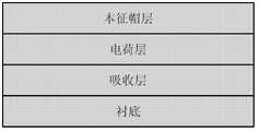
图1示出了现有技术中一种平面型雪崩光电探测器的结构图。如图1所示,该平面型雪崩光电探测器包括:衬底、吸收层、电荷层、本征帽层等。Fig. 1 shows a structure diagram of a planar avalanche photodetector in the prior art. As shown in FIG. 1 , the planar avalanche photodetector includes: a substrate, an absorption layer, a charge layer, an intrinsic cap layer, and the like.
上述现有的技术中,所述本征帽层用于形成中心扩散区和边缘击穿抑制结构,中心扩散区下面的剩余本征帽层部分是器件的倍增层,用于当光生载流子进入倍增层后,在倍增层高电场的作用下与倍增层材料发生碰撞电离,产生更多的自由载流子,从而放大信号。由于曲率效应的存在,器件边缘处往往有高于器件中心处的电场,导致边缘提前击穿,降低器件性能,边缘击穿抑制结构则用于降低器件边缘处的电场,防止器件边缘提前击穿。In the above-mentioned prior art, the intrinsic capping layer is used to form the central diffusion region and the edge breakdown suppression structure, and the remaining intrinsic capping layer part below the central diffusion region is the multiplication layer of the device, which is used to act as a photogenerated carrier After entering the multiplication layer, impact ionization occurs with the multiplication layer material under the action of the high electric field of the multiplication layer, generating more free carriers, thereby amplifying the signal. Due to the existence of the curvature effect, the electric field at the edge of the device is often higher than that at the center of the device, resulting in early breakdown at the edge and reducing the performance of the device. The edge breakdown suppression structure is used to reduce the electric field at the edge of the device and prevent early breakdown at the edge of the device. .
如果能够设计一种结构,既能保持平面型器件高可靠性、低暗电流或暗记数的特性,同时能使倍增区通过材料生长设备精确控制,摆脱扩散或离子注入对器件倍增区厚度的影响,并且将高电场限制在倍增区而使扩散或离子注入区域电场相对较低从而有利于边缘击穿的抑制,使边缘击穿抑制结构有更大的容差,则必将有效提高器件性能。If a structure can be designed, it can not only maintain the characteristics of high reliability, low dark current or dark number of planar devices, but also enable the multiplication region to be precisely controlled by material growth equipment, and get rid of the influence of diffusion or ion implantation on the thickness of the multiplication region of the device , and the high electric field is limited to the multiplication region, and the electric field in the diffusion or ion implantation region is relatively low, which is conducive to the suppression of edge breakdown, and the edge breakdown suppression structure has a greater tolerance, which will effectively improve device performance.
发明内容Contents of the invention
(一)要解决的技术问题(1) Technical problems to be solved
本发明所要解决的技术问题是保持平面型器件高可靠性、低暗电流或暗记数的特性的同时能使倍增区通过材料生长设备精确控制,摆脱扩散或离子注入对器件倍增区厚度的影响,并且将高电场限制在倍增区而使扩散或离子注入区域电场相对较低从而有利于边缘击穿的抑制。The technical problem to be solved by the present invention is to maintain the characteristics of high reliability, low dark current or dark number of planar devices, and at the same time enable the multiplication region to be precisely controlled by material growth equipment, and get rid of the influence of diffusion or ion implantation on the thickness of the multiplication region of the device. And the high electric field is limited in the multiplication region, and the electric field in the diffusion or ion implantation region is relatively low, which is beneficial to the suppression of edge breakdown.
(二)技术方案(2) Technical solution
本发明公开了一种平面型雪崩光电探测器,其外延结构包括:The invention discloses a planar avalanche photodetector, the epitaxial structure of which comprises:
吸收层,其用于吸收目标探测光,将目标探测光的光子转化为光生载流子;The absorbing layer is used to absorb the target detection light, and convert the photons of the target detection light into photogenerated carriers;
N型下电荷层,其用于调控所述雪崩光电探测器器件内部电场分布;N-type lower charge layer, which is used to regulate the internal electric field distribution of the avalanche photodetector device;
倍增层,其用于倍增所述光生载流子;a multiplication layer for multiplying the photogenerated carriers;
P型上电荷层,其也用于调控所述雪崩光电探测器器件内部电场分布;P-type upper charge layer, which is also used to regulate the internal electric field distribution of the avalanche photodetector device;
本征帽层,其用于形成P型中心扩散区和边缘击穿抑制结构;an intrinsic capping layer for forming a P-type central diffusion region and an edge breakdown suppression structure;
其中,所述P型中心扩散区用于形成器件有源区,所述边缘击穿抑制结构用于降低器件边缘处的电场,防止器件边缘提前击穿。Wherein, the P-type central diffusion region is used to form the active region of the device, and the edge breakdown suppression structure is used to reduce the electric field at the edge of the device to prevent early breakdown of the edge of the device.
本发明还公开了一种如上所述的平面型雪崩光电探测器的制备方法,其包括:The present invention also discloses a preparation method of the above-mentioned planar avalanche photodetector, which comprises:
步骤1、生长外延结构,具体包括在N型衬底上,依次生长吸收层、N型下电荷层、倍增层、P型上电荷层和本征帽层;
步骤2、在所述本征帽层上制作P型中心扩散区和边缘击穿抑制结构;
步骤3、在制作有P型中心扩散区和边缘击穿抑制结构的本征帽层上制作P电极;Step 3, making a P electrode on the intrinsic cap layer with a P-type central diffusion region and an edge breakdown suppression structure;
步骤4、在N型衬底背面制作N电极。Step 4, making an N electrode on the back of the N-type substrate.
(三)有益效果(3) Beneficial effects
1、本发明保持平面型雪崩光电探测器高可靠性、低暗电流或暗记数的特性1. The present invention maintains the characteristics of high reliability, low dark current or dark number of planar avalanche photodetectors
2、本发明可以使平面型雪崩光电探测器倍增层厚度通过材料生长设备精确控制,排除了扩散或离子注入对器件倍增层厚度的影响,有利于提高器件的均匀性和可重复行。2. The present invention enables the thickness of the multiplication layer of the planar avalanche photodetector to be precisely controlled by material growth equipment, eliminating the influence of diffusion or ion implantation on the multiplication layer thickness of the device, which is conducive to improving the uniformity and repeatability of the device.
3、本发明将高电场限制在倍增层内,原本高电场的帽层内现在电场相对较低,从而有利于器件边缘击穿的抑制,使边缘击穿抑制结构有更大的容差,器件更容易制备并且对边缘击穿的抑制更加有效。3. In the present invention, the high electric field is limited in the multiplication layer, and the electric field in the cap layer of the original high electric field is relatively low, which is beneficial to the suppression of device edge breakdown, so that the edge breakdown suppression structure has a greater tolerance, and the device Easier to prepare and more effective in suppressing edge breakdown.
附图说明Description of drawings
图1为现有技术中平面型雪崩光电探测器的结构图;Fig. 1 is the structural diagram of planar avalanche photodetector in the prior art;
图2为本发明中平面型雪崩光电探测器的结构图;Fig. 2 is the structural diagram of planar avalanche photodetector in the present invention;
图3为本发明中平面型雪崩光电探测器的制备方法流程图;Fig. 3 is the flow chart of the preparation method of planar avalanche photodetector in the present invention;
图4为本发明制备方法中制作P型中心扩散区和边缘击穿抑制结构步骤3的示意图;4 is a schematic diagram of step 3 of making a P-type central diffusion region and an edge breakdown suppression structure in the preparation method of the present invention;
图5为本发明中平面型雪崩光电探测器的P型电极的示意图形。FIG. 5 is a schematic diagram of a P-type electrode of a planar avalanche photodetector in the present invention.
具体实施方式Detailed ways
为使本发明的目的、技术方案和优点更加清楚明白,以下结合具体实施例,并参照附图,对本发明作进一步的详细说明。In order to make the object, technical solution and advantages of the present invention clearer, the present invention will be further described in detail below in conjunction with specific embodiments and with reference to the accompanying drawings.
图2为本发明提出的平面型雪崩光电探测器(APD)的结构图。所述APD为可以为InGaAs/InP APD。如图2所示,该APD具体从下至上依次包括:FIG. 2 is a structural diagram of a planar avalanche photodetector (APD) proposed by the present invention. The APD may be an InGaAs/InP APD. As shown in Figure 2, the APD specifically includes from bottom to top:
N型衬底,其可以为InP、Si等材料;N-type substrate, which can be InP, Si and other materials;
N型缓冲层,其生长在所述N型衬底上,厚度优选为1um;N-type buffer layer, which is grown on the N-type substrate, preferably with a thickness of 1um;
本征吸收层,其生长在所述N型缓冲层上,其用于吸收目标探测光,将目标探测光的光子转化为光生自由载流子,从而将光信号转化为电信号。其材料由APD的目标探测波长决定,其禁带宽度满足小于目标探测光的光子能量的条件。例如,对于1550nm的目标探测光来说,其可以由In0.53Ga0.47As(GaInAs)、Ge等材料构成,当衬底是InP时,优选为In0.53Ga0.47As,当衬底是Si时,优选为Ge;该吸收层厚度可以为0.1nm到10um,优选为0.1到3um、2um;The intrinsic absorption layer is grown on the N-type buffer layer, and is used for absorbing target detection light, converting photons of the target detection light into photogenerated free carriers, thereby converting optical signals into electrical signals. Its material is determined by the target detection wavelength of the APD, and its forbidden band width satisfies the condition that it is smaller than the photon energy of the target detection light. For example, for the 1550nm target probe light, it can be made of In0.53 Ga0.47 As (GaInAs), Ge and other materials, when the substrate is InP, it is preferably In0.53 Ga0.47 As, when the substrate is Si, Ge is preferred; the thickness of the absorbing layer can be 0.1nm to 10um, preferably 0.1 to 3um, 2um;
N型下电荷层,其用于调控器件内部电场分布,使本征倍增层内有足够高的电场,从而可以发生雪崩倍增,同时使吸收层有适当的电场强度,在保证载流子高速漂移的同时防止吸收层内电场过高,以防止过高的电场产生过大的隧道暗电流或产生有害的雪崩倍增;其材料由APD的目标探测波长决定,其禁带宽度满足小于目标探测光的光子能量的条件。例如,对于1550nm的目标探测光来说,其可以由InP、InAlAs等材料构成,优选为InP,该N型下电荷层层厚度可以为0.1nm到10um,优选为0.05到0.5um、0.26um,且其掺杂浓度优选为1e17/cm3;N-type lower charge layer, which is used to regulate the internal electric field distribution of the device, so that there is a sufficiently high electric field in the intrinsic multiplication layer, so that avalanche multiplication can occur, and at the same time, the absorption layer has an appropriate electric field strength to ensure high-speed carrier drift. At the same time, prevent the electric field in the absorbing layer from being too high, so as to prevent the excessive electric field from generating excessive tunnel dark current or harmful avalanche multiplication; its material is determined by the target detection wavelength of the APD, and its forbidden band width is less than the target detection light. Conditions for photon energy. For example, for the 1550nm target probe light, it can be made of InP, InAlAs and other materials, preferably InP, and the thickness of the N-type lower charge layer can be 0.1nm to 10um, preferably 0.05 to 0.5um, 0.26um, And its doping concentration is preferably 1e17/cm3 ;
本征倍增层,其用于当光生载流子进入本征倍增层后,在本征倍增层高电场的作用下与本征倍增层材料发生碰撞电离,产生更多的自由载流子,从而放大信号。其材料由APD的目标探测波长决定,其禁带宽度满足大于目标探测光的光子能量的条件。例如,对于1550nm的目标探测光来说,其可以由InP等材料或异质结构材料组成,其厚度优选为1um;Intrinsic multiplication layer, which is used for impact ionization with the intrinsic multiplication layer material under the action of the high electric field of the intrinsic multiplication layer after the photogenerated carriers enter the intrinsic multiplication layer to generate more free carriers, thereby Amplify the signal. Its material is determined by the target detection wavelength of the APD, and its forbidden band width satisfies the condition of being greater than the photon energy of the target detection light. For example, for the target probe light of 1550nm, it can be composed of materials such as InP or heterostructure materials, and its thickness is preferably 1um;
P型上电荷层,用于调控器件内部电场分布,使所述本征倍增层内有足够高的电场,从而可以发生雪崩倍增,同时使所述本征倍增层以上本征帽层内P型中心扩散区以及边缘击穿抑制结构以下的部分有适当的电场强度,在保证载流子高速漂移的同时防止其内电场过高,以防止过高的电场产生雪崩倍增或导致边缘击穿。其材料由APD的目标探测波长决定,其禁带宽度满足大于目标探测光的光子能量的条件。例如,对于1550nm的目标探测光来说,其可以由InP、InAlAs等材料构成,优选为InP,该电荷层厚度可以为0.01到10微米,优选为0.05-0.5微米、0.26um,其掺杂浓度优选为1e17/cm3;The P-type upper charge layer is used to regulate the internal electric field distribution of the device, so that there is a sufficiently high electric field in the intrinsic multiplication layer, so that avalanche multiplication can occur, and at the same time make the P-type in the intrinsic cap layer above the intrinsic multiplication layer The central diffusion region and the part below the edge breakdown suppression structure have appropriate electric field strength to ensure high-speed drift of carriers while preventing the internal electric field from being too high, so as to prevent excessive electric field from generating avalanche multiplication or causing edge breakdown. Its material is determined by the target detection wavelength of the APD, and its forbidden band width satisfies the condition of being greater than the photon energy of the target detection light. For example, for the 1550nm target probe light, it can be made of InP, InAlAs and other materials, preferably InP, the thickness of the charge layer can be 0.01 to 10 microns, preferably 0.05-0.5 microns, 0.26um, and its doping concentration Preferably 1e17/cm3 ;
本征帽层,其上用于形成P型中心扩散区和边缘击穿抑制结构,P型中心扩散区下面的剩余本征帽层部分并非器件的倍增区,其作用是分隔P型中心扩散区和P型上电荷层,并使载流子通过此区域进入P型中心扩散区而被P电极收集。The intrinsic cap layer is used to form the P-type central diffusion region and the edge breakdown suppression structure. The remaining intrinsic cap layer under the P-type central diffusion region is not the multiplication region of the device, and its function is to separate the P-type central diffusion region. And the P-type upper charge layer, and the carriers pass through this region into the P-type central diffusion region and are collected by the P electrode.
所述边缘击穿抑制结构用于降低器件边缘处的电场,防止器件边缘提前击穿所述本征帽层,其厚度优选为3.5um,其中,所述P型中心扩散区和边缘击穿抑制结构通过光刻、RIE刻蚀、Zn扩散等工艺形成。The edge breakdown suppression structure is used to reduce the electric field at the edge of the device and prevent the edge of the device from breaking down the intrinsic cap layer in advance, and its thickness is preferably 3.5um, wherein the P-type central diffusion region and the edge breakdown suppression The structure is formed by photolithography, RIE etching, Zn diffusion and other processes.
其中,P电极制作在所述本征帽层上,其通过生长SiO2进行钝化,然后通过生长Au/Zn、Ti/Au形成。N电极制作在所述N型InP衬底背面,其通过生长AuGeNi而形成。Wherein, the P electrode is fabricated on the intrinsic cap layer, which is passivated by growing SiO2 , and then formed by growing Au/Zn, Ti/Au. The N electrode is fabricated on the back of the N-type InP substrate, which is formed by growing AuGeNi.
与现有技术相比,现有技术中所述本征帽层用于形成P型中心扩散区和边缘击穿抑制结构,P型中心扩散区下面的剩余本征帽层部分是器件的倍增层,用于当光生载流子进入倍增层后,在倍增层高电场的作用下与倍增层材料发生碰撞电离,产生更多的自由载流子,从而放大信号。由于曲率效应的存在,器件边缘处往往有高于器件中心处的电场,导致边缘提前击穿,降低器件性能,边缘击穿抑制结构则用于降低器件边缘处的电场,防止器件边缘提前击穿。Compared with the prior art, the intrinsic cap layer in the prior art is used to form the P-type central diffusion region and the edge breakdown suppression structure, and the remaining intrinsic cap layer part under the P-type central diffusion region is the multiplication layer of the device , used for when the photogenerated carriers enter the multiplication layer, under the action of the high electric field of the multiplication layer, impact ionization occurs with the multiplication layer material to generate more free carriers, thereby amplifying the signal. Due to the existence of the curvature effect, the electric field at the edge of the device is often higher than that at the center of the device, resulting in early breakdown at the edge and reducing the performance of the device. The edge breakdown suppression structure is used to reduce the electric field at the edge of the device and prevent early breakdown at the edge of the device. .
而在本发明中,所述本征帽层同样用于形成P型中心扩散区和边缘击穿抑制结构,P型中心扩散区下面的剩余本征帽层部分并非器件的倍增区,其作用是分隔P型中心扩散区和P型上电荷层,并使载流子通过此区域进入P型中心扩散区而被收集。所述边缘击穿抑制结构同样用于降低器件边缘处的电场,防止器件边缘提前击穿。In the present invention, the intrinsic cap layer is also used to form the P-type central diffusion region and the edge breakdown suppression structure, and the remaining intrinsic cap layer part below the P-type central diffusion region is not the multiplication region of the device, and its function is Separate the P-type central diffusion region and the P-type upper charge layer, and allow carriers to enter the P-type central diffusion region through this region to be collected. The edge breakdown suppression structure is also used to reduce the electric field at the edge of the device, preventing premature breakdown of the edge of the device.
图3示出了本发明提出的平面型雪崩光电探测器的一种制备方法。如图3所示,该制备方法包括:Fig. 3 shows a preparation method of the planar avalanche photodetector proposed by the present invention. As shown in Figure 3, the preparation method comprises:
步骤1、外延生长;即在N型衬底上,依次生长吸收层、N型下电荷层、倍增层、P型上电荷层和本征帽层等器件外延层;
步骤2、刻蚀圆坑;在所述本征帽层表面生长SiO2作为掩膜层,利用普通光刻在SiO2掩膜层上开圆孔,通过干法刻蚀在本征帽层上刻蚀圆坑,其深度优选为是0.3-0.5微米,去除SiO2掩膜层;该步骤中还可以通过腐蚀制作圆坑;
步骤3、制作P型中心扩散区和边缘击穿抑制结构;如图4所示,重新在刻蚀有圆坑2的本征帽层1表面生长SiO2作为掩膜层5,利用普通光刻在掩膜层上开圆孔4,同时开圆环3,所述圆孔4与圆环3与步骤2中所述圆坑圆心重合,所述圆孔4的半径大于所述圆坑2的半径,所述圆环3的内径大于所述圆孔4的半径;使用锌扩散或离子注入的方式从所述圆坑2、圆环3和圆孔4将锌扩散至本征帽层1,同时在本征帽层1形成P型中心扩散区和边缘击穿抑制结构;最后去除SiO2。其中,圆孔4与圆环3的圆心与圆坑2的圆心重合。圆坑2以内的Zn扩散区域即为P型中心扩散区,圆坑底部的器件部分即为器件有源区。圆环3下面的Zn扩散区域形成浮动扩散保护环。通过刻蚀圆坑,P型中心扩散区即圆坑2所在区域与其边缘部分即圆孔4比圆坑2大的区域形成一个台阶,这个台阶和浮动扩散保护环共同构成器件的边缘击穿抑制结构,可以有效降低器件边缘电场,防止器件边缘击穿,提高器件性能。Step 3, making a P-type central diffusion region and an edge breakdown suppression structure; as shown in Figure 4, re-grow SiO2 on the surface of the
步骤4、钝化、开口;重新生长SiO2作为钝化层,利用普通光刻在其上开圆孔,此圆孔与步骤2中刻蚀的圆坑圆心重叠,且所述圆孔的半径大于所述圆坑的半径。Step 4, passivation, opening; re-grow SiO2 as a passivation layer, and use ordinary photolithography to open a round hole on it. This round hole overlaps with the center of the round pit etched in
步骤5、生长Au/Zn;在步骤4形成的圆孔上,利用普通光刻、剥离技术生长Au/Zn金属环,金属环圆心与步骤1中所述圆坑圆心重叠,所述金属环的外径可大于或等于步骤4中形成的圆孔,以将所述圆孔边缘覆盖。
步骤6、生长Ti/Au;利用普通光刻、剥离技术生长Ti/Au作为P电极。P电极由金属环、圆形金属垫和连接两者的金属条组成,其中金属环覆盖在步骤5所述Au/Zn金属环上,其圆心与步骤2中所述圆坑圆心重叠,其形状如图5所示,所述金属垫和金属条制作在所述钝化层上。Step 6, growing Ti/Au; using ordinary photolithography and lift-off techniques to grow Ti/Au as a P electrode. The P electrode consists of a metal ring, a circular metal pad and a metal strip connecting the two, wherein the metal ring is covered on the Au/Zn metal ring described in
步骤7、生长AuGeNi:在外延片衬底背面上溅射300nm厚的AuGeNi作为N电极。Step 7, growing AuGeNi: AuGeNi with a thickness of 300 nm is sputtered on the back surface of the epitaxial wafer substrate as an N electrode.
以上所述的具体实施例,对本发明的目的、技术方案和有益效果进行了进一步详细说明,应理解的是,以上所述仅为本发明的具体实施例而已,并不用于限制本发明,凡在本发明的精神和原则之内,所做的任何修改、等同替换、改进等,均应包含在本发明的保护范围之内。The specific embodiments described above have further described the purpose, technical solutions and beneficial effects of the present invention in detail. It should be understood that the above descriptions are only specific embodiments of the present invention, and are not intended to limit the present invention. Within the spirit and principles of the present invention, any modifications, equivalent replacements, improvements, etc., shall be included in the protection scope of the present invention.
Claims (11)
Translated fromChinesePriority Applications (1)
| Application Number | Priority Date | Filing Date | Title |
|---|---|---|---|
| CN201310136829XACN103227231A (en) | 2013-04-19 | 2013-04-19 | Planar avalanche photoelectric detector |
Applications Claiming Priority (1)
| Application Number | Priority Date | Filing Date | Title |
|---|---|---|---|
| CN201310136829XACN103227231A (en) | 2013-04-19 | 2013-04-19 | Planar avalanche photoelectric detector |
Publications (1)
| Publication Number | Publication Date |
|---|---|
| CN103227231Atrue CN103227231A (en) | 2013-07-31 |
Family
ID=48837601
Family Applications (1)
| Application Number | Title | Priority Date | Filing Date |
|---|---|---|---|
| CN201310136829XAPendingCN103227231A (en) | 2013-04-19 | 2013-04-19 | Planar avalanche photoelectric detector |
Country Status (1)
| Country | Link |
|---|---|
| CN (1) | CN103227231A (en) |
Cited By (7)
| Publication number | Priority date | Publication date | Assignee | Title |
|---|---|---|---|---|
| CN105789366A (en)* | 2016-03-16 | 2016-07-20 | 中国科学院半导体研究所 | Silicon-based hybrid integrated avalanche photodetector |
| CN107003180A (en)* | 2014-10-21 | 2017-08-01 | 库卡工业有限两合公司 | Method for monitoring radiation |
| CN107092760A (en)* | 2017-05-05 | 2017-08-25 | 中国科学院半导体研究所 | The method of adjustment of avalanche photodide device and its structural parameters |
| WO2020124205A1 (en)* | 2018-12-19 | 2020-06-25 | National Research Council Of Canada | Method of fabricating an avalanche photodiode employing single diffusion |
| CN111510124A (en)* | 2020-03-20 | 2020-08-07 | 中国工程物理研究院流体物理研究所 | Magnetic bias weak light triggering high-power photoconductive switch |
| WO2022061831A1 (en)* | 2020-09-27 | 2022-03-31 | 深圳市大疆创新科技有限公司 | Diode and manufacturing method therefor, receiving chip, distance measurement device, and movable platform |
| CN116171393A (en)* | 2020-11-30 | 2023-05-26 | 苏州帧观传感科技有限公司 | Image sensor based on charge carrier avalanche |
Citations (3)
| Publication number | Priority date | Publication date | Assignee | Title |
|---|---|---|---|---|
| EP2175497A2 (en)* | 2008-08-12 | 2010-04-14 | Acreo AB | A photodiode |
| CN102257641A (en)* | 2008-12-18 | 2011-11-23 | 阿尔卡特朗讯 | Avalanche photodiode |
| CN102412343A (en)* | 2011-11-30 | 2012-04-11 | 中国科学院半导体研究所 | Fabrication method of planar avalanche diode detector applicable to single photon detection |
- 2013
- 2013-04-19CNCN201310136829XApatent/CN103227231A/enactivePending
Patent Citations (3)
| Publication number | Priority date | Publication date | Assignee | Title |
|---|---|---|---|---|
| EP2175497A2 (en)* | 2008-08-12 | 2010-04-14 | Acreo AB | A photodiode |
| CN102257641A (en)* | 2008-12-18 | 2011-11-23 | 阿尔卡特朗讯 | Avalanche photodiode |
| CN102412343A (en)* | 2011-11-30 | 2012-04-11 | 中国科学院半导体研究所 | Fabrication method of planar avalanche diode detector applicable to single photon detection |
Cited By (11)
| Publication number | Priority date | Publication date | Assignee | Title |
|---|---|---|---|---|
| CN107003180A (en)* | 2014-10-21 | 2017-08-01 | 库卡工业有限两合公司 | Method for monitoring radiation |
| US10247601B2 (en) | 2014-10-21 | 2019-04-02 | Kuka Detuschland Gmbh | Method for monitoring radiation |
| CN105789366A (en)* | 2016-03-16 | 2016-07-20 | 中国科学院半导体研究所 | Silicon-based hybrid integrated avalanche photodetector |
| CN105789366B (en)* | 2016-03-16 | 2017-07-28 | 中国科学院半导体研究所 | A kind of silicon substrate hybrid integrated avalanche photodetector |
| CN107092760A (en)* | 2017-05-05 | 2017-08-25 | 中国科学院半导体研究所 | The method of adjustment of avalanche photodide device and its structural parameters |
| WO2020124205A1 (en)* | 2018-12-19 | 2020-06-25 | National Research Council Of Canada | Method of fabricating an avalanche photodiode employing single diffusion |
| US11837681B2 (en) | 2018-12-19 | 2023-12-05 | National Research Council Of Canada | Method of fabricating an avalanche photodiode employing single diffusion |
| CN111510124A (en)* | 2020-03-20 | 2020-08-07 | 中国工程物理研究院流体物理研究所 | Magnetic bias weak light triggering high-power photoconductive switch |
| CN111510124B (en)* | 2020-03-20 | 2023-03-24 | 中国工程物理研究院流体物理研究所 | Magnetic bias weak light triggering high-power photoconductive switch |
| WO2022061831A1 (en)* | 2020-09-27 | 2022-03-31 | 深圳市大疆创新科技有限公司 | Diode and manufacturing method therefor, receiving chip, distance measurement device, and movable platform |
| CN116171393A (en)* | 2020-11-30 | 2023-05-26 | 苏州帧观传感科技有限公司 | Image sensor based on charge carrier avalanche |
Similar Documents
| Publication | Publication Date | Title |
|---|---|---|
| CN103227231A (en) | Planar avalanche photoelectric detector | |
| CN105405916B (en) | Silicon-based wide spectrum detector and preparation method therefor | |
| CN102290481B (en) | Silicon detector structure with broad spectral response and method of making same | |
| CN103400872B (en) | Structure of the PIN photoelectric detector that surface field strengthens and preparation method thereof | |
| CN104465853B (en) | Avalanche photodiode and manufacturing method thereof | |
| CN100438083C (en) | Ultraviolet photoelectric detector delta doped 4H-SiC PIN structure | |
| CN105304748B (en) | 4H SiC UV photodetectors of double working modes and preparation method thereof | |
| CN102412343B (en) | Manufacturing method of flat-type avalanche diode detector used for detecting single photon | |
| CN113921646B (en) | Single-photon detector, manufacturing method thereof and single-photon detector array | |
| CN106299016B (en) | A kind of avalanche photodide and preparation method thereof | |
| JP6024755B2 (en) | Semiconductor light receiving element and manufacturing method thereof | |
| CN113707751B (en) | Single photon avalanche photoelectric detector and preparation method thereof | |
| CN106847960A (en) | A kind of single-photon avalanche diode and its manufacture craft based on deep N-well structure | |
| CN105405917A (en) | Mesa type avalanche photoelectric detector | |
| CN109346552B (en) | Avalanche photodetector based on arc diffusion region and manufacturing method thereof | |
| CN108231919A (en) | A kind of silicon carbide avalanche photodetector with graphene transparent electrode | |
| CN110311000A (en) | Two-type superlattice avalanche photodetector and manufacturing method thereof | |
| CN108807567A (en) | A kind of mercury cadmium telluride avalanche diode detector of modulated surface energy band | |
| CN105097964B (en) | A Gaussian-doped pπn ultraviolet detector with active region | |
| CN110350045A (en) | PbS quantum Si-APD infrared detector and preparation method thereof | |
| KR20150012303A (en) | Planar avalanche photodiode | |
| CN105185845A (en) | Si-PIN photodetector introducing micro-structure silicon in P layer and N layer and preparation method thereof | |
| CN108400196A (en) | One kind having superlattice structure gallium nitride base ultraviolet light electric explorer and preparation method thereof | |
| CN104617181B (en) | ITO current expansion layer based InGaAs avalanche infrared detector and preparation method thereof | |
| CN113964238B (en) | A kind of preparation method of avalanche photoelectric detector |
Legal Events
| Date | Code | Title | Description |
|---|---|---|---|
| C06 | Publication | ||
| PB01 | Publication | ||
| C10 | Entry into substantive examination | ||
| SE01 | Entry into force of request for substantive examination | ||
| C02 | Deemed withdrawal of patent application after publication (patent law 2001) | ||
| WD01 | Invention patent application deemed withdrawn after publication | Application publication date:20130731 |