CN103225071A - Method for depositing a chlorine-free conformal SiN film - Google Patents
Method for depositing a chlorine-free conformal SiN filmDownload PDFInfo
- Publication number
- CN103225071A CN103225071ACN2013100214608ACN201310021460ACN103225071ACN 103225071 ACN103225071 ACN 103225071ACN 2013100214608 ACN2013100214608 ACN 2013100214608ACN 201310021460 ACN201310021460 ACN 201310021460ACN 103225071 ACN103225071 ACN 103225071A
- Authority
- CN
- China
- Prior art keywords
- reactant
- substrate
- plasma
- nitrogen
- carbon
- Prior art date
- Legal status (The legal status is an assumption and is not a legal conclusion. Google has not performed a legal analysis and makes no representation as to the accuracy of the status listed.)
- Pending
Links
- 238000000034methodMethods0.000titleclaimsabstractdescription135
- 238000000151depositionMethods0.000titleabstractdescription48
- 229910052581Si3N4Inorganic materials0.000claimsabstractdescription123
- HQVNEWCFYHHQES-UHFFFAOYSA-Nsilicon nitrideChemical compoundN12[Si]34N5[Si]62N3[Si]51N64HQVNEWCFYHHQES-UHFFFAOYSA-N0.000claimsabstractdescription123
- 239000000758substrateSubstances0.000claimsabstractdescription116
- 239000000463materialSubstances0.000claimsabstractdescription19
- 239000000376reactantSubstances0.000claimsdescription256
- QJGQUHMNIGDVPM-UHFFFAOYSA-Nnitrogen groupChemical group[N]QJGQUHMNIGDVPM-UHFFFAOYSA-N0.000claimsdescription83
- 239000012071phaseSubstances0.000claimsdescription63
- 239000007789gasSubstances0.000claimsdescription51
- IJGRMHOSHXDMSA-UHFFFAOYSA-NAtomic nitrogenChemical compoundN#NIJGRMHOSHXDMSA-UHFFFAOYSA-N0.000claimsdescription46
- 238000006243chemical reactionMethods0.000claimsdescription40
- 230000008021depositionEffects0.000claimsdescription36
- 229910052799carbonInorganic materials0.000claimsdescription35
- OKTJSMMVPCPJKN-UHFFFAOYSA-NCarbonChemical compound[C]OKTJSMMVPCPJKN-UHFFFAOYSA-N0.000claimsdescription33
- 229910052757nitrogenInorganic materials0.000claimsdescription26
- 150000003973alkyl aminesChemical class0.000claimsdescription14
- 229910052736halogenInorganic materials0.000claimsdescription10
- 150000002367halogensChemical class0.000claimsdescription10
- 230000004913activationEffects0.000claimsdescription7
- 150000001412aminesChemical class0.000claimsdescription6
- 239000003153chemical reaction reagentSubstances0.000claimsdescription6
- 239000012808vapor phaseSubstances0.000claimsdescription5
- 230000015572biosynthetic processEffects0.000claimsdescription4
- DTFIGXKKZTXXQS-UHFFFAOYSA-NN#[Si][SiH2][SiH3]Chemical compoundN#[Si][SiH2][SiH3]DTFIGXKKZTXXQS-UHFFFAOYSA-N0.000claims1
- 229910001245Sb alloyInorganic materials0.000claims1
- 239000002140antimony alloySubstances0.000claims1
- VOSJXMPCFODQAR-UHFFFAOYSA-Nac1l3fa4Chemical compound[SiH3]N([SiH3])[SiH3]VOSJXMPCFODQAR-UHFFFAOYSA-N0.000abstractdescription61
- XUIMIQQOPSSXEZ-UHFFFAOYSA-NSiliconChemical compound[Si]XUIMIQQOPSSXEZ-UHFFFAOYSA-N0.000abstractdescription38
- 229910052710siliconInorganic materials0.000abstractdescription38
- 239000010703siliconSubstances0.000abstractdescription37
- 239000002243precursorSubstances0.000abstractdescription3
- 239000010408filmSubstances0.000description136
- 210000002381plasmaAnatomy0.000description90
- QGZKDVFQNNGYKY-UHFFFAOYSA-NAmmoniaChemical compoundNQGZKDVFQNNGYKY-UHFFFAOYSA-N0.000description73
- 238000012545processingMethods0.000description48
- 230000008569processEffects0.000description45
- 229910021529ammoniaInorganic materials0.000description36
- YBRBMKDOPFTVDT-UHFFFAOYSA-Ntert-butylamineChemical groupCC(C)(C)NYBRBMKDOPFTVDT-UHFFFAOYSA-N0.000description31
- 235000012431wafersNutrition0.000description26
- 239000011261inert gasSubstances0.000description18
- 239000007788liquidSubstances0.000description17
- OAKJQQAXSVQMHS-UHFFFAOYSA-NHydrazineChemical compoundNNOAKJQQAXSVQMHS-UHFFFAOYSA-N0.000description16
- 238000010926purgeMethods0.000description16
- VQTUBCCKSQIDNK-UHFFFAOYSA-NIsobuteneChemical compoundCC(C)=CVQTUBCCKSQIDNK-UHFFFAOYSA-N0.000description15
- 238000000231atomic layer depositionMethods0.000description14
- NJPPVKZQTLUDBO-UHFFFAOYSA-NnovaluronChemical compoundC1=C(Cl)C(OC(F)(F)C(OC(F)(F)F)F)=CC=C1NC(=O)NC(=O)C1=C(F)C=CC=C1FNJPPVKZQTLUDBO-UHFFFAOYSA-N0.000description14
- 229910052739hydrogenInorganic materials0.000description13
- 238000011282treatmentMethods0.000description13
- 239000000203mixtureSubstances0.000description11
- 238000000678plasma activationMethods0.000description11
- 238000012546transferMethods0.000description11
- 230000008016vaporizationEffects0.000description11
- 238000005229chemical vapour depositionMethods0.000description10
- 238000002156mixingMethods0.000description10
- 238000009834vaporizationMethods0.000description10
- 239000006227byproductSubstances0.000description9
- MROCJMGDEKINLD-UHFFFAOYSA-NdichlorosilaneChemical compoundCl[SiH2]ClMROCJMGDEKINLD-UHFFFAOYSA-N0.000description9
- 239000001257hydrogenSubstances0.000description9
- FZHAPNGMFPVSLP-UHFFFAOYSA-NsilanamineChemical compound[SiH3]NFZHAPNGMFPVSLP-UHFFFAOYSA-N0.000description9
- XKRFYHLGVUSROY-UHFFFAOYSA-NArgonChemical compound[Ar]XKRFYHLGVUSROY-UHFFFAOYSA-N0.000description8
- 238000010438heat treatmentMethods0.000description8
- 230000007246mechanismEffects0.000description8
- RYGMFSIKBFXOCR-UHFFFAOYSA-NCopperChemical compound[Cu]RYGMFSIKBFXOCR-UHFFFAOYSA-N0.000description7
- UFHFLCQGNIYNRP-UHFFFAOYSA-NHydrogenChemical compound[H][H]UFHFLCQGNIYNRP-UHFFFAOYSA-N0.000description7
- 125000000217alkyl groupChemical group0.000description7
- 229910052802copperInorganic materials0.000description7
- 239000010949copperSubstances0.000description7
- 238000001179sorption measurementMethods0.000description7
- CURLTUGMZLYLDI-UHFFFAOYSA-NCarbon dioxideChemical compoundO=C=OCURLTUGMZLYLDI-UHFFFAOYSA-N0.000description6
- CKUAXEQHGKSLHN-UHFFFAOYSA-N[C].[N]Chemical compound[C].[N]CKUAXEQHGKSLHN-UHFFFAOYSA-N0.000description6
- 238000005137deposition processMethods0.000description6
- 239000001307heliumSubstances0.000description6
- 229910052734heliumInorganic materials0.000description6
- SWQJXJOGLNCZEY-UHFFFAOYSA-Nhelium atomChemical compound[He]SWQJXJOGLNCZEY-UHFFFAOYSA-N0.000description6
- 238000004519manufacturing processMethods0.000description6
- 150000003254radicalsChemical class0.000description6
- 239000004065semiconductorSubstances0.000description6
- 238000003860storageMethods0.000description6
- 238000006557surface reactionMethods0.000description6
- 238000010408sweepingMethods0.000description6
- 125000000999tert-butyl groupChemical group[H]C([H])([H])C(*)(C([H])([H])[H])C([H])([H])[H]0.000description6
- 239000010409thin filmSubstances0.000description6
- 229910045601alloyInorganic materials0.000description5
- 239000000956alloySubstances0.000description5
- 238000010574gas phase reactionMethods0.000description5
- 238000009832plasma treatmentMethods0.000description5
- QUSNBJAOOMFDIB-UHFFFAOYSA-NEthylamineChemical compoundCCNQUSNBJAOOMFDIB-UHFFFAOYSA-N0.000description4
- 229910052786argonInorganic materials0.000description4
- 239000012159carrier gasSubstances0.000description4
- KOPOQZFJUQMUML-UHFFFAOYSA-NchlorosilaneChemical compoundCl[SiH3]KOPOQZFJUQMUML-UHFFFAOYSA-N0.000description4
- 230000000694effectsEffects0.000description4
- 238000003379elimination reactionMethods0.000description4
- 238000011065in-situ storageMethods0.000description4
- 229920002120photoresistant polymerPolymers0.000description4
- 125000005931tert-butyloxycarbonyl groupChemical group[H]C([H])([H])C(OC(*)=O)(C([H])([H])[H])C([H])([H])[H]0.000description4
- WFKWXMTUELFFGS-UHFFFAOYSA-NtungstenChemical compound[W]WFKWXMTUELFFGS-UHFFFAOYSA-N0.000description4
- 229910052721tungstenInorganic materials0.000description4
- 239000010937tungstenSubstances0.000description4
- 239000005046ChlorosilaneSubstances0.000description3
- VYPSYNLAJGMNEJ-UHFFFAOYSA-NSilicium dioxideChemical compoundO=[Si]=OVYPSYNLAJGMNEJ-UHFFFAOYSA-N0.000description3
- QVGXLLKOCUKJST-UHFFFAOYSA-Natomic oxygenChemical compound[O]QVGXLLKOCUKJST-UHFFFAOYSA-N0.000description3
- 125000004432carbon atomChemical groupC*0.000description3
- 229910002092carbon dioxideInorganic materials0.000description3
- 239000001569carbon dioxideSubstances0.000description3
- 238000010586diagramMethods0.000description3
- UAOMVDZJSHZZME-UHFFFAOYSA-NdiisopropylamineChemical compoundCC(C)NC(C)CUAOMVDZJSHZZME-UHFFFAOYSA-N0.000description3
- 238000009826distributionMethods0.000description3
- 238000012986modificationMethods0.000description3
- 230000004048modificationEffects0.000description3
- 125000004433nitrogen atomChemical groupN*0.000description3
- 229910052760oxygenInorganic materials0.000description3
- 239000001301oxygenSubstances0.000description3
- 238000000059patterningMethods0.000description3
- 238000000623plasma-assisted chemical vapour depositionMethods0.000description3
- 125000001424substituent groupChemical group0.000description3
- NBKZGRPRTQELKX-UHFFFAOYSA-N(2-methylpropan-2-yl)oxymethanoneChemical compoundCC(C)(C)O[C]=ONBKZGRPRTQELKX-UHFFFAOYSA-N0.000description2
- PAYRUJLWNCNPSJ-UHFFFAOYSA-NAnilineChemical compoundNC1=CC=CC=C1PAYRUJLWNCNPSJ-UHFFFAOYSA-N0.000description2
- VEXZGXHMUGYJMC-UHFFFAOYSA-MChloride anionChemical compound[Cl-]VEXZGXHMUGYJMC-UHFFFAOYSA-M0.000description2
- ROSDSFDQCJNGOL-UHFFFAOYSA-NDimethylamineChemical compoundCNCROSDSFDQCJNGOL-UHFFFAOYSA-N0.000description2
- 229910000618GeSbTeInorganic materials0.000description2
- BAVYZALUXZFZLV-UHFFFAOYSA-NMethylamineChemical compoundNCBAVYZALUXZFZLV-UHFFFAOYSA-N0.000description2
- JUJWROOIHBZHMG-UHFFFAOYSA-NPyridineChemical compoundC1=CC=NC=C1JUJWROOIHBZHMG-UHFFFAOYSA-N0.000description2
- -1S-butylchlorosilaneChemical compound0.000description2
- 229910004298SiO 2Inorganic materials0.000description2
- BLRPTPMANUNPDV-UHFFFAOYSA-NSilaneChemical compound[SiH4]BLRPTPMANUNPDV-UHFFFAOYSA-N0.000description2
- RTAQQCXQSZGOHL-UHFFFAOYSA-NTitaniumChemical compound[Ti]RTAQQCXQSZGOHL-UHFFFAOYSA-N0.000description2
- 238000001994activationMethods0.000description2
- 230000004888barrier functionEffects0.000description2
- WGQKYBSKWIADBV-UHFFFAOYSA-NbenzylamineChemical compoundNCC1=CC=CC=C1WGQKYBSKWIADBV-UHFFFAOYSA-N0.000description2
- 150000001721carbonChemical group0.000description2
- 230000008859changeEffects0.000description2
- 239000000460chlorineSubstances0.000description2
- 238000004140cleaningMethods0.000description2
- 238000004891communicationMethods0.000description2
- 238000011109contaminationMethods0.000description2
- 125000004122cyclic groupChemical group0.000description2
- KZZKOVLJUKWSKX-UHFFFAOYSA-NcyclobutanamineChemical compoundNC1CCC1KZZKOVLJUKWSKX-UHFFFAOYSA-N0.000description2
- 238000000354decomposition reactionMethods0.000description2
- 230000007423decreaseEffects0.000description2
- 238000005530etchingMethods0.000description2
- 150000004820halidesChemical class0.000description2
- BMFVGAAISNGQNM-UHFFFAOYSA-NisopentylamineChemical compoundCC(C)CCNBMFVGAAISNGQNM-UHFFFAOYSA-N0.000description2
- JJWLVOIRVHMVIS-UHFFFAOYSA-NisopropylamineChemical compoundCC(C)NJJWLVOIRVHMVIS-UHFFFAOYSA-N0.000description2
- 239000003446ligandSubstances0.000description2
- 239000012528membraneSubstances0.000description2
- 229910052751metalInorganic materials0.000description2
- 239000002184metalSubstances0.000description2
- XWESXZZECGOXDQ-UHFFFAOYSA-Nn-tert-butylhydroxylamineChemical compoundCC(C)(C)NOXWESXZZECGOXDQ-UHFFFAOYSA-N0.000description2
- 239000002245particleSubstances0.000description2
- 238000009428plumbingMethods0.000description2
- 238000011112process operationMethods0.000description2
- WGYKZJWCGVVSQN-UHFFFAOYSA-NpropylamineChemical compoundCCCNWGYKZJWCGVVSQN-UHFFFAOYSA-N0.000description2
- BHRZNVHARXXAHW-UHFFFAOYSA-Nsec-butylamineChemical compoundCCC(C)NBHRZNVHARXXAHW-UHFFFAOYSA-N0.000description2
- 238000000926separation methodMethods0.000description2
- 229910000077silaneInorganic materials0.000description2
- 150000004756silanesChemical class0.000description2
- 150000003377silicon compoundsChemical class0.000description2
- 125000006850spacer groupChemical group0.000description2
- 230000006641stabilisationEffects0.000description2
- 238000011105stabilizationMethods0.000description2
- 239000000126substanceSubstances0.000description2
- 238000005979thermal decomposition reactionMethods0.000description2
- 229910052719titaniumInorganic materials0.000description2
- 239000010936titaniumSubstances0.000description2
- GETQZCLCWQTVFV-UHFFFAOYSA-NtrimethylamineChemical compoundCN(C)CGETQZCLCWQTVFV-UHFFFAOYSA-N0.000description2
- 238000011144upstream manufacturingMethods0.000description2
- JZKAJIFHBZJCAI-UHFFFAOYSA-N1,2-ditert-butylhydrazineChemical compoundCC(C)(C)NNC(C)(C)CJZKAJIFHBZJCAI-UHFFFAOYSA-N0.000description1
- WNYSBZGPJNISEC-UHFFFAOYSA-N2,3-dimethylbutan-2-amineChemical compoundCC(C)C(C)(C)N.CC(C)C(C)(C)NWNYSBZGPJNISEC-UHFFFAOYSA-N0.000description1
- BEEYLGLWYXWFAG-UHFFFAOYSA-N2-aminosilyl-2-methylpropaneChemical compoundCC(C)(C)[SiH2]NBEEYLGLWYXWFAG-UHFFFAOYSA-N0.000description1
- VUGMARFZKDASCX-UHFFFAOYSA-N2-methyl-N-silylpropan-2-amineChemical compoundCC(C)(C)N[SiH3]VUGMARFZKDASCX-UHFFFAOYSA-N0.000description1
- GELMWIVBBPAMIO-UHFFFAOYSA-N2-methylbutan-2-amineChemical compoundCCC(C)(C)NGELMWIVBBPAMIO-UHFFFAOYSA-N0.000description1
- NLXLAEXVIDQMFP-UHFFFAOYSA-NAmmonia chlorideChemical compound[NH4+].[Cl-]NLXLAEXVIDQMFP-UHFFFAOYSA-N0.000description1
- MXJZBJMDVJSUET-UHFFFAOYSA-NC(C)(C)(CC)N.C(CC(C)C)NChemical compoundC(C)(C)(CC)N.C(CC(C)C)NMXJZBJMDVJSUET-UHFFFAOYSA-N0.000description1
- ZAMOUSCENKQFHK-UHFFFAOYSA-NChlorine atomChemical compound[Cl]ZAMOUSCENKQFHK-UHFFFAOYSA-N0.000description1
- HTJDQJBWANPRPF-UHFFFAOYSA-NCyclopropylamineChemical compoundNC1CC1HTJDQJBWANPRPF-UHFFFAOYSA-N0.000description1
- 238000005033Fourier transform infrared spectroscopyMethods0.000description1
- AVXURJPOCDRRFD-UHFFFAOYSA-NHydroxylamineChemical compoundONAVXURJPOCDRRFD-UHFFFAOYSA-N0.000description1
- 229910003902SiCl 4Inorganic materials0.000description1
- 238000003848UV Light-CuringMethods0.000description1
- UMVBXBACMIOFDO-UHFFFAOYSA-N[N].[Si]Chemical compound[N].[Si]UMVBXBACMIOFDO-UHFFFAOYSA-N0.000description1
- QIQXHTLMLNTEDX-UHFFFAOYSA-N[SiH4].C(C)[SiH2]CCChemical compound[SiH4].C(C)[SiH2]CCQIQXHTLMLNTEDX-UHFFFAOYSA-N0.000description1
- DJWUWYCIBXAGIZ-UHFFFAOYSA-N[SiH4].CC(C)(C)[Si](C)(C)ClChemical compound[SiH4].CC(C)(C)[Si](C)(C)ClDJWUWYCIBXAGIZ-UHFFFAOYSA-N0.000description1
- WWMIQJRAIZFZKA-UHFFFAOYSA-N[Si].N[SiH3]Chemical compound[Si].N[SiH3]WWMIQJRAIZFZKA-UHFFFAOYSA-N0.000description1
- 125000003342alkenyl groupChemical group0.000description1
- 125000000304alkynyl groupChemical group0.000description1
- 229910052782aluminiumInorganic materials0.000description1
- XAGFODPZIPBFFR-UHFFFAOYSA-NaluminiumChemical compound[Al]XAGFODPZIPBFFR-UHFFFAOYSA-N0.000description1
- 235000019270ammonium chlorideNutrition0.000description1
- 238000004458analytical methodMethods0.000description1
- 238000000137annealingMethods0.000description1
- 230000003667anti-reflective effectEffects0.000description1
- 238000013459approachMethods0.000description1
- 150000004982aromatic aminesChemical class0.000description1
- 230000008901benefitEffects0.000description1
- 230000033228biological regulationEffects0.000description1
- VQPFDLRNOCQMSN-UHFFFAOYSA-NbromosilaneChemical classBr[SiH3]VQPFDLRNOCQMSN-UHFFFAOYSA-N0.000description1
- VBLDUBUUQYXSCG-UHFFFAOYSA-Nbutan-2-ylsilaneChemical compoundCCC(C)[SiH3]VBLDUBUUQYXSCG-UHFFFAOYSA-N0.000description1
- 150000001723carbon free-radicalsChemical class0.000description1
- 229910052801chlorineInorganic materials0.000description1
- QABCGOSYZHCPGN-UHFFFAOYSA-Nchloro(dimethyl)siliconChemical compoundC[Si](C)ClQABCGOSYZHCPGN-UHFFFAOYSA-N0.000description1
- VNJCDDZVNHPVNM-UHFFFAOYSA-Nchloro(ethyl)silaneChemical compoundCC[SiH2]ClVNJCDDZVNHPVNM-UHFFFAOYSA-N0.000description1
- YGZSVWMBUCGDCV-UHFFFAOYSA-Nchloro(methyl)silaneChemical compoundC[SiH2]ClYGZSVWMBUCGDCV-UHFFFAOYSA-N0.000description1
- CRIVIYPBVUGWSC-UHFFFAOYSA-Nchloro(propan-2-yl)silaneChemical compoundCC(C)[SiH2]ClCRIVIYPBVUGWSC-UHFFFAOYSA-N0.000description1
- BGPCFXZWLWDDDU-UHFFFAOYSA-Nchloro(propyl)silaneChemical compoundCCC[SiH2]ClBGPCFXZWLWDDDU-UHFFFAOYSA-N0.000description1
- KAADXUXXXANQKW-UHFFFAOYSA-Nchloro-dimethyl-(2-methylpentan-2-yl)silaneChemical compoundCCCC(C)(C)[Si](C)(C)ClKAADXUXXXANQKW-UHFFFAOYSA-N0.000description1
- SLLGVCUQYRMELA-UHFFFAOYSA-NchlorosiliconChemical compoundCl[Si]SLLGVCUQYRMELA-UHFFFAOYSA-N0.000description1
- 238000003776cleavage reactionMethods0.000description1
- 150000001875compoundsChemical class0.000description1
- 230000003750conditioning effectEffects0.000description1
- 238000005260corrosionMethods0.000description1
- 230000007797corrosionEffects0.000description1
- 230000008878couplingEffects0.000description1
- 238000010168coupling processMethods0.000description1
- 238000005859coupling reactionMethods0.000description1
- 150000001924cycloalkanesChemical class0.000description1
- 125000000753cycloalkyl groupChemical group0.000description1
- 230000002950deficientEffects0.000description1
- 230000001934delayEffects0.000description1
- 238000003795desorptionMethods0.000description1
- KTQYJQFGNYHXMB-UHFFFAOYSA-Ndichloro(methyl)siliconChemical compoundC[Si](Cl)ClKTQYJQFGNYHXMB-UHFFFAOYSA-N0.000description1
- 239000003989dielectric materialSubstances0.000description1
- 238000009792diffusion processMethods0.000description1
- 229940043279diisopropylamineDrugs0.000description1
- UBHZUDXTHNMNLD-UHFFFAOYSA-NdimethylsilaneChemical compoundC[SiH2]CUBHZUDXTHNMNLD-UHFFFAOYSA-N0.000description1
- PZPGRFITIJYNEJ-UHFFFAOYSA-NdisilaneChemical compound[SiH3][SiH3]PZPGRFITIJYNEJ-UHFFFAOYSA-N0.000description1
- PRWJWJFNTJLFKK-UHFFFAOYSA-Nditert-butyl(chloro)siliconChemical compoundCC(C)(C)[Si](Cl)C(C)(C)CPRWJWJFNTJLFKK-UHFFFAOYSA-N0.000description1
- LFLMSLJSSVNEJH-UHFFFAOYSA-Nditert-butyl(silyl)silaneChemical compoundCC(C)(C)[SiH]([SiH3])C(C)(C)CLFLMSLJSSVNEJH-UHFFFAOYSA-N0.000description1
- JTGAUXSVQKWNHO-UHFFFAOYSA-Nditert-butylsiliconChemical compoundCC(C)(C)[Si]C(C)(C)CJTGAUXSVQKWNHO-UHFFFAOYSA-N0.000description1
- 230000005684electric fieldEffects0.000description1
- 230000005670electromagnetic radiationEffects0.000description1
- 230000008030eliminationEffects0.000description1
- 238000005538encapsulationMethods0.000description1
- 125000001495ethyl groupChemical group[H]C([H])([H])C([H])([H])*0.000description1
- KCWYOFZQRFCIIE-UHFFFAOYSA-NethylsilaneChemical compoundCC[SiH3]KCWYOFZQRFCIIE-UHFFFAOYSA-N0.000description1
- 239000012530fluidSubstances0.000description1
- 239000003574free electronSubstances0.000description1
- 125000005843halogen groupChemical group0.000description1
- 125000005842heteroatomChemical group0.000description1
- QGGUMTNPIYCTSF-UHFFFAOYSA-NhexylsilaneChemical compoundCCCCCC[SiH3]QGGUMTNPIYCTSF-UHFFFAOYSA-N0.000description1
- 150000002431hydrogenChemical class0.000description1
- 125000004435hydrogen atomChemical group[H]*0.000description1
- 238000009616inductively coupled plasmaMethods0.000description1
- 238000009413insulationMethods0.000description1
- 230000010354integrationEffects0.000description1
- IDIOJRGTRFRIJL-UHFFFAOYSA-NiodosilaneChemical classI[SiH3]IDIOJRGTRFRIJL-UHFFFAOYSA-N0.000description1
- 238000010849ion bombardmentMethods0.000description1
- 238000005468ion implantationMethods0.000description1
- 238000001459lithographyMethods0.000description1
- 238000005259measurementMethods0.000description1
- 230000001404mediated effectEffects0.000description1
- IFVRUKGTKXWWQF-UHFFFAOYSA-NmethylaminosiliconChemical compoundCN[Si]IFVRUKGTKXWWQF-UHFFFAOYSA-N0.000description1
- 239000005048methyldichlorosilaneSubstances0.000description1
- UIUXUFNYAYAMOE-UHFFFAOYSA-NmethylsilaneChemical compound[SiH3]CUIUXUFNYAYAMOE-UHFFFAOYSA-N0.000description1
- 238000012544monitoring processMethods0.000description1
- ULWOJODHECIZAU-UHFFFAOYSA-Nn,n-diethylpropan-2-amineChemical compoundCCN(CC)C(C)CULWOJODHECIZAU-UHFFFAOYSA-N0.000description1
- VYIRVGYSUZPNLF-UHFFFAOYSA-Nn-(tert-butylamino)silyl-2-methylpropan-2-amineChemical compoundCC(C)(C)N[SiH2]NC(C)(C)CVYIRVGYSUZPNLF-UHFFFAOYSA-N0.000description1
- XQOIBQBPAXOVGP-UHFFFAOYSA-Nn-ethyl-2-methylpropan-2-amineChemical compoundCCNC(C)(C)CXQOIBQBPAXOVGP-UHFFFAOYSA-N0.000description1
- CATWEXRJGNBIJD-UHFFFAOYSA-Nn-tert-butyl-2-methylpropan-2-amineChemical compoundCC(C)(C)NC(C)(C)CCATWEXRJGNBIJD-UHFFFAOYSA-N0.000description1
- XBXCNNQPRYLIDE-UHFFFAOYSA-Mn-tert-butylcarbamateChemical compoundCC(C)(C)NC([O-])=OXBXCNNQPRYLIDE-UHFFFAOYSA-M0.000description1
- 230000006911nucleationEffects0.000description1
- 238000010899nucleationMethods0.000description1
- 230000003287optical effectEffects0.000description1
- 125000000962organic groupChemical group0.000description1
- 150000001282organosilanesChemical class0.000description1
- SMQJBBXRUWGSKD-UHFFFAOYSA-NpentylsiliconChemical compoundCCCCC[Si]SMQJBBXRUWGSKD-UHFFFAOYSA-N0.000description1
- 229910021420polycrystalline siliconInorganic materials0.000description1
- 229920005591polysiliconPolymers0.000description1
- 238000007867post-reaction treatmentMethods0.000description1
- 238000002360preparation methodMethods0.000description1
- 239000000047productSubstances0.000description1
- DNAJDTIOMGISDS-UHFFFAOYSA-Nprop-2-enylsilaneChemical compound[SiH3]CC=CDNAJDTIOMGISDS-UHFFFAOYSA-N0.000description1
- YYVGYULIMDRZMJ-UHFFFAOYSA-Npropan-2-ylsilaneChemical compoundCC(C)[SiH3]YYVGYULIMDRZMJ-UHFFFAOYSA-N0.000description1
- UMJSCPRVCHMLSP-UHFFFAOYSA-NpyridineNatural productsCOC1=CC=CN=C1UMJSCPRVCHMLSP-UHFFFAOYSA-N0.000description1
- 230000005855radiationEffects0.000description1
- 230000009467reductionEffects0.000description1
- 230000004044responseEffects0.000description1
- 230000000284resting effectEffects0.000description1
- 239000000523sampleSubstances0.000description1
- 229920006395saturated elastomerPolymers0.000description1
- 230000007017scissionEffects0.000description1
- 238000012163sequencing techniqueMethods0.000description1
- 239000000377silicon dioxideSubstances0.000description1
- 235000012239silicon dioxideNutrition0.000description1
- 229910052814silicon oxideInorganic materials0.000description1
- FDNAPBUWERUEDA-UHFFFAOYSA-Nsilicon tetrachlorideChemical compoundCl[Si](Cl)(Cl)ClFDNAPBUWERUEDA-UHFFFAOYSA-N0.000description1
- 239000002210silicon-based materialSubstances0.000description1
- 239000007787solidSubstances0.000description1
- 238000004528spin coatingMethods0.000description1
- 239000007921spraySubstances0.000description1
- 238000005507sprayingMethods0.000description1
- UTYRQCFTOYUATF-UHFFFAOYSA-Ntert-butyl(chloro)silaneChemical compoundCC(C)(C)[SiH2]ClUTYRQCFTOYUATF-UHFFFAOYSA-N0.000description1
- IPGXXWZOPBFRIZ-UHFFFAOYSA-Ntert-butyl(silyl)silaneChemical compoundCC(C)(C)[SiH2][SiH3]IPGXXWZOPBFRIZ-UHFFFAOYSA-N0.000description1
- UNWUYTNKSRTDDC-UHFFFAOYSA-Ntert-butylsilaneChemical compoundCC(C)(C)[SiH3]UNWUYTNKSRTDDC-UHFFFAOYSA-N0.000description1
- QIMILRIEUVPAMG-UHFFFAOYSA-Ntert-butylsilyl carbamateChemical compoundC(N)(O[SiH2]C(C)(C)C)=OQIMILRIEUVPAMG-UHFFFAOYSA-N0.000description1
- 230000001052transient effectEffects0.000description1
- ZDHXKXAHOVTTAH-UHFFFAOYSA-NtrichlorosilaneChemical compoundCl[SiH](Cl)ClZDHXKXAHOVTTAH-UHFFFAOYSA-N0.000description1
- 239000005052trichlorosilaneSubstances0.000description1
- KPGXUAIFQMJJFB-UHFFFAOYSA-Htungsten hexachlorideChemical compoundCl[W](Cl)(Cl)(Cl)(Cl)ClKPGXUAIFQMJJFB-UHFFFAOYSA-H0.000description1
- 239000006200vaporizerSubstances0.000description1
- 239000003039volatile agentSubstances0.000description1
- 238000001039wet etchingMethods0.000description1
Images


Classifications
- C—CHEMISTRY; METALLURGY
- C23—COATING METALLIC MATERIAL; COATING MATERIAL WITH METALLIC MATERIAL; CHEMICAL SURFACE TREATMENT; DIFFUSION TREATMENT OF METALLIC MATERIAL; COATING BY VACUUM EVAPORATION, BY SPUTTERING, BY ION IMPLANTATION OR BY CHEMICAL VAPOUR DEPOSITION, IN GENERAL; INHIBITING CORROSION OF METALLIC MATERIAL OR INCRUSTATION IN GENERAL
- C23C—COATING METALLIC MATERIAL; COATING MATERIAL WITH METALLIC MATERIAL; SURFACE TREATMENT OF METALLIC MATERIAL BY DIFFUSION INTO THE SURFACE, BY CHEMICAL CONVERSION OR SUBSTITUTION; COATING BY VACUUM EVAPORATION, BY SPUTTERING, BY ION IMPLANTATION OR BY CHEMICAL VAPOUR DEPOSITION, IN GENERAL
- C23C16/00—Chemical coating by decomposition of gaseous compounds, without leaving reaction products of surface material in the coating, i.e. chemical vapour deposition [CVD] processes
- C23C16/22—Chemical coating by decomposition of gaseous compounds, without leaving reaction products of surface material in the coating, i.e. chemical vapour deposition [CVD] processes characterised by the deposition of inorganic material, other than metallic material
- C23C16/30—Deposition of compounds, mixtures or solid solutions, e.g. borides, carbides, nitrides
- C23C16/34—Nitrides
- C23C16/345—Silicon nitride
- H—ELECTRICITY
- H01—ELECTRIC ELEMENTS
- H01L—SEMICONDUCTOR DEVICES NOT COVERED BY CLASS H10
- H01L21/00—Processes or apparatus adapted for the manufacture or treatment of semiconductor or solid state devices or of parts thereof
- H01L21/02—Manufacture or treatment of semiconductor devices or of parts thereof
- H01L21/02104—Forming layers
- H01L21/02365—Forming inorganic semiconducting materials on a substrate
- H01L21/02612—Formation types
- H01L21/02617—Deposition types
- H01L21/0262—Reduction or decomposition of gaseous compounds, e.g. CVD
- C—CHEMISTRY; METALLURGY
- C23—COATING METALLIC MATERIAL; COATING MATERIAL WITH METALLIC MATERIAL; CHEMICAL SURFACE TREATMENT; DIFFUSION TREATMENT OF METALLIC MATERIAL; COATING BY VACUUM EVAPORATION, BY SPUTTERING, BY ION IMPLANTATION OR BY CHEMICAL VAPOUR DEPOSITION, IN GENERAL; INHIBITING CORROSION OF METALLIC MATERIAL OR INCRUSTATION IN GENERAL
- C23C—COATING METALLIC MATERIAL; COATING MATERIAL WITH METALLIC MATERIAL; SURFACE TREATMENT OF METALLIC MATERIAL BY DIFFUSION INTO THE SURFACE, BY CHEMICAL CONVERSION OR SUBSTITUTION; COATING BY VACUUM EVAPORATION, BY SPUTTERING, BY ION IMPLANTATION OR BY CHEMICAL VAPOUR DEPOSITION, IN GENERAL
- C23C16/00—Chemical coating by decomposition of gaseous compounds, without leaving reaction products of surface material in the coating, i.e. chemical vapour deposition [CVD] processes
- C23C16/44—Chemical coating by decomposition of gaseous compounds, without leaving reaction products of surface material in the coating, i.e. chemical vapour deposition [CVD] processes characterised by the method of coating
- C23C16/455—Chemical coating by decomposition of gaseous compounds, without leaving reaction products of surface material in the coating, i.e. chemical vapour deposition [CVD] processes characterised by the method of coating characterised by the method used for introducing gases into reaction chamber or for modifying gas flows in reaction chamber
- C23C16/45523—Pulsed gas flow or change of composition over time
- C23C16/45525—Atomic layer deposition [ALD]
- C23C16/45527—Atomic layer deposition [ALD] characterized by the ALD cycle, e.g. different flows or temperatures during half-reactions, unusual pulsing sequence, use of precursor mixtures or auxiliary reactants or activations
- C23C16/45536—Use of plasma, radiation or electromagnetic fields
- C23C16/45542—Plasma being used non-continuously during the ALD reactions
- C—CHEMISTRY; METALLURGY
- C23—COATING METALLIC MATERIAL; COATING MATERIAL WITH METALLIC MATERIAL; CHEMICAL SURFACE TREATMENT; DIFFUSION TREATMENT OF METALLIC MATERIAL; COATING BY VACUUM EVAPORATION, BY SPUTTERING, BY ION IMPLANTATION OR BY CHEMICAL VAPOUR DEPOSITION, IN GENERAL; INHIBITING CORROSION OF METALLIC MATERIAL OR INCRUSTATION IN GENERAL
- C23C—COATING METALLIC MATERIAL; COATING MATERIAL WITH METALLIC MATERIAL; SURFACE TREATMENT OF METALLIC MATERIAL BY DIFFUSION INTO THE SURFACE, BY CHEMICAL CONVERSION OR SUBSTITUTION; COATING BY VACUUM EVAPORATION, BY SPUTTERING, BY ION IMPLANTATION OR BY CHEMICAL VAPOUR DEPOSITION, IN GENERAL
- C23C16/00—Chemical coating by decomposition of gaseous compounds, without leaving reaction products of surface material in the coating, i.e. chemical vapour deposition [CVD] processes
- C23C16/44—Chemical coating by decomposition of gaseous compounds, without leaving reaction products of surface material in the coating, i.e. chemical vapour deposition [CVD] processes characterised by the method of coating
- C23C16/455—Chemical coating by decomposition of gaseous compounds, without leaving reaction products of surface material in the coating, i.e. chemical vapour deposition [CVD] processes characterised by the method of coating characterised by the method used for introducing gases into reaction chamber or for modifying gas flows in reaction chamber
- C23C16/45523—Pulsed gas flow or change of composition over time
- C23C16/45525—Atomic layer deposition [ALD]
- C23C16/45544—Atomic layer deposition [ALD] characterized by the apparatus
- C—CHEMISTRY; METALLURGY
- C23—COATING METALLIC MATERIAL; COATING MATERIAL WITH METALLIC MATERIAL; CHEMICAL SURFACE TREATMENT; DIFFUSION TREATMENT OF METALLIC MATERIAL; COATING BY VACUUM EVAPORATION, BY SPUTTERING, BY ION IMPLANTATION OR BY CHEMICAL VAPOUR DEPOSITION, IN GENERAL; INHIBITING CORROSION OF METALLIC MATERIAL OR INCRUSTATION IN GENERAL
- C23C—COATING METALLIC MATERIAL; COATING MATERIAL WITH METALLIC MATERIAL; SURFACE TREATMENT OF METALLIC MATERIAL BY DIFFUSION INTO THE SURFACE, BY CHEMICAL CONVERSION OR SUBSTITUTION; COATING BY VACUUM EVAPORATION, BY SPUTTERING, BY ION IMPLANTATION OR BY CHEMICAL VAPOUR DEPOSITION, IN GENERAL
- C23C16/00—Chemical coating by decomposition of gaseous compounds, without leaving reaction products of surface material in the coating, i.e. chemical vapour deposition [CVD] processes
- C23C16/44—Chemical coating by decomposition of gaseous compounds, without leaving reaction products of surface material in the coating, i.e. chemical vapour deposition [CVD] processes characterised by the method of coating
- C23C16/50—Chemical coating by decomposition of gaseous compounds, without leaving reaction products of surface material in the coating, i.e. chemical vapour deposition [CVD] processes characterised by the method of coating using electric discharges
- C23C16/505—Chemical coating by decomposition of gaseous compounds, without leaving reaction products of surface material in the coating, i.e. chemical vapour deposition [CVD] processes characterised by the method of coating using electric discharges using radio frequency discharges
- C—CHEMISTRY; METALLURGY
- C23—COATING METALLIC MATERIAL; COATING MATERIAL WITH METALLIC MATERIAL; CHEMICAL SURFACE TREATMENT; DIFFUSION TREATMENT OF METALLIC MATERIAL; COATING BY VACUUM EVAPORATION, BY SPUTTERING, BY ION IMPLANTATION OR BY CHEMICAL VAPOUR DEPOSITION, IN GENERAL; INHIBITING CORROSION OF METALLIC MATERIAL OR INCRUSTATION IN GENERAL
- C23C—COATING METALLIC MATERIAL; COATING MATERIAL WITH METALLIC MATERIAL; SURFACE TREATMENT OF METALLIC MATERIAL BY DIFFUSION INTO THE SURFACE, BY CHEMICAL CONVERSION OR SUBSTITUTION; COATING BY VACUUM EVAPORATION, BY SPUTTERING, BY ION IMPLANTATION OR BY CHEMICAL VAPOUR DEPOSITION, IN GENERAL
- C23C16/00—Chemical coating by decomposition of gaseous compounds, without leaving reaction products of surface material in the coating, i.e. chemical vapour deposition [CVD] processes
- C23C16/44—Chemical coating by decomposition of gaseous compounds, without leaving reaction products of surface material in the coating, i.e. chemical vapour deposition [CVD] processes characterised by the method of coating
- C23C16/52—Controlling or regulating the coating process
- C—CHEMISTRY; METALLURGY
- C23—COATING METALLIC MATERIAL; COATING MATERIAL WITH METALLIC MATERIAL; CHEMICAL SURFACE TREATMENT; DIFFUSION TREATMENT OF METALLIC MATERIAL; COATING BY VACUUM EVAPORATION, BY SPUTTERING, BY ION IMPLANTATION OR BY CHEMICAL VAPOUR DEPOSITION, IN GENERAL; INHIBITING CORROSION OF METALLIC MATERIAL OR INCRUSTATION IN GENERAL
- C23C—COATING METALLIC MATERIAL; COATING MATERIAL WITH METALLIC MATERIAL; SURFACE TREATMENT OF METALLIC MATERIAL BY DIFFUSION INTO THE SURFACE, BY CHEMICAL CONVERSION OR SUBSTITUTION; COATING BY VACUUM EVAPORATION, BY SPUTTERING, BY ION IMPLANTATION OR BY CHEMICAL VAPOUR DEPOSITION, IN GENERAL
- C23C16/00—Chemical coating by decomposition of gaseous compounds, without leaving reaction products of surface material in the coating, i.e. chemical vapour deposition [CVD] processes
- C23C16/44—Chemical coating by decomposition of gaseous compounds, without leaving reaction products of surface material in the coating, i.e. chemical vapour deposition [CVD] processes characterised by the method of coating
- C23C16/54—Apparatus specially adapted for continuous coating
- H—ELECTRICITY
- H01—ELECTRIC ELEMENTS
- H01L—SEMICONDUCTOR DEVICES NOT COVERED BY CLASS H10
- H01L21/00—Processes or apparatus adapted for the manufacture or treatment of semiconductor or solid state devices or of parts thereof
- H01L21/02—Manufacture or treatment of semiconductor devices or of parts thereof
- H01L21/02104—Forming layers
- H01L21/02107—Forming insulating materials on a substrate
- H01L21/02109—Forming insulating materials on a substrate characterised by the type of layer, e.g. type of material, porous/non-porous, pre-cursors, mixtures or laminates
- H01L21/02112—Forming insulating materials on a substrate characterised by the type of layer, e.g. type of material, porous/non-porous, pre-cursors, mixtures or laminates characterised by the material of the layer
- H01L21/02123—Forming insulating materials on a substrate characterised by the type of layer, e.g. type of material, porous/non-porous, pre-cursors, mixtures or laminates characterised by the material of the layer the material containing silicon
- H01L21/0217—Forming insulating materials on a substrate characterised by the type of layer, e.g. type of material, porous/non-porous, pre-cursors, mixtures or laminates characterised by the material of the layer the material containing silicon the material being a silicon nitride not containing oxygen, e.g. SixNy or SixByNz
- H—ELECTRICITY
- H01—ELECTRIC ELEMENTS
- H01L—SEMICONDUCTOR DEVICES NOT COVERED BY CLASS H10
- H01L21/00—Processes or apparatus adapted for the manufacture or treatment of semiconductor or solid state devices or of parts thereof
- H01L21/02—Manufacture or treatment of semiconductor devices or of parts thereof
- H01L21/02104—Forming layers
- H01L21/02107—Forming insulating materials on a substrate
- H01L21/02109—Forming insulating materials on a substrate characterised by the type of layer, e.g. type of material, porous/non-porous, pre-cursors, mixtures or laminates
- H01L21/02205—Forming insulating materials on a substrate characterised by the type of layer, e.g. type of material, porous/non-porous, pre-cursors, mixtures or laminates the layer being characterised by the precursor material for deposition
- H01L21/02208—Forming insulating materials on a substrate characterised by the type of layer, e.g. type of material, porous/non-porous, pre-cursors, mixtures or laminates the layer being characterised by the precursor material for deposition the precursor containing a compound comprising Si
- H01L21/02219—Forming insulating materials on a substrate characterised by the type of layer, e.g. type of material, porous/non-porous, pre-cursors, mixtures or laminates the layer being characterised by the precursor material for deposition the precursor containing a compound comprising Si the compound comprising silicon and nitrogen
- H—ELECTRICITY
- H01—ELECTRIC ELEMENTS
- H01L—SEMICONDUCTOR DEVICES NOT COVERED BY CLASS H10
- H01L21/00—Processes or apparatus adapted for the manufacture or treatment of semiconductor or solid state devices or of parts thereof
- H01L21/02—Manufacture or treatment of semiconductor devices or of parts thereof
- H01L21/02104—Forming layers
- H01L21/02107—Forming insulating materials on a substrate
- H01L21/02225—Forming insulating materials on a substrate characterised by the process for the formation of the insulating layer
- H01L21/0226—Forming insulating materials on a substrate characterised by the process for the formation of the insulating layer formation by a deposition process
- H01L21/02263—Forming insulating materials on a substrate characterised by the process for the formation of the insulating layer formation by a deposition process deposition from the gas or vapour phase
- H01L21/02271—Forming insulating materials on a substrate characterised by the process for the formation of the insulating layer formation by a deposition process deposition from the gas or vapour phase deposition by decomposition or reaction of gaseous or vapour phase compounds, i.e. chemical vapour deposition
- H01L21/02274—Forming insulating materials on a substrate characterised by the process for the formation of the insulating layer formation by a deposition process deposition from the gas or vapour phase deposition by decomposition or reaction of gaseous or vapour phase compounds, i.e. chemical vapour deposition in the presence of a plasma [PECVD]
- H—ELECTRICITY
- H01—ELECTRIC ELEMENTS
- H01L—SEMICONDUCTOR DEVICES NOT COVERED BY CLASS H10
- H01L21/00—Processes or apparatus adapted for the manufacture or treatment of semiconductor or solid state devices or of parts thereof
- H01L21/02—Manufacture or treatment of semiconductor devices or of parts thereof
- H01L21/02104—Forming layers
- H01L21/02107—Forming insulating materials on a substrate
- H01L21/02225—Forming insulating materials on a substrate characterised by the process for the formation of the insulating layer
- H01L21/0226—Forming insulating materials on a substrate characterised by the process for the formation of the insulating layer formation by a deposition process
- H01L21/02263—Forming insulating materials on a substrate characterised by the process for the formation of the insulating layer formation by a deposition process deposition from the gas or vapour phase
- H01L21/02271—Forming insulating materials on a substrate characterised by the process for the formation of the insulating layer formation by a deposition process deposition from the gas or vapour phase deposition by decomposition or reaction of gaseous or vapour phase compounds, i.e. chemical vapour deposition
- H01L21/0228—Forming insulating materials on a substrate characterised by the process for the formation of the insulating layer formation by a deposition process deposition from the gas or vapour phase deposition by decomposition or reaction of gaseous or vapour phase compounds, i.e. chemical vapour deposition deposition by cyclic CVD, e.g. ALD, ALE, pulsed CVD
- C—CHEMISTRY; METALLURGY
- C23—COATING METALLIC MATERIAL; COATING MATERIAL WITH METALLIC MATERIAL; CHEMICAL SURFACE TREATMENT; DIFFUSION TREATMENT OF METALLIC MATERIAL; COATING BY VACUUM EVAPORATION, BY SPUTTERING, BY ION IMPLANTATION OR BY CHEMICAL VAPOUR DEPOSITION, IN GENERAL; INHIBITING CORROSION OF METALLIC MATERIAL OR INCRUSTATION IN GENERAL
- C23C—COATING METALLIC MATERIAL; COATING MATERIAL WITH METALLIC MATERIAL; SURFACE TREATMENT OF METALLIC MATERIAL BY DIFFUSION INTO THE SURFACE, BY CHEMICAL CONVERSION OR SUBSTITUTION; COATING BY VACUUM EVAPORATION, BY SPUTTERING, BY ION IMPLANTATION OR BY CHEMICAL VAPOUR DEPOSITION, IN GENERAL
- C23C16/00—Chemical coating by decomposition of gaseous compounds, without leaving reaction products of surface material in the coating, i.e. chemical vapour deposition [CVD] processes
- C23C16/44—Chemical coating by decomposition of gaseous compounds, without leaving reaction products of surface material in the coating, i.e. chemical vapour deposition [CVD] processes characterised by the method of coating
- C23C16/455—Chemical coating by decomposition of gaseous compounds, without leaving reaction products of surface material in the coating, i.e. chemical vapour deposition [CVD] processes characterised by the method of coating characterised by the method used for introducing gases into reaction chamber or for modifying gas flows in reaction chamber
- C23C16/45557—Pulsed pressure or control pressure
- H—ELECTRICITY
- H10—SEMICONDUCTOR DEVICES; ELECTRIC SOLID-STATE DEVICES NOT OTHERWISE PROVIDED FOR
- H10D—INORGANIC ELECTRIC SEMICONDUCTOR DEVICES
- H10D30/00—Field-effect transistors [FET]
- H10D30/60—Insulated-gate field-effect transistors [IGFET]
- H10D30/791—Arrangements for exerting mechanical stress on the crystal lattice of the channel regions
- H10D30/792—Arrangements for exerting mechanical stress on the crystal lattice of the channel regions comprising applied insulating layers, e.g. stress liners
Landscapes
- Chemical & Material Sciences (AREA)
- Engineering & Computer Science (AREA)
- Physics & Mathematics (AREA)
- Chemical Kinetics & Catalysis (AREA)
- Power Engineering (AREA)
- Microelectronics & Electronic Packaging (AREA)
- Computer Hardware Design (AREA)
- Manufacturing & Machinery (AREA)
- General Physics & Mathematics (AREA)
- Condensed Matter Physics & Semiconductors (AREA)
- Materials Engineering (AREA)
- Organic Chemistry (AREA)
- Metallurgy (AREA)
- Mechanical Engineering (AREA)
- General Chemical & Material Sciences (AREA)
- Plasma & Fusion (AREA)
- Inorganic Chemistry (AREA)
- Electromagnetism (AREA)
- Formation Of Insulating Films (AREA)
- Chemical Vapour Deposition (AREA)
Abstract
Translated fromChineseDescription
Translated fromChinese优先权 priority
本申请要求于2012年1月20日提交的美国临时申请No.61/588,964,以及于2012年3月7日提交的美国专利申请No.13/414,619的优先权,这两者的优先权通过引用并入本发明。 This application claims priority to U.S. Provisional Application No. 61/588,964, filed January 20, 2012, and U.S. Patent Application No. 13/414,619, filed March 7, 2012, both of which are granted priority by Incorporated herein by reference. the
技术领域technical field
本公开通常涉及在衬底上形成SiN材料。更具体地,本发明涉及在半导体衬底上形成SiN膜。 The present disclosure generally relates to forming SiN material on a substrate. More specifically, the present invention relates to forming a SiN film on a semiconductor substrate. the
背景技术Background technique
由于氮化硅(SiN)薄膜具有独特的物理、化学和机械性能,因此其被用于各种应用中,尤其是在半导体器件中,例如扩散阻挡层、栅绝缘、侧壁隔离层、包封层、晶体管中的应变膜、等等。SiN膜的一个问题是形成该膜的相对高的温度,例如,在前工序生产线(FEOL)应用中,SiN膜通常是通过化学气相沉积法(CVD)在高于750℃的反应器中使用二氯硅烷和氨沉积的。然而,由于SiN膜用于后序半导体制造工艺中,且随着器件尺寸持续缩小,存在增加的要在较低的温度下形成SiN膜的需求,该较低的温度例如低于600℃。 Due to their unique physical, chemical and mechanical properties, silicon nitride (SiN) films are used in various applications, especially in semiconductor devices, such as diffusion barriers, gate insulation, sidewall spacers, encapsulation layers, strained films in transistors, and so on. One problem with SiN films is the relatively high temperature at which they are formed, for example, in front-end-of-line (FEOL) applications, SiN films are typically deposited by chemical vapor deposition (CVD) in reactors above 750°C. Chlorosilane and ammonia deposition. However, since SiN films are used in subsequent semiconductor manufacturing processes, and as device sizes continue to shrink, there is an increasing demand to form SiN films at lower temperatures, such as lower than 600°C. the
发明内容Contents of the invention
本说明描述了在衬底上制备氮化硅(SiN)材料的方法。还包括通过该方法制备改善的氮化硅膜。一个方面涉及沉积无氯(Cl)保形SiN膜。在一些实施方式中,SiN膜是无Cl和无碳(C)的。另一个方面涉及调整保形SiN膜的应力和/或湿蚀刻速率的方法。另一个方面涉及沉积高质量保形SiN膜的低温方法。在一些实施方式中,该方法涉及使用三硅烷基胺 (TSA)作为含硅前驱体。 This note describes methods for fabricating silicon nitride (SiN) materials on substrates. Also included are improved silicon nitride films prepared by the method. One aspect involves depositing chlorine (Cl)-free conformal SiN films. In some embodiments, the SiN film is Cl-free and carbon (C)-free. Another aspect relates to a method of adjusting the stress and/or wet etch rate of a conformal SiN film. Another aspect relates to low-temperature methods for depositing high-quality conformal SiN films. In some embodiments, the method involves using trisilylamine (TSA) as a silicon-containing precursor. the
一个方面是一种方法,该方法包括:周期性地将衬底暴露于无卤素含硅反应物的气相流,其中,所述的无卤素含硅反应物被吸附在该衬底的表面;将该衬底暴露于第一含氮反应物的气相流,其中,所述含氮反应物被吸附在该衬底的表面;以及当气相含氮反应物存在于反应室以及无卤素含硅反应物的气相流已经停止时,周期性地激励该反应室中的等离子体。在一些实施方式中,无卤素含硅反应物是TSA。在某些实施方式中,第一含氮反应物是无碳的。无碳含氮反应物的示例包括氨或肼。在某些实施方式中,第一含氮反应物是胺,例如,C1-10烷基胺。在某些实施方式中,第一含氮反应物是叔丁基胺。 One aspect is a method comprising: periodically exposing a substrate to a gas phase flow of a halogen-free silicon-containing reactant, wherein the halogen-free silicon-containing reactant is adsorbed on a surface of the substrate; The substrate is exposed to a gas-phase flow of a first nitrogen-containing reactant, wherein the nitrogen-containing reactant is adsorbed on the surface of the substrate; and when the gas-phase nitrogen-containing reactant is present in the reaction chamber and the halogen-free silicon-containing reactant When the flow of the gas phase has ceased, periodically energize the plasma in the reaction chamber. In some embodiments, the halogen-free silicon-containing reactant is TSA. In certain embodiments, the first nitrogen-containing reactant is carbon-free. Examples of carbon-free nitrogen-containing reactants include ammonia or hydrazine. In certain embodiments, the first nitrogen-containing reactant is an amine, eg, a C1-10 alkylamine. In certain embodiments, the first nitrogen-containing reactant is t-butylamine. the
在一些实施方式中,将衬底暴露于不同于所述第一含氮反应物的第二含氮反应物的气相流中。该第一含氮反应物可以是无碳的而该第二含氮反应物含有碳。在某些实施方式中,第一含氮反应物与第二含氮反应物的体积流量比介于约1:1和10:1之间,例如约1:1和4:1之间。在某些实施方式中,第一含氮反应物与第二含氮反应物的体积流量比介于约1:10和1:1之间,例如约1:4和1:1之间。 In some embodiments, the substrate is exposed to a gas phase flow of a second nitrogen-containing reactant different from the first nitrogen-containing reactant. The first nitrogen-containing reactant may be carbon-free and the second nitrogen-containing reactant contains carbon. In certain embodiments, the volume flow ratio of the first nitrogen-containing reactant to the second nitrogen-containing reactant is between about 1:1 and 10:1, such as between about 1:1 and 4:1. In certain embodiments, the volume flow ratio of the first nitrogen-containing reactant to the second nitrogen-containing reactant is between about 1:10 and 1:1, such as between about 1:4 and 1:1. the
在某些实施方式中,反应室中的压强是循环的,以便其在含硅反应物的气相流动过程期间较高。例如,在反应室中的压强可以在第一压强和第二压强之间循环,该第一压强在约5和50乇之间且该第二压强在约1和5乇之间。 In certain embodiments, the pressure in the reaction chamber is cycled so that it is higher during gas phase flow of the silicon-containing reactant. For example, the pressure in the reaction chamber can be cycled between a first pressure between about 5 and 50 Torr and a second pressure between about 1 and 5 Torr. the
在某些实施方式中,通过该方法将衬底连续地暴露于第一含氮反应物的气相流。在某些实施方式中,将衬底周期性地暴露于第一含氮反应物的气相流。 In certain embodiments, the method continuously exposes the substrate to the gas phase flow of the first nitrogen-containing reactant. In certain embodiments, the substrate is periodically exposed to the gas phase flow of the first nitrogen-containing reactant. the
在某些实施方式中,提供了低温工艺,温度保持在不超过约400℃或更低,例如,不超过375℃、350℃或325℃。在某些实施方式中,氮化硅材料的应力可被调整。例如,可以沉积具有约-4GPa和-2GP之间的应力的氮化硅材料。在另一个例子中,可以沉积具有约-2GPa和1GPa之间的应力的氮化硅材料。该氮化硅材料可以是无卤素的。在某些实施方式中,氮化硅材料是无卤素和无碳的。 In certain embodiments, a low temperature process is provided where the temperature is maintained at no more than about 400°C or less, eg, no more than 375°C, 350°C, or 325°C. In some embodiments, the stress of the silicon nitride material can be tuned. For example, silicon nitride material may be deposited with a stress between about -4GPa and -2GP. In another example, a silicon nitride material may be deposited with a stress between about -2 GPa and 1 GPa. The silicon nitride material may be halogen-free. In certain embodiments, the silicon nitride material is halogen-free and carbon-free. the
本发明的一个方面涉及在衬底上形成氮化硅材料的方法,其包括在反应室中提供衬底;将该衬底暴露于气相形式的TSA,以便TSA反应物被吸附到衬底的表面;将该衬底暴露于气相形式的含氮反应物,以使该含氮反应物被吸附到该衬底的表面;以及当该含氮反应物以气相形式存在时点燃等离子体。该衬底的表面可包括凸起的或凹陷的特征。例如,该衬底可以包括如铜等金属,如氧化硅等电介质材料,或锗-锑-碲(GST)合金中的一种或多种。在一些实施方案中,含氮反应物是无碳含氮反应物,如氨或肼。在一些实施方案中,含氮反应物是含碳的反应物。在一些实施方式中,含氮反应物是含碳反应物和无碳含氮反应物的混合物。衬底温度可以是,例如,在约300℃和约450℃之间,或在约300℃和约400℃之间。在一些实施方式中,温度低于400℃。在一些实施方式中,RF功率可为约0.15-0.5W/cm2。 One aspect of the present invention relates to a method of forming a silicon nitride material on a substrate, comprising providing a substrate in a reaction chamber; exposing the substrate to TSA in gaseous form so that the TSA reactant is adsorbed to the surface of the substrate exposing the substrate to a nitrogen-containing reactant in gas phase such that the nitrogen-containing reactant is adsorbed to the surface of the substrate; and igniting a plasma while the nitrogen-containing reactant is present in the gas phase. The surface of the substrate may include raised or recessed features. For example, the substrate may include one or more of a metal such as copper, a dielectric material such as silicon oxide, or a germanium-antimony-tellurium (GST) alloy. In some embodiments, the nitrogen-containing reactant is a carbon-free nitrogen-containing reactant, such as ammonia or hydrazine. In some embodiments, the nitrogen-containing reactant is a carbon-containing reactant. In some embodiments, the nitrogen-containing reactant is a mixture of a carbon-containing reactant and a carbon-free nitrogen-containing reactant. The substrate temperature can be, for example, between about 300°C and about 450°C, or between about 300°C and about 400°C. In some embodiments, the temperature is less than 400°C. In some embodiments, the RF power may be about 0.15-0.5 W/cm2 .
本发明的另一个方面涉及一种用于沉积氮化硅膜的装置。该装置可包括反应室;形成氮化硅膜的活化能的源;反应物入口;以及控制器。该控制器可以包括用于以下项的指令:在沉积循环期间使第一和第二含氮反应物流动进入该反应室;在沉积循环期间周期性地使无卤素含硅反应物流动进入该反应室;以及当含硅反应物的流动已停止以及在该反应室中当第一和第二含氮反应物以汽相形式存在时,周期性地点燃该反应室中的等离子体。 Another aspect of the invention relates to an apparatus for depositing a silicon nitride film. The apparatus may include a reaction chamber; a source of activation energy for forming a silicon nitride film; a reactant inlet; and a controller. The controller may include instructions for: flowing first and second nitrogen-containing reactants into the reaction chamber during a deposition cycle; periodically flowing a halogen-free silicon-containing reactant into the reaction chamber during a deposition cycle chamber; and periodically igniting a plasma in the reaction chamber when the flow of the silicon-containing reactant has ceased and when the first and second nitrogen-containing reactants are present in the vapor phase in the reaction chamber. the
本发明的这些和其它特征和优点,将参照相关附图在下面进行更详细地描述。 These and other features and advantages of the present invention will be described in more detail below with reference to the associated drawings. the
附图说明Description of drawings
图1示出在CFD工艺中示例性阶段的时间进程。 Figure 1 shows a time course of exemplary stages in a CFD process. the
图2-4示出制备SiN膜的示例流程图。 2-4 show example flow diagrams for preparing SiN films. the
图5示出CFD处理站的示例。 Figure 5 shows an example of a CFD processing station. the
图6示出多站处理工具的概略图的示例。 Figure 6 shows an example of a schematic diagram of a multi-station processing tool. the
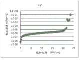
图7示出了使用TSA/氨系统沉积的SiN膜的I-V曲线。 Figure 7 shows the I-V curves of SiN films deposited using the TSA/ammonia system. the
图8示出了对于各种特征深宽比使用TSA/氨系统沉积的SiN膜的底部和侧面的阶梯覆盖性。 Figure 8 shows the bottom and side step coverage of SiN films deposited using the TSA/ammonia system for various feature aspect ratios. the
具体实施方式Detailed ways
本公开涉及SiN膜的形成,尤其涉及在半导体衬底上SiN膜的形成。本文描述的方法包括控制SiN膜中的碳含量的方法,特别是形成低碳含量的SiN膜,以及形成SiN膜的保形膜沉积(CFD)方法。 The present disclosure relates to the formation of SiN films, and more particularly to the formation of SiN films on semiconductor substrates. Methods described herein include methods to control the carbon content in SiN films, particularly to form SiN films with low carbon content, and conformal film deposition (CFD) methods to form SiN films. the
定义 definition
如本文所用的,除非另有说明,应适用下面的定义。 As used herein, unless otherwise stated, the following definitions shall apply. the
“含硅反应物”是用于制备SiN材料的试剂,单个或混合的试剂,其中该试剂含有至少一种硅化合物。该硅化合物可以是,例如,硅烷、卤代硅烷或氨基硅烷。硅烷含有氢和/或碳基团,但不含有卤素。硅烷的示例为硅烷(SiH4)、乙硅烷(Si2H6)以及有机硅烷,如甲基硅烷、乙基硅烷、异丙基硅烷、叔-丁基硅烷、二甲基硅烷、二乙基硅烷、二-叔丁基硅烷、烯丙基硅烷、仲-丁基硅烷、己基硅烷、戊基硅烷、叔丁基二硅烷、二-叔丁基二硅烷、等等。卤代硅烷含有至少一种卤素基团,并且可包含或不包含氢和/或碳的基团。卤代硅烷的示例为碘硅烷、溴硅烷、氯硅烷和氟硅烷。虽然卤代硅烷类,特别是氟硅烷,可以形成能蚀刻硅材料的反应性卤化物,但在本文所描述的某些实施方式中,等离子体被激发时含硅反应物是不存在的。特定的氯硅烷是四氯硅烷(SiCl4)、三氯硅烷(HSiCl3)、二氯硅烷(H2SiCl2)、一氯硅烷(ClSiH3)、丙基氯硅烷、甲基氯硅烷、甲基二氯硅烷、二甲基氯硅烷、乙基氯硅烷、叔丁基氯硅烷、二-叔丁基氯硅烷、异丙基氯硅烷、仲丁基氯硅烷、叔-丁基二甲基氯硅烷、叔己基二甲基氯硅烷、等。氨基硅烷包括至少一个键合到硅原子上的氮原子,但还可以含有氢原子、氧原子、卤原子和碳原子。氨基硅烷的例子是单-、二-、三-和四-氨基硅烷(分别为H3Si(NH2)4、H2Si(NH2)2、HSi(NH2)3和Si(NH2)4),以及取代的单-、二-、三-和四-氨基硅烷,例如,叔丁基氨基硅烷、甲基氨基硅烷、叔丁基硅烷基胺、双(叔丁基氨基)硅烷(SiH2(NHC(CH3)3)2(BTBAS)、叔丁基甲硅烷基氨基甲酸酯、SiH(CH3)-(N(CH3)2)2、SiHCl-(N(CH3)2)2、(Si(CH3)2NH)3、等。氨基硅烷的又一例子是三硅烷基胺(N(SiH3))。 A "silicon-containing reactant" is a reagent, single or mixed, for the preparation of SiN materials, wherein the reagent contains at least one silicon compound. The silicon compound may be, for example, a silane, halosilane or aminosilane. Silanes contain hydrogen and/or carbon groups, but no halogens. Examples of silanes are silane (SiH4 ), disilane (Si2 H6 ) and organosilanes such as methylsilane, ethylsilane, isopropylsilane, tert-butylsilane, dimethylsilane, diethylsilane Silane, di-tert-butylsilane, allylsilane, sec-butylsilane, hexylsilane, amylsilane, tert-butyldisilane, di-tert-butyldisilane, and the like. Halosilanes contain at least one halogen group and may or may not contain hydrogen and/or carbon groups. Examples of halosilanes are iodosilanes, bromosilanes, chlorosilanes and fluorosilanes. Although halosilanes, particularly fluorosilanes, can form reactive halides that etch silicon materials, in certain embodiments described herein, the plasma is ignited in the absence of silicon-containing reactants. Specific chlorosilanes are tetrachlorosilane (SiCl4 ), trichlorosilane (HSiCl3 ), dichlorosilane (H2 SiCl2 ), monochlorosilane (ClSiH3 ), propylchlorosilane, methylchlorosilane, methyl Dichlorosilane, Dimethylchlorosilane, Ethylchlorosilane, Tert-Butylchlorosilane, Di-tert-butylchlorosilane, Isopropylchlorosilane, S-butylchlorosilane, Tert-Butyldimethylchlorosilane Silane, tert-hexyldimethylchlorosilane, etc. Aminosilanes include at least one nitrogen atom bonded to a silicon atom, but may also contain hydrogen, oxygen, halogen and carbon atoms. Examples of aminosilanes are mono-, di-, tri- and tetra-aminosilanes (H3 Si(NH2 )4 , H2 Si(NH2 )2 , HSi(NH2 )3 and Si(NH2 )4 ), and substituted mono-, di-, tri- and tetra-aminosilanes such as tert-butylaminosilane, methylaminosilane, tert-butylsilylamine, bis(tert-butylamino)silane ( SiH2 (NHC(CH3 )3 )2 (BTBAS), tert-butylsilylcarbamate, SiH(CH3 )-(N(CH3 )2 )2 , SiHCl-(N(CH3 )2 )2. (Si(CH3 )2 NH)3 , etc. Yet another example of an aminosilane is trisilylamine (N(SiH3 )).
“含氮反应物”包含至少一个氮原子,例如,氨,肼,胺(带碳的胺),如甲胺、二甲胺、乙胺、异丙胺、叔丁胺、二-叔丁基胺、环丙胺、仲 丁胺、环丁胺、异戊胺、2-甲基丁-2-胺、三甲胺、二异丙基胺、二乙基异丙基胺、二-叔丁基肼,以及含芳香族胺如苯胺、吡啶、和苄胺。胺可以是伯、仲、叔或季胺(例如,四烷基胺化合物)。含氮反应物可以含有除氮以外的杂原子,例如,羟胺、叔丁羟胺和N-叔丁基羟胺是含氮反应物。 "Nitrogen-containing reactants" contain at least one nitrogen atom, for example, ammonia, hydrazine, amines (amines with carbon), such as methylamine, dimethylamine, ethylamine, isopropylamine, tert-butylamine, di-tert-butylamine, cyclic Propylamine, sec-butylamine, cyclobutylamine, isopentylamine, 2-methylbutan-2-amine, trimethylamine, diisopropylamine, diethylisopropylamine, di-tert-butylhydrazine, and Aromatic amines such as aniline, pyridine, and benzylamine. The amines can be primary, secondary, tertiary or quaternary (eg, tetraalkylamine compounds). Nitrogen-containing reactants may contain heteroatoms other than nitrogen, for example, hydroxylamine, tert-butylhydroxylamine, and N-tert-butylhydroxylamine are nitrogen-containing reactants. the
“等离子体”是指在反应室中点燃或远程地点燃并带入反应室的等离子体。等离子体可以包括本文所描述的反应物,也可以包括其他试剂,例如载气,或如氢气等反应性物类。当等离子体被激发时,反应物和其它试剂可能在反应室中存在,或远程的等离子体流入到存在反应物的室中,和/或反应物和/或载气可被远程点燃成等离子体并被带入反应室。“等离子体”是指包括任何在技术上可行的已知的等离子体,包括感应耦合等离子体和微波表面波等离子体。在本技术领域的普通技术人员将领会,技术进步会发生,因此尚未开发的等离子体发生的技术被认为在本发明的范围之内。 "Plasma" means a plasma that is ignited in a reaction chamber or ignited remotely and brought into the reaction chamber. A plasma may include the reactants described herein, but may also include other reagents, such as a carrier gas, or reactive species such as hydrogen. When the plasma is energized, reactants and other reagents may be present in the reaction chamber, or remote plasma flows into the chamber where the reactants are present, and/or the reactants and/or carrier gas may be remotely ignited into a plasma and brought into the reaction chamber. "Plasma" is meant to include any known plasma that is technically feasible, including inductively coupled plasma and microwave surface wave plasma. Those of ordinary skill in the art will appreciate that technological advances occur and thus unexplored techniques of plasma generation are considered to be within the scope of the present invention. the
“可热去除基团”是指在含氮反应物和含硅反应物中的一者或两者上的基团,这些反应物在约200℃和约550°之间分解成挥发性组分。这里所描述的非限制性的例子,如仲和叔碳基团,在此温度范围内进行消除反应。在本技术领域的普通技术人员将认识到,其他基团通过其它的机制如所描述的进行热分解,例如,叔丁氧羰基(t-BOC或“BOC”)基团通过消除机制热分解,其中该基团的叔丁基部分形成异丁烯,并该分解还形成二氧化碳。因此,可热去除基团并不限定于特定的机制或机制的组合。只要该基团在特定的温度范围内分解以产生至少一种挥发性组分,则该基团就具有资格作为可热分解的基团。例如,在给定的一组条件下,叔丁基乙胺将进行叔丁基基团的热分解以形成异丁烯,而乙基留下,因此异丁烯和乙胺是热分解的产物。在本技术领域的普通技术人员将认识到,组分的挥发性部分地取决于该组分生成的反应条件。例如,在加热和低压的条件下异丁烯可以是易挥发性的,并且可从反应室中去除,因为它不与吸附的反应物反应,同时,例如,尽管氨通常是挥发性化合物,其与吸附在衬底的表面上的含硅反应物进行反应。 "Thermally removable group" means a group on one or both of a nitrogen-containing reactant and a silicon-containing reactant that decomposes into volatile components between about 200°C and about 550°C. The non-limiting examples described here, such as secondary and tertiary carbon groups, undergo elimination reactions within this temperature range. One of ordinary skill in the art will recognize that other groups thermally decompose by other mechanisms as described, for example, the tert-butoxycarbonyl (t-BOC or "BOC") group thermally decomposes by an elimination mechanism, Wherein the tert-butyl portion of this group forms isobutene, and this decomposition also forms carbon dioxide. Thus, thermally removable groups are not limited to a particular mechanism or combination of mechanisms. A group qualifies as a thermally decomposable group as long as the group decomposes within a specified temperature range to produce at least one volatile component. For example, under a given set of conditions, tert-butylethylamine will undergo thermal decomposition of the tert-butyl group to form isobutene, leaving the ethyl group, so isobutene and ethylamine are the products of thermal decomposition. Those of ordinary skill in the art will recognize that the volatility of a component depends in part on the reaction conditions under which the component is produced. For example, isobutene can be volatile under conditions of heat and low pressure and can be removed from the reaction chamber because it does not react with the adsorbed reactants, while, for example, while ammonia is generally a volatile compound, it is not compatible with the adsorbed The silicon-containing reactants on the surface of the substrate react. the
方法 method
在此描述的是制造SiN膜的方法。在一特定实施方式中,采用 等离子激活保形膜沉积(CFD)法制造SiN膜。在一些实施方式中,采用氨基硅烷含硅反应物沉积SiN膜。在一些实施方式中,采用无卤素的氨基硅烷沉积SiN膜。在一些实施方式中,采用三硅烷基胺沉积SiN膜。 Described here is a method of fabricating a SiN film. In a specific embodiment, the SiN film is fabricated using a plasma-activated conformal film deposition (CFD) method. In some embodiments, the SiN film is deposited using an aminosilane silicon-containing reactant. In some embodiments, the SiN film is deposited using a halogen-free aminosilane. In some embodiments, the SiN film is deposited using trisilylamine. the
在一些实施方式中,采用无碳和含氮的反应物沉积SiN膜。在一些实施方式中,采用氨沉积SiN膜。在一些实施方式中,采用无碳化合物含氮反应物和含碳含氮的反应物的混合物沉积SiN膜。 In some embodiments, SiN films are deposited using carbon-free and nitrogen-containing reactants. In some embodiments, ammonia is used to deposit the SiN film. In some embodiments, the SiN film is deposited using a mixture of a carbon-free nitrogen-containing reactant and a carbon-nitrogen-containing reactant. the
在一些实施方式中,沉积得到无卤素保形SiN膜。在一些实施方式中,沉积得到无卤素和无碳保形SiN膜。在一些实施方式中,沉积得到具有经调节的应力的无卤素保形SiN膜。在一些实施方式中,在小于400℃的温度沉积得到保形SiN膜。在下文中将更详细地描述上述各个方面。 In some embodiments, deposition results in a halogen-free conformal SiN film. In some embodiments, the deposition results in a halogen-free and carbon-free conformal SiN film. In some embodiments, the deposition results in a halogen-free conformal SiN film with adjusted stress. In some embodiments, deposition at a temperature of less than 400°C results in a conformal SiN film. Each of the above aspects will be described in more detail below. the
在某些实施方式中,采用CFD沉积所述SiN膜,尽管在本文中描述的方法并不局限于CFD。其它适当的方法包括ALD,PEALD,CVD,PECVD,和等离子增强循环化学气相沉积(PECCVD)。在2011年4月11日提交的申请号为13/084,399的美国专利申请中描述了采用CFD形成薄膜的方法,该申请内容通过引用的方式被并入本文中,用于所有目的。 In certain embodiments, the SiN film is deposited using CFD, although the methods described herein are not limited to CFD. Other suitable methods include ALD, PEALD, CVD, PECVD, and plasma enhanced cyclic chemical vapor deposition (PECCVD). Methods of forming thin films using CFD are described in US Patent Application Serial No. 13/084,399, filed April 11, 2011, which is incorporated herein by reference for all purposes. the
制造半导体器件通常涉及在集成制造工艺中在非平面衬底上沉积一或多层薄膜。在所述集成工艺的一些方面,沉积保形薄膜可能是有用的。例如,可在升高的栅堆叠结构(elevated gate stack)的顶部沉积氮化硅膜作为分隔层,保护轻掺杂源和漏极区不受随后的离子注入工艺的影响。 Fabricating semiconductor devices typically involves depositing one or more thin films on non-planar substrates in an integrated fabrication process. In some aspects of the integrated process, it may be useful to deposit conformal thin films. For example, a silicon nitride film can be deposited on top of an elevated gate stack as a spacer to protect the lightly doped source and drain regions from the subsequent ion implantation process. the
在分隔层沉积工艺中,可采用化学气相沉积(CVD)法在所述非平面衬底上形成氮化硅膜,其随后进行非等向性刻蚀(anisotropically etched),形成所述分隔层。然而,随着栅堆叠结构之间的距离减小,CVD气相反应的物质传输限制(mass transport limitations)可能引起“面包块”沉积效应(“bread-loafing”deposition effects)。这些效应通常表现为在栅堆叠结构的顶面处沉积较厚而在栅堆叠结构的底角处沉积较薄。此外,由于一些模片可能具有器件密度不同的多种区域,在整个晶片表面上的物质传输影响可能导致在模片内和在晶片内的薄膜厚度发生变化。这些厚度的变化可导致一些区域过刻蚀和其它区域刻蚀不足。这可能会降低器件性能和/或模片成品率。 In the separation layer deposition process, a chemical vapor deposition (CVD) method may be used to form a silicon nitride film on the non-planar substrate, which is then anisotropically etched to form the separation layer. However, as the distance between gate stacks decreases, mass transport limitations of CVD gas phase reactions may cause "bread-loafing" deposition effects. These effects typically manifest as thicker deposits at the top of the gate stack and thinner deposits at the bottom corners of the gate stack. Furthermore, since some dies may have multiple regions with different device densities, mass transport effects across the wafer surface may result in variations in film thickness within the die and within the wafer. These thickness variations can result in overetching of some areas and underetching of others. This may degrade device performance and/or die yield. the
一些解决这些问题的方法包括原子层沉积(ALD)。ALD法与CVD法不同,CVD法采用热激活的气相反应沉积薄膜,而ALD法采用表面介导的沉积反应在逐层的基础上沉积薄膜。在ALD法的一个实施例中,包含有大量表面活性位点的衬底表面暴露于气相分布的第一反应物(A)。反应物A的一些分子在所述衬底表面的顶部形成凝聚相,所述凝聚相包括化学吸附的物质和物理吸附的反应物A分子。然后排空反应器,除去气态和物理吸附的反应物A,使得仅保留化学吸附的物质。接着向反应器中引入第二膜反应物(B),使得一些反应物B分子吸附到衬底表面。向衬底提供的热能激活吸附的反应物A和B分子之间的表面反应,形成薄膜层。最后,排空反应器,除去反应副产物和未反应的反应物B,ALD循环终止。可包括额外的ALD循环,以增加膜厚度。等离子体或其它能量形式可与加热形式配合用于衬底,或作为加热的替代方式用于衬底,以驱动反应物A和B之间的反应。 Some approaches to address these issues include atomic layer deposition (ALD). The ALD method differs from the CVD method, which uses thermally activated gas-phase reactions to deposit thin films, whereas the ALD method uses surface-mediated deposition reactions to deposit thin films on a layer-by-layer basis. In one embodiment of the ALD method, a substrate surface containing a plurality of surface active sites is exposed to a gaseous distribution of a first reactant (A). Some molecules of reactant A form a condensed phase on top of the substrate surface, the condensed phase comprising chemisorbed species and physisorbed reactant A molecules. The reactor is then evacuated to remove gaseous and physisorbed reactant A so that only chemisorbed species remain. A second film reactant (B) is then introduced into the reactor such that some reactant B molecules adsorb to the substrate surface. Thermal energy supplied to the substrate activates a surface reaction between the adsorbed reactant A and B molecules, forming a thin film layer. Finally, the reactor was evacuated to remove reaction by-products and unreacted reactant B, and the ALD cycle was terminated. Additional ALD cycles may be included to increase film thickness. Plasma or other forms of energy may be applied to the substrate in conjunction with or as an alternative to heating to drive the reaction between reactants A and B. the
根据反应物投料步骤的暴露时间以及反应物的粘附系数,在一个实施例中,各ALD循环可沉积厚度为0.5-3埃的膜层。因此,在沉积具有大于几个纳米厚度的膜时,ALD法可能是费时间的。而且,为沉积保形膜,一些反应物可能具有长的暴露时间,这也可能减少晶片吞吐量时间。 According to the exposure time of the reactant feeding step and the adhesion coefficient of the reactant, in one embodiment, each ALD cycle can deposit a film layer with a thickness of 0.5-3 angstroms. Therefore, the ALD method can be time consuming when depositing films with a thickness greater than a few nanometers. Also, to deposit conformal films, some reactants may have long exposure times, which may also reduce wafer throughput time. the
也可在平面衬底上沉积保形膜。例如,可从包含交替的膜类型的平面堆叠结构形成用于平版印刷图案应用的抗反射层。这种抗反射层的厚度可以是约100-1000埃,使得ALD法吸引力不及CVD法。然而,这种抗反射层所提供的晶片内厚度变化的公差也可能比许多CVD法所提供的更低。例如,600埃厚度的抗反射层可允许变动量为小于3埃的厚度范围。 Conformal films can also be deposited on planar substrates. For example, an antireflective layer for lithographic pattern application can be formed from a planar stack structure comprising alternating film types. The thickness of such an antireflection layer can be about 100-1000 angstroms, making the ALD method less attractive than the CVD method. However, such an anti-reflection layer may also provide a lower tolerance for intra-wafer thickness variation than many CVD methods provide. For example, an anti-reflection layer with a thickness of 600 angstroms can allow a thickness variation of less than 3 angstroms. the
在本文中描述的各种实施方式包括采用CFD沉积SiN膜。通常,CFD不依赖于在反应形成SiN之前彻底清洗一或多种反应物。例如,在轰击等离子体(或其它活化能)时,在气相中可存在一或多种反应物。因此在CFD工艺实例中,可减少或取消在ALD法中描述的一或多个工艺步骤。而且,在一些实施方式中,等离子激活的沉积反应可导致比热激活的反应更低的沉积温度,有效地降低集成工艺的热能预算。 Various embodiments described herein include depositing SiN films using CFD. In general, CFD does not rely on thorough cleaning of one or more reactants prior to reacting to form SiN. For example, upon bombardment of a plasma (or other activation energy), one or more reactants may be present in the gas phase. Thus, in the CFD process example, one or more process steps described in the ALD process can be reduced or eliminated. Furthermore, in some embodiments, plasma activated deposition reactions can result in lower deposition temperatures than thermally activated reactions, effectively reducing the thermal energy budget of the integration process. the
图1显示了在CFD工艺100中各示例性阶段的诸如惰性气体流、反应物A、反应物B以及轰击等离子体的时间之类的各种工艺参数的时 间进展。在图1中,显示了两个沉积循环110A和110B。本领域普通技术人员应理解的是,为了沉积所需的膜的厚度,在CFD工艺中可包括任意适当数量的沉积循环。示例的CFD工艺参数包括,但不限于,惰性物质和反应物质的流率,等离子体功率和频率,衬底温度,以及处理站压力。 1 shows the time progression of various process parameters, such as inert gas flow, reactant A, reactant B, and time to bombard the plasma, at various exemplary stages in a
CFD“循环”的定义与在本文中讨论的各种实施方式有关。通常一个循环是执行一次表面沉积反应所需的最少的一组操作。一个循环的结果是在衬底表面上产生至少一部分膜层。通常,一个CFD循环将仅包括:将各反应物传送并吸附至所述衬底表面,以及接着使那些吸附的反应物反应形成所述部分的膜层所必需的那些步骤。所述循环可包括某些辅助步骤,例如清除所述反应物或副产物之一,和/或处理如上沉积的部分膜。通常,一个循环仅包括一个唯一的操作顺序的例子。例如,一个循环可包括以下操作:(i)传送/吸附反应物A,(ii)传送/吸附反应物B,(iii)将B清除出反应腔室,以及(iv)施加等离子体,驱使A和B的表面反应,以在所述表面上形成所述部分的膜层。 The definition of a CFD "cycle" is relevant to various embodiments discussed herein. Usually a cycle is the minimum set of operations required to perform a surface deposition reaction. One cycle results in at least a portion of the film layer on the substrate surface. Typically, a CFD cycle will include only those steps necessary to deliver and adsorb reactants to the substrate surface, and then react those adsorbed reactants to form the portion of the film layer. The cycle may include certain auxiliary steps, such as purging one of the reactants or by-products, and/or treating a portion of the film as deposited. Usually, a loop consists of only one instance of a unique sequence of operations. For example, a cycle may include the following operations: (i) delivering/adsorbing reactant A, (ii) delivering/adsorbing reactant B, (iii) purging B from the reaction chamber, and (iv) applying plasma, driving A reacts with the surface of B to form said portion of the film layer on said surface. the
参见图1,在工艺100的所有阶段期间流通有惰性气体。在反应物A暴露阶段120A,以控制的流率将反应物A供应至处理站,以使经暴露的衬底表面饱和。反应物A可以是任意适当的沉积反应物,例如,含氮反应物。在图1中所示的实施方式中,反应物A持续流通过沉积循环110A和110B。与通常的ALD工艺不同,ALD工艺中膜前体(反应物)暴露是分开进行的,以避免气相反应,而在CFD工艺的一些实施方式中允许反应物A和B混合在气相中。与ALD工艺中反应物A的开始通入、接着稳定并暴露衬底、然后关闭以及最终移除出反应器相比较,连续供应反应物A至所述处理站,可减少或取消反应物A流率开启和稳定的时间。尽管在图1中所示的实施方式描绘了反应物A暴露阶段120A具有恒定流率,但是应理解的是在本公开内容的范围内反应物A可采用任意适当的流率,包括可变化的流率。在一些实施方式中,反应物A暴露阶段120A可具有一段持续时间,其超过反应物A的衬底表面饱和时间。例如,图1的实施方式包括在反应物A暴露阶段120A中的反应物A饱和后暴露时间130。任选地,反应物A暴露阶段120A可包括控制流率的惰性气体。示例的惰性气体包括,但不限于,氮气, 氩气,以及氦气。可提供惰性气体以协助处理站的压力和/或温度控制,液态反应物的蒸发,反应物的更快速传送和/或作为清扫气体将处理气体清除出处理站和/或处理站管道设备。 Referring to FIG. 1 , an inert gas is circulated during all stages of
在图1中所示的实施方式的反应物B暴露阶段140A,以控制的流率供应反应物B至处理站,以使暴露的衬底表面饱和。在该实施例中,反应物B可以是例如含氮的反应物。尽管在图1中所示的实施方式描绘反应物B暴露阶段140A具有恒定流率,但是应理解的是在本公开内容的范围内反应物B可采用任意适当的流率,包括可变化的流率。进一步地,应理解的是反应物B暴露阶段140A可具有任意适当的持续时间段。在一些实施方式中,反应物B暴露阶段140A可具有一段持续时间,其超过反应物B的衬底表面饱和时间。例如,图1的实施方式描绘了包括在反应物B暴露阶段140A中的反应物B饱和后暴露时间150。 In the reactant
在一些实施方式中,表面吸附的B物质可以不连续的岛状物形式存在于衬底表面上,使反应物B的表面饱和难以实现。多种表面条件可延缓反应物B在衬底表面上的成核以及饱和。例如,反应物A和/或B吸附时释放的配体可阻断一些表面活性位点,阻止进一步的反应物B的吸附。因此,在一些实施方式中,可通过在反应物B暴露阶段140A期间,调整反应物B流和/或以不连续脉冲形式发送反应物B进入处理站,提供连续的反应物B吸附层。与恒定流率情况相比,这可能会给表面吸附和解吸附过程提供额外的时间同时节约反应物B。另外,或者备选地,在一些实施方式中,在反应物B的连续暴露之间可包括一或多个清除阶段。 In some embodiments, surface-adsorbed B species may exist as discrete islands on the substrate surface, making surface saturation of reactant B difficult to achieve. Various surface conditions can retard the nucleation and saturation of reactant B on the substrate surface. For example, ligands released upon adsorption of reactants A and/or B may block some surface active sites, preventing further reactant B adsorption. Thus, in some embodiments, a continuous reactant B adsorption layer may be provided by modulating the reactant B flow and/or sending reactant B into the processing station in discrete pulses during the reactant
在等离子体激活之前,在一些实施方式中在清扫阶段160A中可从处理站除去气态反应物B。清扫处理站可避免其中反应物B对等离子体激活不稳定的气相反应或其中可能形成不需要物质的气相反应。此外,清扫处理站可除去表面吸附的配体,否则该配体可保留并污染所述膜。示例的清扫气体可包括,但不限于,氩气,氦气,和氮气。在图1中所示的实施方式中,通过连续的惰性气体流供应用于清扫阶段160A的清扫气体。在一些实施方式中清扫阶段160A可包括一或多个用于排空处理站的排空子阶段。或者,应理解的是,在一些实施方式中可省略清扫阶段160A。 Prior to plasma activation, gaseous reactant B may be removed from the processing station in a
清扫阶段160A可具有任意适当的持续时间段。在一些实施方式中,一或多种清扫气体的流率的增加可减少清扫阶段160A的持续时间。例如,可根据各种反应物的热力学特性和/或处理站和/或处理站管道(process station plumbing)的几何特征调节清扫气体流率,从而改变清扫阶段160A的持续时间。在一个非限制性实施例中,可通过调节清扫气体流率来优化清扫阶段的持续时间。这可以减少沉积循环时间,从而提高衬底吞吐量。 The
在图1中所示的实施方式的等离子体激活阶段180A,提供等离子体能,以激活在表面吸附的反应物A和B之间的表面反应。例如,等离子体可直接或间接激活反应物A的气态分子,形成反应物A自由基。然后这些自由基可与表面吸附的反应物B相互作用,导致发生成膜表面反应。等离子体激活阶段180A使沉积循环110A结束。在图1的实施方式中的沉积循环110A之后是沉积循环110B,该循环110B初始是反应物A暴露阶段120B,接着是B暴露阶段140B,清扫阶段160B以及等离子体激活阶段180B。 In the
在一些实施方式中,在等离子体激活阶段180A中点燃的等离子体可以直接在衬底表面上方形成。这可提供更大的等离子体密度,并增加反应物A和B之间的表面反应速率。例如,可通过采用两个电容耦合板向低压气体施加射频(RF)场,来产生用于CFD工艺的等离子体。可采用任意适当的气体形成等离子体。在该实施例中,诸如氩气或氦气之类的惰性气体与反应物A(含氮反应物)一起使用,形成等离子体。由RF场电离化在所述电容耦合板之间的气体,点燃等离子体,在等离子体放电区域产生自由电子。这些电子被RF场加速,并可撞击气态反应物分子。这些电子与反应物分子的撞击可形成参与沉积处理的自由基物质。应理解的是,可通过任意适当的电极耦合所述RF场。电极的非限制性实例包括处理气体分配喷头和衬底支撑基座。应理解的是,除了RF场对气体的电容耦合以外,还可采用一或多种适当的方法形成用于CFD工艺的等离子体。 In some embodiments, the plasma ignited in the
等离子体激活阶段180A可具有任意适当的持续时间。在一些实施方式中,等离子体激活阶段180A可具有一段持续时间,其超过等离子体激活的自由基与所有经暴露的衬底表面和被吸附物质相互反应并在衬底表面顶部形成连续的膜所需的时间。例如,在图1中所示的实施方式包括在等 离子体激活阶段180A中的等离子体饱和后暴露时间190。 The
在一些实施方式中,延长等离子体暴露时间和/或提供多个等离子体暴露阶段可能提供大量的反应后处理和/或沉积的膜的近表面部分。在一实施方式中,减少表面污染可制备得到用于吸附反应物A的表面。例如,由含硅反应物和含氮反应物的反应形成的氮化硅膜可具有表面,其可阻挡随后反应物的吸附。用等离子体处理所述氮化硅表面可产生氢键,有利于随后的吸附和反应事件。在本文中描述的SiN膜可暴露除了等离子体以外的处理。 In some embodiments, extending the plasma exposure time and/or providing multiple plasma exposure stages may provide substantial post-reaction treatment and/or near-surface portions of the deposited film. In one embodiment, reducing surface contamination can prepare the surface for the adsorption of reactant A. For example, a silicon nitride film formed from the reaction of a silicon-containing reactant and a nitrogen-containing reactant can have a surface that can block the adsorption of subsequent reactants. Treating the silicon nitride surface with a plasma creates hydrogen bonds that facilitate subsequent adsorption and reaction events. The SiN films described herein may be exposed to treatments other than plasma. the
在一些实施方式中,可采用除了等离子体处理以外的处理来改变如上沉积的膜的性质。这些处理包括电磁放射处理,热处理(例如,退火或高温脉冲处理),等等。任意的这些处理可单独实施,或与另一处理(包括等离子体处理)联合实施。任意的这些处理可用作为上述任意等离子体处理的替代方式。在一特定实施方式中,所述处理包括使上述膜暴露于紫外线辐射。如下文所述,在一特定实施方式中,所述方法包括在原位(即,在形成膜期间)或在沉积膜之后向膜施加UV-辐射处理。这样的处理用于减少或消除缺陷结构,并提供改善的电气性能。 In some embodiments, treatments other than plasma treatments may be employed to alter the properties of the films deposited above. These treatments include electromagnetic radiation treatments, heat treatments (eg, annealing or high temperature pulse treatments), and the like. Any of these treatments may be performed alone, or in combination with another treatment, including plasma treatment. Any of these treatments may be used as an alternative to any of the plasma treatments described above. In a particular embodiment, said treatment comprises exposing the above-mentioned film to ultraviolet radiation. As described below, in a particular embodiment, the method includes applying a UV-radiation treatment to the film either in situ (ie, during film formation) or after deposition of the film. Such treatments serve to reduce or eliminate defective structures and provide improved electrical performance. the
在某些特定实施方式中,可将UV处理与等离子体处理联合。可同时或顺序操作这两个操作。在顺序操作的选择中,可选择首先进行UV操作。在同时操作的选择中,可从不同的来源(例如,用于等离子体的RF功率源和用于UV的灯)或者从单一来源提供所述两种处理,其中所述单一来源为例如产生作为副产物的UV射线的氦气等离子体。 In certain specific embodiments, UV treatment can be combined with plasma treatment. These two operations can be performed simultaneously or sequentially. In the selection of sequential operations, you can choose to perform UV operations first. In the option of simultaneous operation, the two treatments may be provided from different sources (e.g., a source of RF power for the plasma and a lamp for the UV) or from a single source, where the single source is, for example, produced as By-products of the UV rays of the helium plasma. the
在一些实施方式中,可通过改变等离子体参数来调节诸如膜应力、介电常数、折射率、刻蚀速率之类的膜的性质。 In some embodiments, film properties such as film stress, dielectric constant, refractive index, etch rate can be tuned by changing plasma parameters. the
尽管在本文中描述的多个实施例包括两种反应物(A和B),应理解的是,在本公开内容的范围内,可采用任意适当数量的反应物。在一些实施方式中,可采用单种反应物和一种惰性气体,所述单种反应物和一种惰性气体提供用于表面反应的等离子体能。或者,一些实施方式可采用多种反应物来沉积膜。例如,在一些实施方式中,可通过含硅反应物与一或多种含氮反应物反应,或者一或多种含硅反应物与单种含氮反应物反应,或者一或多种含硅反应物和一或多种含氮反应物反应,得到氮化硅膜。 Although various embodiments described herein include two reactants (A and B), it is understood that any suitable number of reactants may be employed within the scope of the present disclosure. In some embodiments, a single reactant and an inert gas that provide plasma energy for the surface reaction may be employed. Alternatively, some embodiments may employ multiple reactants to deposit a film. For example, in some embodiments, one or more silicon-containing reactants may be reacted with one or more nitrogen-containing reactants, or one or more silicon-containing reactants may be reacted with a single nitrogen-containing reactant, or one or more silicon-containing reactants may be reacted. The reactants react with one or more nitrogen-containing reactants to form a silicon nitride film. the
在某些实施方式中,采用无卤素的含硅的反应物来沉积无卤素的SiN膜。图1提供了可用于沉积无卤素SiN膜的工艺的一个实施例,其中在图1的实施例中三硅烷基胺(TSA)用作为反应物B。虽然图1提供了沉积SiN膜的一个实施例,但是进行各种变化也是可行的。例如,在一些实施方式中,在反应物A流和B流之间,反应物A和B可与任选的清扫气体交替应用。在另一实施例中,反应物A可以是含硅反应物,而反应物B可以是含氮反应物。在一些实施方式中,可仅仅在停止含硅反应物流的时候激发等离子体。 In certain embodiments, halogen-free SiN films are deposited using halogen-free silicon-containing reactants. FIG. 1 provides an example of a process that may be used to deposit a halogen-free SiN film, where trisilylamine (TSA) is used as reactant B in the example of FIG. 1 . Although FIG. 1 provides one example of depositing a SiN film, various variations are possible. For example, in some embodiments, reactants A and B may be applied alternately with an optional purge gas between the reactant A stream and the B stream. In another example, reactant A may be a silicon-containing reactant and reactant B may be a nitrogen-containing reactant. In some embodiments, the plasma may only be ignited when the flow of silicon-containing reactants is stopped. the
在某些实施方式中,采用无卤素的含硅的反应物。在一特定实施例中,采用三硅烷基胺(TSA)作为含硅反应物。TSA是可分离的、稳定的氨基硅烷。 In certain embodiments, halogen-free silicon-containing reactants are employed. In a particular embodiment, trisilylamine (TSA) is used as the silicon-containing reactant. TSA is a separable, stable aminosilane. the
图2和3描绘了采用TSA的工艺流程200和300的实施例。首先参见图2,向反应室中提供衬底,参见205。所述衬底可以是任意适当的在其上需要SiN膜的衬底。例如,所述衬底可以是部分制造的集成电路衬底,快闪式存储器衬底或相变存储器衬底。提供的衬底可以是诸如裸硅衬底之类的裸衬底,或在其上沉积有一或多层的衬底。SiN膜要沉积到其上的表面可以是或者包括,例如,硅,多晶硅,铜,钛,钨,二氧化硅,或锗-锑-碲(GST)合金。在一些实施方式中,所述表面包括一或多个凸起或凹陷的特征。所述一或多个凸起或凹陷的特征可具有例如2:1-10:1的深宽比。所述衬底暴露于TSA,参见210。在一些实施方式中,操作210是无等离子体操作。在一些实施方式中,可对反应器加压至例如约5-50Torr范围的第一压强。在一特定实施方式中,在操作210期间的压强是约20Torr。可根据所期望的实施方式采用在该范围以外的压强。TSA被吸附到所述衬底表面上。在期望数量的TSA被吸附到所述表面上之后,停止TSA流(未图示)。然后使衬底暴露于一或多种含氮的反应物,参见215。点燃等离子体,同时在气相中存在有含氮反应物,参见220,从而在所述衬底上形成无卤素的SiN膜。在一些实施方式中,在反应器中的压强是循环的,使得在操作215和/或220期间的压强低于操作210的压强。例如,在这些操作期间的压强可以是约1-5Torr,例如是2Torr。在一些实施方式中,在操作220之后,可停止含 氮反应物流。 2 and 3 depict embodiments of process flows 200 and 300 employing TSA. Referring first to FIG. 2 , a substrate is provided into the reaction chamber, see 205 . The substrate may be any suitable substrate on which a SiN film is desired. For example, the substrate may be a partially fabricated integrated circuit substrate, a flash memory substrate or a phase change memory substrate. The provided substrate may be a bare substrate, such as a bare silicon substrate, or a substrate with one or more layers deposited thereon. The surface onto which the SiN film is deposited can be or include, for example, silicon, polysilicon, copper, titanium, tungsten, silicon dioxide, or a germanium-antimony-tellurium (GST) alloy. In some embodiments, the surface includes one or more raised or lowered features. The one or more raised or lowered features may have an aspect ratio of, for example, 2:1-10:1. The substrate is exposed to TSA, see 210. In some embodiments,
在一实施方式中,在点燃等离子体之前,通过惰性气体流和/或含氮反应物流将未吸附到衬底表面的TSA清扫出处理腔室。在另一实施方式中,可采用清扫操作除去气态含硅反应物。在一些实施方式中,在操作220之后,也可以采用清扫操作。 In one embodiment, prior to ignition of the plasma, TSA not adsorbed to the substrate surface is purged from the processing chamber by a flow of inert gas and/or nitrogen-containing reactant. In another embodiment, a sweep operation may be used to remove gaseous silicon-containing reactants. In some embodiments, after
可一或多次重复实施210-220,积聚(build up)SiN层。在一实施方式中,重复这些操作,以在所述衬底上形成约1nm-约100nm厚的保形层。在另一实施方式中,所述保形层的厚度为约5nm-约50nm。在另一实施方式中,所述保形层的厚度为约5nm-约30nm。 210-220 may be repeated one or more times to build up the SiN layer. In one embodiment, these operations are repeated to form a conformal layer about 1 nm to about 100 nm thick on the substrate. In another embodiment, the conformal layer has a thickness from about 5 nm to about 50 nm. In another embodiment, the conformal layer has a thickness from about 5 nm to about 30 nm. the
在一实施方式中,采用任意的本文所述的方法,将衬底加热至约50℃-约550℃,或更尤其是,约300℃-约450℃,例如约350℃或400℃。在一实施方式中,在沉积的整个过程中加热晶片,在其它实施方式中在沉积过程中周期性地加热晶片或者在沉积步骤之后作为退火而加热晶片。 In one embodiment, the substrate is heated to about 50°C to about 550°C, or more specifically, about 300°C to about 450°C, such as about 350°C or 400°C, using any of the methods described herein. In one embodiment, the wafer is heated throughout the deposition process, in other embodiments the wafer is heated periodically during the deposition process or as an anneal after the deposition step. the
图3描绘了工艺流程300,描绘了所述方法的实施方式的多个方面。向腔室中提供衬底,参见305。提供一或多种含氮反应物流并持续提供于整个300中,参见310。周期性地使衬底暴露于TSA,参见315。并且仅在停止TSA反应物流时周期性地点燃等离子体,参见320。在一实施方式中,通过惰性气体流和/或含氮反应物流将未吸附到衬底表面的TSA清扫出处理腔室。在另一实施方式中,可采用清扫操作。在所述等离子体处理之后,所述循环完成。可重复操作310-320多次,以积聚具有所需厚度的层。 Figure 3 depicts a
图4描绘了工艺流程400,描绘了一种方法的实施方式的多个方面。向腔室中提供衬底,参见405。形成载流,参见410。使衬底暴露于含氮反应物,参见415。使衬底暴露于含硅反应物,参见420。在停止含硅反应物流之后,点燃等离子体,参见425。该反应形成SiN。实施410-425一或多次,以积聚具有所需厚度的层。在该方法中,415和420不一定以目前的顺序实施。含氮反应物流可以是或可以不是连续的。 Figure 4 depicts a
可向任意的上述工艺加入多种额外的操作。例如,在一些实施方式中,在所有的或部分的SiN膜形成至所需的厚度之后,可使SiN膜暴露于氢气等离子体。这可从所述SiN膜除去(如果有的话)碳成分(carbon content)。在一实施方式中,采用氢气(H2)和诸如氮气、氦气或氩气之类的载气产生氢气等离子体。可采用其它的含氢气气体或由远程等离子体源产生的激活氢原子来处理所述沉积的膜。而且,在一些实施方式中,可通过改变一或多个处理脉冲的数量以及其持续时间、处理等离子体的密度、衬底温度和处理气体组合物,调节所述膜的碳成分至任意适当的浓度。 Various additional operations can be added to any of the above processes. For example, in some embodiments, after all or a portion of the SiN film is formed to a desired thickness, the SiN film may be exposed to a hydrogen plasma. This removes, if any, carbon content from the SiN film. In one embodiment, a hydrogen plasma is generated using hydrogen (H2 ) and a carrier gas such as nitrogen, helium, or argon. The deposited film can be treated with other hydrogen-containing gases or with activated hydrogen atoms generated by a remote plasma source. Also, in some embodiments, the carbon composition of the film can be adjusted to any suitable value by varying the number and duration of one or more processing pulses, the density of the processing plasma, the substrate temperature, and the processing gas composition. concentration.
无卤素的含硅的反应物 Halogen-free silicon-containing reactants
尽管图2-4提供采用TSA沉积SiN的示例性工艺流程,但是在一些实施方式中,除了采用TSA以外还采用或不是采用TSA而是采用无卤素氨基硅烷沉积其它SiN膜。所述TSA或其它氨基硅烷可以是未经取代的或是任选经任意无卤素的取代基取代的。在一些实施方式中,采用未经取代的TSA(SiH3)3N。在一些实施方式中,可采用经一或多个含碳取代基取代的TSA。含碳取代基的实例包括烷基,烯基,炔基和其它有机基团。 Although FIGS. 2-4 provide exemplary process flows for depositing SiN using TSA, in some embodiments other SiN films are deposited using halogen-free aminosilanes in addition to or instead of TSA. The TSA or other aminosilanes may be unsubstituted or optionally substituted with any halogen-free substituents. In some embodiments, unsubstituted TSA(SiH3 )3 N is employed. In some embodiments, TSA substituted with one or more carbon-containing substituents may be employed. Examples of carbon-containing substituents include alkyl, alkenyl, alkynyl and other organic groups.
无卤素的含硅的反应物的采用对于在某些衬底上沉积是有利的,其中这些衬底尤其容易受到沉积工艺的卤化物副产物的蚀刻和/或腐蚀。这些包括金属衬底,例如铜,钨,钛衬底和GST合金。例如,钨和氯化物副产物可反应形成挥发性的六氯化钨,除去位于下面的钨。在另一实施例中,氯化物气体可腐蚀铜。 The use of halogen-free silicon-containing reactants is advantageous for deposition on certain substrates that are particularly susceptible to etching and/or corrosion by halide by-products of the deposition process. These include metal substrates such as copper, tungsten, titanium substrates and GST alloys. For example, tungsten and chloride by-products can react to form volatile tungsten hexachloride, removing the underlying tungsten. In another embodiment, the chloride gas can corrode copper. the
无卤素的含硅的反应物的应用还可有利于低温(例如400℃和小于400℃)反应。这是因为含卤素的硅反应物可产生固体副产物,例如NH4Cl,其在低温反应中不能作为挥发性副产物而被清除。由于TSA在所述表面上比例如二氯硅烷(DCS)更具有反应性,因此TSA可用于低温反应。 The use of halogen-free silicon-containing reactants may also facilitate low temperature (eg, 400°C and less than 400°C) reactions. This is because halogen-containing silicon reactants can produce solid by-products, such asNH4Cl , which cannot be scavenged as volatile by-products in low temperature reactions. Since TSA is more reactive on the surface than eg dichlorosilane (DCS), TSA can be used for low temperature reactions.
在一些实施方式中,TSA可与任意适当的含氮反应物一起使用。在一实施方式中,所述含氮反应物是选自由以下组成的组:氨,肼,胺和其混合物。在一实施方式中,含氮反应物包括C1-10烷基胺或C1-10烷基胺类的混合物。在一实施方式中,所述C1-10烷基胺是一级烷基胺或二级烷基胺。在一实施方式中,所述C1-10烷基胺是一级烷基胺。在一实施方式中,所述C1-10烷基胺为如式I所示: In some embodiments, TSA may be used with any suitable nitrogen-containing reactant. In one embodiment, the nitrogen-containing reactant is selected from the group consisting of ammonia, hydrazine, amines, and mixtures thereof. In one embodiment, the nitrogen-containing reactant includes a C1-10 alkylamine or a mixture of C1-10 alkylamines. In one embodiment, the C1-10 alkylamine is a primary alkylamine or a secondary alkylamine. In one embodiment, the C1-10 alkylamine is a primary alkylamine. In one embodiment, the C1-10 alkylamine is as shown in formula I:
I I
其中R1、R2和R3各自彼此独立地为H或C1-3烷基;或R1、R2和R3中的两个与连接它们的碳原子一起形成C3-7环烷基,且R1、R2和R3中的另一个是H或C1-3烷基。在一实施方式中,所述C1-10烷基胺具有直接连接至氮原子的仲碳原子或叔碳原子。在一实施方式中,所述C1-10烷基胺是选自由以下组成的组:异丙基胺,环丙基胺,仲丁基胺,叔丁基胺,环丁基胺,异戊基胺,2-甲基-2-丁胺和己胺(thexylamine)(2,3-二甲基-2-丁胺)。在一实施方式中,在式I的C1-10烷基胺中,R1、R2和R3各自为C1-3烷基。在一实施方式中,所述C1-10烷基胺是叔丁胺(TBA)。对于上述理由,TBA是尤其有用的。 wherein R1 , R2 and R3 are each independently H or C1-3 alkyl; or two of R1 , R2 and R3 together with the carbon atoms connecting them form a C3-7 cycloalkane group, and the other of R1 , R2 and R3 is H or C1-3 alkyl. In one embodiment, the C1-10 alkylamine has a secondary or tertiary carbon atom directly attached to the nitrogen atom. In one embodiment, the C1-10 alkylamine is selected from the group consisting of isopropylamine, cyclopropylamine, sec-butylamine, tert-butylamine, cyclobutylamine, isoamylamine 2-methyl-2-butylamine and thexylamine (2,3-dimethyl-2-butylamine). In one embodiment, in the C1-10 alkylamine of formula I, R1 , R2 and R3 are each C1-3 alkyl. In one embodiment, the C1-10 alkylamine is tert-butylamine (TBA). TBA is especially useful for the above reasons.
在一些实施方式中,产生的SiN膜具有不需要的碳成分。这种在膜内的碳可能导致漏电,且可能使得所述膜不能用于一些介电质阻挡应用。碳含量可以改变,但是在一些实施方式中,约10%的碳可被认为是过高的。在本文中描述的方法解决了在SiN膜中存在有不需要的碳的问题。本文中所述的方法制造具有小于2%的碳的SiN膜,在一实施方式中得到具有小于1%的碳的SiN膜,在另一实施方式中得到具有小于0.5%的碳的SiN膜。在一些实施方式中,碳残留量的减少可以很容易在FTIR光谱中被观察到,尽管本领域普通技术人员已熟知其它的可测定在这些范围内的碳含量的分析方法。 In some embodiments, the resulting SiN film has an unwanted carbon content. This carbon within the film may cause electrical leakage and may render the film unusable for some dielectric barrier applications. The carbon content can vary, but in some embodiments, about 10% carbon can be considered too high. The methods described herein address the presence of unwanted carbon in SiN films. The methods described herein produce SiN films with less than 2% carbon, in one embodiment less than 1% carbon, and in another embodiment less than 0.5% carbon. In some embodiments, the reduction in residual carbon can be readily observed in FTIR spectroscopy, although other analytical methods are known to those of ordinary skill in the art that can determine carbon content in these ranges. the
在一些实施方式中,所述含氮反应物可包含有可热去除基团。可热去除基团是在约200℃-约550℃裂解成挥发性组分的基团。例如,仲碳基团和尤其是叔碳基团在该温度范围内可发生消除反应。在一特定实施例中,叔丁基在该温度范围内裂解,生成异丁烯。例如,在加热时,叔丁胺发生消除反应,形成异丁烯和氨。作为另一实施例,叔丁氧基羰基(t-BOC)也是在例如约150℃热分解,生成异丁烯、二氧化碳以及连接所述t-BOC基团的自由基。例如,氨基甲酸叔丁酯热分解得到异丁烯,氨和二氧化碳。 In some embodiments, the nitrogen-containing reactant may contain thermally removable groups. Thermally removable groups are groups that cleave into volatile components at about 200°C to about 550°C. For example, secondary carbon groups and especially tertiary carbon groups can undergo elimination reactions in this temperature range. In a specific embodiment, t-butyl groups are cracked within this temperature range to form isobutene. For example, upon heating, tert-butylamine undergoes an elimination reaction to form isobutene and ammonia. As another example, tert-butoxycarbonyl (t-BOC) is also thermally decomposed, eg, at about 150° C., to generate isobutylene, carbon dioxide, and free radicals attached to the t-BOC group. For example, tert-butyl carbamate is thermally decomposed to give isobutene, ammonia and carbon dioxide. the
可将衬底加热至约200℃-约550℃,使得所述基团分解并释放它们的碳成分,从而减少所述SiN膜的碳含量。所述反应物被吸附到衬底上,采用等离子体将所述反应物转化为SiN材料。可通过加热衬底除去剩余 的碳基团。可在整个沉积过程中实施所述加热,或者周期性地实施所述加热,以分解所述可热去除基团。在一实施方式中,所述衬底被加热至约200℃-约550℃,在另一实施方式中被加热至约350℃-约550℃,在另一实施方式中被加热至450℃-约550℃,以及在另一实施方式中,被加热至约450℃-约500℃。在一实施方式中,例如其中采用TBA,所述SiN膜可在约450℃-约500℃被加热约1秒-约30秒,或约1秒-约20秒,或约1秒-约10秒。虽然任意特定的热去除基团将在某一温度阈值裂解,但是采用较高的温度来增加分解的速率,和/或作为退火来改善所述SiN膜的性能。 The substrate may be heated to about 200°C to about 550°C to cause the radicals to decompose and release their carbon content, thereby reducing the carbon content of the SiN film. The reactants are adsorbed onto the substrate, and the plasma is used to convert the reactants into SiN material. Residual carbon groups can be removed by heating the substrate. The heating may be performed throughout the deposition process, or periodically to decompose the thermally removable groups. In one embodiment, the substrate is heated to about 200°C to about 550°C, in another embodiment to about 350°C to about 550°C, in another embodiment to 450°C to to about 550°C, and in another embodiment, to about 450°C to about 500°C. In one embodiment, such as where TBA is used, the SiN film may be heated at about 450° C. to about 500° C. for about 1 second to about 30 seconds, or about 1 second to about 20 seconds, or about 1 second to about 10 seconds. Second. While any particular thermal removal group will decompose at a certain temperature threshold, higher temperatures are employed to increase the rate of decomposition, and/or as an anneal to improve the properties of the SiN film. the
如上所述,所述可热去除基团可包括仲碳或叔碳官能基。含硅反应物和含氮反应物的任一种或两者可包括一或多个相同的或不同的可热去除基团。在一实施方式中,所述可热去除基团如式II所示: As noted above, the thermally removable groups may include secondary or tertiary carbon functionalities. Either or both of the silicon-containing reactant and the nitrogen-containing reactant may include one or more identical or different thermally removable groups. In one embodiment, the thermally removable group is shown in formula II:

其中R1、R2和R3各自彼此独立地为H或C1-3烷基;或R1、R2和R3中的两个与连接它们的碳原子一起形成C3-7环烷基,且R1、R2和R3中的另一个是H或C1-3烷基;和其中在作为含氮反应物的部分时,每一个所述可热去除基团连接至所述含氮反应物的氮或氧,以及,在作为含硅反应物的部分时,每一个所述可热去除基团连接至所述含硅反应物的硅或氮或氧。在一实施方式中,R1、R2和R3各自彼此独立地为C1-3烷基。在一实施方式中,所述可热去除基团是叔丁基。 wherein R1 , R2 and R3 are each independently H or C1-3 alkyl; or two of R1 , R2 and R3 together with the carbon atoms connecting them form a C3-7 cycloalkane and the other of R1 , R2 and R3 is H or C1-3 alkyl; and wherein each of said thermally removable groups is attached to said nitrogen or oxygen of a nitrogen-containing reactant, and, when part of a silicon-containing reactant, each of said thermally removable groups is attached to silicon or nitrogen or oxygen of said silicon-containing reactant. In one embodiment, R1 , R2 and R3 are each independently C1-3 alkyl. In one embodiment, the thermally removable group is t-butyl.
无碳含氮的反应物 Carbon-free and nitrogen-containing reactants
在一些实施方式中,所述含氮反应物是无碳含氮的反应物。实施例包括氨和肼。例如,在一些实施方式中,采用TSA和氨分别作为含硅反应物和含氮反应物,用于沉积SiN。 In some embodiments, the nitrogen-containing reactant is a carbon-free nitrogen-containing reactant. Examples include ammonia and hydrazine. For example, in some embodiments, TSA and ammonia are employed as silicon-containing reactants and nitrogen-containing reactants, respectively, for depositing SiN. the
在一些实施方式中,例如采用无碳含氮的反应物沉积用于快闪式存储器的SiO2/SiN/SiO2(又称为ONO堆叠结构(ONO stack)))的SiN膜。沉积的膜可以是无卤素且无碳的,不存在有甚至痕量的卤素或碳(除非 其来源于污染源,诸如人类或者在沉积工具中的在先工艺之后的不充分清洁)。 In some embodiments, for example, a SiN film of SiO2 /SiN/SiO2 (also known as an ONO stack) for flash memory is deposited using a carbon-free and nitrogen-containing reactant. The deposited film can be halogen-free and carbon-free, with not even traces of halogen or carbon present (unless it originates from a contamination source such as humans or insufficient cleaning after a prior process in the deposition tool).
调节应力和湿法刻蚀速率 Adjusting stress and wet etch rate
在一些实施方式中,可选择含氮反应物来调节沉积的SiN膜的应力和/或湿法刻蚀速率。例如,可采用氨或其它无碳含氮的反应物来沉积具有高的湿法刻蚀速率的拉伸膜。 In some embodiments, nitrogen-containing reactants can be selected to adjust the stress and/or wet etch rate of the deposited SiN film. For example, ammonia or other carbon-free and nitrogen-containing reactants can be used to deposit stretched films with high wet etch rates. the
在另一实施例中,可采用TBA或其它含碳含氮反应物来沉积耐刻蚀压缩膜(etch resistant,compressive films)。 In another embodiment, TBA or other carbon- and nitrogen-containing reactants may be used to deposit etch resistant, compressive films. the
在一些实施方式中,可采用两种含氮反应物来调节所需的膜的应力。例如,可采用含碳含氮反应物(例如TBA)和无碳含氮反应物(例如氨)来沉积具有所需应力和湿法刻蚀速率的SiN膜。在一些实施方式中,这些含氮反应物可与TSA一起使用,以沉积具有所需应力和湿法刻蚀速率的无氯SiN膜。 In some embodiments, two nitrogen-containing reactants can be used to adjust the desired film stress. For example, carbon- and nitrogen-containing reactants such as TBA and carbon-free nitrogen-containing reactants such as ammonia can be used to deposit SiN films with desired stress and wet etch rates. In some embodiments, these nitrogen-containing reactants can be used with TSA to deposit chlorine-free SiN films with desired stress and wet etch rates. the
在这种方法中,可获得具有范围是-4GPa(压缩)至2GPa(拉伸)的应力的SiN膜。例如,在一些实施方式中,通过采用纯TBA的含氮反应物流(或其它含碳含氮反应物流)可获得具有约-4GPa至约-2GPa的应力的压缩SiN膜。在一些实施方式中,通过采用纯氨的含氮反应物流(或其它无碳含氮反应物流)可获得具有约1GPa至约2GPa的应力的拉伸SiN膜。在一些实施方式中,通过采用TBA(或其它含碳含氮反应物)和氨(或其它无碳含氮反应物)的混合物可获得具有约-2GPa至1GPa的应力的SiN膜。 In this method, SiN films with stress ranging from -4 GPa (compressive) to 2 GPa (tensile) can be obtained. For example, in some embodiments, a compressive SiN film having a stress of about -4 GPa to about -2 GPa can be obtained by employing a nitrogen-containing reactant stream of pure TBA (or other carbon- and nitrogen-containing reactant stream). In some embodiments, a stretched SiN film having a stress of about 1 GPa to about 2 GPa can be obtained by employing a nitrogen-containing reactant stream of pure ammonia (or other carbon-free nitrogen-containing reactant stream). In some embodiments, a SiN film having a stress of about -2 GPa to 1 GPa can be obtained by employing a mixture of TBA (or other carbon- and nitrogen-containing reactant) and ammonia (or other carbon-free nitrogen-containing reactant). the
可根据特定实施方式以及包括在本文所述多种工艺的等离子体阶段期间的RF功率和等离子体持续时间的工艺条件,改变通过采用纯TBA(或其它含碳含氮反应物)、纯氨(或其它无碳含氮反应物)和这些物质的混合物而获得的应力值。更长且更高功率等离子体可制造更压缩的SiN膜。在一些实施方式中,采用TSA和仅无碳含氮反应物(例如氨和/或肼)沉积得到的SiN膜可通过适当地调整RF功率而被调节为具有例如-0.5GPa的轻微压缩的应力至高达2GPa的拉伸应力。 By using pure TBA (or other carbon- and nitrogen-containing reactants), pure ammonia ( or other carbon-free and nitrogen-containing reactants) and mixtures of these substances. Longer and higher power plasmas can produce more compressive SiN films. In some embodiments, SiN films deposited using TSA and only carbon-free nitrogen-containing reactants (e.g., ammonia and/or hydrazine) can be tuned to have a slightly compressive stress, e.g., -0.5 GPa, by appropriately adjusting the RF power. Up to tensile stress up to 2GPa. the
在一些实施方式中,例如,可采用TSA和无碳含氮反应物、约0.15W/cm2的HFRF功率沉积得到拉伸(1-2GPa)SiN膜,采用TSA和无碳 含氮反应物以及接近1W/cm2的HFRF功率沉积得到轻微压缩的SiN膜。(RF功率以W/衬底面积表示,例如一个300mm的晶片具有约706cm2的面积)。通过添加TBA或其它含碳含氮反应物可制造更为压缩的膜。在一些情况下,采用TBA可能难于形成拉伸膜,这是因为要采用相对高的RF功率来分解所述TBA分子的叔丁基。因此,采用诸如氨或肼之类的无碳含氮反应物来获得拉伸膜是有利的。所述RF等离子体是仅HF等离子体,尽管在一些其它实施方式中,可添加LF功率。 In some embodiments, for example, stretched (1-2 GPa) SiN films can be deposited using TSA and carbon-free and nitrogen-containing reactants at an HFRF power of about 0.15 W/cm2 , using TSA and carbon-free and nitrogen-containing reactants and HFRF powers close to 1 W/cm2 deposited slightly compressed SiN films. (RF power is expressed in W/substrate area, eg a 300mm wafer has an area of about706cm2 ). More compact membranes can be made by adding TBA or other carbon and nitrogen containing reactants. In some cases, it may be difficult to form stretched films using TBA because of the relatively high RF power used to decompose the tert-butyl groups of the TBA molecule. Therefore, it is advantageous to employ carbon-free nitrogen-containing reactants such as ammonia or hydrazine to obtain stretched films. The RF plasma is an HF only plasma, although in some other embodiments LF power may be added.
采用TSA和无碳反应物体系可获得的湿法刻蚀的范围也大于传统的工艺。例如针对采用TSA/氨沉积得到的SiN膜的热氧化物湿法刻蚀速度比率(WERR)对如上所述的低HFRF功率可以是约2.0。增加HFRF功率至约1W/cm2或以上可使WERR降低至约0.5。这可与范围是约0.1至1.0的DCS/TBA体系的WERR相比拟。 The range of wet etching achievable with TSA and carbon-free reactant systems is also greater than conventional processes. For example, the thermal oxide wet etch rate ratio (WERR) for SiN films deposited using TSA/ammonia may be about 2.0 for low HFRF power as described above. Increasing the HFRF power to about 1 W/cm2 or above can reduce the WERR to about 0.5. This is comparable to the WERR for DCS/TBA systems ranging from about 0.1 to 1.0.
低温下沉积 deposition at low temperature
如前所述,因为TSA在表面比例如二氯甲硅烷等活性更高,所以TSA可用于低温反应。另外,在一些实施方式中,相较于TBA或其他的含氮反应物,无碳含氮反应物在低温下能沉积高质量SiN膜。例如,DCS/TBA系统,由于在TBA分子中叔丁基基团裂解动力学差,在400℃及以下的温度开始表现出侧壁沉积下降。 As mentioned earlier, TSA can be used for low temperature reactions because it is more reactive on the surface than, for example, dichlorosilane. Additionally, in some embodiments, the carbon-free nitrogen-containing reactants can deposit high quality SiN films at lower temperatures compared to TBA or other nitrogen-containing reactants. For example, the DCS/TBA system, due to the poor kinetics of cleavage of the tert-butyl group in the TBA molecule, starts to show a decrease in sidewall deposition at temperatures of 400 °C and below. the
在一些实施方式中,使用无卤素氨基硅烷和无碳含氮反应物的SiN沉积能够在明显低于可以使用DCS/TBA及类似系统的温度下提供高质量SiN膜。例如,TSA/氨在350℃,和400℃或450℃的温度下提供高质量沉积。相应地,在一些实施方式中,TSA能够与一种或者多种无碳含氮反应物在50℃至450℃,或50℃至400℃,或50℃至350℃的温度范围内一起使用。 In some embodiments, SiN deposition using halogen-free aminosilanes and carbon-free nitrogen-containing reactants can provide high-quality SiN films at temperatures significantly lower than can be used with DCS/TBA and similar systems. For example, TSA/Ammonia provides high quality deposition at temperatures of 350°C, and 400°C or 450°C. Accordingly, in some embodiments, TSA can be used with one or more carbon-free nitrogen-containing reactants at a temperature ranging from 50°C to 450°C, or from 50°C to 400°C, or from 50°C to 350°C. the
保形膜 Conformal film
根据各种各样的实施方式,本文描述的方法能够提供SiN膜,该SiN膜与其沉积的衬底表面是高度共形的。在一些实施方式中,阶梯覆盖率(step coverage)至少为90%。用于本说明书的目的,“阶梯覆盖率”定义为 沉积膜的两个厚度的比率,底部阶梯覆盖率是特征底部厚度与特征顶部厚度之比,侧壁阶梯覆盖率是特征侧壁的厚度与特征顶部厚度之比。 According to various embodiments, the methods described herein can provide SiN films that are highly conformal to the substrate surface on which they are deposited. In some embodiments, the step coverage is at least 90%. For the purposes of this specification, "step coverage" is defined as the ratio of the two thicknesses of the deposited film, bottom step coverage is the ratio of the thickness of the bottom of the feature to the thickness of the top of the feature, and sidewall step coverage is the ratio of the thickness of the sidewall of the feature to the thickness of the top of the feature. Ratio of feature top thicknesses. the
设备 equipment
本发明的另一方面是设置成能完成本文描述的方法的设备。合适的设备包括完成工艺操作的硬件,以及具有用于控制根据本发明的工艺操作的指令的系统控制器。 Another aspect of the invention is an apparatus configured to perform the methods described herein. Suitable equipment includes hardware to perform process operations, and a system controller having instructions for controlling process operations in accordance with the present invention. the
可以理解的是,上述一个或多个实施方式中可以使用任何合适的处理站。例如,图5示意地显示了CFD处理站1300。为了简便起见,CFD处理站1300描述成单独的处理站,其具有用于维持低压环境的操作腔室体1302。然而,可以理解的是,在通常的低压操作工具环境下,可以包括多个CFD处理站1300。虽然在图5中描述的实施方式显示为一个处理站,可以理解的是,在一些实施方式中,在操作工具中可以包括多个处理站。例如,图6描述了多站的操作工具2400的实施方式。另外,可以理解的是,在一些实施方式中,CFD处理站1300的一个或多个硬件参数,包括下文详细讨论的那些,可以被一个或者多个计算机控制器程序化(programmatically)调节。 It will be appreciated that any suitable processing station may be used in one or more of the embodiments described above. For example, FIG. 5 schematically shows a
CFD处理站1300与用于传输操作气体给散布喷头(distribution showerhead)1306的反应物传输系统1301呈流体连接。反应物传输系统1301包括混合容器(mixing vessel)1304用于混合和/或对传输到喷头1306的操作气体进行状态调整。一或多个混合容器入口阀1320控制将操作气体导入混合容器1304。 The
一些反应物在汽化并随后传输到处理站之前,可以以液态形式存储。例如,图5的设备包括汽化点(vaporization point)1303用于汽化拟传输到混合容器1304中去的液态反应物。在一些实施方式中,汽化点1303可以是加热汽化器。这些汽化器产生的饱和反应物蒸汽可以在下游的传输管道中冷凝。不相容的气体暴露在冷凝的反应物中会产生小颗粒。这些小颗粒会堵塞管道、妨碍阀门运行、污染衬底,等等。解决这些问题的一些方法包括清扫和/或疏通传输管道以去除残留的反应物。然而,清扫传输管道会增加处理站循环时间,降低处理站产量。因此,在一些实施方式中,汽化点1303的下 游传输管道是伴热的(heat traced)。在一些实施方式中,混合容器1304也是伴热的。在一个非限制性的实施方式中,汽化点1303的下游传输管道具有升高的温度分步,温度自约100℃升高至在混合容器1304的约150℃。 Some reactants may be stored in liquid form before being vaporized and subsequently transported to a processing station. For example, the apparatus of FIG. 5 includes a vaporization point 1303 for vaporizing liquid reactants to be transferred to a
在一些实施方式中,液态反应物在液体喷射器中汽化。例如,液体喷射器可以以脉冲的形式把液态反应物喷射到混合容器上游的载体气流中。在一些实施方式中,液体喷射器通过迅速把液体从较高的压力到较低的压力来汽化反应物。可以理解的是,较小的液滴比较大的液滴汽化更快,从而减少液体喷射和完全汽化之间的时间。较快的汽化可以减小汽化点1303下游传输管道的长度。在一个实施方式中,液体喷射器直接安装到混合容器1304上。在另一个实施方式中,液体喷射器直接安装到喷头1306上。 In some embodiments, liquid reactants are vaporized in a liquid injector. For example, a liquid injector may inject liquid reactants in pulses into the carrier gas stream upstream of the mixing vessel. In some embodiments, the liquid injector vaporizes the reactants by rapidly passing a liquid from a higher pressure to a lower pressure. It is understood that smaller droplets vaporize faster than larger droplets, thereby reducing the time between liquid ejection and complete vaporization. Faster vaporization can reduce the length of transfer piping downstream of vaporization point 1303 . In one embodiment, the liquid injector is mounted directly to the
在一些实施方式中,汽化点1303上游提供有液体流控制器,用于为汽化并传输到处理站1300而控制液体质量流。在一个实施方式中,液体流控制器(LFC)包括位于LFC下游的热式质量流量计(MFM)。LFC柱塞阀的调节是响应于由正比-积分-微分控制器(PID)在与MFM电气通讯中提供的反馈控制信号。然而,使用反馈控制来稳定液体流可能需要1秒或者更多。这可能延长用于液态反应物的定量给料的时间。因此,在一些实施方式中,LFC在反馈控制模式和直接控制模式之间动态切换。在一些实施方式中,通过禁止LFC的传感管和PID控制器,LFC从反馈控制模式动态切换至直接控制模式。 In some embodiments, a liquid flow controller is provided upstream of vaporization point 1303 for controlling liquid mass flow for vaporization and delivery to
喷头1306向衬底1312散布操作气体。在图5所示的实施方式中,衬底1312位于喷头1306下方,且显示被搁在基座1308上。可以理解的是,为了把操作气体散布到衬底1312,喷头1306可以具有任何合适的形状,且可以具有任何合适的数量和端口安排。 The
在一些实施方式中,微腔(microvolume)1307位于喷头1306下方。在微腔中而不是在处理站整个空间执行CFD操作,可以减少反应物的暴露和清扫时间,可以减少用于改变CFD操作条件(例如,压力,温度等)的时间,可以限制处理站机器人在操作气体中的暴露,等等。示例性的微腔体积包括但不限于,体积为0.1升和2升之间。 In some embodiments, a
在一些实施方式中,基座1308可以被抬升或降低以使得衬底 1312暴露在微腔1307中和/或改变微腔1307的体积。例如,在衬底转移相,基座1308被降低以使得衬底1312装载到基座1308上。在CFD操作相,基座1308被抬升以使得把衬底放置在微腔1307中。在一些实施方式中,微腔1307完全围绕衬底1312以及部分基座1308,以在CFD操作中创设出高流阻区域。 In some embodiments, the
可选地,在CFD操作期间,基座1308可以在微腔1307内被降低和/或抬升以调节操作压力、反应物浓度等。在一个实施方式中,在CFD操作过程中,操作腔室体1302维持在基础压力,把基座1308降低以使得微腔1307被排空。微腔相对于操作腔室体积的示例性比例,包括但不限于,体积比在1:500至1:10之间。可以理解的是,在一些实施方式中,基座高度可以通过合适的计算机控制器程序化调节。 Optionally,
在另一个实施方式中,对基座1308高度的调节使得等离子体密度在CFD操作中的等离子体激活和/或处理周期是可变的。在CFD操作相结束时,基座1308在另一个衬底转移相中降低,以使得衬底1312从基座1308中移除。 In another embodiment, the adjustment of the height of the
虽然本文所描述的示例微腔变化是高度可调的基座,可以理解的是,在一些实施方式中,可以相对于基座1308调整喷头1306位置,以改变微腔1307的体积。此外,可以理解的是,基座1308和/或喷头1306的垂直位置可以通过任何合适的机制改变。本领域普通技术人员可以理解的是,这样的机制包括,例如,液压装置,气动装置,弹簧机构,螺线管,等等。在一些实施方式中,基座1308可包括一个旋转机构,例如,沿着与衬底表面垂直的轴,用于旋转衬底1312的方向。可以理解的是,在一些实施方式中,一个或多个这些示例性的调整可以通过一个或多个合适的计算机控制器以编程方式执行。 While the example microcavity variation described herein is a height-adjustable pedestal, it will be appreciated that in some embodiments, the position of the
回到图5所示的实施方式,喷头1306和基座1308与RF功率源1314和匹配网络1316电气连接用于给等离子体供电。在一些实施方式中,通过控制一个或多个处理站压力、气体浓度、RF源功率、RF源频率、和等离子体电源脉冲计时器来控制等离子体能量。例如,RF功率源1314和匹配网络1316可以用任何合适的功率操作以形成具有所需要自由基种类组合的等 离子体。合适的功率的例子包括但不限于,介于100W至5000W之间的功率。同样地,RF功率源1314可提供任何合适频率的RF功率。在一些实施方式中,RF功率源1314可设置成控制相互独立的高频率和低频率RF功率源。低频率RF频率的例子可包括但不限于,介于50kHz和500kHz之间的频率。高频率RF频率的例子可包括但不限于,介于1.8MHz和2.45GHz之间的频率。可以理解的是,可以离散地或者连续地调节任何适合的参数以提供等离子体能量用于表面反应。在一个非限制性的实施方式中,相较于连续功率的等离子体,等离子体功率可以是间歇地脉冲形式,以减少衬底表面的离子轰击。 Returning to the embodiment shown in Figure 5, the
在一些实施方式中,通过一个或更多的等离子体监视器对等离子体进行原位监测。在一个实施方式中,通过一个或多个的电压、电流传感器(例如,VI探针)对等离子体功率进行监测。在另一实施方式中,通过一个或多个发射光谱传感器(OES)对等离子体密度和/或操作气体浓度进行测量。在一些实施方式中,基于这些原位等离子体监视器的测量值,对一个或多个等离子体参数进行程序化调节。例如,OES传感器可在反馈回路中使用,用于提供对等离子体功率的程序化(programmatic)控制。可以理解的是,在一些实施方式中,其他监视器可以用来监测等离子体和其它工序的特征。这些监视器包括,但不限于,红外(IR)监视器、声学监视器、和压力传感器。 In some embodiments, the plasma is monitored in situ by one or more plasma monitors. In one embodiment, plasma power is monitored by one or more voltage and current sensors (eg, VI probes). In another embodiment, the plasma density and/or operating gas concentration is measured by one or more optical emission sensors (OES). In some embodiments, one or more plasma parameters are programmed to be adjusted based on the measurements of these in situ plasma monitors. For example, OES sensors can be used in a feedback loop to provide programmatic control of plasma power. It will be appreciated that in some embodiments other monitors may be used to monitor plasma and other process characteristics. These monitors include, but are not limited to, infrared (IR) monitors, acoustic monitors, and pressure sensors. the
在一些实施方式中,等离子体是通过输入/输出控制(IOC)排序指令来控制。例如,用于为等离子体操作相设置等离子体条件的指令可以被包括在相应的CFD操作配方的等离子体活化配方相中。在一些实施方式中,可依次排列操作配方相,从而使所有用于CFD操作相的指令与该操作相同步地执行。可以理解的是,等离子体产生的一些方面可以具有特征明显的瞬态和/或稳定的时间,这有可能延长等离子体操作相。换句话说,这样的时间延迟是可预期的。这种时间延迟可以包括激发等离子体的时间和在指示功率设置稳定等离子体的时间。 In some embodiments, the plasma is controlled through input/output control (IOC) sequenced instructions. For example, instructions for setting plasma conditions for a plasma operating phase may be included in a plasma activation recipe phase of a corresponding CFD operating recipe. In some embodiments, the operational recipe phases may be sequenced such that all instructions for a CFD operational phase are executed synchronously with that operation. It will be appreciated that some aspects of plasma generation may have well-characterized transient and/or settling times, which may prolong the plasma operating phase. In other words, such time delays are expected. This time delay may include the time to ignite the plasma and the time to stabilize the plasma at the indicated power setting. the
在一些实施方式中,基座1308可以通过加热器1310控制温度。另外,在一些实施方式中,可以通过蝶形阀1318提供对CFD处理站1300的 压力控制。如图5所示,蝶形阀1318作为由下游真空泵(未显示)提供的真空的节流阀。然而,在一些实施方式中,处理站1300的压力控制可以通过改变导入到CFD处理站1300的一种或者多种气体的流速来调节。 In some embodiments, the
如上所述,多站操作工具可以包括一个或多个处理站。图6显示了多站操作工具2400的示意图,该多站操作工具2400具有内装载锁2402和外装载锁2404,装载锁的任一个或这两者都可能包括远程等离子体源。机械手2406,在大气压力下,被配置为经由大气端口2410通过吊舱(pod)2408装载的盒把晶片移入内装载锁2402。通过机械手2406把晶片放置在内装载锁2402的基座2412上,该大气端口2410关闭,且装载锁向下泵送。当内装载锁2402包括远程等离子体源时,晶片在导入到操作室2414之前,可暴露于装载锁中的远程等离子体处理。另外,也可以在装载锁2402内加热晶片,例如,以除去水分和吸附气体。接着,至操作室2414的腔室传输端口2416打开,并且另一个机械手(未示出)把晶片放置到第一站的基座上的反应器中用于后续处理。虽然图6中所示的实施方式包括装载锁,可以理解的是,在一些实施方式中,可以提供晶片直接进入到处理站的方式。 As noted above, a multi-station operation tool may include one or more processing stations. Figure 6 shows a schematic diagram of a
所描述的操作室2414包括四个处理站,在图6所示的实施方式中,编号从1到4。每个站都有一个加热基座(2418处所示用于站1),和气体管线入口。可以理解的是,在一些实施方式中,每个处理站可具有不同的目的或多个目的。例如,在一些实施方式中,处理站可以在CFD操作模式和PECVD操作模式之间切换。另外地或备选地,在一些实施方式中,操作室2414可以包括一个或多个配对的CFD和PECVD处理站。虽然示出的操作室2414包括四个站,可以理解的是,根据本发明公开的操作室可具有任何合适数量的站。例如,在一些实施方式中,操作室可以具有五个或更多个站,而在其它实施方式中的操作室可以具有三个或更少的站。 The depicted
图6还描绘了在操作室2414内传输晶片的晶片处理系统2490。在一些实施方式中,晶片操作系统2490可以在各种处理站之间和/或在处理站和装载锁之间传输晶片。可以理解的是,可以采用任何适当的晶片操作系统。非限制性实施方式包括晶片转盘和晶片处理机械手。图6描述了系统控制器2450,用于控制操作工具2400的操作条件和硬件状态。系统控制器 2450可包括一个或多个存储设备2456,一个或多个大容量存储设备2454,和一个或多个处理器2452。处理器2452可以包括CPU或计算机,模拟和/或数字输入/输出接头,步进电机控制器板,等等。 FIG. 6 also depicts
在一些实施方式中,系统控制器2450控制操作工具2400的所有活动。系统控制器2450执行存储在大容量存储设备2454中的、加载到存储设备2456的和在处理器2452上执行的系统控制软件2458。系统控制软件2458可包括用于控制计时、气体混合、腔室和/或站压力、腔室和/或站温度、晶片温度、目标功率水平、RF功率水平、衬底基座、夹盘和/或感受器(susceptor)位置、和由操作工具2400执行的特定工艺的其他参数。系统控制软件2458可以以任何合适的方式配置。例如,可以编写各种操作工具组件的子程序或控制对象用于控制操作工具组件执行各种操作工具操作所必须的操作。可以以任何合适的计算机可读的编程语言编码系统控制软件2458。 In some embodiments,
在一些实施方式中,系统控制软件2458可包括输入/输出控制(IOC)排序指令,用于控制上面描述的各种参数。例如,CFD操作的各相可以包括用于由系统控制器2450执行的一个或多个指令。相应的CFD配方相可以包括用于设定CFD操作相操作条件的指令。在一些实施方式中,CFD配方相可以依次排列,从而使得用于CFD操作相的所有指令与该操作相同步执行。 In some embodiments,
在一些实施方式中可以采用与系统控制器2450相关联的、存储在大容量存储设备2454和/或存储设备2456上的、其他计算机软件和/或程序。用于此目的的示例性程序或部分程序包括衬底定位程序、操作气体控制程序、压力控制程序、加热器控制程序和等离子体控制程序。 Other computer software and/or programs stored on
衬底定位程序可以包括用于操作工具组件的程序代码,该操作工具组件把衬底装载到基座2418且控制衬底和操作工具2400其他部件之间的距离。 The substrate positioning program may include program code for the handling tool assembly that loads the substrate onto the
操作气体控制程序可以包括代码,该代码用于控制气体成分和流速,且可选地用于在沉积之前把气体通入一个或者多个处理站以便稳定处理站压力。压力控制程序可包括通过调节例如处理站的排放系统内的节流阀和进入处理站的气流等来控制处理站内的压力。 The operating gas control program may include code for controlling gas composition and flow rate, and optionally for passing gas to one or more process stations prior to deposition to stabilize process station pressure. The pressure control procedure may include controlling the pressure within the processing station by adjusting, for example, a throttle valve in the discharge system of the processing station, the gas flow into the processing station, and the like. the
加热器控制程序可以包括用于控制加热单元电流的代码,该加热单元用于加热衬底。可选地,加热器控制程序可以控制热传输气体(例如氦气)传输到衬底。 The heater control program may include code for controlling current to a heating unit for heating the substrate. Optionally, a heater control program can control the delivery of a heat transfer gas (eg, helium) to the substrate. the
等离子体控制程序可以包括代码,其用于设置应用到一个或者多个处理站中操作电极的RF功率水平。 The plasma control program may include code for setting the RF power levels applied to the operating electrodes in one or more processing stations. the
在一些实施方式中,可以有与系统控制器2450相关的用户界面。该用户界面可以包括显示屏、设备和/或操作条件的图解软件显示、及用户输入装置,例如定点设备、键盘、触摸屏、麦克风,等等。 In some implementations, there may be a user interface associated with the
在一些实施方式中,由系统控制器2450调整的参数可能涉及操作条件。非限制性例子包括操作气体成分和流速、温度、压力、等离子体条件(如RF偏置功率水平)、压力、温度,等等。这些参数可以以配方的形式提供给用户,这可利用用户界面输入。 In some implementations, the parameters adjusted by the
用于监测操作的信号可以从各种操作工具传感器由系统控制器2450的模拟和/或数字输入接头提供。用于控制操作的信号可以在操作工具2400的模拟和数字输出接头输出。可被监测的操作工具传感器的非限制性例子包括质量流量控制器、压力传感器(如压力计)、热电偶、等等。来自这些传感器的数据可以与适当地程序化的反馈和控制算法一起使用,以维持操作条件。 Signals for monitoring operation may be provided by analog and/or digital input connections of
系统控制器2450可提供用于实现上述的沉积方法的程序指令。该程序指令可以控制各种工艺参数,例如DC功率水平、RF偏压功率水平、压力、温度、等等。该指令可以根据本文所描述的各种实施方式,控制用于操作膜堆叠原位沉积的参数。 The
典型地,系统控制器包括一个或多个存储设备和一个或多个处理器,其被配置为执行指令,以使得该装置执行根据本发明的方法。包含用于控制根据本发明的工艺操作的指令的机器可读介质,可以被耦合到系统控制器。 Typically, the system controller includes one or more memory devices and one or more processors configured to execute instructions such that the apparatus performs a method according to the invention. A machine-readable medium containing instructions for controlling the operation of a process according to the present invention may be coupled to a system controller. the
图案化方法/设备 Patterning method/equipment
本文描述的设备/方法可以与光刻图案化(lithographic patterning)工具或方法联用,例如,用于半导体设备、显示器、LED、光电板等等的制造和生产。通常,但不是必定,这样的工具/方法将和普通的制造设施一起使用或操作。膜的光刻图案化通常包括部分或所有的以下步骤,每一步骤用一些可能的工具启动:(1)使用旋涂或喷涂工具在工件(即,衬底)上施用光刻胶;(2)使用热板或炉或UV固化工具固化光刻胶;(3)使用晶片分档器(wafer stepper)等工具将光刻胶在可见光或紫外线或X-射线下曝光;(4)使用诸如湿法工作台(wet bench)等工具,对抗蚀剂进行显影,以便选择性地除去抗蚀剂,从而进行图案化;(5)通过使用干的或等离子体辅助蚀刻工具,将光致抗蚀图案(resist pattern)转移到基底膜或工件上;和(6)使用诸如RF或微波等离子体抗蚀剂剥离器(microwave plasma resist stripper.)等工具,去除抗蚀剂。在一个实施方式中,SiN膜使用如本文所述的方法形成。SiN膜用于,例如,本文所述的目的之一。此外,该方法包括如上所述的步骤(1)-(6)中一个或多个。 The apparatus/methods described herein can be used in conjunction with lithographic patterning tools or methods, eg, for the fabrication and production of semiconductor devices, displays, LEDs, photovoltaic panels, and the like. Typically, but not necessarily, such tools/methods will be used or operated with common manufacturing facilities. Photolithographic patterning of films typically involves some or all of the following steps, each initiated with some possible tool: (1) applying photoresist on the workpiece (i.e., substrate) using a spin-coating or spraying tool; (2) ) using a hot plate or oven or UV curing tool to cure the photoresist; (3) using a tool such as a wafer stepper (wafer stepper) to expose the photoresist to visible light or ultraviolet light or X-rays; (4) using tools such as wet (wet bench) and other tools to develop the resist to selectively remove the resist for patterning; (5) by using dry or plasma-assisted etching tools to pattern the photoresist (resist pattern) transferred to the base film or workpiece; and (6) using tools such as RF or microwave plasma resist stripper (microwave plasma resist stripper.), etc., to remove the resist. In one embodiment, the SiN film is formed using methods as described herein. SiN films are used, for example, for one of the purposes described herein. In addition, the method includes one or more of the above-mentioned steps (1)-(6). the
实施例 Example
参照下面的实施例进一步理解本发明,下面的实施例的目的纯粹是示例性的。另外,本发明的范围并不限于所示的实施例,实施例仅仅旨在说明本发明的单个方面。在功能上等同的任何方法,落入本发明的范围之内。除了本文所描述的那些,对于本领域技术人员来说,从前面的描述和附图出发,对本发明所做的各种各样的修改是显而易见的。此外,这样的修改都落入所附权利要求的范围。 The invention can be further understood by reference to the following examples, which are intended to be purely illustrative. Additionally, the scope of the present invention is not limited to the illustrated embodiments, which are intended to illustrate a single aspect of the invention. Any methods that are functionally equivalent are intended to be within the scope of this invention. Various modifications to the invention in addition to those described herein will become apparent to those skilled in the art from the foregoing description and accompanying drawings. Moreover, such modifications all fall within the scope of the appended claims. the
实施例1 Example 1
表1包括了一些反应伙伴(reaction partners),以及可能用于根据本文所描述的实施例制备SiN膜的温度和压力参数。 Table 1 includes some reaction partners, as well as temperature and pressure parameters that may be used to prepare SiN films according to the examples described herein. the


方法A使用TSA作为含硅反应物,用氨作为含氮反应物。根据正在被处理衬底的要求,温度范围为50℃至约550℃。RF功率的范围可以从约0.15W/cm2至约3W/cm2,以便如上所述调整应力。 Method A uses TSA as the silicon-containing reactant and ammonia as the nitrogen-containing reactant. Depending on the requirements of the substrate being processed, the temperature ranges from 50°C to about 550°C. The RF power can range from about 0.15 W/cm2 to about 3 W/cm2 to adjust the stress as described above.
方法B是方法A的一个具体例子,在一个较低的温度下,约50℃和450℃之间(这取决于对热预算的考量),使用TSA和氨沉积拉伸SiN膜。例如,具有铜膜的衬底,可在小于约400℃的温度下处理,以防止铜晶粒结构的改变。例如,GST合金,可以在温度大约350℃-375℃处理。如上所述,TSA和氨可用来在这些较低的温度下在合理的沉积速率下提供具有高阶梯覆盖率的高品质膜。RF功率相对较低以实现拉伸膜。 Method B is a specific example of Method A, using TSA and ammonia to deposit stretched SiN films at a lower temperature, between about 50°C and 450°C (depending on thermal budget considerations). For example, a substrate having a copper film may be processed at a temperature of less than about 400°C to prevent changes in the copper grain structure. For example, GST alloys can be processed at temperatures around 350°C - 375°C. As noted above, TSA and ammonia can be used to provide high quality films with high step coverage at these lower temperatures at reasonable deposition rates. The RF power was relatively low to achieve stretching of the film. the
方法C是方法A的另一具体例子,在一个较低的温度下,约300℃和400℃之间(这取决于对热预算的考量),使用TSA和氨沉积拉伸SiN膜。该温度范围可用于在包括铜、GST合金、和其他热敏感材料的衬底上沉积SiN膜,同时保持较高的沉积速率。 Method C is another specific example of Method A, using TSA and ammonia to deposit stretched SiN films at a lower temperature, between about 300°C and 400°C (depending on thermal budget considerations). This temperature range can be used to deposit SiN films on substrates including copper, GST alloys, and other thermally sensitive materials while maintaining high deposition rates. the
方法D是方法A的另一具体例子,且与方法C类似,除了使用更高的RF功率以便沉积更高压缩的膜。 Method D is another specific example of Method A, and is similar to Method C, except that higher RF power is used in order to deposit a more compressive film. the
方法E-H是使用氨和TBA的混合物作为含氮反应物以便调整所沉积的SiN膜的应力和湿法刻蚀速率的例子。在一个实施例中,方法E可以与诸如方法D那样的较高RF水平、与TBA一起使用,TBA的存在会使膜具有更高的压缩。 Methods E-H are examples of using a mixture of ammonia and TBA as a nitrogen-containing reactant in order to tune the stress and wet etch rate of the deposited SiN film. In one embodiment, Method E can be used with higher RF levels, such as Method D, with TBA, the presence of which would result in a higher compressibility of the film. the
方法I是使用TSA和TBA分别作为含硅和含氮反应物的方法的例子。例如,方法I可以用于沉积压缩的无卤素SiN膜。 Method I is an example of a method using TSA and TBA as silicon- and nitrogen-containing reactants, respectively. For example, Method I can be used to deposit compact halogen-free SiN films. the
在上述方法实施例中,诸如肼等无碳含氮反应物可用于替代氨,或者在氨之外使用。如上所述,其他的含碳反应物可用于替代TBA,或者在TBA之外使用。 In the above method embodiments, a carbon-free nitrogen-containing reactant such as hydrazine may be used in place of or in addition to ammonia. As noted above, other carbon-containing reactants can be used in place of, or in addition to, TBA. the
实施例2 Example 2
300毫米晶片放入真空室。在该室内,该晶片由铝质基座支撑,该铝质基座在整个操作过程中被加热。例如,该基座加热到约50℃至约550℃之间的一个恒定温度。三硅烷基胺(TSA)作为约0.25slm至约5slm(标准升每分钟)之间的气相流被引入到反应器中约1秒至约30秒之间,以把TSA吸附到晶片表面上。TSA流停止后,用惰性气体流清扫反应器中的剩余气相TSA和任何副产物。然后,在反应器中建立约1slm至约10slm之间的氨气相流约1秒至约30秒之间。一种等离子体,例如,13.56MHz,功率150W,在晶片的上方点燃约1秒至约15秒之间。在反应器中的惰性气体流清扫剩余的气相氨和任何副产物。重复TSA流、惰性气体清扫、氨流、等离子体和惰性气体清扫,以沉积具有所需厚度的SiN膜。每个循环沉积约0.5埃至约1.5埃之间的SiN膜。 A 300 mm wafer is placed into the vacuum chamber. Inside the chamber, the wafer is supported by an aluminum susceptor that is heated throughout the operation. For example, the susceptor is heated to a constant temperature between about 50°C and about 550°C. Trisilylamine (TSA) is introduced into the reactor as a gas phase flow of between about 0.25 slm to about 5 slm (standard liters per minute) between about 1 second and about 30 seconds to adsorb TSA onto the wafer surface. After the flow of TSA was stopped, the reactor was purged with a flow of inert gas for remaining gas-phase TSA and any by-products. An ammonia gas phase flow of between about 1 slm to about 10 slm is then established in the reactor for between about 1 second to about 30 seconds. A plasma, eg, 13.56 MHz at 150 W, is ignited over the wafer for between about 1 second and about 15 seconds. The inert gas flow in the reactor sweeps the remaining gas phase ammonia and any by-products. The TSA flow, inert gas sweep, ammonia flow, plasma, and inert gas sweep are repeated to deposit a SiN film with the desired thickness. Each cycle deposits between about 0.5 Angstroms and about 1.5 Angstroms of SiN film. the
可替代地,1-5slm的TBA可以用于替代氨,或者在氨之外使用。 Alternatively, 1-5 slm of TBA can be used in place of, or in addition to, ammonia. the
在另一种替代方案,在CFD运行中,氨流(和/或TBA流)连续运行。在这些运行中,使用如上所述的相同的条件,除了首先建立并维持氨流。以与上述相同的速率和时间,把TSA流导入到反应器中,接着如上所述用惰性气体清扫。等离子体如上所述被点燃,接着如上述的惰性气体清扫。重复TSA流、惰性气体清扫、等离子体点燃和惰性气体清扫,以沉积具有所需厚度的SiN膜。每个所述的循环沉积约0.5埃至约1.5埃之间的SiN膜。 In another alternative, the ammonia stream (and/or the TBA stream) is run continuously during the CFD run. In these runs, the same conditions were used as described above, except that the ammonia flow was first established and maintained. A stream of TSA was introduced into the reactor at the same rate and time as above, followed by purging with inert gas as described above. The plasma is ignited as described above, followed by an inert gas sweep as described above. The TSA flow, inert gas sweep, plasma ignition, and inert gas sweep are repeated to deposit a SiN film with the desired thickness. Each of the cycles deposits between about 0.5 Angstroms and about 1.5 Angstroms of SiN film. the
实施例3 Example 3
如实施例2中所描述的方法,通过使用TSA和氨在450℃温度下沉积SiN膜。图7显示了沉积膜的I-V曲线。值得一提的是,SiN膜在高达约22MV/cm的施加电场不会破裂。图8显示了各种特征深宽比的底部和侧面阶梯覆盖率。 As described in Example 2, SiN films were deposited at a temperature of 450° C. by using TSA and ammonia. Figure 7 shows the I-V curves of the deposited films. It is worth mentioning that the SiN film does not rupture up to an applied electric field of about 22 MV/cm. Figure 8 shows the bottom and side step coverage for various feature aspect ratios. the
沉积SiN膜的方法使用以下系统:DCS/TBA,TSA/TBA和 TSA/氨。每种膜的折射率是DCS/TBA:1.83,TSA/TBA:1.83,TSA/氨:1.90。 The methods for depositing SiN films used the following systems: DCS/TBA, TSA/TBA and TSA/Ammonia. The refractive index of each film was DCS/TBA: 1.83, TSA/TBA: 1.83, TSA/ammonia: 1.90. the
出于清楚地理解的目的,虽然前面已经描述了一些细节,显然的是,在所附权利要求的范围内可以作出一定的改变和修改。应当注意的是,有许多替代的方式来实施所述的方法、系统和装置。因此,所述的实施方式应被视为说明性的,而不是限制性的。 While certain details have been described above for purposes of clarity of understanding, it will be evident that certain changes and modifications may be made within the scope of the appended claims. It should be noted that there are many alternative ways of implementing the described methods, systems and apparatus. Accordingly, the described embodiments should be regarded as illustrative rather than restrictive. the
Claims (24)
Applications Claiming Priority (4)
| Application Number | Priority Date | Filing Date | Title |
|---|---|---|---|
| US201261588964P | 2012-01-20 | 2012-01-20 | |
| US61/588,964 | 2012-01-20 | ||
| US13/414,619US8592328B2 (en) | 2012-01-20 | 2012-03-07 | Method for depositing a chlorine-free conformal sin film |
| US13/414,619 | 2012-03-07 |
Publications (1)
| Publication Number | Publication Date |
|---|---|
| CN103225071Atrue CN103225071A (en) | 2013-07-31 |
Family
ID=47709842
Family Applications (1)
| Application Number | Title | Priority Date | Filing Date |
|---|---|---|---|
| CN2013100214608APendingCN103225071A (en) | 2012-01-20 | 2013-01-21 | Method for depositing a chlorine-free conformal SiN film |
Country Status (7)
| Country | Link |
|---|---|
| US (3) | US8592328B2 (en) |
| EP (1) | EP2618365A3 (en) |
| JP (2) | JP6635640B2 (en) |
| KR (1) | KR20130085900A (en) |
| CN (1) | CN103225071A (en) |
| SG (2) | SG10201505472UA (en) |
| TW (1) | TWI609426B (en) |
Cited By (17)
| Publication number | Priority date | Publication date | Assignee | Title |
|---|---|---|---|---|
| CN105448701A (en)* | 2014-09-24 | 2016-03-30 | 朗姆研究公司 | Method and apparatus for uniformly reducing the characteristic wet etch rate of a silicon nitride film |
| CN105849221A (en)* | 2013-09-27 | 2016-08-10 | 乔治洛德方法研究和开发液化空气有限公司 | Amine substituted trisilylamine and tridisilylamine compounds |
| CN108028171A (en)* | 2015-09-18 | 2018-05-11 | 应用材料公司 | Low temperature conformal deposit of the silicon nitride on high aspect ratio structure |
| US10074543B2 (en) | 2016-08-31 | 2018-09-11 | Lam Research Corporation | High dry etch rate materials for semiconductor patterning applications |
| US10134579B2 (en) | 2016-11-14 | 2018-11-20 | Lam Research Corporation | Method for high modulus ALD SiO2 spacer |
| US10141505B2 (en) | 2015-09-24 | 2018-11-27 | Lam Research Corporation | Bromine containing silicon precursors for encapsulation layers |
| US10269559B2 (en) | 2017-09-13 | 2019-04-23 | Lam Research Corporation | Dielectric gapfill of high aspect ratio features utilizing a sacrificial etch cap layer |
| US10454029B2 (en) | 2016-11-11 | 2019-10-22 | Lam Research Corporation | Method for reducing the wet etch rate of a sin film without damaging the underlying substrate |
| CN110846636A (en)* | 2018-08-20 | 2020-02-28 | 应用材料公司 | Coating material for processing chamber |
| US10629435B2 (en) | 2016-07-29 | 2020-04-21 | Lam Research Corporation | Doped ALD films for semiconductor patterning applications |
| TWI695082B (en)* | 2014-11-24 | 2020-06-01 | 美商蘭姆研究公司 | Method of depositing ammonia free and chlorine free conformal silicon nitride film |
| US10804099B2 (en) | 2014-11-24 | 2020-10-13 | Lam Research Corporation | Selective inhibition in atomic layer deposition of silicon-containing films |
| US10832908B2 (en) | 2016-11-11 | 2020-11-10 | Lam Research Corporation | Self-aligned multi-patterning process flow with ALD gapfill spacer mask |
| US11404275B2 (en) | 2018-03-02 | 2022-08-02 | Lam Research Corporation | Selective deposition using hydrolysis |
| US12157945B2 (en) | 2019-08-06 | 2024-12-03 | Lam Research Corporation | Thermal atomic layer deposition of silicon-containing films |
| US12237175B2 (en) | 2019-06-04 | 2025-02-25 | Lam Research Corporation | Polymerization protective liner for reactive ion etch in patterning |
| US12412742B2 (en) | 2020-07-28 | 2025-09-09 | Lam Research Corporation | Impurity reduction in silicon-containing films |
Families Citing this family (441)
| Publication number | Priority date | Publication date | Assignee | Title |
|---|---|---|---|---|
| US10378106B2 (en) | 2008-11-14 | 2019-08-13 | Asm Ip Holding B.V. | Method of forming insulation film by modified PEALD |
| US9394608B2 (en) | 2009-04-06 | 2016-07-19 | Asm America, Inc. | Semiconductor processing reactor and components thereof |
| US8802201B2 (en) | 2009-08-14 | 2014-08-12 | Asm America, Inc. | Systems and methods for thin-film deposition of metal oxides using excited nitrogen-oxygen species |
| US9257274B2 (en) | 2010-04-15 | 2016-02-09 | Lam Research Corporation | Gapfill of variable aspect ratio features with a composite PEALD and PECVD method |
| US20110256734A1 (en) | 2010-04-15 | 2011-10-20 | Hausmann Dennis M | Silicon nitride films and methods |
| US8956983B2 (en) | 2010-04-15 | 2015-02-17 | Novellus Systems, Inc. | Conformal doping via plasma activated atomic layer deposition and conformal film deposition |
| US9892917B2 (en) | 2010-04-15 | 2018-02-13 | Lam Research Corporation | Plasma assisted atomic layer deposition of multi-layer films for patterning applications |
| US9997357B2 (en) | 2010-04-15 | 2018-06-12 | Lam Research Corporation | Capped ALD films for doping fin-shaped channel regions of 3-D IC transistors |
| US8637411B2 (en) | 2010-04-15 | 2014-01-28 | Novellus Systems, Inc. | Plasma activated conformal dielectric film deposition |
| US9076646B2 (en) | 2010-04-15 | 2015-07-07 | Lam Research Corporation | Plasma enhanced atomic layer deposition with pulsed plasma exposure |
| US9373500B2 (en) | 2014-02-21 | 2016-06-21 | Lam Research Corporation | Plasma assisted atomic layer deposition titanium oxide for conformal encapsulation and gapfill applications |
| US9611544B2 (en) | 2010-04-15 | 2017-04-04 | Novellus Systems, Inc. | Plasma activated conformal dielectric film deposition |
| US9390909B2 (en) | 2013-11-07 | 2016-07-12 | Novellus Systems, Inc. | Soft landing nanolaminates for advanced patterning |
| US9685320B2 (en) | 2010-09-23 | 2017-06-20 | Lam Research Corporation | Methods for depositing silicon oxide |
| US8647993B2 (en) | 2011-04-11 | 2014-02-11 | Novellus Systems, Inc. | Methods for UV-assisted conformal film deposition |
| US9312155B2 (en) | 2011-06-06 | 2016-04-12 | Asm Japan K.K. | High-throughput semiconductor-processing apparatus equipped with multiple dual-chamber modules |
| US10364496B2 (en) | 2011-06-27 | 2019-07-30 | Asm Ip Holding B.V. | Dual section module having shared and unshared mass flow controllers |
| US10854498B2 (en) | 2011-07-15 | 2020-12-01 | Asm Ip Holding B.V. | Wafer-supporting device and method for producing same |
| US20130023129A1 (en) | 2011-07-20 | 2013-01-24 | Asm America, Inc. | Pressure transmitter for a semiconductor processing environment |
| US9017481B1 (en) | 2011-10-28 | 2015-04-28 | Asm America, Inc. | Process feed management for semiconductor substrate processing |
| US8592328B2 (en) | 2012-01-20 | 2013-11-26 | Novellus Systems, Inc. | Method for depositing a chlorine-free conformal sin film |
| US9659799B2 (en) | 2012-08-28 | 2017-05-23 | Asm Ip Holding B.V. | Systems and methods for dynamic semiconductor process scheduling |
| US10714315B2 (en) | 2012-10-12 | 2020-07-14 | Asm Ip Holdings B.V. | Semiconductor reaction chamber showerhead |
| KR102207992B1 (en) | 2012-10-23 | 2021-01-26 | 램 리써치 코포레이션 | Sub-saturated atomic layer deposition and conformal film deposition |
| SG2013083241A (en) | 2012-11-08 | 2014-06-27 | Novellus Systems Inc | Conformal film deposition for gapfill |
| JP6538300B2 (en) | 2012-11-08 | 2019-07-03 | ノベラス・システムズ・インコーポレーテッドNovellus Systems Incorporated | Method for depositing a film on a sensitive substrate |
| US9512519B2 (en)* | 2012-12-03 | 2016-12-06 | Taiwan Semiconductor Manufacturing Company, Ltd. | Atomic layer deposition apparatus and method |
| US20160376700A1 (en) | 2013-02-01 | 2016-12-29 | Asm Ip Holding B.V. | System for treatment of deposition reactor |
| US9589770B2 (en) | 2013-03-08 | 2017-03-07 | Asm Ip Holding B.V. | Method and systems for in-situ formation of intermediate reactive species |
| US9484191B2 (en) | 2013-03-08 | 2016-11-01 | Asm Ip Holding B.V. | Pulsed remote plasma method and system |
| US9824881B2 (en) | 2013-03-14 | 2017-11-21 | Asm Ip Holding B.V. | Si precursors for deposition of SiN at low temperatures |
| US9564309B2 (en) | 2013-03-14 | 2017-02-07 | Asm Ip Holding B.V. | Si precursors for deposition of SiN at low temperatures |
| US20150020974A1 (en)* | 2013-07-19 | 2015-01-22 | Psk Inc. | Baffle and apparatus for treating surface of baffle, and substrate treating apparatus |
| US9240412B2 (en) | 2013-09-27 | 2016-01-19 | Asm Ip Holding B.V. | Semiconductor structure and device and methods of forming same using selective epitaxial process |
| US9214334B2 (en) | 2014-02-18 | 2015-12-15 | Lam Research Corporation | High growth rate process for conformal aluminum nitride |
| US10683571B2 (en) | 2014-02-25 | 2020-06-16 | Asm Ip Holding B.V. | Gas supply manifold and method of supplying gases to chamber using same |
| US10167557B2 (en) | 2014-03-18 | 2019-01-01 | Asm Ip Holding B.V. | Gas distribution system, reactor including the system, and methods of using the same |
| US11015245B2 (en) | 2014-03-19 | 2021-05-25 | Asm Ip Holding B.V. | Gas-phase reactor and system having exhaust plenum and components thereof |
| US10858737B2 (en) | 2014-07-28 | 2020-12-08 | Asm Ip Holding B.V. | Showerhead assembly and components thereof |
| US9548188B2 (en) | 2014-07-30 | 2017-01-17 | Lam Research Corporation | Method of conditioning vacuum chamber of semiconductor substrate processing apparatus |
| US9478438B2 (en) | 2014-08-20 | 2016-10-25 | Lam Research Corporation | Method and apparatus to deposit pure titanium thin film at low temperature using titanium tetraiodide precursor |
| US9478411B2 (en) | 2014-08-20 | 2016-10-25 | Lam Research Corporation | Method to tune TiOx stoichiometry using atomic layer deposited Ti film to minimize contact resistance for TiOx/Ti based MIS contact scheme for CMOS |
| US9890456B2 (en) | 2014-08-21 | 2018-02-13 | Asm Ip Holding B.V. | Method and system for in situ formation of gas-phase compounds |
| US9576792B2 (en) | 2014-09-17 | 2017-02-21 | Asm Ip Holding B.V. | Deposition of SiN |
| US9657845B2 (en) | 2014-10-07 | 2017-05-23 | Asm Ip Holding B.V. | Variable conductance gas distribution apparatus and method |
| US10941490B2 (en) | 2014-10-07 | 2021-03-09 | Asm Ip Holding B.V. | Multiple temperature range susceptor, assembly, reactor and system including the susceptor, and methods of using the same |
| JP6236709B2 (en)* | 2014-10-14 | 2017-11-29 | 大陽日酸株式会社 | Silicon nitride film manufacturing method and silicon nitride film |
| US9640371B2 (en)* | 2014-10-20 | 2017-05-02 | Lam Research Corporation | System and method for detecting a process point in multi-mode pulse processes |
| KR102263121B1 (en) | 2014-12-22 | 2021-06-09 | 에이에스엠 아이피 홀딩 비.브이. | Semiconductor device and manufacuring method thereof |
| US9474163B2 (en)* | 2014-12-30 | 2016-10-18 | Asm Ip Holding B.V. | Germanium oxide pre-clean module and process |
| US9490116B2 (en)* | 2015-01-09 | 2016-11-08 | Applied Materials, Inc. | Gate stack materials for semiconductor applications for lithographic overlay improvement |
| US10658222B2 (en) | 2015-01-16 | 2020-05-19 | Lam Research Corporation | Moveable edge coupling ring for edge process control during semiconductor wafer processing |
| EP3247688A4 (en)* | 2015-01-23 | 2018-01-24 | Hewlett-Packard Development Company, L.P. | Susceptor materials for 3d printing using microwave processing |
| US10373850B2 (en) | 2015-03-11 | 2019-08-06 | Asm Ip Holding B.V. | Pre-clean chamber and process with substrate tray for changing substrate temperature |
| US10529542B2 (en) | 2015-03-11 | 2020-01-07 | Asm Ip Holdings B.V. | Cross-flow reactor and method |
| US10276355B2 (en) | 2015-03-12 | 2019-04-30 | Asm Ip Holding B.V. | Multi-zone reactor, system including the reactor, and method of using the same |
| US10566187B2 (en) | 2015-03-20 | 2020-02-18 | Lam Research Corporation | Ultrathin atomic layer deposition film accuracy thickness control |
| US11124876B2 (en) | 2015-03-30 | 2021-09-21 | L'Air Liquide, Société Anonyme pour l'Etude et l'Exploitation des Procédés Georges Claude | Si-containing film forming precursors and methods of using the same |
| US9777025B2 (en) | 2015-03-30 | 2017-10-03 | L'Air Liquide, Société pour l'Etude et l'Exploitation des Procédés Georges Claude | Si-containing film forming precursors and methods of using the same |
| US9502238B2 (en) | 2015-04-03 | 2016-11-22 | Lam Research Corporation | Deposition of conformal films by atomic layer deposition and atomic layer etch |
| US10458018B2 (en) | 2015-06-26 | 2019-10-29 | Asm Ip Holding B.V. | Structures including metal carbide material, devices including the structures, and methods of forming same |
| US10600673B2 (en) | 2015-07-07 | 2020-03-24 | Asm Ip Holding B.V. | Magnetic susceptor to baseplate seal |
| US10526701B2 (en) | 2015-07-09 | 2020-01-07 | Lam Research Corporation | Multi-cycle ALD process for film uniformity and thickness profile modulation |
| US10957561B2 (en) | 2015-07-30 | 2021-03-23 | Lam Research Corporation | Gas delivery system |
| US10410857B2 (en) | 2015-08-24 | 2019-09-10 | Asm Ip Holding B.V. | Formation of SiN thin films |
| US9837286B2 (en) | 2015-09-04 | 2017-12-05 | Lam Research Corporation | Systems and methods for selectively etching tungsten in a downstream reactor |
| KR102080114B1 (en)* | 2015-09-21 | 2020-02-24 | 주식회사 원익아이피에스 | Method of fabricating nitride film |
| US9960072B2 (en) | 2015-09-29 | 2018-05-01 | Asm Ip Holding B.V. | Variable adjustment for precise matching of multiple chamber cavity housings |
| US10192751B2 (en) | 2015-10-15 | 2019-01-29 | Lam Research Corporation | Systems and methods for ultrahigh selective nitride etch |
| US10211308B2 (en) | 2015-10-21 | 2019-02-19 | Asm Ip Holding B.V. | NbMC layers |
| US10322384B2 (en) | 2015-11-09 | 2019-06-18 | Asm Ip Holding B.V. | Counter flow mixer for process chamber |
| JP6544232B2 (en)* | 2015-12-25 | 2019-07-17 | 東京エレクトロン株式会社 | Film forming method and film forming apparatus |
| KR102458309B1 (en) | 2015-12-28 | 2022-10-24 | 삼성전자주식회사 | Method of forming a SiOCN material layer and method of fabricating a semiconductor device |
| US11139308B2 (en) | 2015-12-29 | 2021-10-05 | Asm Ip Holding B.V. | Atomic layer deposition of III-V compounds to form V-NAND devices |
| US10825659B2 (en) | 2016-01-07 | 2020-11-03 | Lam Research Corporation | Substrate processing chamber including multiple gas injection points and dual injector |
| DE102016200506B4 (en)* | 2016-01-17 | 2024-05-02 | Robert Bosch Gmbh | Etching device and etching process |
| US9640409B1 (en) | 2016-02-02 | 2017-05-02 | Lam Research Corporation | Self-limited planarization of hardmask |
| JP2017139297A (en)* | 2016-02-02 | 2017-08-10 | 東京エレクトロン株式会社 | Film growth method and film growth apparatus |
| US10224235B2 (en) | 2016-02-05 | 2019-03-05 | Lam Research Corporation | Systems and methods for creating airgap seals using atomic layer deposition and high density plasma chemical vapor deposition |
| US10651015B2 (en) | 2016-02-12 | 2020-05-12 | Lam Research Corporation | Variable depth edge ring for etch uniformity control |
| US10147588B2 (en) | 2016-02-12 | 2018-12-04 | Lam Research Corporation | System and method for increasing electron density levels in a plasma of a substrate processing system |
| US10699878B2 (en) | 2016-02-12 | 2020-06-30 | Lam Research Corporation | Chamber member of a plasma source and pedestal with radially outward positioned lift pins for translation of a substrate c-ring |
| US10438833B2 (en) | 2016-02-16 | 2019-10-08 | Lam Research Corporation | Wafer lift ring system for wafer transfer |
| US10529554B2 (en) | 2016-02-19 | 2020-01-07 | Asm Ip Holding B.V. | Method for forming silicon nitride film selectively on sidewalls or flat surfaces of trenches |
| US10468251B2 (en) | 2016-02-19 | 2019-11-05 | Asm Ip Holding B.V. | Method for forming spacers using silicon nitride film for spacer-defined multiple patterning |
| US10501866B2 (en) | 2016-03-09 | 2019-12-10 | Asm Ip Holding B.V. | Gas distribution apparatus for improved film uniformity in an epitaxial system |
| WO2017154202A1 (en) | 2016-03-11 | 2017-09-14 | 大陽日酸株式会社 | Method for producing silicon nitride film, and silicon nitride film |
| US10343920B2 (en) | 2016-03-18 | 2019-07-09 | Asm Ip Holding B.V. | Aligned carbon nanotubes |
| US9892913B2 (en) | 2016-03-24 | 2018-02-13 | Asm Ip Holding B.V. | Radial and thickness control via biased multi-port injection settings |
| JP6710089B2 (en)* | 2016-04-04 | 2020-06-17 | 東京エレクトロン株式会社 | Method for forming tungsten film |
| US10190213B2 (en) | 2016-04-21 | 2019-01-29 | Asm Ip Holding B.V. | Deposition of metal borides |
| US10865475B2 (en) | 2016-04-21 | 2020-12-15 | Asm Ip Holding B.V. | Deposition of metal borides and silicides |
| US10262858B2 (en) | 2016-04-25 | 2019-04-16 | Applied Materials, Inc. | Surface functionalization and passivation with a control layer |
| US10367080B2 (en) | 2016-05-02 | 2019-07-30 | Asm Ip Holding B.V. | Method of forming a germanium oxynitride film |
| US10032628B2 (en) | 2016-05-02 | 2018-07-24 | Asm Ip Holding B.V. | Source/drain performance through conformal solid state doping |
| US10157736B2 (en) | 2016-05-06 | 2018-12-18 | Lam Research Corporation | Methods of encapsulation |
| KR102592471B1 (en) | 2016-05-17 | 2023-10-20 | 에이에스엠 아이피 홀딩 비.브이. | Method of forming metal interconnection and method of fabricating semiconductor device using the same |
| EP3459118A4 (en)* | 2016-05-17 | 2020-01-15 | The Government Of The United States Of America As The Secretary of The Navy | PASSIVATION BY CHEMICAL VAPOR DEPOSIT ASSISTED BY PLASMA WITHOUT DAMAGE TO HIGH ELECTRONIC MOBILITY TRANSISTORS IN ALGAN / GAN |
| US11453943B2 (en) | 2016-05-25 | 2022-09-27 | Asm Ip Holding B.V. | Method for forming carbon-containing silicon/metal oxide or nitride film by ALD using silicon precursor and hydrocarbon precursor |
| US10388509B2 (en) | 2016-06-28 | 2019-08-20 | Asm Ip Holding B.V. | Formation of epitaxial layers via dislocation filtering |
| US9773643B1 (en) | 2016-06-30 | 2017-09-26 | Lam Research Corporation | Apparatus and method for deposition and etch in gap fill |
| US10062563B2 (en) | 2016-07-01 | 2018-08-28 | Lam Research Corporation | Selective atomic layer deposition with post-dose treatment |
| US10612137B2 (en) | 2016-07-08 | 2020-04-07 | Asm Ip Holdings B.V. | Organic reactants for atomic layer deposition |
| US9859151B1 (en) | 2016-07-08 | 2018-01-02 | Asm Ip Holding B.V. | Selective film deposition method to form air gaps |
| US10714385B2 (en) | 2016-07-19 | 2020-07-14 | Asm Ip Holding B.V. | Selective deposition of tungsten |
| US9929006B2 (en) | 2016-07-20 | 2018-03-27 | Micron Technology, Inc. | Silicon chalcogenate precursors, methods of forming the silicon chalcogenate precursors, and related methods of forming silicon nitride and semiconductor structures |
| KR102354490B1 (en) | 2016-07-27 | 2022-01-21 | 에이에스엠 아이피 홀딩 비.브이. | Method of processing a substrate |
| KR102532607B1 (en) | 2016-07-28 | 2023-05-15 | 에이에스엠 아이피 홀딩 비.브이. | Substrate processing apparatus and method of operating the same |
| US9887082B1 (en) | 2016-07-28 | 2018-02-06 | Asm Ip Holding B.V. | Method and apparatus for filling a gap |
| US9812320B1 (en) | 2016-07-28 | 2017-11-07 | Asm Ip Holding B.V. | Method and apparatus for filling a gap |
| US10395919B2 (en) | 2016-07-28 | 2019-08-27 | Asm Ip Holding B.V. | Method and apparatus for filling a gap |
| US9865456B1 (en) | 2016-08-12 | 2018-01-09 | Micron Technology, Inc. | Methods of forming silicon nitride by atomic layer deposition and methods of forming semiconductor structures |
| US10410832B2 (en) | 2016-08-19 | 2019-09-10 | Lam Research Corporation | Control of on-wafer CD uniformity with movable edge ring and gas injection adjustment |
| KR102613349B1 (en) | 2016-08-25 | 2023-12-14 | 에이에스엠 아이피 홀딩 비.브이. | Exhaust apparatus and substrate processing apparatus and thin film fabricating method using the same |
| US10037884B2 (en) | 2016-08-31 | 2018-07-31 | Lam Research Corporation | Selective atomic layer deposition for gapfill using sacrificial underlayer |
| US9865455B1 (en) | 2016-09-07 | 2018-01-09 | Lam Research Corporation | Nitride film formed by plasma-enhanced and thermal atomic layer deposition process |
| JP6568508B2 (en) | 2016-09-14 | 2019-08-28 | 株式会社Kokusai Electric | Semiconductor device manufacturing method, substrate processing apparatus, and program |
| US9824884B1 (en) | 2016-10-06 | 2017-11-21 | Lam Research Corporation | Method for depositing metals free ald silicon nitride films using halide-based precursors |
| US10410943B2 (en) | 2016-10-13 | 2019-09-10 | Asm Ip Holding B.V. | Method for passivating a surface of a semiconductor and related systems |
| US10643826B2 (en) | 2016-10-26 | 2020-05-05 | Asm Ip Holdings B.V. | Methods for thermally calibrating reaction chambers |
| US11532757B2 (en) | 2016-10-27 | 2022-12-20 | Asm Ip Holding B.V. | Deposition of charge trapping layers |
| US10229833B2 (en) | 2016-11-01 | 2019-03-12 | Asm Ip Holding B.V. | Methods for forming a transition metal nitride film on a substrate by atomic layer deposition and related semiconductor device structures |
| US10643904B2 (en) | 2016-11-01 | 2020-05-05 | Asm Ip Holdings B.V. | Methods for forming a semiconductor device and related semiconductor device structures |
| US10435790B2 (en) | 2016-11-01 | 2019-10-08 | Asm Ip Holding B.V. | Method of subatmospheric plasma-enhanced ALD using capacitively coupled electrodes with narrow gap |
| US10714350B2 (en) | 2016-11-01 | 2020-07-14 | ASM IP Holdings, B.V. | Methods for forming a transition metal niobium nitride film on a substrate by atomic layer deposition and related semiconductor device structures |
| US10134757B2 (en) | 2016-11-07 | 2018-11-20 | Asm Ip Holding B.V. | Method of processing a substrate and a device manufactured by using the method |
| KR102546317B1 (en) | 2016-11-15 | 2023-06-21 | 에이에스엠 아이피 홀딩 비.브이. | Gas supply unit and substrate processing apparatus including the same |
| US10340135B2 (en) | 2016-11-28 | 2019-07-02 | Asm Ip Holding B.V. | Method of topologically restricted plasma-enhanced cyclic deposition of silicon or metal nitride |
| US10192734B2 (en) | 2016-12-11 | 2019-01-29 | L'Air Liquide, Société Anonyme pour l'Etude et l'Exploration des Procédés Georges Claude | Short inorganic trisilylamine-based polysilazanes for thin film deposition |
| KR102762543B1 (en) | 2016-12-14 | 2025-02-05 | 에이에스엠 아이피 홀딩 비.브이. | Substrate processing apparatus |
| US11581186B2 (en) | 2016-12-15 | 2023-02-14 | Asm Ip Holding B.V. | Sequential infiltration synthesis apparatus |
| US11447861B2 (en) | 2016-12-15 | 2022-09-20 | Asm Ip Holding B.V. | Sequential infiltration synthesis apparatus and a method of forming a patterned structure |
| KR102700194B1 (en) | 2016-12-19 | 2024-08-28 | 에이에스엠 아이피 홀딩 비.브이. | Substrate processing apparatus |
| US10269558B2 (en) | 2016-12-22 | 2019-04-23 | Asm Ip Holding B.V. | Method of forming a structure on a substrate |
| US10867788B2 (en) | 2016-12-28 | 2020-12-15 | Asm Ip Holding B.V. | Method of forming a structure on a substrate |
| US11390950B2 (en) | 2017-01-10 | 2022-07-19 | Asm Ip Holding B.V. | Reactor system and method to reduce residue buildup during a film deposition process |
| US10655221B2 (en) | 2017-02-09 | 2020-05-19 | Asm Ip Holding B.V. | Method for depositing oxide film by thermal ALD and PEALD |
| US10468261B2 (en) | 2017-02-15 | 2019-11-05 | Asm Ip Holding B.V. | Methods for forming a metallic film on a substrate by cyclical deposition and related semiconductor device structures |
| US10529563B2 (en) | 2017-03-29 | 2020-01-07 | Asm Ip Holdings B.V. | Method for forming doped metal oxide films on a substrate by cyclical deposition and related semiconductor device structures |
| US10283353B2 (en)* | 2017-03-29 | 2019-05-07 | Asm Ip Holding B.V. | Method of reforming insulating film deposited on substrate with recess pattern |
| KR102579245B1 (en)* | 2017-04-07 | 2023-09-14 | 어플라이드 머티어리얼스, 인코포레이티드 | Surface modification to improve amorphous silicon gap filling |
| KR102457289B1 (en) | 2017-04-25 | 2022-10-21 | 에이에스엠 아이피 홀딩 비.브이. | Method for depositing a thin film and manufacturing a semiconductor device |
| US10446393B2 (en) | 2017-05-08 | 2019-10-15 | Asm Ip Holding B.V. | Methods for forming silicon-containing epitaxial layers and related semiconductor device structures |
| US10770286B2 (en) | 2017-05-08 | 2020-09-08 | Asm Ip Holdings B.V. | Methods for selectively forming a silicon nitride film on a substrate and related semiconductor device structures |
| US10892156B2 (en) | 2017-05-08 | 2021-01-12 | Asm Ip Holding B.V. | Methods for forming a silicon nitride film on a substrate and related semiconductor device structures |
| US10460987B2 (en)* | 2017-05-09 | 2019-10-29 | Taiwan Semiconductor Manufacturing Company Ltd. | Semiconductor package device with integrated antenna and manufacturing method thereof |
| US10504742B2 (en) | 2017-05-31 | 2019-12-10 | Asm Ip Holding B.V. | Method of atomic layer etching using hydrogen plasma |
| US10886123B2 (en) | 2017-06-02 | 2021-01-05 | Asm Ip Holding B.V. | Methods for forming low temperature semiconductor layers and related semiconductor device structures |
| JP6946769B2 (en)* | 2017-06-15 | 2021-10-06 | 東京エレクトロン株式会社 | Film formation method, film deposition equipment, and storage medium |
| JP6809392B2 (en)* | 2017-06-19 | 2021-01-06 | 東京エレクトロン株式会社 | Film formation method, film deposition equipment and storage medium |
| US12040200B2 (en) | 2017-06-20 | 2024-07-16 | Asm Ip Holding B.V. | Semiconductor processing apparatus and methods for calibrating a semiconductor processing apparatus |
| US11306395B2 (en) | 2017-06-28 | 2022-04-19 | Asm Ip Holding B.V. | Methods for depositing a transition metal nitride film on a substrate by atomic layer deposition and related deposition apparatus |
| US10685834B2 (en) | 2017-07-05 | 2020-06-16 | Asm Ip Holdings B.V. | Methods for forming a silicon germanium tin layer and related semiconductor device structures |
| KR20190009245A (en) | 2017-07-18 | 2019-01-28 | 에이에스엠 아이피 홀딩 비.브이. | Methods for forming a semiconductor device structure and related semiconductor device structures |
| US11018002B2 (en) | 2017-07-19 | 2021-05-25 | Asm Ip Holding B.V. | Method for selectively depositing a Group IV semiconductor and related semiconductor device structures |
| US11374112B2 (en) | 2017-07-19 | 2022-06-28 | Asm Ip Holding B.V. | Method for depositing a group IV semiconductor and related semiconductor device structures |
| US10541333B2 (en) | 2017-07-19 | 2020-01-21 | Asm Ip Holding B.V. | Method for depositing a group IV semiconductor and related semiconductor device structures |
| US10590535B2 (en) | 2017-07-26 | 2020-03-17 | Asm Ip Holdings B.V. | Chemical treatment, deposition and/or infiltration apparatus and method for using the same |
| US10312055B2 (en) | 2017-07-26 | 2019-06-04 | Asm Ip Holding B.V. | Method of depositing film by PEALD using negative bias |
| US10605530B2 (en) | 2017-07-26 | 2020-03-31 | Asm Ip Holding B.V. | Assembly of a liner and a flange for a vertical furnace as well as the liner and the vertical furnace |
| TWI815813B (en) | 2017-08-04 | 2023-09-21 | 荷蘭商Asm智慧財產控股公司 | Showerhead assembly for distributing a gas within a reaction chamber |
| US10770336B2 (en) | 2017-08-08 | 2020-09-08 | Asm Ip Holding B.V. | Substrate lift mechanism and reactor including same |
| US10692741B2 (en) | 2017-08-08 | 2020-06-23 | Asm Ip Holdings B.V. | Radiation shield |
| US10249524B2 (en) | 2017-08-09 | 2019-04-02 | Asm Ip Holding B.V. | Cassette holder assembly for a substrate cassette and holding member for use in such assembly |
| US11769682B2 (en) | 2017-08-09 | 2023-09-26 | Asm Ip Holding B.V. | Storage apparatus for storing cassettes for substrates and processing apparatus equipped therewith |
| US11139191B2 (en) | 2017-08-09 | 2021-10-05 | Asm Ip Holding B.V. | Storage apparatus for storing cassettes for substrates and processing apparatus equipped therewith |
| USD900036S1 (en) | 2017-08-24 | 2020-10-27 | Asm Ip Holding B.V. | Heater electrical connector and adapter |
| US11830730B2 (en) | 2017-08-29 | 2023-11-28 | Asm Ip Holding B.V. | Layer forming method and apparatus |
| US11056344B2 (en) | 2017-08-30 | 2021-07-06 | Asm Ip Holding B.V. | Layer forming method |
| US11295980B2 (en) | 2017-08-30 | 2022-04-05 | Asm Ip Holding B.V. | Methods for depositing a molybdenum metal film over a dielectric surface of a substrate by a cyclical deposition process and related semiconductor device structures |
| KR102491945B1 (en) | 2017-08-30 | 2023-01-26 | 에이에스엠 아이피 홀딩 비.브이. | Substrate processing apparatus |
| KR102401446B1 (en) | 2017-08-31 | 2022-05-24 | 에이에스엠 아이피 홀딩 비.브이. | Substrate processing apparatus |
| US10607895B2 (en) | 2017-09-18 | 2020-03-31 | Asm Ip Holdings B.V. | Method for forming a semiconductor device structure comprising a gate fill metal |
| KR102630301B1 (en) | 2017-09-21 | 2024-01-29 | 에이에스엠 아이피 홀딩 비.브이. | Method of sequential infiltration synthesis treatment of infiltrateable material and structures and devices formed using same |
| US10844484B2 (en) | 2017-09-22 | 2020-11-24 | Asm Ip Holding B.V. | Apparatus for dispensing a vapor phase reactant to a reaction chamber and related methods |
| US10658205B2 (en) | 2017-09-28 | 2020-05-19 | Asm Ip Holdings B.V. | Chemical dispensing apparatus and methods for dispensing a chemical to a reaction chamber |
| US10403504B2 (en) | 2017-10-05 | 2019-09-03 | Asm Ip Holding B.V. | Method for selectively depositing a metallic film on a substrate |
| US10319588B2 (en) | 2017-10-10 | 2019-06-11 | Asm Ip Holding B.V. | Method for depositing a metal chalcogenide on a substrate by cyclical deposition |
| US10923344B2 (en) | 2017-10-30 | 2021-02-16 | Asm Ip Holding B.V. | Methods for forming a semiconductor structure and related semiconductor structures |
| US10910262B2 (en) | 2017-11-16 | 2021-02-02 | Asm Ip Holding B.V. | Method of selectively depositing a capping layer structure on a semiconductor device structure |
| KR102443047B1 (en) | 2017-11-16 | 2022-09-14 | 에이에스엠 아이피 홀딩 비.브이. | Method of processing a substrate and a device manufactured by the same |
| US10515796B2 (en)* | 2017-11-21 | 2019-12-24 | Applied Materials, Inc. | Dry etch rate reduction of silicon nitride films |
| CN118380371A (en) | 2017-11-21 | 2024-07-23 | 朗姆研究公司 | Bottom edge ring and middle edge ring |
| US11022879B2 (en) | 2017-11-24 | 2021-06-01 | Asm Ip Holding B.V. | Method of forming an enhanced unexposed photoresist layer |
| CN111344522B (en) | 2017-11-27 | 2022-04-12 | 阿斯莫Ip控股公司 | Including clean mini-environment device |
| WO2019103613A1 (en) | 2017-11-27 | 2019-05-31 | Asm Ip Holding B.V. | A storage device for storing wafer cassettes for use with a batch furnace |
| US10290508B1 (en) | 2017-12-05 | 2019-05-14 | Asm Ip Holding B.V. | Method for forming vertical spacers for spacer-defined patterning |
| US10872771B2 (en) | 2018-01-16 | 2020-12-22 | Asm Ip Holding B. V. | Method for depositing a material film on a substrate within a reaction chamber by a cyclical deposition process and related device structures |
| TWI799494B (en) | 2018-01-19 | 2023-04-21 | 荷蘭商Asm 智慧財產控股公司 | Deposition method |
| KR102695659B1 (en) | 2018-01-19 | 2024-08-14 | 에이에스엠 아이피 홀딩 비.브이. | Method for depositing a gap filling layer by plasma assisted deposition |
| USD903477S1 (en) | 2018-01-24 | 2020-12-01 | Asm Ip Holdings B.V. | Metal clamp |
| US11018047B2 (en) | 2018-01-25 | 2021-05-25 | Asm Ip Holding B.V. | Hybrid lift pin |
| USD880437S1 (en) | 2018-02-01 | 2020-04-07 | Asm Ip Holding B.V. | Gas supply plate for semiconductor manufacturing apparatus |
| US10535516B2 (en) | 2018-02-01 | 2020-01-14 | Asm Ip Holdings B.V. | Method for depositing a semiconductor structure on a surface of a substrate and related semiconductor structures |
| US11081345B2 (en) | 2018-02-06 | 2021-08-03 | Asm Ip Holding B.V. | Method of post-deposition treatment for silicon oxide film |
| JP6839672B2 (en)* | 2018-02-06 | 2021-03-10 | 株式会社Kokusai Electric | Semiconductor device manufacturing methods, substrate processing devices and programs |
| WO2019158960A1 (en) | 2018-02-14 | 2019-08-22 | Asm Ip Holding B.V. | A method for depositing a ruthenium-containing film on a substrate by a cyclical deposition process |
| US10896820B2 (en) | 2018-02-14 | 2021-01-19 | Asm Ip Holding B.V. | Method for depositing a ruthenium-containing film on a substrate by a cyclical deposition process |
| US10731249B2 (en) | 2018-02-15 | 2020-08-04 | Asm Ip Holding B.V. | Method of forming a transition metal containing film on a substrate by a cyclical deposition process, a method for supplying a transition metal halide compound to a reaction chamber, and related vapor deposition apparatus |
| US10658181B2 (en) | 2018-02-20 | 2020-05-19 | Asm Ip Holding B.V. | Method of spacer-defined direct patterning in semiconductor fabrication |
| KR102636427B1 (en) | 2018-02-20 | 2024-02-13 | 에이에스엠 아이피 홀딩 비.브이. | Substrate processing method and apparatus |
| US10975470B2 (en) | 2018-02-23 | 2021-04-13 | Asm Ip Holding B.V. | Apparatus for detecting or monitoring for a chemical precursor in a high temperature environment |
| US11473195B2 (en) | 2018-03-01 | 2022-10-18 | Asm Ip Holding B.V. | Semiconductor processing apparatus and a method for processing a substrate |
| US11629406B2 (en) | 2018-03-09 | 2023-04-18 | Asm Ip Holding B.V. | Semiconductor processing apparatus comprising one or more pyrometers for measuring a temperature of a substrate during transfer of the substrate |
| US11114283B2 (en) | 2018-03-16 | 2021-09-07 | Asm Ip Holding B.V. | Reactor, system including the reactor, and methods of manufacturing and using same |
| KR102646467B1 (en) | 2018-03-27 | 2024-03-11 | 에이에스엠 아이피 홀딩 비.브이. | Method of forming an electrode on a substrate and a semiconductor device structure including an electrode |
| US10510536B2 (en) | 2018-03-29 | 2019-12-17 | Asm Ip Holding B.V. | Method of depositing a co-doped polysilicon film on a surface of a substrate within a reaction chamber |
| US11088002B2 (en) | 2018-03-29 | 2021-08-10 | Asm Ip Holding B.V. | Substrate rack and a substrate processing system and method |
| US11230766B2 (en) | 2018-03-29 | 2022-01-25 | Asm Ip Holding B.V. | Substrate processing apparatus and method |
| KR102501472B1 (en) | 2018-03-30 | 2023-02-20 | 에이에스엠 아이피 홀딩 비.브이. | Substrate processing method |
| KR102600229B1 (en) | 2018-04-09 | 2023-11-10 | 에이에스엠 아이피 홀딩 비.브이. | Substrate supporting device, substrate processing apparatus including the same and substrate processing method |
| US20190330736A1 (en)* | 2018-04-29 | 2019-10-31 | Applied Materials, Inc. | Low Temperature Atomic Layer Deposition Of Silicon Nitride |
| US10580645B2 (en)* | 2018-04-30 | 2020-03-03 | Asm Ip Holding B.V. | Plasma enhanced atomic layer deposition (PEALD) of SiN using silicon-hydrohalide precursors |
| TWI811348B (en) | 2018-05-08 | 2023-08-11 | 荷蘭商Asm 智慧財產控股公司 | Methods for depositing an oxide film on a substrate by a cyclical deposition process and related device structures |
| US12025484B2 (en) | 2018-05-08 | 2024-07-02 | Asm Ip Holding B.V. | Thin film forming method |
| US12272527B2 (en) | 2018-05-09 | 2025-04-08 | Asm Ip Holding B.V. | Apparatus for use with hydrogen radicals and method of using same |
| KR20190129718A (en) | 2018-05-11 | 2019-11-20 | 에이에스엠 아이피 홀딩 비.브이. | Methods for forming a doped metal carbide film on a substrate and related semiconductor device structures |
| KR102596988B1 (en) | 2018-05-28 | 2023-10-31 | 에이에스엠 아이피 홀딩 비.브이. | Method of processing a substrate and a device manufactured by the same |
| TWI840362B (en) | 2018-06-04 | 2024-05-01 | 荷蘭商Asm Ip私人控股有限公司 | Wafer handling chamber with moisture reduction |
| US11718913B2 (en) | 2018-06-04 | 2023-08-08 | Asm Ip Holding B.V. | Gas distribution system and reactor system including same |
| US11286562B2 (en) | 2018-06-08 | 2022-03-29 | Asm Ip Holding B.V. | Gas-phase chemical reactor and method of using same |
| US10797133B2 (en) | 2018-06-21 | 2020-10-06 | Asm Ip Holding B.V. | Method for depositing a phosphorus doped silicon arsenide film and related semiconductor device structures |
| KR102568797B1 (en) | 2018-06-21 | 2023-08-21 | 에이에스엠 아이피 홀딩 비.브이. | Substrate processing system |
| TWI873894B (en) | 2018-06-27 | 2025-02-21 | 荷蘭商Asm Ip私人控股有限公司 | Cyclic deposition methods for forming metal-containing material and films and structures including the metal-containing material |
| KR102854019B1 (en) | 2018-06-27 | 2025-09-02 | 에이에스엠 아이피 홀딩 비.브이. | Periodic deposition method for forming a metal-containing material and films and structures comprising the metal-containing material |
| US10612136B2 (en) | 2018-06-29 | 2020-04-07 | ASM IP Holding, B.V. | Temperature-controlled flange and reactor system including same |
| KR102686758B1 (en) | 2018-06-29 | 2024-07-18 | 에이에스엠 아이피 홀딩 비.브이. | Method for depositing a thin film and manufacturing a semiconductor device |
| US10388513B1 (en) | 2018-07-03 | 2019-08-20 | Asm Ip Holding B.V. | Method for depositing silicon-free carbon-containing film as gap-fill layer by pulse plasma-assisted deposition |
| US10755922B2 (en) | 2018-07-03 | 2020-08-25 | Asm Ip Holding B.V. | Method for depositing silicon-free carbon-containing film as gap-fill layer by pulse plasma-assisted deposition |
| US10767789B2 (en) | 2018-07-16 | 2020-09-08 | Asm Ip Holding B.V. | Diaphragm valves, valve components, and methods for forming valve components |
| US10483099B1 (en) | 2018-07-26 | 2019-11-19 | Asm Ip Holding B.V. | Method for forming thermally stable organosilicon polymer film |
| US11053591B2 (en) | 2018-08-06 | 2021-07-06 | Asm Ip Holding B.V. | Multi-port gas injection system and reactor system including same |
| US10883175B2 (en) | 2018-08-09 | 2021-01-05 | Asm Ip Holding B.V. | Vertical furnace for processing substrates and a liner for use therein |
| US10829852B2 (en) | 2018-08-16 | 2020-11-10 | Asm Ip Holding B.V. | Gas distribution device for a wafer processing apparatus |
| US11430674B2 (en) | 2018-08-22 | 2022-08-30 | Asm Ip Holding B.V. | Sensor array, apparatus for dispensing a vapor phase reactant to a reaction chamber and related methods |
| US11239420B2 (en) | 2018-08-24 | 2022-02-01 | Lam Research Corporation | Conformal damage-free encapsulation of chalcogenide materials |
| US11024523B2 (en) | 2018-09-11 | 2021-06-01 | Asm Ip Holding B.V. | Substrate processing apparatus and method |
| KR102707956B1 (en) | 2018-09-11 | 2024-09-19 | 에이에스엠 아이피 홀딩 비.브이. | Method for deposition of a thin film |
| US11049751B2 (en) | 2018-09-14 | 2021-06-29 | Asm Ip Holding B.V. | Cassette supply system to store and handle cassettes and processing apparatus equipped therewith |
| CN110970344B (en) | 2018-10-01 | 2024-10-25 | Asmip控股有限公司 | Substrate holding apparatus, system comprising the same and method of using the same |
| JP2020056104A (en) | 2018-10-02 | 2020-04-09 | エーエスエム アイピー ホールディング ビー.ブイ. | Selective passivation and selective deposition |
| US11232963B2 (en) | 2018-10-03 | 2022-01-25 | Asm Ip Holding B.V. | Substrate processing apparatus and method |
| KR102592699B1 (en) | 2018-10-08 | 2023-10-23 | 에이에스엠 아이피 홀딩 비.브이. | Substrate support unit and apparatuses for depositing thin film and processing the substrate including the same |
| US10847365B2 (en) | 2018-10-11 | 2020-11-24 | Asm Ip Holding B.V. | Method of forming conformal silicon carbide film by cyclic CVD |
| US10811256B2 (en) | 2018-10-16 | 2020-10-20 | Asm Ip Holding B.V. | Method for etching a carbon-containing feature |
| KR102605121B1 (en) | 2018-10-19 | 2023-11-23 | 에이에스엠 아이피 홀딩 비.브이. | Substrate processing apparatus and substrate processing method |
| KR102546322B1 (en) | 2018-10-19 | 2023-06-21 | 에이에스엠 아이피 홀딩 비.브이. | Substrate processing apparatus and substrate processing method |
| USD948463S1 (en) | 2018-10-24 | 2022-04-12 | Asm Ip Holding B.V. | Susceptor for semiconductor substrate supporting apparatus |
| US10381219B1 (en) | 2018-10-25 | 2019-08-13 | Asm Ip Holding B.V. | Methods for forming a silicon nitride film |
| US12378665B2 (en) | 2018-10-26 | 2025-08-05 | Asm Ip Holding B.V. | High temperature coatings for a preclean and etch apparatus and related methods |
| US11087997B2 (en) | 2018-10-31 | 2021-08-10 | Asm Ip Holding B.V. | Substrate processing apparatus for processing substrates |
| KR102748291B1 (en) | 2018-11-02 | 2024-12-31 | 에이에스엠 아이피 홀딩 비.브이. | Substrate support unit and substrate processing apparatus including the same |
| US11572620B2 (en) | 2018-11-06 | 2023-02-07 | Asm Ip Holding B.V. | Methods for selectively depositing an amorphous silicon film on a substrate |
| US11031242B2 (en) | 2018-11-07 | 2021-06-08 | Asm Ip Holding B.V. | Methods for depositing a boron doped silicon germanium film |
| US10847366B2 (en) | 2018-11-16 | 2020-11-24 | Asm Ip Holding B.V. | Methods for depositing a transition metal chalcogenide film on a substrate by a cyclical deposition process |
| US10818758B2 (en) | 2018-11-16 | 2020-10-27 | Asm Ip Holding B.V. | Methods for forming a metal silicate film on a substrate in a reaction chamber and related semiconductor device structures |
| US11211243B2 (en)* | 2018-11-21 | 2021-12-28 | Taiwan Semiconductor Manufacturing Company, Ltd. | Method of filling gaps with carbon and nitrogen doped film |
| US10559458B1 (en) | 2018-11-26 | 2020-02-11 | Asm Ip Holding B.V. | Method of forming oxynitride film |
| US12040199B2 (en) | 2018-11-28 | 2024-07-16 | Asm Ip Holding B.V. | Substrate processing apparatus for processing substrates |
| US11217443B2 (en)* | 2018-11-30 | 2022-01-04 | Applied Materials, Inc. | Sequential deposition and high frequency plasma treatment of deposited film on patterned and un-patterned substrates |
| US11217444B2 (en) | 2018-11-30 | 2022-01-04 | Asm Ip Holding B.V. | Method for forming an ultraviolet radiation responsive metal oxide-containing film |
| KR102636428B1 (en) | 2018-12-04 | 2024-02-13 | 에이에스엠 아이피 홀딩 비.브이. | A method for cleaning a substrate processing apparatus |
| US11158513B2 (en) | 2018-12-13 | 2021-10-26 | Asm Ip Holding B.V. | Methods for forming a rhenium-containing film on a substrate by a cyclical deposition process and related semiconductor device structures |
| TWI874340B (en) | 2018-12-14 | 2025-03-01 | 荷蘭商Asm Ip私人控股有限公司 | Method of forming device structure, structure formed by the method and system for performing the method |
| TWI866480B (en) | 2019-01-17 | 2024-12-11 | 荷蘭商Asm Ip 私人控股有限公司 | Methods of forming a transition metal containing film on a substrate by a cyclical deposition process |
| KR102727227B1 (en) | 2019-01-22 | 2024-11-07 | 에이에스엠 아이피 홀딩 비.브이. | Semiconductor processing device |
| CN111524788B (en) | 2019-02-01 | 2023-11-24 | Asm Ip私人控股有限公司 | Method for forming topologically selective films of silicon oxide |
| TWI859190B (en)* | 2019-02-11 | 2024-10-21 | 美商應用材料股份有限公司 | Film formation via pulsed rf plasma |
| TWI845607B (en) | 2019-02-20 | 2024-06-21 | 荷蘭商Asm Ip私人控股有限公司 | Cyclical deposition method and apparatus for filling a recess formed within a substrate surface |
| TWI873122B (en) | 2019-02-20 | 2025-02-21 | 荷蘭商Asm Ip私人控股有限公司 | Method of filling a recess formed within a surface of a substrate, semiconductor structure formed according to the method, and semiconductor processing apparatus |
| TWI838458B (en) | 2019-02-20 | 2024-04-11 | 荷蘭商Asm Ip私人控股有限公司 | Apparatus and methods for plug fill deposition in 3-d nand applications |
| KR102626263B1 (en) | 2019-02-20 | 2024-01-16 | 에이에스엠 아이피 홀딩 비.브이. | Cyclical deposition method including treatment step and apparatus for same |
| TWI842826B (en) | 2019-02-22 | 2024-05-21 | 荷蘭商Asm Ip私人控股有限公司 | Substrate processing apparatus and method for processing substrate |
| US11742198B2 (en) | 2019-03-08 | 2023-08-29 | Asm Ip Holding B.V. | Structure including SiOCN layer and method of forming same |
| KR102782593B1 (en) | 2019-03-08 | 2025-03-14 | 에이에스엠 아이피 홀딩 비.브이. | Structure Including SiOC Layer and Method of Forming Same |
| KR102858005B1 (en) | 2019-03-08 | 2025-09-09 | 에이에스엠 아이피 홀딩 비.브이. | Method for Selective Deposition of Silicon Nitride Layer and Structure Including Selectively-Deposited Silicon Nitride Layer |
| JP2020167398A (en) | 2019-03-28 | 2020-10-08 | エーエスエム・アイピー・ホールディング・ベー・フェー | Door openers and substrate processing equipment provided with door openers |
| KR102809999B1 (en) | 2019-04-01 | 2025-05-19 | 에이에스엠 아이피 홀딩 비.브이. | Method of manufacturing semiconductor device |
| KR20200123380A (en) | 2019-04-19 | 2020-10-29 | 에이에스엠 아이피 홀딩 비.브이. | Layer forming method and apparatus |
| KR20200125453A (en) | 2019-04-24 | 2020-11-04 | 에이에스엠 아이피 홀딩 비.브이. | Gas-phase reactor system and method of using same |
| KR102726216B1 (en) | 2019-05-01 | 2024-11-04 | 램 리써치 코포레이션 | Modulated atomic layer deposition |
| US11289326B2 (en) | 2019-05-07 | 2022-03-29 | Asm Ip Holding B.V. | Method for reforming amorphous carbon polymer film |
| KR20200130121A (en) | 2019-05-07 | 2020-11-18 | 에이에스엠 아이피 홀딩 비.브이. | Chemical source vessel with dip tube |
| KR20200130652A (en) | 2019-05-10 | 2020-11-19 | 에이에스엠 아이피 홀딩 비.브이. | Method of depositing material onto a surface and structure formed according to the method |
| JP7598201B2 (en) | 2019-05-16 | 2024-12-11 | エーエスエム・アイピー・ホールディング・ベー・フェー | Wafer boat handling apparatus, vertical batch furnace and method |
| JP7612342B2 (en) | 2019-05-16 | 2025-01-14 | エーエスエム・アイピー・ホールディング・ベー・フェー | Wafer boat handling apparatus, vertical batch furnace and method |
| USD975665S1 (en) | 2019-05-17 | 2023-01-17 | Asm Ip Holding B.V. | Susceptor shaft |
| USD947913S1 (en) | 2019-05-17 | 2022-04-05 | Asm Ip Holding B.V. | Susceptor shaft |
| USD935572S1 (en) | 2019-05-24 | 2021-11-09 | Asm Ip Holding B.V. | Gas channel plate |
| US20200381623A1 (en)* | 2019-05-31 | 2020-12-03 | Applied Materials, Inc. | Methods of forming silicon nitride encapsulation layers |
| USD922229S1 (en) | 2019-06-05 | 2021-06-15 | Asm Ip Holding B.V. | Device for controlling a temperature of a gas supply unit |
| KR20200141002A (en) | 2019-06-06 | 2020-12-17 | 에이에스엠 아이피 홀딩 비.브이. | Method of using a gas-phase reactor system including analyzing exhausted gas |
| JP2022534793A (en) | 2019-06-07 | 2022-08-03 | ラム リサーチ コーポレーション | In situ control of film properties during atomic layer deposition |
| KR20200141931A (en) | 2019-06-10 | 2020-12-21 | 에이에스엠 아이피 홀딩 비.브이. | Method for cleaning quartz epitaxial chambers |
| KR20200143254A (en) | 2019-06-11 | 2020-12-23 | 에이에스엠 아이피 홀딩 비.브이. | Method of forming an electronic structure using an reforming gas, system for performing the method, and structure formed using the method |
| USD944946S1 (en) | 2019-06-14 | 2022-03-01 | Asm Ip Holding B.V. | Shower plate |
| USD931978S1 (en) | 2019-06-27 | 2021-09-28 | Asm Ip Holding B.V. | Showerhead vacuum transport |
| KR20210005515A (en) | 2019-07-03 | 2021-01-14 | 에이에스엠 아이피 홀딩 비.브이. | Temperature control assembly for substrate processing apparatus and method of using same |
| JP7499079B2 (en) | 2019-07-09 | 2024-06-13 | エーエスエム・アイピー・ホールディング・ベー・フェー | Plasma device using coaxial waveguide and substrate processing method |
| CN112216646A (en) | 2019-07-10 | 2021-01-12 | Asm Ip私人控股有限公司 | Substrate supporting assembly and substrate processing device comprising same |
| KR20210010307A (en) | 2019-07-16 | 2021-01-27 | 에이에스엠 아이피 홀딩 비.브이. | Substrate processing apparatus |
| KR102860110B1 (en) | 2019-07-17 | 2025-09-16 | 에이에스엠 아이피 홀딩 비.브이. | Methods of forming silicon germanium structures |
| KR20210010816A (en) | 2019-07-17 | 2021-01-28 | 에이에스엠 아이피 홀딩 비.브이. | Radical assist ignition plasma system and method |
| US11643724B2 (en) | 2019-07-18 | 2023-05-09 | Asm Ip Holding B.V. | Method of forming structures using a neutral beam |
| KR20210010817A (en) | 2019-07-19 | 2021-01-28 | 에이에스엠 아이피 홀딩 비.브이. | Method of Forming Topology-Controlled Amorphous Carbon Polymer Film |
| TWI839544B (en) | 2019-07-19 | 2024-04-21 | 荷蘭商Asm Ip私人控股有限公司 | Method of forming topology-controlled amorphous carbon polymer film |
| TWI851767B (en) | 2019-07-29 | 2024-08-11 | 荷蘭商Asm Ip私人控股有限公司 | Methods for selective deposition utilizing n-type dopants and/or alternative dopants to achieve high dopant incorporation |
| CN112309899A (en) | 2019-07-30 | 2021-02-02 | Asm Ip私人控股有限公司 | Substrate processing apparatus |
| CN112309900A (en) | 2019-07-30 | 2021-02-02 | Asm Ip私人控股有限公司 | Substrate processing apparatus |
| US12169361B2 (en) | 2019-07-30 | 2024-12-17 | Asm Ip Holding B.V. | Substrate processing apparatus and method |
| US11587815B2 (en) | 2019-07-31 | 2023-02-21 | Asm Ip Holding B.V. | Vertical batch furnace assembly |
| US11227782B2 (en) | 2019-07-31 | 2022-01-18 | Asm Ip Holding B.V. | Vertical batch furnace assembly |
| US11587814B2 (en) | 2019-07-31 | 2023-02-21 | Asm Ip Holding B.V. | Vertical batch furnace assembly |
| CN112323048B (en) | 2019-08-05 | 2024-02-09 | Asm Ip私人控股有限公司 | Liquid level sensor for chemical source container |
| CN112342526A (en) | 2019-08-09 | 2021-02-09 | Asm Ip私人控股有限公司 | Heater assembly including cooling device and method of using same |
| USD965524S1 (en) | 2019-08-19 | 2022-10-04 | Asm Ip Holding B.V. | Susceptor support |
| USD965044S1 (en) | 2019-08-19 | 2022-09-27 | Asm Ip Holding B.V. | Susceptor shaft |
| JP2021031769A (en) | 2019-08-21 | 2021-03-01 | エーエスエム アイピー ホールディング ビー.ブイ. | Production apparatus of mixed gas of film deposition raw material and film deposition apparatus |
| USD949319S1 (en) | 2019-08-22 | 2022-04-19 | Asm Ip Holding B.V. | Exhaust duct |
| USD979506S1 (en) | 2019-08-22 | 2023-02-28 | Asm Ip Holding B.V. | Insulator |
| USD930782S1 (en) | 2019-08-22 | 2021-09-14 | Asm Ip Holding B.V. | Gas distributor |
| USD940837S1 (en) | 2019-08-22 | 2022-01-11 | Asm Ip Holding B.V. | Electrode |
| KR20210024423A (en) | 2019-08-22 | 2021-03-05 | 에이에스엠 아이피 홀딩 비.브이. | Method for forming a structure with a hole |
| KR20210024420A (en) | 2019-08-23 | 2021-03-05 | 에이에스엠 아이피 홀딩 비.브이. | Method for depositing silicon oxide film having improved quality by peald using bis(diethylamino)silane |
| US11286558B2 (en) | 2019-08-23 | 2022-03-29 | Asm Ip Holding B.V. | Methods for depositing a molybdenum nitride film on a surface of a substrate by a cyclical deposition process and related semiconductor device structures including a molybdenum nitride film |
| KR102806450B1 (en) | 2019-09-04 | 2025-05-12 | 에이에스엠 아이피 홀딩 비.브이. | Methods for selective deposition using a sacrificial capping layer |
| KR102733104B1 (en) | 2019-09-05 | 2024-11-22 | 에이에스엠 아이피 홀딩 비.브이. | Substrate processing apparatus |
| US11562901B2 (en) | 2019-09-25 | 2023-01-24 | Asm Ip Holding B.V. | Substrate processing method |
| CN112593212B (en) | 2019-10-02 | 2023-12-22 | Asm Ip私人控股有限公司 | Method for forming topologically selective silicon oxide film by cyclic plasma enhanced deposition process |
| TWI846953B (en) | 2019-10-08 | 2024-07-01 | 荷蘭商Asm Ip私人控股有限公司 | Substrate processing device |
| KR20210042810A (en) | 2019-10-08 | 2021-04-20 | 에이에스엠 아이피 홀딩 비.브이. | Reactor system including a gas distribution assembly for use with activated species and method of using same |
| TW202128273A (en) | 2019-10-08 | 2021-08-01 | 荷蘭商Asm Ip私人控股有限公司 | Gas injection system, reactor system, and method of depositing material on surface of substratewithin reaction chamber |
| TWI846966B (en) | 2019-10-10 | 2024-07-01 | 荷蘭商Asm Ip私人控股有限公司 | Method of forming a photoresist underlayer and structure including same |
| US12009241B2 (en) | 2019-10-14 | 2024-06-11 | Asm Ip Holding B.V. | Vertical batch furnace assembly with detector to detect cassette |
| TWI834919B (en) | 2019-10-16 | 2024-03-11 | 荷蘭商Asm Ip私人控股有限公司 | Method of topology-selective film formation of silicon oxide |
| US11637014B2 (en) | 2019-10-17 | 2023-04-25 | Asm Ip Holding B.V. | Methods for selective deposition of doped semiconductor material |
| KR102845724B1 (en) | 2019-10-21 | 2025-08-13 | 에이에스엠 아이피 홀딩 비.브이. | Apparatus and methods for selectively etching films |
| KR20210050453A (en) | 2019-10-25 | 2021-05-07 | 에이에스엠 아이피 홀딩 비.브이. | Methods for filling a gap feature on a substrate surface and related semiconductor structures |
| US11646205B2 (en) | 2019-10-29 | 2023-05-09 | Asm Ip Holding B.V. | Methods of selectively forming n-type doped material on a surface, systems for selectively forming n-type doped material, and structures formed using same |
| KR20210054983A (en) | 2019-11-05 | 2021-05-14 | 에이에스엠 아이피 홀딩 비.브이. | Structures with doped semiconductor layers and methods and systems for forming same |
| US11501968B2 (en) | 2019-11-15 | 2022-11-15 | Asm Ip Holding B.V. | Method for providing a semiconductor device with silicon filled gaps |
| KR102861314B1 (en) | 2019-11-20 | 2025-09-17 | 에이에스엠 아이피 홀딩 비.브이. | Method of depositing carbon-containing material on a surface of a substrate, structure formed using the method, and system for forming the structure |
| CN112951697B (en) | 2019-11-26 | 2025-07-29 | Asmip私人控股有限公司 | Substrate processing apparatus |
| US11450529B2 (en) | 2019-11-26 | 2022-09-20 | Asm Ip Holding B.V. | Methods for selectively forming a target film on a substrate comprising a first dielectric surface and a second metallic surface |
| CN112885692B (en) | 2019-11-29 | 2025-08-15 | Asmip私人控股有限公司 | Substrate processing apparatus |
| CN120432376A (en) | 2019-11-29 | 2025-08-05 | Asm Ip私人控股有限公司 | Substrate processing apparatus |
| JP7527928B2 (en) | 2019-12-02 | 2024-08-05 | エーエスエム・アイピー・ホールディング・ベー・フェー | Substrate processing apparatus and substrate processing method |
| KR20210070898A (en) | 2019-12-04 | 2021-06-15 | 에이에스엠 아이피 홀딩 비.브이. | Substrate processing apparatus |
| KR20210078405A (en) | 2019-12-17 | 2021-06-28 | 에이에스엠 아이피 홀딩 비.브이. | Method of forming vanadium nitride layer and structure including the vanadium nitride layer |
| US11482414B2 (en) | 2019-12-18 | 2022-10-25 | L'Air Liquide, Société Anonyme pour l'Etude et l'Exploitation des Procédés Georges Claude | Ultra-low temperature ALD to form high-quality Si-containing film |
| KR20210080214A (en) | 2019-12-19 | 2021-06-30 | 에이에스엠 아이피 홀딩 비.브이. | Methods for filling a gap feature on a substrate and related semiconductor structures |
| JP7636892B2 (en) | 2020-01-06 | 2025-02-27 | エーエスエム・アイピー・ホールディング・ベー・フェー | Channeled Lift Pins |
| JP7730637B2 (en) | 2020-01-06 | 2025-08-28 | エーエスエム・アイピー・ホールディング・ベー・フェー | Gas delivery assembly, components thereof, and reactor system including same |
| US11993847B2 (en) | 2020-01-08 | 2024-05-28 | Asm Ip Holding B.V. | Injector |
| KR20210093163A (en) | 2020-01-16 | 2021-07-27 | 에이에스엠 아이피 홀딩 비.브이. | Method of forming high aspect ratio features |
| KR102675856B1 (en) | 2020-01-20 | 2024-06-17 | 에이에스엠 아이피 홀딩 비.브이. | Method of forming thin film and method of modifying surface of thin film |
| TWI889744B (en) | 2020-01-29 | 2025-07-11 | 荷蘭商Asm Ip私人控股有限公司 | Contaminant trap system, and baffle plate stack |
| TW202513845A (en) | 2020-02-03 | 2025-04-01 | 荷蘭商Asm Ip私人控股有限公司 | Semiconductor structures and methods for forming the same |
| KR20210100010A (en) | 2020-02-04 | 2021-08-13 | 에이에스엠 아이피 홀딩 비.브이. | Method and apparatus for transmittance measurements of large articles |
| US11776846B2 (en) | 2020-02-07 | 2023-10-03 | Asm Ip Holding B.V. | Methods for depositing gap filling fluids and related systems and devices |
| TW202146691A (en) | 2020-02-13 | 2021-12-16 | 荷蘭商Asm Ip私人控股有限公司 | Gas distribution assembly, shower plate assembly, and method of adjusting conductance of gas to reaction chamber |
| KR20210103956A (en) | 2020-02-13 | 2021-08-24 | 에이에스엠 아이피 홀딩 비.브이. | Substrate processing apparatus including light receiving device and calibration method of light receiving device |
| TWI855223B (en) | 2020-02-17 | 2024-09-11 | 荷蘭商Asm Ip私人控股有限公司 | Method for growing phosphorous-doped silicon layer |
| CN113410160A (en) | 2020-02-28 | 2021-09-17 | Asm Ip私人控股有限公司 | System specially used for cleaning parts |
| KR20210113043A (en) | 2020-03-04 | 2021-09-15 | 에이에스엠 아이피 홀딩 비.브이. | Alignment fixture for a reactor system |
| KR20210116240A (en) | 2020-03-11 | 2021-09-27 | 에이에스엠 아이피 홀딩 비.브이. | Substrate handling device with adjustable joints |
| US11876356B2 (en) | 2020-03-11 | 2024-01-16 | Asm Ip Holding B.V. | Lockout tagout assembly and system and method of using same |
| KR102775390B1 (en) | 2020-03-12 | 2025-02-28 | 에이에스엠 아이피 홀딩 비.브이. | Method for Fabricating Layer Structure Having Target Topological Profile |
| US12173404B2 (en) | 2020-03-17 | 2024-12-24 | Asm Ip Holding B.V. | Method of depositing epitaxial material, structure formed using the method, and system for performing the method |
| KR102755229B1 (en) | 2020-04-02 | 2025-01-14 | 에이에스엠 아이피 홀딩 비.브이. | Thin film forming method |
| TWI887376B (en) | 2020-04-03 | 2025-06-21 | 荷蘭商Asm Ip私人控股有限公司 | Method for manufacturing semiconductor device |
| TWI888525B (en) | 2020-04-08 | 2025-07-01 | 荷蘭商Asm Ip私人控股有限公司 | Apparatus and methods for selectively etching silcon oxide films |
| US11821078B2 (en) | 2020-04-15 | 2023-11-21 | Asm Ip Holding B.V. | Method for forming precoat film and method for forming silicon-containing film |
| KR20210128343A (en) | 2020-04-15 | 2021-10-26 | 에이에스엠 아이피 홀딩 비.브이. | Method of forming chromium nitride layer and structure including the chromium nitride layer |
| US11996289B2 (en) | 2020-04-16 | 2024-05-28 | Asm Ip Holding B.V. | Methods of forming structures including silicon germanium and silicon layers, devices formed using the methods, and systems for performing the methods |
| KR20210130646A (en) | 2020-04-21 | 2021-11-01 | 에이에스엠 아이피 홀딩 비.브이. | Method for processing a substrate |
| KR20210132612A (en) | 2020-04-24 | 2021-11-04 | 에이에스엠 아이피 홀딩 비.브이. | Methods and apparatus for stabilizing vanadium compounds |
| CN113555279A (en) | 2020-04-24 | 2021-10-26 | Asm Ip私人控股有限公司 | Methods of forming vanadium nitride-containing layers and structures comprising the same |
| KR102866804B1 (en) | 2020-04-24 | 2025-09-30 | 에이에스엠 아이피 홀딩 비.브이. | Vertical batch furnace assembly comprising a cooling gas supply |
| KR20210132600A (en) | 2020-04-24 | 2021-11-04 | 에이에스엠 아이피 홀딩 비.브이. | Methods and systems for depositing a layer comprising vanadium, nitrogen, and a further element |
| TW202208671A (en) | 2020-04-24 | 2022-03-01 | 荷蘭商Asm Ip私人控股有限公司 | Methods of forming structures including vanadium boride and vanadium phosphide layers |
| KR102783898B1 (en) | 2020-04-29 | 2025-03-18 | 에이에스엠 아이피 홀딩 비.브이. | Solid source precursor vessel |
| KR20210134869A (en) | 2020-05-01 | 2021-11-11 | 에이에스엠 아이피 홀딩 비.브이. | Fast FOUP swapping with a FOUP handler |
| JP7726664B2 (en) | 2020-05-04 | 2025-08-20 | エーエスエム・アイピー・ホールディング・ベー・フェー | Substrate processing system for processing a substrate |
| KR102788543B1 (en) | 2020-05-13 | 2025-03-27 | 에이에스엠 아이피 홀딩 비.브이. | Laser alignment fixture for a reactor system |
| TW202146699A (en) | 2020-05-15 | 2021-12-16 | 荷蘭商Asm Ip私人控股有限公司 | Method of forming a silicon germanium layer, semiconductor structure, semiconductor device, method of forming a deposition layer, and deposition system |
| KR20210143653A (en) | 2020-05-19 | 2021-11-29 | 에이에스엠 아이피 홀딩 비.브이. | Substrate processing apparatus |
| KR20210145079A (en) | 2020-05-21 | 2021-12-01 | 에이에스엠 아이피 홀딩 비.브이. | Flange and apparatus for processing substrates |
| KR102795476B1 (en) | 2020-05-21 | 2025-04-11 | 에이에스엠 아이피 홀딩 비.브이. | Structures including multiple carbon layers and methods of forming and using same |
| TWI873343B (en) | 2020-05-22 | 2025-02-21 | 荷蘭商Asm Ip私人控股有限公司 | Reaction system for forming thin film on substrate |
| KR20210146802A (en) | 2020-05-26 | 2021-12-06 | 에이에스엠 아이피 홀딩 비.브이. | Method for depositing boron and gallium containing silicon germanium layers |
| TWI876048B (en) | 2020-05-29 | 2025-03-11 | 荷蘭商Asm Ip私人控股有限公司 | Substrate processing device |
| TW202212620A (en) | 2020-06-02 | 2022-04-01 | 荷蘭商Asm Ip私人控股有限公司 | Apparatus for processing substrate, method of forming film, and method of controlling apparatus for processing substrate |
| TW202208659A (en) | 2020-06-16 | 2022-03-01 | 荷蘭商Asm Ip私人控股有限公司 | Method for depositing boron containing silicon germanium layers |
| TW202218133A (en) | 2020-06-24 | 2022-05-01 | 荷蘭商Asm Ip私人控股有限公司 | Method for forming a layer provided with silicon |
| TWI873359B (en) | 2020-06-30 | 2025-02-21 | 荷蘭商Asm Ip私人控股有限公司 | Substrate processing method |
| US12431354B2 (en) | 2020-07-01 | 2025-09-30 | Asm Ip Holding B.V. | Silicon nitride and silicon oxide deposition methods using fluorine inhibitor |
| TW202202649A (en) | 2020-07-08 | 2022-01-16 | 荷蘭商Asm Ip私人控股有限公司 | Substrate processing method |
| KR20220010438A (en) | 2020-07-17 | 2022-01-25 | 에이에스엠 아이피 홀딩 비.브이. | Structures and methods for use in photolithography |
| TWI878570B (en) | 2020-07-20 | 2025-04-01 | 荷蘭商Asm Ip私人控股有限公司 | Method and system for depositing molybdenum layers |
| KR20220011092A (en) | 2020-07-20 | 2022-01-27 | 에이에스엠 아이피 홀딩 비.브이. | Method and system for forming structures including transition metal layers |
| US12322591B2 (en) | 2020-07-27 | 2025-06-03 | Asm Ip Holding B.V. | Thin film deposition process |
| KR20220021863A (en) | 2020-08-14 | 2022-02-22 | 에이에스엠 아이피 홀딩 비.브이. | Method for processing a substrate |
| US12040177B2 (en) | 2020-08-18 | 2024-07-16 | Asm Ip Holding B.V. | Methods for forming a laminate film by cyclical plasma-enhanced deposition processes |
| TW202228863A (en) | 2020-08-25 | 2022-08-01 | 荷蘭商Asm Ip私人控股有限公司 | Method for cleaning a substrate, method for selectively depositing, and reaction system |
| US11725280B2 (en) | 2020-08-26 | 2023-08-15 | Asm Ip Holding B.V. | Method for forming metal silicon oxide and metal silicon oxynitride layers |
| TW202229601A (en) | 2020-08-27 | 2022-08-01 | 荷蘭商Asm Ip私人控股有限公司 | Method of forming patterned structures, method of manipulating mechanical property, device structure, and substrate processing system |
| TW202217045A (en) | 2020-09-10 | 2022-05-01 | 荷蘭商Asm Ip私人控股有限公司 | Methods for depositing gap filing fluids and related systems and devices |
| USD990534S1 (en) | 2020-09-11 | 2023-06-27 | Asm Ip Holding B.V. | Weighted lift pin |
| KR20220036866A (en) | 2020-09-16 | 2022-03-23 | 에이에스엠 아이피 홀딩 비.브이. | Silicon oxide deposition method |
| USD1012873S1 (en) | 2020-09-24 | 2024-01-30 | Asm Ip Holding B.V. | Electrode for semiconductor processing apparatus |
| TWI889903B (en) | 2020-09-25 | 2025-07-11 | 荷蘭商Asm Ip私人控股有限公司 | Semiconductor processing method |
| US12009224B2 (en) | 2020-09-29 | 2024-06-11 | Asm Ip Holding B.V. | Apparatus and method for etching metal nitrides |
| KR20220045900A (en) | 2020-10-06 | 2022-04-13 | 에이에스엠 아이피 홀딩 비.브이. | Deposition method and an apparatus for depositing a silicon-containing material |
| CN114293174A (en) | 2020-10-07 | 2022-04-08 | Asm Ip私人控股有限公司 | Gas supply unit and substrate processing apparatus including the same |
| TW202229613A (en) | 2020-10-14 | 2022-08-01 | 荷蘭商Asm Ip私人控股有限公司 | Method of depositing material on stepped structure |
| TW202232565A (en) | 2020-10-15 | 2022-08-16 | 荷蘭商Asm Ip私人控股有限公司 | Method of manufacturing semiconductor device, and substrate treatment apparatus using ether-cat |
| TW202217037A (en) | 2020-10-22 | 2022-05-01 | 荷蘭商Asm Ip私人控股有限公司 | Method of depositing vanadium metal, structure, device and a deposition assembly |
| TW202223136A (en) | 2020-10-28 | 2022-06-16 | 荷蘭商Asm Ip私人控股有限公司 | Method for forming layer on substrate, and semiconductor processing system |
| TW202229620A (en) | 2020-11-12 | 2022-08-01 | 特文特大學 | Deposition system, method for controlling reaction condition, method for depositing |
| TW202229795A (en) | 2020-11-23 | 2022-08-01 | 荷蘭商Asm Ip私人控股有限公司 | A substrate processing apparatus with an injector |
| TW202235649A (en) | 2020-11-24 | 2022-09-16 | 荷蘭商Asm Ip私人控股有限公司 | Methods for filling a gap and related systems and devices |
| TW202235675A (en) | 2020-11-30 | 2022-09-16 | 荷蘭商Asm Ip私人控股有限公司 | Injector, and substrate processing apparatus |
| KR20220081905A (en) | 2020-12-09 | 2022-06-16 | 에이에스엠 아이피 홀딩 비.브이. | Silicon precursors for silicon silicon nitride deposition |
| US12255053B2 (en) | 2020-12-10 | 2025-03-18 | Asm Ip Holding B.V. | Methods and systems for depositing a layer |
| TW202233884A (en) | 2020-12-14 | 2022-09-01 | 荷蘭商Asm Ip私人控股有限公司 | Method of forming structures for threshold voltage control |
| US11946137B2 (en) | 2020-12-16 | 2024-04-02 | Asm Ip Holding B.V. | Runout and wobble measurement fixtures |
| TW202232639A (en) | 2020-12-18 | 2022-08-16 | 荷蘭商Asm Ip私人控股有限公司 | Wafer processing apparatus with a rotatable table |
| TW202242184A (en) | 2020-12-22 | 2022-11-01 | 荷蘭商Asm Ip私人控股有限公司 | Precursor capsule, precursor vessel, vapor deposition assembly, and method of loading solid precursor into precursor vessel |
| TW202231903A (en) | 2020-12-22 | 2022-08-16 | 荷蘭商Asm Ip私人控股有限公司 | Transition metal deposition method, transition metal layer, and deposition assembly for depositing transition metal on substrate |
| TW202226899A (en) | 2020-12-22 | 2022-07-01 | 荷蘭商Asm Ip私人控股有限公司 | Plasma treatment device having matching box |
| USD980813S1 (en) | 2021-05-11 | 2023-03-14 | Asm Ip Holding B.V. | Gas flow control plate for substrate processing apparatus |
| USD981973S1 (en) | 2021-05-11 | 2023-03-28 | Asm Ip Holding B.V. | Reactor wall for substrate processing apparatus |
| USD980814S1 (en) | 2021-05-11 | 2023-03-14 | Asm Ip Holding B.V. | Gas distributor for substrate processing apparatus |
| USD1023959S1 (en) | 2021-05-11 | 2024-04-23 | Asm Ip Holding B.V. | Electrode for substrate processing apparatus |
| USD990441S1 (en) | 2021-09-07 | 2023-06-27 | Asm Ip Holding B.V. | Gas flow control plate |
| USD1060598S1 (en) | 2021-12-03 | 2025-02-04 | Asm Ip Holding B.V. | Split showerhead cover |
| US20250054747A1 (en)* | 2021-12-14 | 2025-02-13 | Lam Research Corporation | Conformal deposition of silicon nitride |
| WO2023178216A1 (en)* | 2022-03-18 | 2023-09-21 | Lam Research Corporation | Low-k dielectric protection during plasma deposition of silicon nitride |
| TW202413715A (en)* | 2022-05-24 | 2024-04-01 | 美商蘭姆研究公司 | Hybrid atomic layer deposition |
| WO2023230296A1 (en)* | 2022-05-27 | 2023-11-30 | Lam Research Corporation | Single wafer reactor, low temperature, thermal silicon nitride deposition |
Citations (7)
| Publication number | Priority date | Publication date | Assignee | Title |
|---|---|---|---|---|
| CN1732288A (en)* | 2002-12-20 | 2006-02-08 | 应用材料有限公司 | Method and apparatus for forming high-quality low-temperature silicon nitride layer |
| CN101006195A (en)* | 2004-08-20 | 2007-07-25 | 乔治洛德方法研究和开发液化空气有限公司 | Method for producing silicon nitride films |
| CN101255548A (en)* | 2007-02-27 | 2008-09-03 | 气体产品与化学公司 | Plasma Enhanced Periodic Chemical Vapor Deposition of Silicon-Containing Films |
| CN101378007A (en)* | 2007-08-31 | 2009-03-04 | 东京毅力科创株式会社 | Plasma processing apparatus |
| US20100124621A1 (en)* | 2008-11-14 | 2010-05-20 | Asm Japan K.K. | Method of Forming Insulation Film by Modified PEALD |
| US20110086516A1 (en)* | 2009-10-14 | 2011-04-14 | Asm Japan K.K. | METHOD OF DEPOSITING DIELECTRIC FILM HAVING Si-N BONDS BY MODIFIED PEALD METHOD |
| US20110256734A1 (en)* | 2010-04-15 | 2011-10-20 | Hausmann Dennis M | Silicon nitride films and methods |
Family Cites Families (251)
| Publication number | Priority date | Publication date | Assignee | Title |
|---|---|---|---|---|
| US4158717A (en) | 1977-02-14 | 1979-06-19 | Varian Associates, Inc. | Silicon nitride film and method of deposition |
| US4500563A (en)* | 1982-12-15 | 1985-02-19 | Pacific Western Systems, Inc. | Independently variably controlled pulsed R.F. plasma chemical vapor processing |
| US4575921A (en) | 1983-11-04 | 1986-03-18 | General Motors Corporation | Silicon nitride formation and use in self-aligned semiconductor device manufacturing method |
| CA1327338C (en) | 1987-02-02 | 1994-03-01 | Chorng-Ping Chang | Process for producing devices containing silicon nitride films |
| EP0313683A1 (en) | 1987-10-30 | 1989-05-03 | International Business Machines Corporation | Method for fabricating a semiconductor integrated circuit structure having a submicrometer length device element |
| US5091332A (en) | 1990-11-19 | 1992-02-25 | Intel Corporation | Semiconductor field oxidation process |
| US5230929A (en) | 1992-07-20 | 1993-07-27 | Dow Corning Corporation | Plasma-activated chemical vapor deposition of fluoridated cyclic siloxanes |
| US5932286A (en) | 1993-03-16 | 1999-08-03 | Applied Materials, Inc. | Deposition of silicon nitride thin films |
| US5496608A (en)* | 1993-09-22 | 1996-03-05 | Brother Kogyo Kabushiki Kaisha | Optical recording medium |
| US6342277B1 (en) | 1996-08-16 | 2002-01-29 | Licensee For Microelectronics: Asm America, Inc. | Sequential chemical vapor deposition |
| US6156149A (en) | 1997-05-07 | 2000-12-05 | Applied Materials, Inc. | In situ deposition of a dielectric oxide layer and anti-reflective coating |
| US5670432A (en)* | 1996-08-01 | 1997-09-23 | Taiwan Semiconductor Manufacturing Company, Ltd. | Thermal treatment to form a void free aluminum metal layer for a semiconductor device |
| US5731235A (en) | 1996-10-30 | 1998-03-24 | Micron Technology, Inc. | Methods of forming a silicon nitrite film, a capacitor dielectric layer and a capacitor |
| US6809421B1 (en) | 1996-12-02 | 2004-10-26 | Kabushiki Kaisha Toshiba | Multichip semiconductor device, chip therefor and method of formation thereof |
| US6039834A (en)* | 1997-03-05 | 2000-03-21 | Applied Materials, Inc. | Apparatus and methods for upgraded substrate processing system with microwave plasma source |
| US6153519A (en) | 1997-03-31 | 2000-11-28 | Motorola, Inc. | Method of forming a barrier layer |
| US7393561B2 (en) | 1997-08-11 | 2008-07-01 | Applied Materials, Inc. | Method and apparatus for layer by layer deposition of thin films |
| US5874368A (en) | 1997-10-02 | 1999-02-23 | Air Products And Chemicals, Inc. | Silicon nitride from bis(tertiarybutylamino)silane |
| US6861356B2 (en) | 1997-11-05 | 2005-03-01 | Tokyo Electron Limited | Method of forming a barrier film and method of forming wiring structure and electrodes of semiconductor device having a barrier film |
| US5856003A (en)* | 1997-11-17 | 1999-01-05 | Taiwan Semiconductor Manufacturing Company, Ltd. | Method for forming pseudo buried layer for sub-micron bipolar or BiCMOS device |
| US5976990A (en)* | 1998-01-09 | 1999-11-02 | Micron Technology, Inc. | Method for optimization of thin film deposition |
| KR100275738B1 (en) | 1998-08-07 | 2000-12-15 | 윤종용 | Method for producing thin film using atomatic layer deposition |
| US6197701B1 (en) | 1998-10-23 | 2001-03-06 | Taiwan Semiconductor Manufacturing Company | Lightly nitridation surface for preparing thin-gate oxides |
| US6380056B1 (en) | 1998-10-23 | 2002-04-30 | Taiwan Semiconductor Manufacturing Company | Lightly nitridation surface for preparing thin-gate oxides |
| US6228779B1 (en) | 1998-11-06 | 2001-05-08 | Novellus Systems, Inc. | Ultra thin oxynitride and nitride/oxide stacked gate dielectrics fabricated by high pressure technology |
| KR100273473B1 (en) | 1999-04-06 | 2000-11-15 | 이경수 | Method for forming a thin film |
| US6576053B1 (en) | 1999-10-06 | 2003-06-10 | Samsung Electronics Co., Ltd. | Method of forming thin film using atomic layer deposition method |
| KR100340716B1 (en)* | 1999-10-29 | 2002-06-20 | 윤종용 | method for forming silicion nitride |
| KR100742473B1 (en)* | 1999-11-02 | 2007-07-25 | 동경 엘렉트론 주식회사 | Apparatus and method for supercritical treatment of first and second materials |
| KR100338125B1 (en) | 1999-12-31 | 2002-05-24 | 구본준, 론 위라하디락사 | Thin Film Transistor and method for fabricating the same |
| JP5016767B2 (en) | 2000-03-07 | 2012-09-05 | エーエスエム インターナショナル エヌ.ヴェー. | Method for forming gradient thin film |
| EP1277233A2 (en)* | 2000-04-25 | 2003-01-22 | Tokyo Electron Corporation | Method of depositing metal film and metal deposition cluster tool including supercritical drying/cleaning module |
| KR100721503B1 (en) | 2000-06-08 | 2007-05-23 | 에이에스엠지니텍코리아 주식회사 | Thin film formation method |
| US6548368B1 (en) | 2000-08-23 | 2003-04-15 | Applied Materials, Inc. | Method of forming a MIS capacitor |
| US6416822B1 (en) | 2000-12-06 | 2002-07-09 | Angstrom Systems, Inc. | Continuous method for depositing a film by modulated ion-induced atomic layer deposition (MII-ALD) |
| KR100385947B1 (en) | 2000-12-06 | 2003-06-02 | 삼성전자주식회사 | Method of forming thin film by atomic layer deposition |
| US6428859B1 (en) | 2000-12-06 | 2002-08-06 | Angstron Systems, Inc. | Sequential method for depositing a film by modulated ion-induced atomic layer deposition (MII-ALD) |
| US20020076507A1 (en) | 2000-12-15 | 2002-06-20 | Chiang Tony P. | Process sequence for atomic layer deposition |
| KR100408733B1 (en) | 2001-02-02 | 2003-12-11 | 주성엔지니어링(주) | Thin Film Deposition Method |
| US6951804B2 (en) | 2001-02-02 | 2005-10-04 | Applied Materials, Inc. | Formation of a tantalum-nitride layer |
| AU2002306436A1 (en) | 2001-02-12 | 2002-10-15 | Asm America, Inc. | Improved process for deposition of semiconductor films |
| US6632478B2 (en) | 2001-02-22 | 2003-10-14 | Applied Materials, Inc. | Process for forming a low dielectric constant carbon-containing film |
| JP3696119B2 (en) | 2001-04-26 | 2005-09-14 | 株式会社日立製作所 | Semiconductor device and manufacturing method of semiconductor device |
| US6528430B2 (en) | 2001-05-01 | 2003-03-04 | Samsung Electronics Co., Ltd. | Method of forming silicon containing thin films by atomic layer deposition utilizing Si2C16 and NH3 |
| US6828218B2 (en) | 2001-05-31 | 2004-12-07 | Samsung Electronics Co., Ltd. | Method of forming a thin film using atomic layer deposition |
| US6391803B1 (en) | 2001-06-20 | 2002-05-21 | Samsung Electronics Co., Ltd. | Method of forming silicon containing thin films by atomic layer deposition utilizing trisdimethylaminosilane |
| US6709928B1 (en) | 2001-07-31 | 2004-03-23 | Cypress Semiconductor Corporation | Semiconductor device having silicon-rich layer and method of manufacturing such a device |
| JP4666912B2 (en) | 2001-08-06 | 2011-04-06 | エー・エス・エムジニテックコリア株式会社 | Plasma reinforced atomic layer deposition apparatus and thin film forming method using the same |
| US6551893B1 (en) | 2001-11-27 | 2003-04-22 | Micron Technology, Inc. | Atomic layer deposition of capacitor dielectric |
| JP4116283B2 (en) | 2001-11-30 | 2008-07-09 | レール・リキード−ソシエテ・アノニム・プール・レテュード・エ・レクスプロワタシオン・デ・プロセデ・ジョルジュ・クロード | Hexakis (monohydrocarbylamino) disilane and process for producing the same |
| US6638879B2 (en) | 2001-12-06 | 2003-10-28 | Macronix International Co., Ltd. | Method for forming nitride spacer by using atomic layer deposition |
| US7081271B2 (en) | 2001-12-07 | 2006-07-25 | Applied Materials, Inc. | Cyclical deposition of refractory metal silicon nitride |
| US6911391B2 (en) | 2002-01-26 | 2005-06-28 | Applied Materials, Inc. | Integration of titanium and titanium nitride layers |
| DE10208450B4 (en) | 2002-02-27 | 2004-09-16 | Infineon Technologies Ag | Process for the deposition of thin layers by means of ALD / CVD processes in connection with fast thermal processes |
| US6962876B2 (en) | 2002-03-05 | 2005-11-08 | Samsung Electronics Co., Ltd. | Method for forming a low-k dielectric layer for a semiconductor device |
| US7250083B2 (en) | 2002-03-08 | 2007-07-31 | Sundew Technologies, Llc | ALD method and apparatus |
| KR20030081144A (en)* | 2002-04-11 | 2003-10-17 | 가부시키가이샤 히다치 고쿠사이 덴키 | Vertical semiconductor manufacturing apparatus |
| US6518167B1 (en) | 2002-04-16 | 2003-02-11 | Advanced Micro Devices, Inc. | Method of forming a metal or metal nitride interface layer between silicon nitride and copper |
| US6987240B2 (en) | 2002-04-18 | 2006-01-17 | Applied Materials, Inc. | Thermal flux processing by scanning |
| KR100468729B1 (en) | 2002-04-25 | 2005-01-29 | 삼성전자주식회사 | Method for Atomic Layer Deposition of silicon oxide film using HCD source |
| US7041335B2 (en) | 2002-06-04 | 2006-05-09 | Applied Materials, Inc. | Titanium tantalum nitride silicide layer |
| KR100469126B1 (en) | 2002-06-05 | 2005-01-29 | 삼성전자주식회사 | Method of forming a thin film with a low hydrogen contents |
| KR100472777B1 (en) | 2002-06-26 | 2005-03-10 | 동부전자 주식회사 | Thin Film Deposition Method |
| JP5005170B2 (en)* | 2002-07-19 | 2012-08-22 | エーエスエム アメリカ インコーポレイテッド | Method for forming ultra-high quality silicon-containing compound layer |
| US7294582B2 (en)* | 2002-07-19 | 2007-11-13 | Asm International, N.V. | Low temperature silicon compound deposition |
| KR100542736B1 (en) | 2002-08-17 | 2006-01-11 | 삼성전자주식회사 | Method of forming oxide layer using atomic layer deposition method and method of forming capacitor of semiconductor device using the same |
| US6794284B2 (en) | 2002-08-28 | 2004-09-21 | Micron Technology, Inc. | Systems and methods for forming refractory metal nitride layers using disilazanes |
| US6967159B2 (en) | 2002-08-28 | 2005-11-22 | Micron Technology, Inc. | Systems and methods for forming refractory metal nitride layers using organic amines |
| US6774040B2 (en) | 2002-09-12 | 2004-08-10 | Applied Materials, Inc. | Apparatus and method for surface finishing a silicon film |
| JP4358492B2 (en) | 2002-09-25 | 2009-11-04 | レール・リキード−ソシエテ・アノニム・プール・レテュード・エ・レクスプロワタシオン・デ・プロセデ・ジョルジュ・クロード | Method for producing silicon nitride film or silicon oxynitride film by thermal chemical vapor deposition |
| AU2003279751A1 (en) | 2002-10-03 | 2004-04-23 | Pan Jit Americas, Inc. | Method of fabricating semiconductor by nitrogen doping of silicon film |
| KR100496265B1 (en)* | 2002-11-29 | 2005-06-17 | 한국전자통신연구원 | Method of forming a thin film in a semiconductor device |
| US7172792B2 (en) | 2002-12-20 | 2007-02-06 | Applied Materials, Inc. | Method for forming a high quality low temperature silicon nitride film |
| KR100546852B1 (en) | 2002-12-28 | 2006-01-25 | 동부아남반도체 주식회사 | Manufacturing Method of Semiconductor Device |
| US7122222B2 (en) | 2003-01-23 | 2006-10-17 | Air Products And Chemicals, Inc. | Precursors for depositing silicon containing films and processes thereof |
| US7713592B2 (en) | 2003-02-04 | 2010-05-11 | Tegal Corporation | Nanolayer deposition process |
| CN1777697B (en) | 2003-04-23 | 2011-06-22 | 集勒思公司 | Transient Enhanced Atomic Layer Deposition |
| US7115528B2 (en) | 2003-04-29 | 2006-10-03 | Micron Technology, Inc. | Systems and method for forming silicon oxide layers |
| JP4329403B2 (en)* | 2003-05-19 | 2009-09-09 | 東京エレクトロン株式会社 | Plasma processing equipment |
| US6930060B2 (en) | 2003-06-18 | 2005-08-16 | International Business Machines Corporation | Method for forming a uniform distribution of nitrogen in silicon oxynitride gate dielectric |
| US7125582B2 (en) | 2003-07-30 | 2006-10-24 | Intel Corporation | Low-temperature silicon nitride deposition |
| DE10335099B4 (en)* | 2003-07-31 | 2006-06-08 | Advanced Micro Devices, Inc., Sunnyvale | Method for improving the thickness uniformity of silicon nitride layers for a plurality of semiconductor wafers |
| US6943097B2 (en) | 2003-08-19 | 2005-09-13 | International Business Machines Corporation | Atomic layer deposition of metallic contacts, gates and diffusion barriers |
| KR100568859B1 (en) | 2003-08-21 | 2006-04-10 | 삼성전자주식회사 | Method for manufacturing transistor of DRAM semiconductor device |
| US20050227017A1 (en) | 2003-10-31 | 2005-10-13 | Yoshihide Senzaki | Low temperature deposition of silicon nitride |
| US7261919B2 (en) | 2003-11-18 | 2007-08-28 | Flx Micro, Inc. | Silicon carbide and other films and method of deposition |
| US20050109276A1 (en) | 2003-11-25 | 2005-05-26 | Applied Materials, Inc. | Thermal chemical vapor deposition of silicon nitride using BTBAS bis(tertiary-butylamino silane) in a single wafer chamber |
| US7291271B2 (en)* | 2003-12-09 | 2007-11-06 | Separation Design Group, Llc | Meso-frequency traveling wave electro-kinetic continuous adsorption system |
| JP2005210076A (en)* | 2003-12-25 | 2005-08-04 | Semiconductor Leading Edge Technologies Inc | Method for forming silicon nitride film and method for manufacturing semiconductor device using this method |
| KR100560654B1 (en) | 2004-01-08 | 2006-03-16 | 삼성전자주식회사 | Nitrogen compound for forming silicon nitride film and method of forming silicon nitride film using same |
| US20050181535A1 (en) | 2004-02-17 | 2005-08-18 | Yun Sun J. | Method of fabricating passivation layer for organic devices |
| JP4279176B2 (en)* | 2004-03-02 | 2009-06-17 | 株式会社アルバック | Method for forming silicon nitride film |
| US7259050B2 (en) | 2004-04-29 | 2007-08-21 | Taiwan Semiconductor Manufacturing Company, Ltd. | Semiconductor device and method of making the same |
| US7001844B2 (en) | 2004-04-30 | 2006-02-21 | International Business Machines Corporation | Material for contact etch layer to enhance device performance |
| US7651729B2 (en) | 2004-05-14 | 2010-01-26 | Samsung Electronics Co., Ltd. | Method of fabricating metal silicate layer using atomic layer deposition technique |
| US8119210B2 (en) | 2004-05-21 | 2012-02-21 | Applied Materials, Inc. | Formation of a silicon oxynitride layer on a high-k dielectric material |
| KR100591157B1 (en) | 2004-06-07 | 2006-06-19 | 동부일렉트로닉스 주식회사 | Manufacturing method of semiconductor device |
| US7550067B2 (en) | 2004-06-25 | 2009-06-23 | Guardian Industries Corp. | Coated article with ion treated underlayer and corresponding method |
| US7585396B2 (en) | 2004-06-25 | 2009-09-08 | Guardian Industries Corp. | Coated article with ion treated overcoat layer and corresponding method |
| JP4396547B2 (en)* | 2004-06-28 | 2010-01-13 | 東京エレクトロン株式会社 | Film forming method, film forming apparatus, and storage medium |
| JP4595702B2 (en)* | 2004-07-15 | 2010-12-08 | 東京エレクトロン株式会社 | Film forming method, film forming apparatus, and storage medium |
| US7241686B2 (en) | 2004-07-20 | 2007-07-10 | Applied Materials, Inc. | Atomic layer deposition of tantalum-containing materials using the tantalum precursor TAIMATA |
| JP4179311B2 (en)* | 2004-07-28 | 2008-11-12 | 東京エレクトロン株式会社 | Film forming method, film forming apparatus, and storage medium |
| US7271464B2 (en) | 2004-08-24 | 2007-09-18 | Micron Technology, Inc. | Liner for shallow trench isolation |
| US7629270B2 (en) | 2004-08-27 | 2009-12-08 | Asm America, Inc. | Remote plasma activated nitridation |
| US20060084283A1 (en)* | 2004-10-20 | 2006-04-20 | Paranjpe Ajit P | Low temperature sin deposition methods |
| US7148155B1 (en) | 2004-10-26 | 2006-12-12 | Novellus Systems, Inc. | Sequential deposition/anneal film densification method |
| KR100648252B1 (en) | 2004-11-22 | 2006-11-24 | 삼성전자주식회사 | Tungsten film formation method and semiconductor device formation method using the same |
| JP4701691B2 (en) | 2004-11-29 | 2011-06-15 | 東京エレクトロン株式会社 | Etching method |
| US7482247B1 (en) | 2004-12-30 | 2009-01-27 | Novellus Systems, Inc. | Conformal nanolaminate dielectric deposition and etch bag gap fill process |
| US7205187B2 (en) | 2005-01-18 | 2007-04-17 | Tokyo Electron Limited | Micro-feature fill process and apparatus using hexachlorodisilane or other chlorine-containing silicon precursor |
| US20060162661A1 (en)* | 2005-01-22 | 2006-07-27 | Applied Materials, Inc. | Mixing energized and non-energized gases for silicon nitride deposition |
| US7838072B2 (en) | 2005-01-26 | 2010-11-23 | Tokyo Electron Limited | Method and apparatus for monolayer deposition (MLD) |
| KR100622609B1 (en) | 2005-02-16 | 2006-09-19 | 주식회사 하이닉스반도체 | Thin Film Formation Method |
| US7629267B2 (en)* | 2005-03-07 | 2009-12-08 | Asm International N.V. | High stress nitride film and method for formation thereof |
| US7109129B1 (en) | 2005-03-09 | 2006-09-19 | Novellus Systems, Inc. | Optimal operation of conformal silica deposition reactors |
| JP4258518B2 (en)* | 2005-03-09 | 2009-04-30 | 東京エレクトロン株式会社 | Film forming method, film forming apparatus, and storage medium |
| KR100640638B1 (en) | 2005-03-10 | 2006-10-31 | 삼성전자주식회사 | A method of forming a high dielectric film by atomic layer deposition and a method of manufacturing a semiconductor device having a high dielectric film |
| JP4506677B2 (en)* | 2005-03-11 | 2010-07-21 | 東京エレクトロン株式会社 | Film forming method, film forming apparatus, and storage medium |
| US7608549B2 (en) | 2005-03-15 | 2009-10-27 | Asm America, Inc. | Method of forming non-conformal layers |
| JP2006261434A (en)* | 2005-03-17 | 2006-09-28 | L'air Liquide Sa Pour L'etude & L'exploitation Des Procede S Georges Claude | Method for forming silicon oxide film |
| US7341959B2 (en) | 2005-03-21 | 2008-03-11 | Tokyo Electron Limited | Plasma enhanced atomic layer deposition system and method |
| US7314835B2 (en) | 2005-03-21 | 2008-01-01 | Tokyo Electron Limited | Plasma enhanced atomic layer deposition system and method |
| US7435454B2 (en) | 2005-03-21 | 2008-10-14 | Tokyo Electron Limited | Plasma enhanced atomic layer deposition system and method |
| JP4228150B2 (en)* | 2005-03-23 | 2009-02-25 | 東京エレクトロン株式会社 | Film forming apparatus, film forming method, and storage medium |
| US7361538B2 (en) | 2005-04-14 | 2008-04-22 | Infineon Technologies Ag | Transistors and methods of manufacture thereof |
| US7875556B2 (en) | 2005-05-16 | 2011-01-25 | Air Products And Chemicals, Inc. | Precursors for CVD silicon carbo-nitride and silicon nitride films |
| US7176084B2 (en) | 2005-06-09 | 2007-02-13 | Taiwan Semiconductor Manufacturing Co., Ltd. | Self-aligned conductive spacer process for sidewall control gate of high-speed random access memory |
| US7473655B2 (en) | 2005-06-17 | 2009-01-06 | Applied Materials, Inc. | Method for silicon based dielectric chemical vapor deposition |
| US7651955B2 (en) | 2005-06-21 | 2010-01-26 | Applied Materials, Inc. | Method for forming silicon-containing materials during a photoexcitation deposition process |
| JP2007019145A (en) | 2005-07-06 | 2007-01-25 | Tokyo Electron Ltd | Silicon oxynitride film forming method, silicon oxynitride film forming apparatus and program |
| JP2007043147A (en) | 2005-07-29 | 2007-02-15 | Samsung Electronics Co Ltd | Method for forming silicon-rich nanocrystal structure using atomic layer deposition process and method for manufacturing nonvolatile semiconductor device using the same |
| JP4305427B2 (en)* | 2005-08-02 | 2009-07-29 | 東京エレクトロン株式会社 | Film forming method, film forming apparatus, and storage medium |
| US7132353B1 (en) | 2005-08-02 | 2006-11-07 | Applied Materials, Inc. | Boron diffusion barrier by nitrogen incorporation in spacer dielectrics |
| KR100652427B1 (en) | 2005-08-22 | 2006-12-01 | 삼성전자주식회사 | Method for forming conductive polysilicon thin film by ALD and manufacturing method of semiconductor device using same |
| US7465669B2 (en) | 2005-11-12 | 2008-12-16 | Applied Materials, Inc. | Method of fabricating a silicon nitride stack |
| US7615438B2 (en) | 2005-12-08 | 2009-11-10 | Micron Technology, Inc. | Lanthanide yttrium aluminum oxide dielectric films |
| JP4434149B2 (en)* | 2006-01-16 | 2010-03-17 | 東京エレクトロン株式会社 | Film forming method, film forming apparatus, and storage medium |
| US20070218701A1 (en) | 2006-03-15 | 2007-09-20 | Asm Japan K.K. | Semiconductor-processing apparatus with rotating susceptor |
| US20070215036A1 (en) | 2006-03-15 | 2007-09-20 | Hyung-Sang Park | Method and apparatus of time and space co-divided atomic layer deposition |
| US7959985B2 (en) | 2006-03-20 | 2011-06-14 | Tokyo Electron Limited | Method of integrating PEALD Ta-containing films into Cu metallization |
| CN101416293B (en) | 2006-03-31 | 2011-04-20 | 应用材料股份有限公司 | Method to improve the step coverage and pattern loading for dielectric films |
| US7645484B2 (en) | 2006-03-31 | 2010-01-12 | Tokyo Electron Limited | Method of forming a metal carbide or metal carbonitride film having improved adhesion |
| US7601651B2 (en) | 2006-03-31 | 2009-10-13 | Applied Materials, Inc. | Method to improve the step coverage and pattern loading for dielectric films |
| JP4929811B2 (en)* | 2006-04-05 | 2012-05-09 | 東京エレクトロン株式会社 | Plasma processing equipment |
| FR2900276B1 (en) | 2006-04-25 | 2008-09-12 | St Microelectronics Sa | PEALD DEPOSITION OF A SILICON MATERIAL |
| KR100756809B1 (en) | 2006-04-28 | 2007-09-07 | 주식회사 하이닉스반도체 | Semiconductor device and manufacturing method thereof |
| US7498273B2 (en) | 2006-05-30 | 2009-03-03 | Applied Materials, Inc. | Formation of high quality dielectric films of silicon dioxide for STI: usage of different siloxane-based precursors for harp II—remote plasma enhanced deposition processes |
| US7435684B1 (en) | 2006-07-26 | 2008-10-14 | Novellus Systems, Inc. | Resolving of fluorine loading effect in the vacuum chamber |
| KR100791334B1 (en) | 2006-07-26 | 2008-01-07 | 삼성전자주식회사 | Metal oxide film formation method using atomic layer deposition |
| US7601648B2 (en) | 2006-07-31 | 2009-10-13 | Applied Materials, Inc. | Method for fabricating an integrated gate dielectric layer for field effect transistors |
| US7592231B2 (en) | 2006-08-01 | 2009-09-22 | United Microelectronics Corp. | MOS transistor and fabrication thereof |
| JP4929932B2 (en)* | 2006-09-01 | 2012-05-09 | 東京エレクトロン株式会社 | Film forming method, film forming apparatus, and storage medium |
| WO2008035678A1 (en)* | 2006-09-19 | 2008-03-27 | Tokyo Electron Limited | Plasma cleaning process and plasma cvd method |
| US7939455B2 (en) | 2006-09-29 | 2011-05-10 | Tokyo Electron Limited | Method for forming strained silicon nitride films and a device containing such films |
| US20080139003A1 (en)* | 2006-10-26 | 2008-06-12 | Shahid Pirzada | Barrier coating deposition for thin film devices using plasma enhanced chemical vapor deposition process |
| US20080119057A1 (en) | 2006-11-20 | 2008-05-22 | Applied Materials,Inc. | Method of clustering sequential processing for a gate stack structure |
| US20080124946A1 (en) | 2006-11-28 | 2008-05-29 | Air Products And Chemicals, Inc. | Organosilane compounds for modifying dielectrical properties of silicon oxide and silicon nitride films |
| CN101657564A (en) | 2007-02-12 | 2010-02-24 | 莲花应用技术有限责任公司 | Prepare matrix material with ald |
| US20080213479A1 (en)* | 2007-02-16 | 2008-09-04 | Tokyo Electron Limited | SiCN film formation method and apparatus |
| US7651961B2 (en) | 2007-03-30 | 2010-01-26 | Tokyo Electron Limited | Method for forming strained silicon nitride films and a device containing such films |
| US7776733B2 (en) | 2007-05-02 | 2010-08-17 | Tokyo Electron Limited | Method for depositing titanium nitride films for semiconductor manufacturing |
| KR101457656B1 (en) | 2007-05-17 | 2014-11-04 | 가부시키가이샤 한도오따이 에네루기 켄큐쇼 | Method of manufacturing semiconductor device, method of manufacturing display device, semiconductor device, display device and electronic device |
| JP5151260B2 (en)* | 2007-06-11 | 2013-02-27 | 東京エレクトロン株式会社 | Film forming method and film forming apparatus |
| KR100956210B1 (en) | 2007-06-19 | 2010-05-04 | 에어 프로덕츠 앤드 케미칼스, 인코오포레이티드 | Plasma Enhanced Cyclic Deposition of Metal Silicon Nitride Thin Films |
| US7638170B2 (en) | 2007-06-21 | 2009-12-29 | Asm International N.V. | Low resistivity metal carbonitride thin film deposition by atomic layer deposition |
| US8017182B2 (en) | 2007-06-21 | 2011-09-13 | Asm International N.V. | Method for depositing thin films by mixed pulsed CVD and ALD |
| US7572052B2 (en) | 2007-07-10 | 2009-08-11 | Applied Materials, Inc. | Method for monitoring and calibrating temperature in semiconductor processing chambers |
| US20090041952A1 (en) | 2007-08-10 | 2009-02-12 | Asm Genitech Korea Ltd. | Method of depositing silicon oxide films |
| US7633125B2 (en) | 2007-08-31 | 2009-12-15 | Intel Corporation | Integration of silicon boron nitride in high voltage and small pitch semiconductors |
| US20090065896A1 (en) | 2007-09-07 | 2009-03-12 | Seoul National University Industry Foundation | CAPACITOR HAVING Ru ELECTRODE AND TiO2 DIELECTRIC LAYER FOR SEMICONDUCTOR DEVICE AND METHOD OF FABRICATING THE SAME |
| CN101889331A (en)* | 2007-09-18 | 2010-11-17 | 乔治洛德方法研究和开发液化空气有限公司 | Method for forming silicon-containing film |
| US7867923B2 (en) | 2007-10-22 | 2011-01-11 | Applied Materials, Inc. | High quality silicon oxide films by remote plasma CVD from disilane precursors |
| KR20090057665A (en) | 2007-12-03 | 2009-06-08 | 주식회사 아이피에스 | Method of forming thin film containing metal |
| US7651959B2 (en) | 2007-12-03 | 2010-01-26 | Asm Japan K.K. | Method for forming silazane-based dielectric film |
| US20090155606A1 (en) | 2007-12-13 | 2009-06-18 | Asm Genitech Korea Ltd. | Methods of depositing a silicon nitride film |
| US7964515B2 (en) | 2007-12-21 | 2011-06-21 | Tokyo Electron Limited | Method of forming high-dielectric constant films for semiconductor devices |
| JP4935684B2 (en)* | 2008-01-12 | 2012-05-23 | 東京エレクトロン株式会社 | Film forming method and film forming apparatus |
| JP4935687B2 (en)* | 2008-01-19 | 2012-05-23 | 東京エレクトロン株式会社 | Film forming method and film forming apparatus |
| JP5297048B2 (en)* | 2008-01-28 | 2013-09-25 | 三菱重工業株式会社 | Plasma processing method and plasma processing apparatus |
| JP4959733B2 (en) | 2008-02-01 | 2012-06-27 | 東京エレクトロン株式会社 | Thin film forming method, thin film forming apparatus, and program |
| US20090203197A1 (en) | 2008-02-08 | 2009-08-13 | Hiroji Hanawa | Novel method for conformal plasma immersed ion implantation assisted by atomic layer deposition |
| US8153348B2 (en) | 2008-02-20 | 2012-04-10 | Applied Materials, Inc. | Process sequence for formation of patterned hard mask film (RFP) without need for photoresist or dry etch |
| JP5405031B2 (en) | 2008-03-06 | 2014-02-05 | AzエレクトロニックマテリアルズIp株式会社 | Solution for immersion used in the production of siliceous film and method for producing siliceous film using the same |
| JP2009260151A (en)* | 2008-04-18 | 2009-11-05 | Tokyo Electron Ltd | Method of forming metal doped layer, film forming apparatus, and storage medium |
| US8383525B2 (en)* | 2008-04-25 | 2013-02-26 | Asm America, Inc. | Plasma-enhanced deposition process for forming a metal oxide thin film and related structures |
| KR101436564B1 (en) | 2008-05-07 | 2014-09-02 | 한국에이에스엠지니텍 주식회사 | Forming method of amorphous silicone thin film |
| US8133797B2 (en) | 2008-05-16 | 2012-03-13 | Novellus Systems, Inc. | Protective layer to enable damage free gap fill |
| US7622369B1 (en) | 2008-05-30 | 2009-11-24 | Asm Japan K.K. | Device isolation technology on semiconductor substrate |
| US8298628B2 (en) | 2008-06-02 | 2012-10-30 | Air Products And Chemicals, Inc. | Low temperature deposition of silicon-containing films |
| JP5190307B2 (en)* | 2008-06-29 | 2013-04-24 | 東京エレクトロン株式会社 | Film forming method, film forming apparatus, and storage medium |
| US8373254B2 (en) | 2008-07-29 | 2013-02-12 | Taiwan Semiconductor Manufacturing Company, Ltd. | Structure for reducing integrated circuit corner peeling |
| JP5233562B2 (en)* | 2008-10-04 | 2013-07-10 | 東京エレクトロン株式会社 | Film forming method and film forming apparatus |
| US8252653B2 (en) | 2008-10-21 | 2012-08-28 | Applied Materials, Inc. | Method of forming a non-volatile memory having a silicon nitride charge trap layer |
| US20100102417A1 (en) | 2008-10-27 | 2010-04-29 | Applied Materials, Inc. | Vapor deposition method for ternary compounds |
| US20100136313A1 (en)* | 2008-12-01 | 2010-06-03 | Asm Japan K.K. | Process for forming high resistivity thin metallic film |
| US7833906B2 (en) | 2008-12-11 | 2010-11-16 | Asm International N.V. | Titanium silicon nitride deposition |
| US7972980B2 (en)* | 2009-01-21 | 2011-07-05 | Asm Japan K.K. | Method of forming conformal dielectric film having Si-N bonds by PECVD |
| US7919416B2 (en) | 2009-01-21 | 2011-04-05 | Asm Japan K.K. | Method of forming conformal dielectric film having Si-N bonds by PECVD |
| US8791034B2 (en) | 2009-06-26 | 2014-07-29 | Cornell University | Chemical vapor deposition process for aluminum silicon nitride |
| KR20110002208A (en) | 2009-07-01 | 2011-01-07 | 삼성전자주식회사 | Method of forming a semiconductor device |
| JP5408483B2 (en) | 2009-07-03 | 2014-02-05 | ルネサスエレクトロニクス株式会社 | Manufacturing method of semiconductor device |
| JP2011023718A (en)* | 2009-07-15 | 2011-02-03 | Asm Japan Kk | METHOD FOR FORMING STRESS-TUNED DIELECTRIC FILM HAVING Si-N BOND BY PEALD |
| US7989365B2 (en)* | 2009-08-18 | 2011-08-02 | Applied Materials, Inc. | Remote plasma source seasoning |
| US8278224B1 (en) | 2009-09-24 | 2012-10-02 | Novellus Systems, Inc. | Flowable oxide deposition using rapid delivery of process gases |
| KR20120103719A (en)* | 2009-12-22 | 2012-09-19 | 어플라이드 머티어리얼스, 인코포레이티드 | Pecvd multi-step processing with continuous plasma |
| US20110159202A1 (en) | 2009-12-29 | 2011-06-30 | Asm Japan K.K. | Method for Sealing Pores at Surface of Dielectric Layer by UV Light-Assisted CVD |
| JP5742185B2 (en)* | 2010-03-19 | 2015-07-01 | 東京エレクトロン株式会社 | Film forming apparatus, film forming method, rotation speed optimization method, and storage medium |
| US8993460B2 (en) | 2013-01-10 | 2015-03-31 | Novellus Systems, Inc. | Apparatuses and methods for depositing SiC/SiCN films via cross-metathesis reactions with organometallic co-reactants |
| US9076646B2 (en) | 2010-04-15 | 2015-07-07 | Lam Research Corporation | Plasma enhanced atomic layer deposition with pulsed plasma exposure |
| US9390909B2 (en) | 2013-11-07 | 2016-07-12 | Novellus Systems, Inc. | Soft landing nanolaminates for advanced patterning |
| US8956983B2 (en) | 2010-04-15 | 2015-02-17 | Novellus Systems, Inc. | Conformal doping via plasma activated atomic layer deposition and conformal film deposition |
| US8637411B2 (en) | 2010-04-15 | 2014-01-28 | Novellus Systems, Inc. | Plasma activated conformal dielectric film deposition |
| US9611544B2 (en) | 2010-04-15 | 2017-04-04 | Novellus Systems, Inc. | Plasma activated conformal dielectric film deposition |
| US9257274B2 (en) | 2010-04-15 | 2016-02-09 | Lam Research Corporation | Gapfill of variable aspect ratio features with a composite PEALD and PECVD method |
| US8343881B2 (en) | 2010-06-04 | 2013-01-01 | Applied Materials, Inc. | Silicon dioxide layer deposited with BDEAS |
| US8669185B2 (en)* | 2010-07-30 | 2014-03-11 | Asm Japan K.K. | Method of tailoring conformality of Si-containing film |
| KR101147728B1 (en)* | 2010-08-02 | 2012-05-25 | 주식회사 유진테크 | Method of cyclic deposition thin film |
| US8394466B2 (en)* | 2010-09-03 | 2013-03-12 | Asm Japan K.K. | Method of forming conformal film having si-N bonds on high-aspect ratio pattern |
| US8101531B1 (en) | 2010-09-23 | 2012-01-24 | Novellus Systems, Inc. | Plasma-activated deposition of conformal films |
| US8524612B2 (en) | 2010-09-23 | 2013-09-03 | Novellus Systems, Inc. | Plasma-activated deposition of conformal films |
| WO2012039833A2 (en) | 2010-09-24 | 2012-03-29 | Applied Materials, Inc. | Low temperature silicon carbide deposition process |
| US20120213940A1 (en)* | 2010-10-04 | 2012-08-23 | Applied Materials, Inc. | Atomic layer deposition of silicon nitride using dual-source precursor and interleaved plasma |
| WO2012057889A1 (en)* | 2010-10-29 | 2012-05-03 | Applied Materials, Inc. | Atomic layer deposition film with tunable refractive index and absorption coefficient and methods of making |
| US8679914B2 (en) | 2010-11-02 | 2014-03-25 | Micron Technology, Inc. | Method of forming a chalcogenide material and methods of forming a resistive random access memory device including a chalcogenide material |
| JP5689398B2 (en) | 2010-12-21 | 2015-03-25 | 東京エレクトロン株式会社 | Method and apparatus for forming silicon nitride film |
| US20120164834A1 (en) | 2010-12-22 | 2012-06-28 | Kevin Jennings | Variable-Density Plasma Processing of Semiconductor Substrates |
| US8901016B2 (en) | 2010-12-28 | 2014-12-02 | Asm Japan K.K. | Method of forming metal oxide hardmask |
| US8647993B2 (en) | 2011-04-11 | 2014-02-11 | Novellus Systems, Inc. | Methods for UV-assisted conformal film deposition |
| TW201319299A (en)* | 2011-09-13 | 2013-05-16 | Applied Materials Inc | Activated silicon precursors for low temperature plasma enhanced deposition |
| KR101975071B1 (en) | 2011-09-23 | 2019-05-03 | 노벨러스 시스템즈, 인코포레이티드 | Plasma activated conformal dielectric film deposition |
| US8592328B2 (en) | 2012-01-20 | 2013-11-26 | Novellus Systems, Inc. | Method for depositing a chlorine-free conformal sin film |
| WO2013137115A1 (en) | 2012-03-15 | 2013-09-19 | 東京エレクトロン株式会社 | Film forming process and film forming apparatus |
| JP6125247B2 (en) | 2012-03-21 | 2017-05-10 | 株式会社日立国際電気 | Semiconductor device manufacturing method, substrate processing method, substrate processing apparatus, and program |
| US8956704B2 (en) | 2012-05-21 | 2015-02-17 | Novellus Systems, Inc. | Methods for modulating step coverage during conformal film deposition |
| US8962078B2 (en) | 2012-06-22 | 2015-02-24 | Tokyo Electron Limited | Method for depositing dielectric films |
| US20140030444A1 (en) | 2012-07-30 | 2014-01-30 | Novellus Systems, Inc. | High pressure, high power plasma activated conformal film deposition |
| KR102207992B1 (en) | 2012-10-23 | 2021-01-26 | 램 리써치 코포레이션 | Sub-saturated atomic layer deposition and conformal film deposition |
| JP6538300B2 (en) | 2012-11-08 | 2019-07-03 | ノベラス・システムズ・インコーポレーテッドNovellus Systems Incorporated | Method for depositing a film on a sensitive substrate |
| SG2013083241A (en) | 2012-11-08 | 2014-06-27 | Novellus Systems Inc | Conformal film deposition for gapfill |
| US8784951B2 (en)* | 2012-11-16 | 2014-07-22 | Asm Ip Holding B.V. | Method for forming insulation film using non-halide precursor having four or more silicons |
| US9446965B2 (en) | 2013-02-19 | 2016-09-20 | Nanotech Industrial Solutions, Inc. | Applications for inorganic fullerene-like particles |
| US9824881B2 (en) | 2013-03-14 | 2017-11-21 | Asm Ip Holding B.V. | Si precursors for deposition of SiN at low temperatures |
| US9564309B2 (en) | 2013-03-14 | 2017-02-07 | Asm Ip Holding B.V. | Si precursors for deposition of SiN at low temperatures |
| US20140271097A1 (en)* | 2013-03-15 | 2014-09-18 | Applied Materials, Inc. | Processing systems and methods for halide scavenging |
| US9012336B2 (en) | 2013-04-08 | 2015-04-21 | Applied Materials, Inc. | Method for conformal treatment of dielectric films using inductively coupled plasma |
| US9806129B2 (en) | 2014-02-25 | 2017-10-31 | Micron Technology, Inc. | Cross-point memory and methods for fabrication of same |
| US9214333B1 (en) | 2014-09-24 | 2015-12-15 | Lam Research Corporation | Methods and apparatuses for uniform reduction of the in-feature wet etch rate of a silicon nitride film formed by ALD |
| US9355837B2 (en) | 2014-09-25 | 2016-05-31 | Micron Technology, Inc. | Methods of forming and using materials containing silicon and nitrogen |
| US9589790B2 (en) | 2014-11-24 | 2017-03-07 | Lam Research Corporation | Method of depositing ammonia free and chlorine free conformal silicon nitride film |
| US9564312B2 (en) | 2014-11-24 | 2017-02-07 | Lam Research Corporation | Selective inhibition in atomic layer deposition of silicon-containing films |
- 2012
- 2012-03-07USUS13/414,619patent/US8592328B2/enactiveActive
- 2012-04-26KRKR1020120043797Apatent/KR20130085900A/ennot_activeCeased
- 2013
- 2013-01-18SGSG10201505472UApatent/SG10201505472UA/enunknown
- 2013-01-18TWTW102102054Apatent/TWI609426B/enactive
- 2013-01-18JPJP2013007612Apatent/JP6635640B2/enactiveActive
- 2013-01-18SGSG2013005129Apatent/SG192375A1/enunknown
- 2013-01-21CNCN2013100214608Apatent/CN103225071A/enactivePending
- 2013-01-21EPEP13152046.2Apatent/EP2618365A3/ennot_activeWithdrawn
- 2013-10-28USUS14/065,334patent/US9070555B2/enactiveActive
- 2015
- 2015-05-15USUS14/713,639patent/US9670579B2/enactiveActive
- 2018
- 2018-05-09JPJP2018090402Apatent/JP2018174327A/enactivePending
Patent Citations (7)
| Publication number | Priority date | Publication date | Assignee | Title |
|---|---|---|---|---|
| CN1732288A (en)* | 2002-12-20 | 2006-02-08 | 应用材料有限公司 | Method and apparatus for forming high-quality low-temperature silicon nitride layer |
| CN101006195A (en)* | 2004-08-20 | 2007-07-25 | 乔治洛德方法研究和开发液化空气有限公司 | Method for producing silicon nitride films |
| CN101255548A (en)* | 2007-02-27 | 2008-09-03 | 气体产品与化学公司 | Plasma Enhanced Periodic Chemical Vapor Deposition of Silicon-Containing Films |
| CN101378007A (en)* | 2007-08-31 | 2009-03-04 | 东京毅力科创株式会社 | Plasma processing apparatus |
| US20100124621A1 (en)* | 2008-11-14 | 2010-05-20 | Asm Japan K.K. | Method of Forming Insulation Film by Modified PEALD |
| US20110086516A1 (en)* | 2009-10-14 | 2011-04-14 | Asm Japan K.K. | METHOD OF DEPOSITING DIELECTRIC FILM HAVING Si-N BONDS BY MODIFIED PEALD METHOD |
| US20110256734A1 (en)* | 2010-04-15 | 2011-10-20 | Hausmann Dennis M | Silicon nitride films and methods |
Cited By (22)
| Publication number | Priority date | Publication date | Assignee | Title |
|---|---|---|---|---|
| CN105849221A (en)* | 2013-09-27 | 2016-08-10 | 乔治洛德方法研究和开发液化空气有限公司 | Amine substituted trisilylamine and tridisilylamine compounds |
| CN105793270B (en)* | 2013-09-27 | 2019-09-27 | 乔治洛德方法研究和开发液化空气有限公司 | Method for the halogen-free synthesis of aminosilanes by catalytic dehydrocoupling |
| CN105849221B (en)* | 2013-09-27 | 2019-06-18 | 乔治洛德方法研究和开发液化空气有限公司 | The trimethylsilyl amine and three-dimethylamino silane ylamine compounds that amine replaces |
| CN109609928A (en)* | 2014-09-24 | 2019-04-12 | 朗姆研究公司 | Uniformly reduce the method and apparatus of wet etch rate in the feature of silicon nitride film |
| CN105448701A (en)* | 2014-09-24 | 2016-03-30 | 朗姆研究公司 | Method and apparatus for uniformly reducing the characteristic wet etch rate of a silicon nitride film |
| CN105448701B (en)* | 2014-09-24 | 2018-10-19 | 朗姆研究公司 | Method and apparatus for uniformly reducing the characteristic wet etch rate of a silicon nitride film |
| TWI695082B (en)* | 2014-11-24 | 2020-06-01 | 美商蘭姆研究公司 | Method of depositing ammonia free and chlorine free conformal silicon nitride film |
| US10804099B2 (en) | 2014-11-24 | 2020-10-13 | Lam Research Corporation | Selective inhibition in atomic layer deposition of silicon-containing films |
| CN108028171A (en)* | 2015-09-18 | 2018-05-11 | 应用材料公司 | Low temperature conformal deposit of the silicon nitride on high aspect ratio structure |
| US10141505B2 (en) | 2015-09-24 | 2018-11-27 | Lam Research Corporation | Bromine containing silicon precursors for encapsulation layers |
| US10629435B2 (en) | 2016-07-29 | 2020-04-21 | Lam Research Corporation | Doped ALD films for semiconductor patterning applications |
| US10074543B2 (en) | 2016-08-31 | 2018-09-11 | Lam Research Corporation | High dry etch rate materials for semiconductor patterning applications |
| US10454029B2 (en) | 2016-11-11 | 2019-10-22 | Lam Research Corporation | Method for reducing the wet etch rate of a sin film without damaging the underlying substrate |
| US10832908B2 (en) | 2016-11-11 | 2020-11-10 | Lam Research Corporation | Self-aligned multi-patterning process flow with ALD gapfill spacer mask |
| US10134579B2 (en) | 2016-11-14 | 2018-11-20 | Lam Research Corporation | Method for high modulus ALD SiO2 spacer |
| US10658172B2 (en) | 2017-09-13 | 2020-05-19 | Lam Research Corporation | Dielectric gapfill of high aspect ratio features utilizing a sacrificial etch cap layer |
| US10269559B2 (en) | 2017-09-13 | 2019-04-23 | Lam Research Corporation | Dielectric gapfill of high aspect ratio features utilizing a sacrificial etch cap layer |
| US11404275B2 (en) | 2018-03-02 | 2022-08-02 | Lam Research Corporation | Selective deposition using hydrolysis |
| CN110846636A (en)* | 2018-08-20 | 2020-02-28 | 应用材料公司 | Coating material for processing chamber |
| US12237175B2 (en) | 2019-06-04 | 2025-02-25 | Lam Research Corporation | Polymerization protective liner for reactive ion etch in patterning |
| US12157945B2 (en) | 2019-08-06 | 2024-12-03 | Lam Research Corporation | Thermal atomic layer deposition of silicon-containing films |
| US12412742B2 (en) | 2020-07-28 | 2025-09-09 | Lam Research Corporation | Impurity reduction in silicon-containing films |
Also Published As
| Publication number | Publication date |
|---|---|
| TW201342476A (en) | 2013-10-16 |
| TWI609426B (en) | 2017-12-21 |
| JP2013153164A (en) | 2013-08-08 |
| SG192375A1 (en) | 2013-08-30 |
| US8592328B2 (en) | 2013-11-26 |
| EP2618365A3 (en) | 2014-05-14 |
| US20130189854A1 (en) | 2013-07-25 |
| US20140141626A1 (en) | 2014-05-22 |
| SG10201505472UA (en) | 2015-09-29 |
| US20150259791A1 (en) | 2015-09-17 |
| JP6635640B2 (en) | 2020-01-29 |
| EP2618365A2 (en) | 2013-07-24 |
| KR20130085900A (en) | 2013-07-30 |
| US9670579B2 (en) | 2017-06-06 |
| JP2018174327A (en) | 2018-11-08 |
| US9070555B2 (en) | 2015-06-30 |
Similar Documents
| Publication | Publication Date | Title |
|---|---|---|
| US10903071B2 (en) | Selective deposition of silicon oxide | |
| KR102328850B1 (en) | Sub-saturated atomic layer deposition and conformal film deposition | |
| US9670579B2 (en) | Method for depositing a chlorine-free conformal SiN film | |
| CN111247269B (en) | Geometric Selective Deposition of Dielectric Films | |
| CN107799390B (en) | High dry etch rate materials for semiconductor patterning applications | |
| US8647993B2 (en) | Methods for UV-assisted conformal film deposition | |
| JP6710032B2 (en) | Method and apparatus for uniformly reducing the in-surface wet etching rate of a silicon nitride film formed by ALD | |
| TWI706049B (en) | Deposition of conformal films by atomic layer deposition and atomic layer etch | |
| KR102384484B1 (en) | Plasma enhanced atomic layer deposition with pulsed plasma exposure | |
| KR20230148308A (en) | Nitride film formed by plasma-enhanced and thermal atomic layer deposition process | |
| US20110256734A1 (en) | Silicon nitride films and methods | |
| US20160329206A1 (en) | Methods of modulating residual stress in thin films | |
| US20140030444A1 (en) | High pressure, high power plasma activated conformal film deposition | |
| CN115398032A (en) | Loss Prevention During Atomic Layer Deposition | |
| TW202346626A (en) | High pressure inert oxidation and in-situ annealing process to improve film seam quality and wer |
Legal Events
| Date | Code | Title | Description |
|---|---|---|---|
| C06 | Publication | ||
| PB01 | Publication | ||
| C10 | Entry into substantive examination | ||
| SE01 | Entry into force of request for substantive examination | ||
| RJ01 | Rejection of invention patent application after publication | Application publication date:20130731 | |
| RJ01 | Rejection of invention patent application after publication |