CN103208493A - Semiconductor device - Google Patents
Semiconductor deviceDownload PDFInfo
- Publication number
- CN103208493A CN103208493ACN2013100139109ACN201310013910ACN103208493ACN 103208493 ACN103208493 ACN 103208493ACN 2013100139109 ACN2013100139109 ACN 2013100139109ACN 201310013910 ACN201310013910 ACN 201310013910ACN 103208493 ACN103208493 ACN 103208493A
- Authority
- CN
- China
- Prior art keywords
- length
- contact layer
- diffusion region
- transistor
- power rail
- Prior art date
- Legal status (The legal status is an assumption and is not a legal conclusion. Google has not performed a legal analysis and makes no representation as to the accuracy of the status listed.)
- Granted
Links
- 239000004065semiconductorSubstances0.000titleclaimsabstractdescription57
- 238000009792diffusion processMethods0.000claimsabstractdescription71
- 239000000758substrateSubstances0.000claimsabstractdescription21
- 239000002184metalSubstances0.000claimsdescription25
- 229910052751metalInorganic materials0.000claimsdescription25
- 239000000463materialSubstances0.000claimsdescription5
- 238000000034methodMethods0.000description3
- 230000005669field effectEffects0.000description2
- 229910044991metal oxideInorganic materials0.000description2
- 150000004706metal oxidesChemical class0.000description2
- 229910021420polycrystalline siliconInorganic materials0.000description2
- RYGMFSIKBFXOCR-UHFFFAOYSA-NCopperChemical compound[Cu]RYGMFSIKBFXOCR-UHFFFAOYSA-N0.000description1
- XUIMIQQOPSSXEZ-UHFFFAOYSA-NSiliconChemical compound[Si]XUIMIQQOPSSXEZ-UHFFFAOYSA-N0.000description1
- 230000000295complement effectEffects0.000description1
- 229910052802copperInorganic materials0.000description1
- 239000010949copperSubstances0.000description1
- 238000001459lithographyMethods0.000description1
- 238000004519manufacturing processMethods0.000description1
- 238000000059patterningMethods0.000description1
- 229920005591polysiliconPolymers0.000description1
- 229910052710siliconInorganic materials0.000description1
- 239000010703siliconSubstances0.000description1
Images


Classifications
- H—ELECTRICITY
- H01—ELECTRIC ELEMENTS
- H01L—SEMICONDUCTOR DEVICES NOT COVERED BY CLASS H10
- H01L21/00—Processes or apparatus adapted for the manufacture or treatment of semiconductor or solid state devices or of parts thereof
- H01L21/70—Manufacture or treatment of devices consisting of a plurality of solid state components formed in or on a common substrate or of parts thereof; Manufacture of integrated circuit devices or of parts thereof
- H01L21/71—Manufacture of specific parts of devices defined in group H01L21/70
- H01L21/768—Applying interconnections to be used for carrying current between separate components within a device comprising conductors and dielectrics
- H01L21/76838—Applying interconnections to be used for carrying current between separate components within a device comprising conductors and dielectrics characterised by the formation and the after-treatment of the conductors
- H01L21/76895—Local interconnects; Local pads, as exemplified by patent document EP0896365
- H—ELECTRICITY
- H01—ELECTRIC ELEMENTS
- H01L—SEMICONDUCTOR DEVICES NOT COVERED BY CLASS H10
- H01L21/00—Processes or apparatus adapted for the manufacture or treatment of semiconductor or solid state devices or of parts thereof
- H01L21/70—Manufacture or treatment of devices consisting of a plurality of solid state components formed in or on a common substrate or of parts thereof; Manufacture of integrated circuit devices or of parts thereof
- H01L21/71—Manufacture of specific parts of devices defined in group H01L21/70
- H01L21/768—Applying interconnections to be used for carrying current between separate components within a device comprising conductors and dielectrics
- H01L21/76897—Formation of self-aligned vias or contact plugs, i.e. involving a lithographically uncritical step
- H—ELECTRICITY
- H01—ELECTRIC ELEMENTS
- H01L—SEMICONDUCTOR DEVICES NOT COVERED BY CLASS H10
- H01L23/00—Details of semiconductor or other solid state devices
- H01L23/52—Arrangements for conducting electric current within the device in operation from one component to another, i.e. interconnections, e.g. wires, lead frames
- H01L23/522—Arrangements for conducting electric current within the device in operation from one component to another, i.e. interconnections, e.g. wires, lead frames including external interconnections consisting of a multilayer structure of conductive and insulating layers inseparably formed on the semiconductor body
- H01L23/528—Layout of the interconnection structure
- H01L23/5286—Arrangements of power or ground buses
- H—ELECTRICITY
- H10—SEMICONDUCTOR DEVICES; ELECTRIC SOLID-STATE DEVICES NOT OTHERWISE PROVIDED FOR
- H10D—INORGANIC ELECTRIC SEMICONDUCTOR DEVICES
- H10D84/00—Integrated devices formed in or on semiconductor substrates that comprise only semiconducting layers, e.g. on Si wafers or on GaAs-on-Si wafers
- H10D84/01—Manufacture or treatment
- H10D84/0123—Integrating together multiple components covered by H10D12/00 or H10D30/00, e.g. integrating multiple IGBTs
- H10D84/0126—Integrating together multiple components covered by H10D12/00 or H10D30/00, e.g. integrating multiple IGBTs the components including insulated gates, e.g. IGFETs
- H10D84/0149—Manufacturing their interconnections or electrodes, e.g. source or drain electrodes
- H—ELECTRICITY
- H10—SEMICONDUCTOR DEVICES; ELECTRIC SOLID-STATE DEVICES NOT OTHERWISE PROVIDED FOR
- H10D—INORGANIC ELECTRIC SEMICONDUCTOR DEVICES
- H10D84/00—Integrated devices formed in or on semiconductor substrates that comprise only semiconducting layers, e.g. on Si wafers or on GaAs-on-Si wafers
- H10D84/80—Integrated devices formed in or on semiconductor substrates that comprise only semiconducting layers, e.g. on Si wafers or on GaAs-on-Si wafers characterised by the integration of at least one component covered by groups H10D12/00 or H10D30/00, e.g. integration of IGFETs
- H10D84/82—Integrated devices formed in or on semiconductor substrates that comprise only semiconducting layers, e.g. on Si wafers or on GaAs-on-Si wafers characterised by the integration of at least one component covered by groups H10D12/00 or H10D30/00, e.g. integration of IGFETs of only field-effect components
- H10D84/83—Integrated devices formed in or on semiconductor substrates that comprise only semiconducting layers, e.g. on Si wafers or on GaAs-on-Si wafers characterised by the integration of at least one component covered by groups H10D12/00 or H10D30/00, e.g. integration of IGFETs of only field-effect components of only insulated-gate FETs [IGFET]
- H—ELECTRICITY
- H01—ELECTRIC ELEMENTS
- H01L—SEMICONDUCTOR DEVICES NOT COVERED BY CLASS H10
- H01L2924/00—Indexing scheme for arrangements or methods for connecting or disconnecting semiconductor or solid-state bodies as covered by H01L24/00
- H01L2924/0001—Technical content checked by a classifier
- H01L2924/0002—Not covered by any one of groups H01L24/00, H01L24/00 and H01L2224/00
- H—ELECTRICITY
- H10—SEMICONDUCTOR DEVICES; ELECTRIC SOLID-STATE DEVICES NOT OTHERWISE PROVIDED FOR
- H10D—INORGANIC ELECTRIC SEMICONDUCTOR DEVICES
- H10D84/00—Integrated devices formed in or on semiconductor substrates that comprise only semiconducting layers, e.g. on Si wafers or on GaAs-on-Si wafers
- H10D84/01—Manufacture or treatment
- H10D84/02—Manufacture or treatment characterised by using material-based technologies
- H10D84/03—Manufacture or treatment characterised by using material-based technologies using Group IV technology, e.g. silicon technology or silicon-carbide [SiC] technology
- H10D84/038—Manufacture or treatment characterised by using material-based technologies using Group IV technology, e.g. silicon technology or silicon-carbide [SiC] technology using silicon technology, e.g. SiGe
Landscapes
- Engineering & Computer Science (AREA)
- Physics & Mathematics (AREA)
- Microelectronics & Electronic Packaging (AREA)
- General Physics & Mathematics (AREA)
- Computer Hardware Design (AREA)
- Condensed Matter Physics & Semiconductors (AREA)
- Power Engineering (AREA)
- Manufacturing & Machinery (AREA)
- Geometry (AREA)
- Insulated Gate Type Field-Effect Transistor (AREA)
- Metal-Oxide And Bipolar Metal-Oxide Semiconductor Integrated Circuits (AREA)
- Design And Manufacture Of Integrated Circuits (AREA)
- Electrodes Of Semiconductors (AREA)
- Semiconductor Integrated Circuits (AREA)
- Thin Film Transistor (AREA)
Abstract
Translated fromChineseDescription
Translated fromChinese技术领域technical field
本发明是大致关于半导体设备,且特别是关于半导体设备中的晶体管的电力连接。The present invention relates generally to semiconductor devices, and in particular to power connections of transistors in semiconductor devices.
背景技术Background technique
随着半导体设备的尺寸持续缩减,设计标准电路组件库(standardcell library)逻辑设备(例如扫瞄D正反器(scan-D flip-flop)与多任务器)的能力变得愈困难。特别是在20纳米节点(node)处的情况,微影限制导致标准电路组件库设备的尺度(scaling)的缺乏。As the size of semiconductor devices continues to shrink, the ability to design standard cell library logic devices (such as scan-D flip-flops and multiplexers) becomes increasingly difficult. Especially at the 20nm node, lithography limitations lead to a lack of scaling of standard circuit component library devices.
参照图1,典型半导体设备100包含多个形成于扩散区104内的晶体管102。该半导体设备100利用电力轨(power rail)106(做为第一金属层107的部分)来传递参考电压及/或接地至该晶体管102。具体来说,该电力轨106包含延伸至该扩散区104中的电力突片(power tab)108。盲孔110接着将该电力突片108电性连接至其中一个该晶体管102的源极(未图标)或漏极(未图标)。Referring to FIG. 1 , a
当该金属层107也常用于在该晶体管102与电路组件接脚(cellpin)112之间的局部互连时,该电力突片108突出至该扩散区104中而造成难题。这导致该第一金属层107的图案化非常复杂,如图2所示,这常导致标准电路组件设计的制作困难及/或需要妥协。一种解决方案是在不同于该第一金属层107的平面上使用第二金属层(未图标)。然而,该第二金属层的使用降低了路线排定(routing)效率且导致该半导体设备100有较大且较贵的实施。While the
因此,希望提供一种半导体设备配置,其在金属层中具有较少的资源冲突。再者,在参照后续本发明的实施方式与权利要求并结合图式与本发明的背景后,本发明的其它希望的特征与特性将变得显而易见。Accordingly, it would be desirable to provide a semiconductor device configuration that has fewer resource conflicts in metal layers. Furthermore, other desirable features and characteristics of the present invention will become apparent from the subsequent description of the invention and claims, taken in conjunction with the drawings and this background of the invention.
发明内容Contents of the invention
一种半导体设备,其包含具有扩散区的半导体基板,晶体管形成于该扩散区内,该晶体管包含源极、漏极与栅极,电力轨设置于该扩散区之外,该设备进一步包括设置在该基板上方与该电力轨下方的接触层,盲孔设置于该接触层与该电力轨之间,以将该接触层电性连接至该电力轨,该接触层包含第一长度与第二长度,该第一长度设置在该扩散区之外,该第二长度从该第一长度延伸至该扩散区中并电性连接至该晶体管。A semiconductor device comprising a semiconductor substrate having a diffusion region, a transistor is formed in the diffusion region, the transistor includes a source, a drain and a gate, a power rail is disposed outside the diffusion region, the device further includes a A contact layer above the substrate and below the power rail, blind holes are disposed between the contact layer and the power rail to electrically connect the contact layer to the power rail, the contact layer includes a first length and a second length , the first length is disposed outside the diffusion region, and the second length extends from the first length into the diffusion region and is electrically connected to the transistor.
本发明还提供一种半导体设备,包括半导体基板,其具有第一扩散区与第二扩散区;至少一个晶体管,其形成于各该扩散区内,其中,各晶体管包括源极、漏极与栅极;第一电力轨,其设置于该第一扩散区之外且相邻于该第一扩散区;第二电力轨,其设置于该第二扩散区之外且相邻于该第二扩散区;第一接触层,其设置在该基板上方及该第一电力轨下方;第二接触层,其设置在该基板上方及该第二电力轨下方;以及多个盲孔,其设置于该等接触层与该等电力轨之间,以分别将该等接触层电性连接至该等电力轨;其中,该第一接触层包含第一长度与第二长度,该第一长度延伸大致与该第一电力轨一致,且该第二长度从该第一长度延伸至该第一扩散区中并电性连接至该至少一个晶体管;且其中该第二接触层包含第一长度与第二长度,该第一长度设置在该扩散区之外,且该第二长度从该第一长度延伸至该第二扩散区中并电性连接至该至少一个晶体管。The present invention also provides a semiconductor device, comprising a semiconductor substrate having a first diffusion region and a second diffusion region; at least one transistor formed in each of the diffusion regions, wherein each transistor includes a source, a drain and a gate pole; a first power rail disposed outside and adjacent to the first diffusion region; a second power rail disposed outside and adjacent to the second diffusion region region; a first contact layer disposed above the substrate and below the first power rail; a second contact layer disposed above the substrate and below the second power rail; and a plurality of blind vias disposed on the Between the contact layers and the power rails, so as to electrically connect the contact layers to the power rails respectively; wherein, the first contact layer includes a first length and a second length, and the first length extends approximately to the The first power rail is consistent, and the second length extends from the first length into the first diffusion region and is electrically connected to the at least one transistor; and wherein the second contact layer includes a first length and a second length , the first length is disposed outside the diffusion region, and the second length extends from the first length into the second diffusion region and is electrically connected to the at least one transistor.
附图说明Description of drawings
上文结合图式来描述本发明,其中,相同的组件符号代表类似的组件。The present invention has been described above with reference to the drawings, wherein like reference numerals represent similar components.
图1为根据背景技术的半导体设备的一部分的俯视图,其显示电力突片从电力轨延伸至扩散区中;1 is a top view of a portion of a semiconductor device showing power tabs extending from power rails into diffusion regions in accordance with the background art;
图2为根据背景技术的半导体设备的金属层的俯视图,其包含该电力突片与电力轨;2 is a top view of a metal layer of a semiconductor device including the power tab and power rail according to the background art;
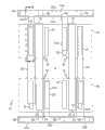
图3为根据本发明的半导体设备的俯视图;3 is a top view of a semiconductor device according to the present invention;
图4为沿着图3所示的线4-4来看的根据本发明的半导体设备的一部分的侧视图;以及FIG. 4 is a side view of a portion of a semiconductor device according to the present invention viewed along line 4-4 shown in FIG. 3; and
图5为根据本发明的半导体设备的金属层的俯视图。5 is a top view of a metal layer of a semiconductor device according to the present invention.
主要组件符号说明Explanation of main component symbols
4-4 线4-4 line
10、100 半导体设备10, 100 Semiconductor equipment
12 半导体基板12 Semiconductor substrate
14、104 扩散区14, 104 Diffusion zone
14a 第一扩散区14a First Diffusion Zone
14b 第二扩散区14b Second Diffusion Zone
16、102 晶体管16, 102 Transistors
18 源极18 source
20 漏极20 Drain
22 栅极22 grid
24 条24 Articles
25 金属层25 metal layer
26、106 电力轨26, 106 power rail
26a 第一电力轨26a First power rail
26b 第二电力轨26b Second power rail
28 接触层28 Contact layer
28a 第一接触层28a First contact layer
28b 第二接触层28b Second contact layer
30、30a、30b 第一长度30, 30a, 30b first length
32、32a、32b 第二长度32, 32a, 32b second length
34 额外长度34 extra length
34a、34b 第三长度34a, 34b third length
36、110 盲孔36, 110 Blind hole
38 接脚层38 pin layer
107 第一金属层107 first metal layer
108 电力突片108 Power tabs
112 电路组件接脚。112 Circuit component pins.
具体实施方式Detailed ways
下列本发明的实施方式本质上仅是例示,且并不是要限制本发明或本发明的应用与使用。再者,并非意欲要被本发明的背景技术或本发明的实施方式中呈现的任何理论所限制。The following embodiments of the invention are merely exemplary in nature and are not intended to limit the invention or the application and uses of the invention. Furthermore, there is no intention to be bound by any theory presented in this background of the invention or the detailed description of the invention.
参照图式,其中,相同的组件符号在所有图式中代表类似的部件,在此显示与描述半导体设备10。该半导体设备10可为集成电路(不分别标号)的部分,且是本领域的技术人员所熟知者。Referring to the drawings, wherein like reference numerals represent like components throughout the several views,
参照图3,该半导体设备10包含半导体基板12。该半导体基板12包含至少一个扩散区14与形成于该至少一个扩散区14中的至少一个晶体管16。在图标的实施例中,第一扩散区14a与第二扩散区14b显示在各区14a、14b中形成有多个晶体管16。然而,本领域的技术人员理解可实施额外的扩散区14a、14b。Referring to FIG. 3 , the
在图标的实施例中,该晶体管16为场效晶体管(FET),更具体来说是金氧半场效晶体管(MOSFET)。各该晶体管16包含源极18、漏极20与栅极22。使用本领域的技术人员所熟知的技术以在该基板12中及/或上形成该源极18、漏极20与栅极22。在图标的实施例中,该栅极22主要由配置在该基板12上方的多晶硅(polycrystalline silicon)(通常称为polysilicon或简称PolySi)形成。In the illustrated embodiment, the
参照图3,该栅极22形成为彼此大致平行的多条(strip)24。该条24大致为如本领域的技术人员所理解的线性形状。可形成间隙(未图标)在该条24中,使得一个以上的晶体管16可沿着各条24设置。此种间隙可使用如本领域的技术人员容易理解的切割屏蔽技术(cut masktechnique)来形成。Referring to FIG. 3 , the
如参照图4所能最佳理解地,该半导体设备10包含设置在该基板12上方的至少一个金属层25。该至少一个金属层25也设置在该晶体管16的源极18、漏极20与栅极22上方。该至少一个金属层25是由铜或如本领域的技术人员所理解的一些其它导电金属所形成。金属层25常规地标示与称为金属1、金属2等或M1、M2等,如本领域的技术人员所理解者。As best understood with reference to FIG. 4 , the
所图标的实施例的金属层25包含至少一个电力轨26。该电力轨26通常如本领域的技术人员所理解的提供参考电压或接地。再次参照图3,该至少一个电力轨26设置在该至少一个扩散区14之外。也就是,该至少一个电力轨26并不重迭该至少一个扩散区14。换句话说,该至少一个电力轨26并不延伸至该至少一个扩散区14中、在该至少一个扩散区14上方或在该至少一个扩散区14下方。在该图标的实施例中,第一电力轨26a是设置在该第一扩散区14a之外而相邻于该第一扩散区14a。同样地,第二电力轨26b是设置在该第二扩散区14b之外而相邻于该第二扩散区14b。Metal layer 25 of the illustrated embodiment includes at least one power rail 26 . The power rail 26 typically provides a reference voltage or ground as understood by those skilled in the art. Referring again to FIG. 3 , the at least one power rail 26 is disposed outside the at least one diffusion region 14 . That is, the at least one power rail 26 does not overlap the at least one diffusion region 14 . In other words, the at least one power rail 26 does not extend into, above or below the at least one diffusion region 14 . In the illustrated embodiment, the
同样在该图标的实施例中,各电力轨26a、26b的至少一区(未标号)是大致线性形状。也就是,各电力轨26a、26b的至少一区纵向延伸,即沿着长度方向。具体而言,各电力轨26a、26b的区是大致线性相邻于个别的扩散区14a、14b。当然,该至少一个电力轨26可包含额外的曲线、弯曲或其它非线性区。Also in the illustrated embodiment, at least one region (not numbered) of each
该半导体设备10进一步包含至少一个接触层(contact layer)28,其用以在该至少一个电力轨26与该至少一个晶体管16之间提供电性连接。该至少一个接触层28由半导体材料(例如硅)形成。然而,该至少一个接触层28可由如本领域的技术人员所理解之能提供导电性的其它半导体材料或其它适当材料形成。该至少一个接触层28设置在该基板12上方及该至少一个电力轨26下方。换句话说,该至少一个接触层28是夹在该基板12与该至少一个电力轨26之间。更具体地说,在图标的实施例中,该至少一个接触层28的至少一部份是直接设置在该基板12上,如图4所示。再次参照图3,该图标的实施例的半导体设备10包含第一接触层28a与第二接触层28b。The
该至少一个接触层28包含至少第一长度30与第二长度32。该至少一个接触层28的第一长度30设置在该至少一个扩散区14之外。也就是,该至少一个接触层28的第一长度30并不重迭该至少一个扩散区14。在图标的实施例中,各接触层28a、28b包含第一长度30a、30b,该第一长度30a、30b延伸大致与各该电力轨26a、26b一致。也就是,各接触层28a、28b的第一长度30a、30b直接设置在各该电力轨26a、26b下方。如此,则各接触层28a、28b的第一长度30a、30b也大致线性形状。此外,在图标的实施例中,各接触层28a、28b的第一长度30a、30b大致垂直于该晶体管16的栅极22。The at least one contact layer 28 includes at least a first length 30 and a second length 32 . A first length 30 of the at least one contact layer 28 is arranged outside the at least one diffusion region 14 . That is, the first length 30 of the at least one contact layer 28 does not overlap the at least one diffusion region 14 . In the illustrated embodiment, each
至少一个盲孔36设置在该至少一个接触层28与该至少一个电力轨26之间。该至少一个盲孔36将该至少一个接触层28电性连接至该至少一个电力轨26。在图标的实施例中,多个盲孔36设置在各电力轨26a、26b与各接触层28a、28b的该第一长度30a、30b之间。该图标的实施例的盲孔36彼此间隔以在该接触层28a、28b与该电力轨26a、26b之间提供平衡的导电性。At least one blind via 36 is disposed between the at least one contact layer 28 and the at least one power rail 26 . The at least one blind via 36 electrically connects the at least one contact layer 28 to the at least one power rail 26 . In the illustrated embodiment, a plurality of
该至少一个接触层28包含从该第一长度30延伸至该至少一个扩散区14中的至少一个额外长度32、34。各额外长度32、34电性连接至至少一个晶体管16。在图标的实施例中,各额外长度32、34电性连接至晶体管的源极18或漏极20。然而,可将至少一个额外长度32、34电性连接至其中一个该晶体管16的栅极22。The at least one contact layer 28 includes at least one additional length 32 , 34 extending from the first length 30 into the at least one diffusion region 14 . Each additional length 32 , 34 is electrically connected to at least one
该图标的实施例的各接触层28a、28b包含第二长度32a、32b与第三长度34a、34b。在图标的实施例中,该接触层28a、28b的第二与第三长度32a、32b、34a、34b也是大致线性形状。此外,该第二与第三长度32a、32b、34a、34b各大致垂直于该接触层28a、28b的各该第一长度30a、30b。如此,则该第二与第三长度32a、32b、34a、34b各大致平行于该晶体管16的栅极22。Each
借由通过该至少一个接触层28将该至少一个晶体管16连接至该至少一个电力轨26,该至少一个电力轨26就不需要突出至该至少一个扩散区14中。如此,则该金属层25可更简单与简洁地使用于该等晶体管16之间的互连,如图5所示。By connecting the at least one
再次参照图3与图4,该半导体设备10的金属层25也可包含位于该至少一个晶体管16上方的接脚层38。如本领域的技术人员所理解者,该接脚层38是互补式金氧半导体(CMOS)电路的标准特征。具体而言,通常使用该接脚层38以将p-沟道晶体管的源极或漏极连接至n沟道晶体管的源极或漏极。如此,则在图标的实施例中,该接脚层38从该扩散区14延伸至该扩散区14之外。更具体来说,该图标的实施例的接脚层38延伸在该第一扩散区14a与该第二扩散区14b之间。Referring again to FIGS. 3 and 4 , the metal layer 25 of the
借由通过该至少一个接触层28将该至少一个晶体管16连接至该至少一个电力轨26,相比于习知技术的设备,由于该金属层25没有从该电力轨26突出至该扩散区14中,所以该接脚层38的尺寸可更大(也就是具有更大的长度、宽度及/或表面积)。这将改善该接脚层38与其它组件(未图标)之间的导电性。By connecting the at least one
虽然本发明的前述详细的实施方式中已经呈现至少一例示实施例,但应该了解存在有很多的变化型式。也应该了解的是,该例示实施例仅是例子,且并非想要以任何方式来限制本发明的范畴、可应用性或组构。倒不如是说,前述实施方式将提供本领域的技术人员实施本发明的例示实施例的方便准则,并了解在不背离如权利要求与其法律等效物的本发明的范畴下,可在例示实施例中所描述的组件的功能与配置上进行各种改变。While at least one illustrative embodiment has been presented in the foregoing detailed description of the invention, it should be appreciated that many variations exist. It should also be understood that the illustrated embodiment is an example only, and is not intended to limit the scope, applicability, or configuration of the invention in any way. Rather, the foregoing embodiments will provide those skilled in the art with a convenient guideline for implementing the exemplary embodiments of the invention, with the understanding that the exemplary embodiments may be implemented without departing from the scope of the invention as claimed and their legal equivalents. Various changes may be made in the functions and configurations of components described in the examples.
Claims (20)
Applications Claiming Priority (2)
| Application Number | Priority Date | Filing Date | Title |
|---|---|---|---|
| US13/351,101US8598633B2 (en) | 2012-01-16 | 2012-01-16 | Semiconductor device having contact layer providing electrical connections |
| US13/351,101 | 2012-01-16 |
Publications (2)
| Publication Number | Publication Date |
|---|---|
| CN103208493Atrue CN103208493A (en) | 2013-07-17 |
| CN103208493B CN103208493B (en) | 2015-09-23 |
Family
ID=48693287
Family Applications (1)
| Application Number | Title | Priority Date | Filing Date |
|---|---|---|---|
| CN201310013910.9AActiveCN103208493B (en) | 2012-01-16 | 2013-01-15 | Semiconductor equipment |
Country Status (6)
| Country | Link |
|---|---|
| US (1) | US8598633B2 (en) |
| KR (1) | KR101616490B1 (en) |
| CN (1) | CN103208493B (en) |
| DE (1) | DE102012215529B4 (en) |
| SG (1) | SG192321A1 (en) |
| TW (1) | TWI499036B (en) |
Cited By (1)
| Publication number | Priority date | Publication date | Assignee | Title |
|---|---|---|---|---|
| CN105845676A (en)* | 2015-01-30 | 2016-08-10 | 台湾积体电路制造股份有限公司 | Semiconductor device and layout method thereof |
Families Citing this family (2)
| Publication number | Priority date | Publication date | Assignee | Title |
|---|---|---|---|---|
| US9496179B2 (en) | 2014-08-25 | 2016-11-15 | Samsung Electronics Co., Ltd. | Method of manufacturing semiconductor devices |
| US10811357B2 (en) | 2017-04-11 | 2020-10-20 | Samsung Electronics Co., Ltd. | Standard cell and an integrated circuit including the same |
Citations (3)
| Publication number | Priority date | Publication date | Assignee | Title |
|---|---|---|---|---|
| CN1747099A (en)* | 2004-09-06 | 2006-03-15 | 沖电气工业株式会社 | Semiconductor device |
| US20060145263A1 (en)* | 2005-01-06 | 2006-07-06 | Macronix International Co., Ltd. | Plasma damage protection circuit for protecting multiple word lines or strapped word lines of a memory device |
| US20080099831A1 (en)* | 2006-10-31 | 2008-05-01 | Oki Electric Industry Co., Ltd. | Semiconductor memory device and method for the same |
Family Cites Families (5)
| Publication number | Priority date | Publication date | Assignee | Title |
|---|---|---|---|---|
| JP2005183681A (en) | 2003-12-19 | 2005-07-07 | Sony Corp | Semiconductor integrated circuit |
| US7763534B2 (en)* | 2007-10-26 | 2010-07-27 | Tela Innovations, Inc. | Methods, structures and designs for self-aligning local interconnects used in integrated circuits |
| JP5130596B2 (en)* | 2007-05-30 | 2013-01-30 | 国立大学法人東北大学 | Semiconductor device |
| US20100052896A1 (en)* | 2008-09-02 | 2010-03-04 | Jesse Bruce Goodman | Fall detection system and method |
| US20110235407A1 (en)* | 2010-03-24 | 2011-09-29 | Sun-Me Lim | Semiconductor memory device and a method of manufacturing the same |
- 2012
- 2012-01-16USUS13/351,101patent/US8598633B2/enactiveActive
- 2012-08-01TWTW101127702Apatent/TWI499036B/enactive
- 2012-08-06SGSG2012058699Apatent/SG192321A1/enunknown
- 2012-08-31DEDE102012215529.5Apatent/DE102012215529B4/enactiveActive
- 2012-09-28KRKR1020120109238Apatent/KR101616490B1/enactiveActive
- 2013
- 2013-01-15CNCN201310013910.9Apatent/CN103208493B/enactiveActive
Patent Citations (3)
| Publication number | Priority date | Publication date | Assignee | Title |
|---|---|---|---|---|
| CN1747099A (en)* | 2004-09-06 | 2006-03-15 | 沖电气工业株式会社 | Semiconductor device |
| US20060145263A1 (en)* | 2005-01-06 | 2006-07-06 | Macronix International Co., Ltd. | Plasma damage protection circuit for protecting multiple word lines or strapped word lines of a memory device |
| US20080099831A1 (en)* | 2006-10-31 | 2008-05-01 | Oki Electric Industry Co., Ltd. | Semiconductor memory device and method for the same |
Cited By (2)
| Publication number | Priority date | Publication date | Assignee | Title |
|---|---|---|---|---|
| CN105845676A (en)* | 2015-01-30 | 2016-08-10 | 台湾积体电路制造股份有限公司 | Semiconductor device and layout method thereof |
| CN105845676B (en)* | 2015-01-30 | 2019-11-01 | 台湾积体电路制造股份有限公司 | Semiconductor devices and its layout method |
Also Published As
| Publication number | Publication date |
|---|---|
| KR101616490B1 (en) | 2016-04-28 |
| KR20130084205A (en) | 2013-07-24 |
| US8598633B2 (en) | 2013-12-03 |
| DE102012215529A1 (en) | 2013-07-18 |
| US20130181289A1 (en) | 2013-07-18 |
| DE102012215529B4 (en) | 2018-07-12 |
| CN103208493B (en) | 2015-09-23 |
| TWI499036B (en) | 2015-09-01 |
| SG192321A1 (en) | 2013-08-30 |
| TW201332086A (en) | 2013-08-01 |
Similar Documents
| Publication | Publication Date | Title |
|---|---|---|
| TWI574411B (en) | Semiconductor device with transistor region interconnection | |
| CN103165575B (en) | There is the semiconductor equipment of transistor area interconnection | |
| CN104425443B (en) | The semiconductor logic circuit manufactured using multilayered structure | |
| TWI630720B (en) | Semiconductor device | |
| TW201017451A (en) | Semiconductor integrated circuit device and a method of manufacturing the same | |
| CN108074920B (en) | semiconductor device | |
| CN102420145B (en) | The implementation method of series connection FinFET | |
| CN103208493B (en) | Semiconductor equipment | |
| US9450089B2 (en) | Semiconductor device | |
| CN108666296A (en) | transistor structure | |
| JP2009016725A (en) | Semiconductor device | |
| JP2009158728A (en) | Semiconductor device | |
| CN104919577A (en) | Semiconductor device |
Legal Events
| Date | Code | Title | Description |
|---|---|---|---|
| C06 | Publication | ||
| PB01 | Publication | ||
| C10 | Entry into substantive examination | ||
| SE01 | Entry into force of request for substantive examination | ||
| C14 | Grant of patent or utility model | ||
| GR01 | Patent grant |