CN103187510A - Solid-state light-emitting element and solid-state light-emitting package thereof - Google Patents
Solid-state light-emitting element and solid-state light-emitting package thereofDownload PDFInfo
- Publication number
- CN103187510A CN103187510ACN2012102132275ACN201210213227ACN103187510ACN 103187510 ACN103187510 ACN 103187510ACN 2012102132275 ACN2012102132275 ACN 2012102132275ACN 201210213227 ACN201210213227 ACN 201210213227ACN 103187510 ACN103187510 ACN 103187510A
- Authority
- CN
- China
- Prior art keywords
- solid
- state light
- electrode piece
- emitting
- packaging body
- Prior art date
- Legal status (The legal status is an assumption and is not a legal conclusion. Google has not performed a legal analysis and makes no representation as to the accuracy of the status listed.)
- Pending
Links
Images


Classifications
- H—ELECTRICITY
- H01—ELECTRIC ELEMENTS
- H01L—SEMICONDUCTOR DEVICES NOT COVERED BY CLASS H10
- H01L24/00—Arrangements for connecting or disconnecting semiconductor or solid-state bodies; Methods or apparatus related thereto
- H01L24/93—Batch processes
- H01L24/95—Batch processes at chip-level, i.e. with connecting carried out on a plurality of singulated devices, i.e. on diced chips
- H01L24/97—Batch processes at chip-level, i.e. with connecting carried out on a plurality of singulated devices, i.e. on diced chips the devices being connected to a common substrate, e.g. interposer, said common substrate being separable into individual assemblies after connecting
- H—ELECTRICITY
- H10—SEMICONDUCTOR DEVICES; ELECTRIC SOLID-STATE DEVICES NOT OTHERWISE PROVIDED FOR
- H10H—INORGANIC LIGHT-EMITTING SEMICONDUCTOR DEVICES HAVING POTENTIAL BARRIERS
- H10H20/00—Individual inorganic light-emitting semiconductor devices having potential barriers, e.g. light-emitting diodes [LED]
- H10H20/80—Constructional details
- H10H20/85—Packages
- H10H20/857—Interconnections, e.g. lead-frames, bond wires or solder balls
- H—ELECTRICITY
- H01—ELECTRIC ELEMENTS
- H01L—SEMICONDUCTOR DEVICES NOT COVERED BY CLASS H10
- H01L2224/00—Indexing scheme for arrangements for connecting or disconnecting semiconductor or solid-state bodies and methods related thereto as covered by H01L24/00
- H01L2224/01—Means for bonding being attached to, or being formed on, the surface to be connected, e.g. chip-to-package, die-attach, "first-level" interconnects; Manufacturing methods related thereto
- H01L2224/10—Bump connectors; Manufacturing methods related thereto
- H01L2224/15—Structure, shape, material or disposition of the bump connectors after the connecting process
- H01L2224/16—Structure, shape, material or disposition of the bump connectors after the connecting process of an individual bump connector
- H01L2224/161—Disposition
- H01L2224/16151—Disposition the bump connector connecting between a semiconductor or solid-state body and an item not being a semiconductor or solid-state body, e.g. chip-to-substrate, chip-to-passive
- H01L2224/16221—Disposition the bump connector connecting between a semiconductor or solid-state body and an item not being a semiconductor or solid-state body, e.g. chip-to-substrate, chip-to-passive the body and the item being stacked
- H01L2224/16245—Disposition the bump connector connecting between a semiconductor or solid-state body and an item not being a semiconductor or solid-state body, e.g. chip-to-substrate, chip-to-passive the body and the item being stacked the item being metallic
- H—ELECTRICITY
- H01—ELECTRIC ELEMENTS
- H01L—SEMICONDUCTOR DEVICES NOT COVERED BY CLASS H10
- H01L2224/00—Indexing scheme for arrangements for connecting or disconnecting semiconductor or solid-state bodies and methods related thereto as covered by H01L24/00
- H01L2224/01—Means for bonding being attached to, or being formed on, the surface to be connected, e.g. chip-to-package, die-attach, "first-level" interconnects; Manufacturing methods related thereto
- H01L2224/42—Wire connectors; Manufacturing methods related thereto
- H01L2224/47—Structure, shape, material or disposition of the wire connectors after the connecting process
- H01L2224/48—Structure, shape, material or disposition of the wire connectors after the connecting process of an individual wire connector
- H01L2224/4805—Shape
- H01L2224/4809—Loop shape
- H01L2224/48091—Arched
- H—ELECTRICITY
- H01—ELECTRIC ELEMENTS
- H01L—SEMICONDUCTOR DEVICES NOT COVERED BY CLASS H10
- H01L2224/00—Indexing scheme for arrangements for connecting or disconnecting semiconductor or solid-state bodies and methods related thereto as covered by H01L24/00
- H01L2224/01—Means for bonding being attached to, or being formed on, the surface to be connected, e.g. chip-to-package, die-attach, "first-level" interconnects; Manufacturing methods related thereto
- H01L2224/42—Wire connectors; Manufacturing methods related thereto
- H01L2224/47—Structure, shape, material or disposition of the wire connectors after the connecting process
- H01L2224/48—Structure, shape, material or disposition of the wire connectors after the connecting process of an individual wire connector
- H01L2224/481—Disposition
- H01L2224/48151—Connecting between a semiconductor or solid-state body and an item not being a semiconductor or solid-state body, e.g. chip-to-substrate, chip-to-passive
- H01L2224/48221—Connecting between a semiconductor or solid-state body and an item not being a semiconductor or solid-state body, e.g. chip-to-substrate, chip-to-passive the body and the item being stacked
- H01L2224/48245—Connecting between a semiconductor or solid-state body and an item not being a semiconductor or solid-state body, e.g. chip-to-substrate, chip-to-passive the body and the item being stacked the item being metallic
- H01L2224/48247—Connecting between a semiconductor or solid-state body and an item not being a semiconductor or solid-state body, e.g. chip-to-substrate, chip-to-passive the body and the item being stacked the item being metallic connecting the wire to a bond pad of the item
- H—ELECTRICITY
- H01—ELECTRIC ELEMENTS
- H01L—SEMICONDUCTOR DEVICES NOT COVERED BY CLASS H10
- H01L25/00—Assemblies consisting of a plurality of semiconductor or other solid state devices
- H01L25/03—Assemblies consisting of a plurality of semiconductor or other solid state devices all the devices being of a type provided for in a single subclass of subclasses H10B, H10D, H10F, H10H, H10K or H10N, e.g. assemblies of rectifier diodes
- H01L25/04—Assemblies consisting of a plurality of semiconductor or other solid state devices all the devices being of a type provided for in a single subclass of subclasses H10B, H10D, H10F, H10H, H10K or H10N, e.g. assemblies of rectifier diodes the devices not having separate containers
- H01L25/075—Assemblies consisting of a plurality of semiconductor or other solid state devices all the devices being of a type provided for in a single subclass of subclasses H10B, H10D, H10F, H10H, H10K or H10N, e.g. assemblies of rectifier diodes the devices not having separate containers the devices being of a type provided for in group H10H20/00
- H01L25/0753—Assemblies consisting of a plurality of semiconductor or other solid state devices all the devices being of a type provided for in a single subclass of subclasses H10B, H10D, H10F, H10H, H10K or H10N, e.g. assemblies of rectifier diodes the devices not having separate containers the devices being of a type provided for in group H10H20/00 the devices being arranged next to each other
- H—ELECTRICITY
- H01—ELECTRIC ELEMENTS
- H01L—SEMICONDUCTOR DEVICES NOT COVERED BY CLASS H10
- H01L2924/00—Indexing scheme for arrangements or methods for connecting or disconnecting semiconductor or solid-state bodies as covered by H01L24/00
- H01L2924/10—Details of semiconductor or other solid state devices to be connected
- H01L2924/11—Device type
- H01L2924/12—Passive devices, e.g. 2 terminal devices
- H01L2924/1204—Optical Diode
- H01L2924/12041—LED
- H—ELECTRICITY
- H01—ELECTRIC ELEMENTS
- H01L—SEMICONDUCTOR DEVICES NOT COVERED BY CLASS H10
- H01L2924/00—Indexing scheme for arrangements or methods for connecting or disconnecting semiconductor or solid-state bodies as covered by H01L24/00
- H01L2924/15—Details of package parts other than the semiconductor or other solid state devices to be connected
- H01L2924/181—Encapsulation
- H—ELECTRICITY
- H10—SEMICONDUCTOR DEVICES; ELECTRIC SOLID-STATE DEVICES NOT OTHERWISE PROVIDED FOR
- H10H—INORGANIC LIGHT-EMITTING SEMICONDUCTOR DEVICES HAVING POTENTIAL BARRIERS
- H10H20/00—Individual inorganic light-emitting semiconductor devices having potential barriers, e.g. light-emitting diodes [LED]
- H10H20/01—Manufacture or treatment
- H10H20/036—Manufacture or treatment of packages
- H10H20/0364—Manufacture or treatment of packages of interconnections
- H—ELECTRICITY
- H10—SEMICONDUCTOR DEVICES; ELECTRIC SOLID-STATE DEVICES NOT OTHERWISE PROVIDED FOR
- H10H—INORGANIC LIGHT-EMITTING SEMICONDUCTOR DEVICES HAVING POTENTIAL BARRIERS
- H10H20/00—Individual inorganic light-emitting semiconductor devices having potential barriers, e.g. light-emitting diodes [LED]
- H10H20/80—Constructional details
- H10H20/85—Packages
- H10H20/8506—Containers
- H—ELECTRICITY
- H10—SEMICONDUCTOR DEVICES; ELECTRIC SOLID-STATE DEVICES NOT OTHERWISE PROVIDED FOR
- H10H—INORGANIC LIGHT-EMITTING SEMICONDUCTOR DEVICES HAVING POTENTIAL BARRIERS
- H10H20/00—Individual inorganic light-emitting semiconductor devices having potential barriers, e.g. light-emitting diodes [LED]
- H10H20/80—Constructional details
- H10H20/85—Packages
- H10H20/852—Encapsulations
- H—ELECTRICITY
- H10—SEMICONDUCTOR DEVICES; ELECTRIC SOLID-STATE DEVICES NOT OTHERWISE PROVIDED FOR
- H10H—INORGANIC LIGHT-EMITTING SEMICONDUCTOR DEVICES HAVING POTENTIAL BARRIERS
- H10H20/00—Individual inorganic light-emitting semiconductor devices having potential barriers, e.g. light-emitting diodes [LED]
- H10H20/80—Constructional details
- H10H20/85—Packages
- H10H20/858—Means for heat extraction or cooling
Landscapes
- Engineering & Computer Science (AREA)
- Computer Hardware Design (AREA)
- Microelectronics & Electronic Packaging (AREA)
- Power Engineering (AREA)
- Led Device Packages (AREA)
Abstract
Translated fromChineseDescription
Translated fromChinese技术领域technical field
本发明涉及一种发光装置,且特别涉及一种固态发光元件及其固态发光封装体。The invention relates to a light-emitting device, and in particular to a solid-state light-emitting element and a solid-state light-emitting package.
背景技术Background technique
在现有发光二极管(Light Emitting Diode,LED)的封装技术中,目前已发展出一种塑料引线芯片载体类型(Plastic Leaded Chip Carrier Type,PLCC Type)的封装结构,而具有这种封装结构的发光二极管封装体不仅包括导线架(lead frame)、发光二极管芯片(LED Chip)以及封装胶体,而且还包括一塑料碗杯。In the existing packaging technology of Light Emitting Diode (LED), a packaging structure of Plastic Leaded Chip Carrier Type (PLCC Type) has been developed, and the light emitting diode with this packaging structure The diode package includes not only lead frame, LED Chip and encapsulant, but also a plastic bowl.
在这种发光二极管封装体中,导线架与塑料碗杯结合,而发光二极管芯片装设(mounted)在导线架上,并且位于塑料碗杯的碗底。封装胶体会填满塑料碗杯,并且包覆发光二极管芯片及导线架。塑料碗杯是在导线架完成之后,利用模具成型的方法,例如射出成型,而形成。In this LED package, the lead frame is combined with the plastic bowl, and the LED chip is mounted on the lead frame and located at the bottom of the plastic bowl. The encapsulant will fill the plastic bowl and cover the LED chip and the lead frame. The plastic cup is formed by mold molding, such as injection molding, after the lead frame is completed.
因此,在上述发光二极管封装体的制造流程中,塑料碗杯的模具必须事先完成,才能形成与导线架结合的塑料碗杯。然而,上述模具的开发与制作需要耗费相当的时间与金钱,因而增加发光二极管封装体的制造成本。Therefore, in the above-mentioned manufacturing process of the light emitting diode package, the mold of the plastic bowl must be completed in advance to form the plastic bowl combined with the lead frame. However, the development and manufacture of the above-mentioned molds consume considerable time and money, thus increasing the manufacturing cost of the LED package.
发明内容Contents of the invention
本发明的目的在于提供一种固态发光封装体,其不包括上述塑料碗杯,以降低因塑料碗杯的模具开发及制作所产生的制造成本。The object of the present invention is to provide a solid-state light emitting package, which does not include the above-mentioned plastic cup, so as to reduce the manufacturing cost caused by mold development and production of the plastic cup.
本发明提供一种固态发光元件,其包括多个上述固态发光封装体。The present invention provides a solid-state light-emitting element, which includes a plurality of above-mentioned solid-state light-emitting packages.
本发明提出一种固态发光封装体,其包括一导线架、一发光芯片以及一封装胶体。导线架包括一第一电极件与一第二电极件。第一电极件具有至少一第一接触端,而第二电极件具有至少一第二接触端。发光芯片电性连接第一电极件与第二电极件,并位在第一接触端与第二接触端之间,其中发光芯片用于发出一光线。封装胶体包覆导线架与发光芯片。封装胶体具有相对的一第一表面与一第二表面,其中第一表面为发光芯片的出光面。第一电极件与第二电极件皆朝向第一表面而弯曲,而第一表面暴露第一接触端与第二接触端的顶部区域。The invention provides a solid-state light-emitting package, which includes a lead frame, a light-emitting chip, and a packaging colloid. The lead frame includes a first pole piece and a second pole piece. The first electrode part has at least one first contact end, and the second electrode part has at least one second contact end. The light-emitting chip is electrically connected to the first electrode member and the second electrode member, and is located between the first contact end and the second contact end, wherein the light-emitting chip is used for emitting a light. The encapsulation colloid covers the lead frame and the light-emitting chip. The packaging colloid has a first surface and a second surface opposite to each other, wherein the first surface is the light-emitting surface of the light-emitting chip. Both the first electrode member and the second electrode member are bent toward the first surface, and the first surface exposes top regions of the first contact end and the second contact end.
本发明另提出一种固态发光元件,其包括多个上述固态发光封装体。The present invention further provides a solid-state light-emitting device, which includes a plurality of the above-mentioned solid-state light-emitting packages.
基于上述,本发明的固态发光元件及固态发光封装体是采用封装胶体与导线架来封装发光芯片,不采用现有的塑料碗杯。因此,本发明的固态发光元件及固态发光封装体能降低因塑料碗杯的模具开发及制作所产生的制造成本。Based on the above, the solid-state light-emitting device and the solid-state light-emitting package of the present invention use packaging colloid and a lead frame to package the light-emitting chip, instead of using the existing plastic cup. Therefore, the solid-state light-emitting device and the solid-state light-emitting package of the present invention can reduce the manufacturing cost caused by mold development and production of plastic bowls and cups.
为使能更进一步了解本发明的特征及技术内容,请参阅以下有关本发明的详细说明及附图,但是此等说明与附图仅用来说明本发明,而非对本发明的权利范围作任何的限制。In order to enable a further understanding of the features and technical content of the present invention, please refer to the following detailed descriptions and drawings of the present invention, but these descriptions and drawings are only used to illustrate the present invention, rather than to make any statement on the scope of rights of the present invention. limits.
附图说明Description of drawings
图1A是本发明一实施例的固态发光封装体的立体示意图。FIG. 1A is a schematic perspective view of a solid-state light emitting package according to an embodiment of the present invention.
图1B是图1A中固态发光封装体的侧视示意图。FIG. 1B is a schematic side view of the solid-state light emitting package in FIG. 1A .
图2A是本发明另一实施例的固态发光封装体的立体示意图。FIG. 2A is a schematic perspective view of a solid-state light emitting package according to another embodiment of the present invention.
图2B是图2A中固态发光封装体的侧视示意图。FIG. 2B is a schematic side view of the solid-state light emitting package in FIG. 2A .
图3A是本发明另一实施例的固态发光封装体的立体示意图。FIG. 3A is a schematic perspective view of a solid-state light emitting package according to another embodiment of the present invention.
图3B是图3A中固态发光封装体的侧视示意图。FIG. 3B is a schematic side view of the solid-state light emitting package in FIG. 3A .
图4A是本发明一实施例的固态发光元件的立体示意图。FIG. 4A is a three-dimensional schematic diagram of a solid-state light emitting device according to an embodiment of the present invention.
图4B是图4A中区域A的放大示意图。FIG. 4B is an enlarged schematic view of area A in FIG. 4A .
图5是本发明另一实施例的固态发光元件的立体示意图。FIG. 5 is a schematic perspective view of a solid-state light emitting device according to another embodiment of the present invention.
其中,附图标记说明如下:Wherein, the reference signs are explained as follows:
100、200、300:固态发光封装体100, 200, 300: solid state light emitting package
110、210、310:导线架110, 210, 310: lead frame
111、211:第一电极件111, 211: the first electrode piece
111a、211a:第一接触端111a, 211a: first contact end
112a、212a:第二接触端112a, 212a: second contact end
112、212:第二电极件112, 212: second pole piece
120、220:发光芯片120, 220: light-emitting chip
122、222:发光面122, 222: light emitting surface
124、224、B11、B12、B21、B22、B23:底面124, 224, B11, B12, B21, B22, B23: Bottom
130:封装胶体130: encapsulation colloid
131:第一表面131: First Surface
132:第二表面132: second surface
133:第三表面133: Third Surface
134:第四表面134: The fourth surface
140:焊料凸块140: Solder bumps
213:承载件213: Carrier
213a、T13、T14、S21、S22:侧边区域213a, T13, T14, S21, S22: side area
240:键合导线240: Bonding wire
400、500:固态发光元件400, 500: solid-state light-emitting components
D1:行方向D1: row direction
D2:列方向D2: column direction
E11:第一延伸部E11: first extension
E12:第二延伸部E12: Second extension
L1、L2:光线L1, L2: light
G1、G2、G3:间隔G1, G2, G3: Interval
S11:第一承载部S11: the first bearing part
S12:第二承载部S12: the second carrying part
T11、T12、T21、T22:顶部区域T11, T12, T21, T22: top area
具体实施方式Detailed ways
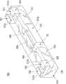
图1A是本发明一实施例的固态发光封装体的立体示意图,而图1B是图1A中固态发光封装体的侧视示意图。请参阅图1A与图1B,固态发光封装体100包括一导线架110、一发光芯片120以及一封装胶体130,其中发光芯片120装设在导线架110上,并且电性连接导线架110,而封装胶体130包覆导线架110与发光芯片120。FIG. 1A is a schematic perspective view of a solid state light emitting package according to an embodiment of the present invention, and FIG. 1B is a schematic side view of the solid state light emitting package in FIG. 1A . Referring to FIG. 1A and FIG. 1B, the solid-state
导线架110是由金属材料所制成,并且包括一第一电极件111与一第二电极件112,其中第一电极件111具有至少一第一接触端111a,而第二电极件112具有至少一第二接触端112a。以图1A所示的实施例为例,第一电极件111所具有的第一接触端111a的数量为两个,而第二电极件112所具有的第二接触端112a的数量也为两个。The
然而,在其它实施例中,第一电极件111所具有的第一接触端111a的数量可以仅为一个或是两个以上,而第二电极件112所具有的第二接触端112a的数量也可以仅为一个或是两个以上,因此图1A中的第一接触端111a与第二接触端112a二者的数量仅供举例说明,并非限定本发明。However, in other embodiments, the
封装胶体130具有一第一表面131、一第二表面132、一第三表面133与一第四表面134,其中第一表面131相对于第二表面132,而第三表面133相对于第四表面134。此外,第三表面133与第四表面134连接在第一表面131与第二表面132之间,其中第三表面133相连于第一表面131与第二表面132,而第四表面134也相连于第一表面131与第二表面132。The
封装胶体130局部暴露导线架110。详细而言,第一表面131暴露第一接触端111a与第二接触端112a的顶部区域T11与T12,第二表面132暴露第一电极件111与第二电极件112的底面B11与B12,第三表面133与第四表面134皆暴露第一接触端111a与第二接触端112a的侧边区域T13与T14,如图1A与图1B所示。The
封装胶体130暴露第一接触端111a与第二接触端112a的顶部区域T11与T12,可助于散热。第一电极件111与第二电极件112所暴露的底面B11与B12是用以连接焊料(solder,未绘示),其中焊料例如是焊锡,如此,外部电源可经由焊料、第一电极件111以及第二电极件112而输入电流至导线架110。The
此外,第三表面133与第四表面134暴露第一接触端111a与第二接触端112a的侧边区域T13与T14,可经由侧边区域T13与T14连接焊料(solder,未绘示),其中焊料例如是焊锡。如此,外部电源可经由焊料、第一接触端111a以及第二接触端112a而输入电流至导线架110。故通过暴露的侧边区域T13与T14,可使固态发光封装体100是一种侧光式封装结构,进而应用于侧边入光型的发光装置,例如侧边入光式背光模块、板灯等。In addition, the
在本实施例中,封装胶体130同时暴露电极件的底面B11、B12与接触端的侧边区域T13与T14,但未必要同时暴露,即可根据需求,制作时只暴露电极件的底面B11、B12,或制作时只暴露侧边区域T13与T14。In this embodiment, the
另外,第一电极件111与第二电极件112二者皆具有弯曲的结构,且第一电极件111与第二电极件112皆朝向第一表面131而弯曲。详细而言,第一电极件111包括一第一承载部S11与一连接第一承载部S11的第一延伸部E11,而第二电极件112包括一第二承载部S12与一连接第二承载部S12的第二延伸部E12。In addition, both the
第一延伸部E11从第一承载部S11朝向第一表面131弯曲而延伸至第一接触端111a,而第二延伸部E12从第二承载部S12朝向第一表面131弯曲而延伸至第二接触端112a。如此,第一电极件111与第二电极件112皆具有朝向第一表面131而弯曲的结构。此外,第一电极件111与第二电极件112的弯曲处的外侧为圆弧角状,如图1B所示。The first extension part E11 bends from the first bearing part S11 toward the
发光芯片120电性连接第一电极件111与第二电极件112,并位于第一接触端111a与第二接触端112a之间,其中发光芯片120可以是以覆晶接合(flip chip)方式位于导线架110的第一承载部S11与第二承载部S12上。详细而言,固态发光封装体100可更包括两个焊料凸块140,而这些焊料凸块140位于导线架110与发光芯片120之间,其中发光芯片120可通过这些焊料凸块140分别连接第一承载部S11与第二承载部S12。如此,发光芯片120得以电性连接第一电极件111与第二电极件112。The light-emitting
发光芯片120例如是发光二极管芯片,并且可为正向发光型或侧向发光型的发光二极管芯片。发光芯片120用于发出一光线L1,并且具有一发光面122以及一相对发光面122的底面124,其中这些焊料凸块140皆连接于底面124。The light-emitting
当外部电源经由焊料、第一接触端111a与第二接触端112a而输入电流至导线架110时,电流能从焊料凸块140传递至发光芯片120。如此,发光芯片120能接受电流而从发光面122发出光线L1。此外,光线L1会从第一表面131射出,所以第一表面131可为发光芯片120的出光面。When an external power source inputs current to the
另外,第一承载部S11与第二承载部S12之间存有一间隔G1(space),以至于第一电极件111与第二电极件112彼此不接触,而在固态发光封装体100正常运行的情况下,第一电极件111与第二电极件112二者仅只透过发光芯片120而彼此电性连接。换句话说,如果将图1A与图1B中的发光芯片120移除,则第一电极件111与第二电极件112二者会彼此电性绝缘。In addition, there is a gap G1 (space) between the first bearing part S11 and the second bearing part S12, so that the
图2A是本发明另一实施例的固态发光封装体的立体示意图,而图2B是图2A中固态发光封装体的侧视示意图。请参阅图2A与图2B,固态发光封装体200包括一导线架210、一发光芯片220以及一封装胶体130,其中发光芯片220也可以是发光二极管芯片,其例如是正向发光型或侧向发光型的发光二极管芯片,而固态发光封装体200、100二者结构相似。FIG. 2A is a schematic perspective view of a solid state light emitting package according to another embodiment of the present invention, and FIG. 2B is a schematic side view of the solid state light emitting package in FIG. 2A . Please refer to FIG. 2A and FIG. 2B, the solid state light emitting
举例而言,发光芯片220装设在导线架210上,且封装胶体130包覆发光芯片220与导线架210,并局部暴露导线架210,例如封装胶体130的第一表面131暴露第一接触端211a的顶部区域T21与第二接触端212a的顶部区域T22,而封装胶体130的第二表面132暴露第一电极件211的底面B21与第二电极件212的底面B22。For example, the light-emitting
此外,相同于前述实施例中的第一电极件111与第二电极件112,第一电极件211与第二电极件212二者皆具有弯曲的结构,其中第一电极件211与第二电极件212皆朝向第一表面131而弯曲,如图2A与图2B所示。另外,第一接触端211a与第二接触端212a二者功能相同于第一接触端111a与第二接触端112a,故不再重复赘述。In addition, similar to the
然而,固态发光封装体200、100二者之间仍存有差异,其在于:发光芯片220是以打线接合(wire bonding)方式装设在导线架210上,且导线架210不仅包括第一电极件211与第二电极件212,还包括一承载件213,其中发光芯片220装设在承载件213上,例如发光芯片220可以是利用胶材(adhesive,未绘示)黏合在承载件213上。However, there are still differences between the solid-state light-emitting
具体而言,固态发光封装体200更包括多条键合导线240,其中封装胶体130更包覆这些键合导线240,而各条键合导线240电性连接第一电极件211与第二电极件212二者其中之一以及发光芯片220。因此,发光芯片220能经由这些键合导线240而电性连接第一电极件211与第二电极件212。如此,发光芯片220能经由这些键合导线240、第一电极件211与第二电极件212而接收从外部电源而来的电流,以使发光芯片220得以发出光线L2。Specifically, the solid-state
此外,发光芯片220具有一发光面222以及一相对发光面222的底面224,其中发光芯片220是从发光面222发出光线L2,而底面224连接承载件213,并可利用胶材来连接承载件213。In addition, the light-emitting
承载件213可以配置在第一电极件211与第二电极件212之间,且承载件213与第一电极件211、第二电极件212之间各别存有一间隔G2,即承载件213与第一电极件211隔着一个间隔G2,而承载件213与第二电极件212隔着另一个间隔G2。因此,承载件213、第一电极件211与第二电极件212三者彼此分离。此外,承载件213具有一底面B23,而第二表面132暴露底面B23,如图2B所示。底面B21、B22、B23可连接焊料(solder,未绘示),其中焊料例如是焊锡。The
由于承载件213、第一电极件211与第二电极件212三者彼此分离,因此当发光芯片220发光时,发光芯片220会从第一电极件211与第二电极件212来接收电流,而发光芯片220所产生的热能大部分则从承载件213传递,所以在固态发光封装体200中,电流传递路径与大部分热能的传导路径二者并不相同。Since the
值得一提的是,有别于图1A与图1B,在图2A与图2B的实施例中,封装胶体130的第三表面133与第四表面134并未暴露第一接触端211a的侧边区域S21与第二接触端212a的侧边区域S22。然而,在其它实施例中,封装胶体130的第三表面133与第四表面134也可以如同图1A与图1B所示,局部暴露第一接触端111a的侧边区域T13与第二接触端112a的侧边区域T14。再者,封装胶体130的第三表面133与第四表面134也可以暴露中间承载件213的侧边区域,作为连接焊料用。因此,图2A与图2B所示的固态发光封装体200并不限定本发明。It is worth mentioning that, different from FIG. 1A and FIG. 1B , in the embodiment of FIG. 2A and FIG. 2B , the
图3A是本发明另一实施例的固态发光封装体的立体示意图,而图3B是图3A中固态发光封装体的侧视示意图。请参阅图3A与图3B,本实施例的固态发光封装体300与前述实施例的固态发光封装体200相似,而二者差异包括:固态发光封装体300所包括的导线架310。FIG. 3A is a schematic perspective view of a solid state light emitting package according to another embodiment of the present invention, and FIG. 3B is a schematic side view of the solid state light emitting package in FIG. 3A . Please refer to FIG. 3A and FIG. 3B , the solid state light emitting
具体而言,在导线架310中,承载件213与第一电极件211相连,而承载件213仅与第二电极件212分离,并且与第二电极件212之间存有一间隔G2。换句话说,相较于前述实施例的固态发光封装体200,本实施例的固态发光封装体300仅只具有一个间隔G2。Specifically, in the
由于承载件213与第一电极件211相连,所以在本实施例中,发光芯片220不仅从第一电极件211来接收电流,而且发光芯片220所产生的热能大部分也从承载件213与第一电极件211传递。因此,在固态发光封装体300中,电流传递路径与大部分热能的传导路径会有部分重叠。此外,本实施例的固态发光封装体300与前述实施例的固态发光封装体200二者整体功能都相同,故不再重复赘述。Since the
此外,与图1A中的固态发光封装体100相似,但却不同于图2A与图2B中的固态发光封装体200的地方在于:在图3A与图3B所示的固态发光封装体300中,封装胶体130会暴露第一接触端211a的顶部区域T21与侧边区域S21,以及第二接触端212a的顶部区域T22与侧边区域S22。另外,封装胶体130可以更暴露承载件213的侧边区域213a,如图3A所示。In addition, similar to the solid state light emitting
这些暴露出来的侧边区域S21、S22、承载件213的侧边区域213a可以连接焊料,例如焊锡。如此,外部电源可经由焊料、第一接触端211a以及第二接触端212a而输入电流至导线架310,从而让发光芯片220发光。此外,裸露的顶部区域T21、T22更可以帮助散热,以减少发光芯片220发生过热(overheat)的情形。These exposed side regions S21 , S22 and the
再者,封装胶体130亦可更暴露第一电极件211、第二电极件212、承载件213的底面,以与焊料连接。Moreover, the
须说明的是,在其它实施例中,可根据需求,制作时只暴露侧边区域S21、S22与侧边区域213a,或是制作时只暴露侧边区域S21、S22。因此,图3A与图3B所示的第一接触端211a与第二接触端212a二者裸露的部分仅供举例说明,并非限定本发明。It should be noted that in other embodiments, only the side regions S21 , S22 and the
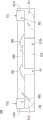
图4A是本发明一实施例的固态发光元件的立体示意图,而图4B是图4A中区域A的放大示意图。请参阅图4A,本实施例的固态发光元件400包括多个前述实施例所揭露的固态发光封装体,而在图4A与图4B所示的实施例中,固态发光元件400所包括的固态发光封装体是以固态发光封装体300(请参阅图3A与图3B)为例。FIG. 4A is a schematic perspective view of a solid-state light emitting device according to an embodiment of the present invention, and FIG. 4B is an enlarged schematic view of area A in FIG. 4A . Please refer to FIG. 4A, the solid-state light-emitting
然而,在其它实施例中,固态发光元件400所包括的固态发光封装体不仅可以是固态发光封装体300,而且也可以是固态发光封装体100(请参阅图1A与图1B)或200(请参阅图2A与图2B)。其次,固态发光元件400不仅可包括单一种固态发光封装体,而且也可包括多种固态发光封装体。例如固态发光元件400可以包括多个固态发光封装体200与300。因此,在此强调,图4A与图4B所示的固态发光封装体的种类仅供举例说明,并非限定本发明。However, in other embodiments, the solid-state light-emitting package included in the solid-state light-emitting
在图4A与图4B所示的实施例中,这些固态发光封装体300可以呈行列排列,其中排列在同一行的这些固态发光封装体300,也就是沿着行方向D1排列的固态发光封装体300,彼此邻接,而每一相邻这些固态发光封装体300行间存有一间隔G3,即沿着列方向D2排列的这些固态发光封装体300彼此之间存有间隔G3。In the embodiment shown in FIG. 4A and FIG. 4B , these solid-state light-emitting
在固态发光元件400中,所有固态发光封装体300的导线架310可以是由至少一块金属板所制造而成,而制造这些导线架310的方法例如是对上述金属板进行机械加工,例如冲床(Stamping Press),以使金属板弯曲并形成这些间隔G2与G3,从而形成部分彼此邻接的导线架310,如图4A与图4B所示。In the solid-state light-emitting
当形成这些导线架310之后,在这些导线架310上装设发光芯片220,其中发光芯片220可以是用覆晶接合或打线接合的方式装设在导线架310上。之后,形成封装胶体130,以将这些导线架310与这些发光芯片220包覆,从而完成固态发光元件400。After the lead frames 310 are formed, the
承上述,当固态发光元件400之后,可以对固态发光元件400进行切割(dicing),以使这些固态发光封装体300彼此分离。换句话说,图3A与图3B所示的固态发光封装体300可从固态发光元件400切割而成,即固态发光封装体300可以是从固态发光元件400所切割下来的一部分。Based on the above, when the solid state light emitting
由于在其它实施例中,固态发光元件400也可以包括多个固态发光封装体100或200,因此图1A、图1B、图2A以及图1B所示的固态发光封装体100与200也可以是从固态发光元件400切割而成,即固态发光封装体100与200也可以是从固态发光元件400所切割下来的一部分。Since in other embodiments, the solid-state
此外,固态发光元件400可以直接作为发光源来使用。例如,固态发光元件400可以用来作为照明灯具的灯源,或是与扩散片(diffuser)及增亮膜(bright enhancement film)等光学膜片(optical film)结合而制作成液晶显示器(Liquid Crystal Display,LCD)的直下入式背光模块(direct-type backlightmodule)。In addition, the solid state
图5是本发明另一实施例的固态发光元件的立体示意图。请参阅图5,本实施例的固态发光元件500与前述固态发光元件400相似,然而差异仅在于:在固态发光元件500中,所有固态发光封装体300是排列成一列,且每一相邻这些导线架310之间存有一间隔G3。FIG. 5 is a schematic perspective view of a solid-state light emitting device according to another embodiment of the present invention. Please refer to Fig. 5, the solid-state light-emitting element 500 of this embodiment is similar to the aforementioned solid-state light-emitting
详细而言,在固态发光元件500中,所有固态发光封装体300是沿着列方向D2排列,且这些固态发光封装体300彼此之间存有间隔G3。此外,固态发光元件500也可以是从固态发光元件400切割而成。换句话说,固态发光元件500可以是从固态发光元件400所切割下来的一部分。In detail, in the solid state light emitting device 500 , all the solid state
此外,固态发光元件500可以作为灯条(light bar)来使用,例如固态发光元件500可以用来作为照明灯具的灯源,或是与导光板(Light Guide Plate,LGP)结合而制作成液晶显示器的侧边式背光模块(side-type backlightmodule)。In addition, the solid-state light-emitting element 500 can be used as a light bar, for example, the solid-state light-emitting element 500 can be used as a light source for a lighting fixture, or combined with a light guide plate (Light Guide Plate, LGP) to make a liquid crystal display The side-type backlight module (side-type backlight module).
必须说明的是,虽然固态发光封装体100、200及300与固态发光元件500皆可以从固态发光元件400切割而成,但是固态发光封装体100、200及300与固态发光元件500也可以不经过切割而形成,而固态发光元件400也可以是从其它含有较多数量固态发光封装体的固态发光元件所切割而成。因此,以上所述的制造固态发光封装体100、200与300以及固态发光元件400与500的方法仅供举例说明,并非限定本发明。It must be noted that although the solid-state
综上所述,本发明的固态发光元件及固态发光封装体能不采用现有的塑料碗杯来封装发光芯片,从而能降低因塑料碗杯的模具开发及制作所产生的制造成本,并且省去开发及制作模具的所需时间。相较于习知塑料引线芯片载体类型的封装结构而言,本发明的固态发光元件与固态发光封装体皆具有偏低的制造成本以及较少的制造时间。In summary, the solid-state light-emitting element and the solid-state light-emitting package of the present invention can package the light-emitting chip without using the existing plastic cup, thereby reducing the manufacturing cost caused by the mold development and production of the plastic cup, and saving The time required to develop and make molds. Compared with the conventional packaging structure of plastic leaded chip carrier, the solid state light emitting device and the solid state light emitting package of the present invention have lower manufacturing cost and less manufacturing time.
此外,在以上所揭露的实施例中,固态发光封装体可以是从固态发光元件切割而成,而且有的固态发光元件(例如图5所示的固态发光元件500)也可以是从固态发光元件切割而成,因此利用对固态发光元件(例如图4A所示的固态发光元件400)的切割,可以设计出多种尺寸与多种外型的固态发光元件(例如灯条)或固态发光封装体,从而满足多样化的产品需求。In addition, in the above-disclosed embodiments, the solid-state light-emitting package can be cut from the solid-state light-emitting element, and some solid-state light-emitting elements (such as the solid-state light-emitting element 500 shown in FIG. 5 ) can also be cut from the solid-state light-emitting element Therefore, solid-state light-emitting elements (such as light bars) or solid-state light-emitting packages of various sizes and shapes can be designed by cutting solid-state light-emitting elements (such as the solid-state light-emitting
以上所述仅为本发明的实施例,其并非用以限定本发明的专利保护范围。任何熟习相像技艺者,在不脱离本发明的精神与范围内,所作的更动及润饰的等效替换,仍为本发明的专利保护范围内。The above descriptions are only examples of the present invention, and are not intended to limit the scope of patent protection of the present invention. Anyone who is familiar with similar skills, without departing from the spirit and scope of the present invention, the equivalent replacements of changes and modifications are still within the scope of patent protection of the present invention.
Claims (16)
Applications Claiming Priority (2)
| Application Number | Priority Date | Filing Date | Title |
|---|---|---|---|
| TW101100055ATW201330332A (en) | 2012-01-02 | 2012-01-02 | Solid state light emitting device and solid state light emitting package thereof |
| TW101100055 | 2012-01-02 |
Publications (1)
| Publication Number | Publication Date |
|---|---|
| CN103187510Atrue CN103187510A (en) | 2013-07-03 |
Family
ID=48678582
Family Applications (1)
| Application Number | Title | Priority Date | Filing Date |
|---|---|---|---|
| CN2012102132275APendingCN103187510A (en) | 2012-01-02 | 2012-06-26 | Solid-state light-emitting element and solid-state light-emitting package thereof |
Country Status (3)
| Country | Link |
|---|---|
| US (1) | US20130168705A1 (en) |
| CN (1) | CN103187510A (en) |
| TW (1) | TW201330332A (en) |
Cited By (1)
| Publication number | Priority date | Publication date | Assignee | Title |
|---|---|---|---|---|
| WO2015109577A1 (en)* | 2014-01-26 | 2015-07-30 | 上海瑞丰光电子有限公司 | Led and preparation method therefor |
Families Citing this family (4)
| Publication number | Priority date | Publication date | Assignee | Title |
|---|---|---|---|---|
| US9941258B2 (en)* | 2014-12-17 | 2018-04-10 | GE Lighting Solutions, LLC | LED lead frame array for general illumination |
| JP6260593B2 (en)* | 2015-08-07 | 2018-01-17 | 日亜化学工業株式会社 | Lead frame, package, light emitting device, and manufacturing method thereof |
| TWI657554B (en) | 2015-09-30 | 2019-04-21 | 台達電子工業股份有限公司 | Package structure |
| JP6551245B2 (en)* | 2016-01-22 | 2019-07-31 | 日亜化学工業株式会社 | Method of manufacturing light emitting device |
Citations (9)
| Publication number | Priority date | Publication date | Assignee | Title |
|---|---|---|---|---|
| US6407411B1 (en)* | 2000-04-13 | 2002-06-18 | General Electric Company | Led lead frame assembly |
| CN1848469A (en)* | 2005-04-12 | 2006-10-18 | 安捷伦科技有限公司 | Small light emitting device package with enhanced heat dissipation and method of manufacturing same |
| JP2008016744A (en)* | 2006-07-10 | 2008-01-24 | Matsushita Electric Ind Co Ltd | Package for semiconductor light emitting device and method for manufacturing the same |
| US20080042157A1 (en)* | 2006-08-16 | 2008-02-21 | Formosa Epitaxy Incorporation | Surface mount light emitting diode package |
| CN101769452A (en)* | 2008-12-30 | 2010-07-07 | 乐金显示有限公司 | Light emitting diode module and back light assembly |
| CN101826588A (en)* | 2009-03-02 | 2010-09-08 | Lg伊诺特有限公司 | Light emitting module and light unit having the same |
| CN101859823A (en)* | 2009-04-07 | 2010-10-13 | 山东璨圆光电科技有限公司 | Surface-mounting LED packaging structure and manufacture method thereof |
| CN102128392A (en)* | 2010-12-08 | 2011-07-20 | 友达光电股份有限公司 | Light source module and backlight module |
| US20110316022A1 (en)* | 2010-06-28 | 2011-12-29 | Hussell Christopher P | Led package with efficient, isolated thermal path |
Family Cites Families (46)
| Publication number | Priority date | Publication date | Assignee | Title |
|---|---|---|---|---|
| US5815000A (en)* | 1991-06-04 | 1998-09-29 | Micron Technology, Inc. | Method for testing semiconductor dice with conventionally sized temporary packages |
| JPH09321343A (en)* | 1996-05-31 | 1997-12-12 | Dowa Mining Co Ltd | Component device for optical communication |
| WO1999060626A1 (en)* | 1998-05-20 | 1999-11-25 | Rohm Co., Ltd. | Semiconductor device |
| DE19905055A1 (en)* | 1999-02-08 | 2000-08-17 | Siemens Ag | Semiconductor component with a chip carrier with openings for contacting |
| US6603404B1 (en)* | 1999-11-01 | 2003-08-05 | Rohm Co., Ltd. | Light emitting display device and method of making the same |
| US6452255B1 (en)* | 2000-03-20 | 2002-09-17 | National Semiconductor, Corp. | Low inductance leadless package |
| US6973110B2 (en)* | 2002-02-22 | 2005-12-06 | Infineon Technologies Ag | Monolithic laser configuration |
| TW579071U (en)* | 2002-02-26 | 2004-03-01 | Ind Tech Res Inst | Optoelectronic module package |
| TW541731B (en)* | 2002-06-21 | 2003-07-11 | Advanced Optoelectronic Tech | LED package module |
| US6747341B2 (en)* | 2002-06-27 | 2004-06-08 | Semiconductor Components Industries, L.L.C. | Integrated circuit and laminated leadframe package |
| DE10229067B4 (en)* | 2002-06-28 | 2007-08-16 | Osram Opto Semiconductors Gmbh | Optoelectronic component and method for its production |
| FR2854498B1 (en)* | 2003-04-29 | 2005-09-16 | St Microelectronics Sa | OPTICAL SENSOR SEMICONDUCTOR HOUSING INSERTING INSIDE AN OBJECT. |
| US6995402B2 (en)* | 2003-10-03 | 2006-02-07 | Lumileds Lighting, U.S., Llc | Integrated reflector cup for a light emitting device mount |
| CN1868056A (en)* | 2003-10-15 | 2006-11-22 | 皇家飞利浦电子股份有限公司 | Device, system and electric element |
| JP2006049442A (en)* | 2004-08-02 | 2006-02-16 | Sharp Corp | Semiconductor light emitting device and manufacturing method thereof |
| DE102005017527A1 (en)* | 2005-04-15 | 2006-11-02 | Osram Opto Semiconductors Gmbh | Surface-mountable optoelectronic component |
| US7504733B2 (en)* | 2005-08-17 | 2009-03-17 | Ciclon Semiconductor Device Corp. | Semiconductor die package |
| USD530684S1 (en)* | 2005-11-29 | 2006-10-24 | Techwin Opto-Electronics Co., Ltd. | LED leadframe |
| TW200729444A (en)* | 2006-01-16 | 2007-08-01 | Siliconware Precision Industries Co Ltd | Semiconductor package structure and fabrication method thereof |
| DE102006005420B4 (en)* | 2006-02-03 | 2010-07-15 | Infineon Technologies Ag | A stackable semiconductor device and method of making the same |
| US7598603B2 (en)* | 2006-03-15 | 2009-10-06 | Infineon Technologies Ag | Electronic component having a power switch with an anode thereof mounted on a die attach region of a heat sink |
| TWI302043B (en)* | 2006-06-27 | 2008-10-11 | Everlight Electronics Co Ltd | Base structure for ultra-thin light-emitting diode and manufacturing method thereof |
| US7960819B2 (en)* | 2006-07-13 | 2011-06-14 | Cree, Inc. | Leadframe-based packages for solid state emitting devices |
| US8367945B2 (en)* | 2006-08-16 | 2013-02-05 | Cree Huizhou Opto Limited | Apparatus, system and method for use in mounting electronic elements |
| DE102006059994A1 (en)* | 2006-12-19 | 2008-06-26 | Osram Opto Semiconductors Gmbh | Optoelectronic semiconductor component |
| US7800304B2 (en)* | 2007-01-12 | 2010-09-21 | Avago Technologies Ecbu Ip (Singapore) Pte. Ltd. | Multi-chip packaged LED light source |
| KR100801621B1 (en)* | 2007-06-05 | 2008-02-11 | 서울반도체 주식회사 | LED Package |
| US8785897B2 (en)* | 2007-09-05 | 2014-07-22 | Finisar Corporation | Monolithic opto-isolators |
| US7524087B1 (en)* | 2007-11-16 | 2009-04-28 | Avago Technologies Ecbu Ip (Singapore) Pte. Ltd. | Optical device |
| TWM337834U (en)* | 2007-12-10 | 2008-08-01 | Everlight Electronics Co Ltd | Package structure for light emitting diode |
| US8008131B2 (en)* | 2008-03-26 | 2011-08-30 | Texas Instruments Incorporated | Semiconductor chip package assembly method and apparatus for countering leadfinger deformation |
| US7928544B2 (en)* | 2008-05-14 | 2011-04-19 | Texas Instruments Incorporated | Semiconductor chip package assembly with deflection- resistant leadfingers |
| US8049230B2 (en)* | 2008-05-16 | 2011-11-01 | Cree Huizhou Opto Limited | Apparatus and system for miniature surface mount devices |
| US7829988B2 (en)* | 2008-09-22 | 2010-11-09 | Fairchild Semiconductor Corporation | Stacking quad pre-molded component packages, systems using the same, and methods of making the same |
| US7868430B2 (en)* | 2008-09-26 | 2011-01-11 | Infineon Technologies Ag | Semiconductor device |
| JP2010153861A (en)* | 2008-12-15 | 2010-07-08 | Yiguang Electronic Ind Co Ltd | Light emitting diode package structure |
| US7923739B2 (en)* | 2009-06-05 | 2011-04-12 | Cree, Inc. | Solid state lighting device |
| US8133759B2 (en)* | 2009-04-28 | 2012-03-13 | Macronix International Co., Ltd. | Leadframe |
| US8354303B2 (en)* | 2009-09-29 | 2013-01-15 | Texas Instruments Incorporated | Thermally enhanced low parasitic power semiconductor package |
| DE102009052160A1 (en)* | 2009-11-06 | 2011-05-12 | Infineon Technologies Ag | Smart card module with flip-chip mounted semiconductor chip |
| US8350370B2 (en)* | 2010-01-29 | 2013-01-08 | Cree Huizhou Opto Limited | Wide angle oval light emitting diode package |
| US10500770B2 (en)* | 2010-03-02 | 2019-12-10 | So-Semi Technologies, Llc | LED packaging with integrated optics and methods of manufacturing the same |
| CN102804428B (en)* | 2010-03-30 | 2016-09-21 | 大日本印刷株式会社 | Lead frame or substrate for LED, semiconductor device, and method for manufacturing lead frame or substrate for LED |
| US8304277B2 (en)* | 2010-09-09 | 2012-11-06 | Stats Chippac, Ltd. | Semiconductor device and method of forming base substrate with cavities formed through etch-resistant conductive layer for bump locking |
| US8232574B2 (en)* | 2010-10-28 | 2012-07-31 | Avago Technologies Ecbu Ip (Singapore) Pte. Ltd. | Light emitting package with a mechanical latch |
| MY170920A (en)* | 2010-11-02 | 2019-09-17 | Carsem M Sdn Bhd | Leadframe package with recessed cavity for led |
- 2012
- 2012-01-02TWTW101100055Apatent/TW201330332A/enunknown
- 2012-06-26CNCN2012102132275Apatent/CN103187510A/enactivePending
- 2012-07-02USUS13/539,571patent/US20130168705A1/ennot_activeAbandoned
Patent Citations (9)
| Publication number | Priority date | Publication date | Assignee | Title |
|---|---|---|---|---|
| US6407411B1 (en)* | 2000-04-13 | 2002-06-18 | General Electric Company | Led lead frame assembly |
| CN1848469A (en)* | 2005-04-12 | 2006-10-18 | 安捷伦科技有限公司 | Small light emitting device package with enhanced heat dissipation and method of manufacturing same |
| JP2008016744A (en)* | 2006-07-10 | 2008-01-24 | Matsushita Electric Ind Co Ltd | Package for semiconductor light emitting device and method for manufacturing the same |
| US20080042157A1 (en)* | 2006-08-16 | 2008-02-21 | Formosa Epitaxy Incorporation | Surface mount light emitting diode package |
| CN101769452A (en)* | 2008-12-30 | 2010-07-07 | 乐金显示有限公司 | Light emitting diode module and back light assembly |
| CN101826588A (en)* | 2009-03-02 | 2010-09-08 | Lg伊诺特有限公司 | Light emitting module and light unit having the same |
| CN101859823A (en)* | 2009-04-07 | 2010-10-13 | 山东璨圆光电科技有限公司 | Surface-mounting LED packaging structure and manufacture method thereof |
| US20110316022A1 (en)* | 2010-06-28 | 2011-12-29 | Hussell Christopher P | Led package with efficient, isolated thermal path |
| CN102128392A (en)* | 2010-12-08 | 2011-07-20 | 友达光电股份有限公司 | Light source module and backlight module |
Cited By (1)
| Publication number | Priority date | Publication date | Assignee | Title |
|---|---|---|---|---|
| WO2015109577A1 (en)* | 2014-01-26 | 2015-07-30 | 上海瑞丰光电子有限公司 | Led and preparation method therefor |
Also Published As
| Publication number | Publication date |
|---|---|
| US20130168705A1 (en) | 2013-07-04 |
| TW201330332A (en) | 2013-07-16 |
Similar Documents
| Publication | Publication Date | Title |
|---|---|---|
| TWI517458B (en) | LED package | |
| TWI505519B (en) | Light-emitting diode light bar and manufacturing method thereof | |
| WO2008047933A1 (en) | Package assembly for upper/lower electrode light-emitting diodes and light-emitting device manufacturing method using same | |
| TWI447961B (en) | Light-emitting diode package | |
| CN103187510A (en) | Solid-state light-emitting element and solid-state light-emitting package thereof | |
| JP2008300553A (en) | Manufacturing method of frame combination member for surface mounted light emitting diode, and structure thereof | |
| US9615493B2 (en) | Light emitting device, and method for manufacturing circuit board | |
| CN102714264B (en) | Light emitting diode package and manufacturing method thereof | |
| TW201539674A (en) | Quad flat no-lead package and manufacturing method thereof | |
| JP5154041B2 (en) | Double mold optical coupler | |
| TW201541566A (en) | Flat no-lead package and manufacturing method thereof | |
| US20120314419A1 (en) | Heat dissipation structure of light-emitting diode | |
| CN202977376U (en) | Sensor Packaging Module | |
| CN101681960B (en) | Light emitting device and package assembly for light emitting device | |
| TWI531096B (en) | Side-emitting type light emitting diode package structure and manufacturing method thereof | |
| CN103545415B (en) | Method for manufacturing light emitting diode | |
| CN105826447A (en) | Package structure and method for fabricating the same | |
| TWI476885B (en) | Leadframe, assembly of leadframe and substrate and led module | |
| CN201167092Y (en) | Packaging structure of light emitting diode | |
| TWI514051B (en) | Backlight structure and manufacturing method thereof | |
| TWM460401U (en) | Sensor package module | |
| KR101616474B1 (en) | Package for Light Emitting Device and Method for Manufacturing thereof | |
| KR101509228B1 (en) | Side-view led package having thinner outer lead than inner lead and method of fabrication the same | |
| CN103244863B (en) | Backing structure and manufacture method thereof | |
| CN201608176U (en) | Surface adhesive LED wire frame structure |
Legal Events
| Date | Code | Title | Description |
|---|---|---|---|
| C06 | Publication | ||
| PB01 | Publication | ||
| C10 | Entry into substantive examination | ||
| SE01 | Entry into force of request for substantive examination | ||
| C02 | Deemed withdrawal of patent application after publication (patent law 2001) | ||
| WD01 | Invention patent application deemed withdrawn after publication | Application publication date:20130703 |