CN103179776A - Signal transmission line with test points - Google Patents
Signal transmission line with test pointsDownload PDFInfo
- Publication number
- CN103179776A CN103179776ACN2011104294142ACN201110429414ACN103179776ACN 103179776 ACN103179776 ACN 103179776ACN 2011104294142 ACN2011104294142 ACN 2011104294142ACN 201110429414 ACN201110429414 ACN 201110429414ACN 103179776 ACN103179776 ACN 103179776A
- Authority
- CN
- China
- Prior art keywords
- line
- test point
- signal transmission
- disturbed
- signal
- Prior art date
- Legal status (The legal status is an assumption and is not a legal conclusion. Google has not performed a legal analysis and makes no representation as to the accuracy of the status listed.)
- Granted
Links
Images


Classifications
- G—PHYSICS
- G01—MEASURING; TESTING
- G01R—MEASURING ELECTRIC VARIABLES; MEASURING MAGNETIC VARIABLES
- G01R1/00—Details of instruments or arrangements of the types included in groups G01R5/00 - G01R13/00 and G01R31/00
- G01R1/02—General constructional details
- G01R1/06—Measuring leads; Measuring probes
- G01R1/067—Measuring probes
- H—ELECTRICITY
- H04—ELECTRIC COMMUNICATION TECHNIQUE
- H04B—TRANSMISSION
- H04B3/00—Line transmission systems
- H04B3/02—Details
- H04B3/46—Monitoring; Testing
Landscapes
- Engineering & Computer Science (AREA)
- Computer Networks & Wireless Communication (AREA)
- Signal Processing (AREA)
- Physics & Mathematics (AREA)
- General Physics & Mathematics (AREA)
- Cable Transmission Systems, Equalization Of Radio And Reduction Of Echo (AREA)
- Monitoring And Testing Of Transmission In General (AREA)
- Testing, Inspecting, Measuring Of Stereoscopic Televisions And Televisions (AREA)
Abstract
Translated fromChinese
Description
Translated fromChinese技术领域technical field
本发明涉及一种信号传输线,尤指一种具有测试点的信号传输线。The invention relates to a signal transmission line, in particular to a signal transmission line with test points.
背景技术Background technique
为了检测布设在电路板上的信号传输线是否导通,通常在电路板上布设信号传输线时在其上设置测试点,通过检测测试点来检测信号传输线是否导通,但若测试点在信号传输线上布设不当往往会对边上的信号传输线产生较大的串扰。In order to detect whether the signal transmission line arranged on the circuit board is conductive, usually a test point is set on the circuit board when the signal transmission line is laid out, and the test point is used to detect whether the signal transmission line is conductive, but if the test point is on the signal transmission line Improper layout will often cause large crosstalk to the signal transmission lines on the side.
发明内容Contents of the invention
鉴于以上内容,有必要提供可改善串扰的一种具有测试点的信号传输线。In view of the above, it is necessary to provide a signal transmission line with test points that can improve crosstalk.
一种具有测试点的信号传输线,包括一侵扰线和一受扰线,所述侵扰线上设有一第一测试点,所述受扰线上设有一第二测试点,所述第一测试点在所述侵扰线上的位置不同于所述第二测试点在所述受扰线上的位置。A signal transmission line with test points, including an aggressor line and a disturbed line, a first test point is set on the aggressor line, a second test point is set on the disturbed line, and the first test point The position on the aggressor line is different from the position of the second test point on the victim line.
相较于现有技术,上述信号传输线中的第一测试点在所述侵扰线上的位置不同于所述第二测试点在所述受扰线上的位置,从而改善了串扰。Compared with the prior art, the position of the first test point on the aggressor line in the signal transmission line is different from the position of the second test point on the disturbed line, thereby improving crosstalk.
附图说明Description of drawings
图1是本发明具有测试点的信号传输线一较佳实施方式的示意图。FIG. 1 is a schematic diagram of a preferred embodiment of a signal transmission line with test points according to the present invention.
图2是图1的信号传输线在一第一时刻传输信号的示意图。FIG. 2 is a schematic diagram of the signal transmission line in FIG. 1 transmitting signals at a first moment.
图3是图1的信号传输线在一第二时刻传输信号的示意图。FIG. 3 is a schematic diagram of the signal transmission line in FIG. 1 transmitting signals at a second moment.
图4是图1的信号传输线在一第三时刻传输信号的示意图。FIG. 4 is a schematic diagram of the signal transmission line in FIG. 1 transmitting signals at a third moment.
图5是图1的信号传输线在一第四时刻传输信号的示意图。FIG. 5 is a schematic diagram of the signal transmission line in FIG. 1 transmitting signals at a fourth moment.
图6是图1的信号传输线在一第五时刻传输信号的示意图。FIG. 6 is a schematic diagram of the signal transmission line in FIG. 1 transmitting signals at a fifth moment.
主要元件符号说明Description of main component symbols
如下具体实施方式将结合上述附图进一步说明本发明。The following specific embodiments will further illustrate the present invention in conjunction with the above-mentioned drawings.
具体实施方式Detailed ways
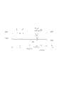
请参阅图1,本发明具有测试点的信号传输线一较佳实施例包括一对平行的信号传输线10,其包括一侵扰线11和一受扰线12,以Lm表示两信号传输线间的互感,L表示各信号传输线的感抗,Cm表示两信号传输线间的互容,C表示各信号传输线的容抗,τr表示侵扰线11中传输信号的上升沿延时,Tpd表示受扰线中串扰信号传输的时间,则远端串扰FEXT的计算如下:FEXT[%]=-Tpd/2τr×(Lm/L-Cm/C),可见侵扰线11对受扰线12在各时间点的远端串扰将随受扰线中串扰信号传输时间的增加而增大,且在各信号传输线间的各介电参数一定的条件下,所述并行信号传输线越长,Tpd越大,则其远端串扰叠加得越多。Please refer to Fig. 1, the present invention has the signal transmission line of test point one preferred embodiment to comprise a pair of parallel
图1中的侵扰线11和受扰线12的长均为h,侵扰线11包括一第一端113和一第二端115,受扰线12包括一第一端123和一第二端125,侵扰线11和受扰线12相对一一维坐标轴x平行排列,侵扰线11和受扰线12的第一端113和123与该坐标轴x的原点0对齐,则两第一端113和123的坐标均为0,两第二端115和215的坐标均为h,取两个大于零的正数a和b,使a+b=h/2;在侵扰线11的坐标为a处接入一第一测试点M1,在受扰线12的坐标为h/2-b出接入一第二测试点M2,因此第一测试点M1和第二测试点M2坐标不同,第一测试点M1在侵扰线11上的位置不同于第二测试点M2在受扰线12上的位置;在本实施例中,第一测试点M1和第二测试点M2为同样的测试点,由于测试点M1和M2的延时性,当信号传输到侵扰线11或受扰线12上的测试点M1或M2时,其会产生一段延时Td,所以信号在侵扰线11和受扰线12上传输时所受的延时相等,从而保证了信号的同步性,在一般情况下,延时Td小于或等于侵扰线11中传输信号的上升沿延时τr。The lengths of the
下面来分析上述侵扰线11和受扰线12是如何降低串扰的。Next, we will analyze how the above-mentioned
请参阅图1和图2,信号开始在高速信号传输线10上同步传输,侵扰线11上传输的信号Q1在第一端113开始传输,并同时开始在受扰线12的第一端123上产生一第一远端串扰FEXT1,第一远端串扰FEXT1与信号Q1一起向前传输,且第一远端串扰FEXT1在信号Q1的影响下随着传输距离的增加而逐渐变大,当信号Q1和第一远端串扰FEXT1传输到坐标a处时,信号Q1受到此处第一测试点M1的延时而停留在此处,第一远端串扰FEXT1继续向前传输,此时第一远端串扰FEXT1和信号Q1不再同步,第一远端串扰FEXT1不再受信号Q1的影响而保持不变。Please refer to FIG. 1 and FIG. 2, the signal starts to be transmitted synchronously on the high-speed
请参阅图3,信号Q1被第一测试点M1延时Td后继续向前传输,从而在受扰线12的坐标a出产生一第二远端串扰FEXT2,第二远端串扰FEXT2与信号Q1一起向前传输,且第二远端串扰FEXT2在信号Q1的影响下随着传输距离的增加而逐渐变大。Please refer to FIG. 3 , the signal Q1 is delayed by Td at the first test point M1 and continues to transmit forward, thereby generating a second far-end crosstalk FEXT2 at the coordinate a of the
请参阅图4,当第一远端串扰FEXT1传输到坐标h/2-b处时,第一远端串扰FEXT1受到此处第二测试点M2的延时而停留在此处,信号Q1和第二远端串扰FEXT2继续向前传输,且第二远端串扰FEXT2在信号Q1的影响下随着传输距离的增加而逐渐变大。Please refer to Figure 4, when the first far-end crosstalk FEXT1 is transmitted to the coordinate h/2-b, the first far-end crosstalk FEXT1 is delayed by the second test point M2 here and stays here, the signal Q1 and the first The second far-end crosstalk FEXT2 continues to transmit forward, and the second far-end crosstalk FEXT2 gradually becomes larger as the transmission distance increases under the influence of the signal Q1.
请参阅图5和图6,当第一远端串扰FEXT1被第二测试点M2延时Td后,信号Q1和第二远端串扰FEXT2传输到坐标h/2-b处,第二远端串扰FEXT2受到此处第二测试点M2的延时而停留在此处,信号Q1和第一远端串扰FEXT1继续向前传输,第一远端串扰FEXT1再次在信号Q1的影响下随着传输距离的增加而逐渐变大,第二远端串扰FEXT2不再受信号Q1的影响而保持不变,信号Q1和第一远端串扰FEXT1继续向前传输直至分别同时传到侵扰线11和受扰线12的第二端115和125而从信号传输线10上输出,第二远端串扰FEXT2被第二测试点M2延时Td后也向前传输到受扰线12的第二端125而输出。Please refer to Fig. 5 and Fig. 6, when the first far-end crosstalk FEXT1 is delayed by Td by the second test point M2, the signal Q1 and the second far-end crosstalk FEXT2 are transmitted to the coordinate h/2-b, and the second far-end crosstalk The crosstalk FEXT2 stays here due to the delay of the second test point M2 here, the signal Q1 and the first far-end crosstalk FEXT1 continue to transmit forward, and the first far-end crosstalk FEXT1 is again affected by the signal Q1 with the transmission distance The second far-end crosstalk FEXT2 is no longer affected by the signal Q1 and remains unchanged, and the signal Q1 and the first far-end crosstalk FEXT1 continue to transmit until they reach the
在上述的信号传输线10中,第一远端串扰FEXT1受信号Q1影响的距离为a+b=h/2,第二远端串扰FEXT2受信号Q1影响的也为h/2,则第一远端串扰FEXT1和第二远端串扰FEXT2均被减小到原来远端串扰的一半,且第一第一远端串扰FEXT1和第二远端串扰FEXT2在受扰线12上传输时并不同步,从而避免了第一远端串扰FEXT1和第二远端串扰FEXT2的完全叠加,从而使信号传输线10的串扰保持在一个较低的强度,改善了信号传输线10上信号的传输品质。In the above-mentioned
在上述实施例中,为了布线的方便可将正数a和b分别取为h/4,当然也可将正数a和b取为其它的值,只要满足a+b=h/2即可。In the above embodiment, for the convenience of wiring, the positive numbers a and b can be taken as h/4 respectively, of course, the positive numbers a and b can also be taken as other values, as long as a+b=h/2 is satisfied .
Claims (6)
Translated fromChinesePriority Applications (3)
| Application Number | Priority Date | Filing Date | Title |
|---|---|---|---|
| CN201110429414.2ACN103179776B (en) | 2011-12-20 | 2011-12-20 | Signal transmission line with test point |
| TW100148528ATWI447406B (en) | 2011-12-20 | 2011-12-26 | Signal lines with testing point |
| US13/711,415US9046550B2 (en) | 2011-12-20 | 2012-12-11 | Signal transmission lines with test pad |
Applications Claiming Priority (1)
| Application Number | Priority Date | Filing Date | Title |
|---|---|---|---|
| CN201110429414.2ACN103179776B (en) | 2011-12-20 | 2011-12-20 | Signal transmission line with test point |
Publications (2)
| Publication Number | Publication Date |
|---|---|
| CN103179776Atrue CN103179776A (en) | 2013-06-26 |
| CN103179776B CN103179776B (en) | 2016-04-06 |
Family
ID=48609503
Family Applications (1)
| Application Number | Title | Priority Date | Filing Date |
|---|---|---|---|
| CN201110429414.2AExpired - Fee RelatedCN103179776B (en) | 2011-12-20 | 2011-12-20 | Signal transmission line with test point |
Country Status (3)
| Country | Link |
|---|---|
| US (1) | US9046550B2 (en) |
| CN (1) | CN103179776B (en) |
| TW (1) | TWI447406B (en) |
Cited By (1)
| Publication number | Priority date | Publication date | Assignee | Title |
|---|---|---|---|---|
| CN110554247A (en)* | 2019-08-28 | 2019-12-10 | 广州广电计量检测股份有限公司 | crosstalk simulation modeling method and simulation model of non-parallel cable |
Citations (6)
| Publication number | Priority date | Publication date | Assignee | Title |
|---|---|---|---|---|
| US5961355A (en)* | 1997-12-17 | 1999-10-05 | Berg Technology, Inc. | High density interstitial connector system |
| TW521148B (en)* | 2001-09-06 | 2003-02-21 | Mitac Int Corp | Testing point setup method of high-frequency differential signal |
| US20060284697A1 (en)* | 2005-06-17 | 2006-12-21 | Hon Hai Precision Industry Co., Ltd. | Layout configuration of differential signal transmission lines for printed circuit board |
| CN1953639A (en)* | 2005-10-17 | 2007-04-25 | 鸿富锦精密工业(深圳)有限公司 | A wiring structure and method to reduce the far-end cross talk between parallel signal circuits |
| CN101621047A (en)* | 2008-07-04 | 2010-01-06 | 鸿富锦精密工业(深圳)有限公司 | Framework for reducing far end crosstalk between signal circuits |
| CN102196662A (en)* | 2010-02-23 | 2011-09-21 | 弗莱克斯电子有限责任公司 | Test point design for a high speed bus |
Family Cites Families (3)
| Publication number | Priority date | Publication date | Assignee | Title |
|---|---|---|---|---|
| US3714572A (en)* | 1970-08-21 | 1973-01-30 | Rca Corp | Alignment and test fixture apparatus |
| CN101082638B (en)* | 2006-06-01 | 2010-05-12 | 英业达股份有限公司 | Transmission line for internal circuit test point |
| TWI396028B (en)* | 2009-11-25 | 2013-05-11 | Au Optronics Corp | An array, probe for testing the array and liquid crystal display panel |
- 2011
- 2011-12-20CNCN201110429414.2Apatent/CN103179776B/ennot_activeExpired - Fee Related
- 2011-12-26TWTW100148528Apatent/TWI447406B/ennot_activeIP Right Cessation
- 2012
- 2012-12-11USUS13/711,415patent/US9046550B2/ennot_activeExpired - Fee Related
Patent Citations (6)
| Publication number | Priority date | Publication date | Assignee | Title |
|---|---|---|---|---|
| US5961355A (en)* | 1997-12-17 | 1999-10-05 | Berg Technology, Inc. | High density interstitial connector system |
| TW521148B (en)* | 2001-09-06 | 2003-02-21 | Mitac Int Corp | Testing point setup method of high-frequency differential signal |
| US20060284697A1 (en)* | 2005-06-17 | 2006-12-21 | Hon Hai Precision Industry Co., Ltd. | Layout configuration of differential signal transmission lines for printed circuit board |
| CN1953639A (en)* | 2005-10-17 | 2007-04-25 | 鸿富锦精密工业(深圳)有限公司 | A wiring structure and method to reduce the far-end cross talk between parallel signal circuits |
| CN101621047A (en)* | 2008-07-04 | 2010-01-06 | 鸿富锦精密工业(深圳)有限公司 | Framework for reducing far end crosstalk between signal circuits |
| CN102196662A (en)* | 2010-02-23 | 2011-09-21 | 弗莱克斯电子有限责任公司 | Test point design for a high speed bus |
Cited By (1)
| Publication number | Priority date | Publication date | Assignee | Title |
|---|---|---|---|---|
| CN110554247A (en)* | 2019-08-28 | 2019-12-10 | 广州广电计量检测股份有限公司 | crosstalk simulation modeling method and simulation model of non-parallel cable |
Also Published As
| Publication number | Publication date |
|---|---|
| US9046550B2 (en) | 2015-06-02 |
| US20130154680A1 (en) | 2013-06-20 |
| CN103179776B (en) | 2016-04-06 |
| TW201326841A (en) | 2013-07-01 |
| TWI447406B (en) | 2014-08-01 |
Similar Documents
| Publication | Publication Date | Title |
|---|---|---|
| US8159310B2 (en) | Mictostrip transmission line structure with vertical stubs for reducing far-end crosstalk | |
| CN104182576B (en) | Design method for reducing crosstalk influence between high-speed differential pairs | |
| CN103188861B (en) | Lay the printed circuit board (PCB) of differential pair | |
| US9722643B2 (en) | Enhanced echo cancellation in full-duplex communication | |
| CN104582290A (en) | Method for realizing high-speed line impedance continuity | |
| CN104102797A (en) | PCB (printed circuit board) layout design method reducing differential crosstalk | |
| CN102083277A (en) | Printed circuit board and wiring method thereof | |
| TWI528742B (en) | Emi suppression device and method for network transmission | |
| CN103179776B (en) | Signal transmission line with test point | |
| CN102056404B (en) | Method for neutralizing capacitance of through hole | |
| CN104244598A (en) | Method and device for controlling impedance continuity of transmission line on PCB (printed circuit board) | |
| CN104239632B (en) | A kind of method of reduction VGA cabling cross talk effects signals | |
| CN110162819A (en) | A kind of EMC analysis method based on improved system method | |
| CN105335587A (en) | Chip Pinout design method for inhibiting signal crosstalk noise | |
| Wu et al. | High speed muti-board signal integrity simulation and implementation | |
| Wang et al. | Crosstalk analysis in signal integrity | |
| CN104244610A (en) | A design method to reduce the impact of CONNECTOR vias | |
| US7961062B2 (en) | Aggressor/victim transmission line pair having spaced time delay modules for providing cross-talk reduction | |
| TW201311076A (en) | Topology structure of multiple loads | |
| US9160048B2 (en) | Electronic device with terminal circuits | |
| Huang et al. | Signal integrity improvements of bended coupled lines by using miniaturized capacitance and inductance compensation structures | |
| US9236645B2 (en) | Serpentine delay line structure | |
| CN210137305U (en) | Improved VGA topology design system | |
| CN107506554B (en) | A printed circuit board applied to a storage system and its wiring method and device | |
| Nieh et al. | Far-end crosstalk cancellation using via stub for DDR4 memory channel |
Legal Events
| Date | Code | Title | Description |
|---|---|---|---|
| C06 | Publication | ||
| PB01 | Publication | ||
| C10 | Entry into substantive examination | ||
| SE01 | Entry into force of request for substantive examination | ||
| C14 | Grant of patent or utility model | ||
| GR01 | Patent grant | ||
| TR01 | Transfer of patent right | Effective date of registration:20170614 Address after:Floor 3, building 3, Jin Ye street, Pingnan industrial area, three Town, Zhongshan, Guangdong Patentee after:Kai Xiang Electronics Co., Ltd. of Zhongshan city Address before:430205 Hubei city of Wuhan province Optics Valley East Lake New Technology Development Zone Road No. two Foxconn Technology Park Co-patentee before:Hon Hai Precision Industry Co., Ltd. Patentee before:Hongfujin Precision Industry (Wuhan) Co., Ltd. | |
| TR01 | Transfer of patent right | ||
| CF01 | Termination of patent right due to non-payment of annual fee | Granted publication date:20160406 Termination date:20181220 | |
| CF01 | Termination of patent right due to non-payment of annual fee |