CN103178204A - Solid-liquid diffusion bonding structure of thermoelectric module and method for manufacturing same - Google Patents
Solid-liquid diffusion bonding structure of thermoelectric module and method for manufacturing sameDownload PDFInfo
- Publication number
- CN103178204A CN103178204ACN2011104470801ACN201110447080ACN103178204ACN 103178204 ACN103178204 ACN 103178204ACN 2011104470801 ACN2011104470801 ACN 2011104470801ACN 201110447080 ACN201110447080 ACN 201110447080ACN 103178204 ACN103178204 ACN 103178204A
- Authority
- CN
- China
- Prior art keywords
- silver
- nickel
- metal film
- tin
- solid
- Prior art date
- Legal status (The legal status is an assumption and is not a legal conclusion. Google has not performed a legal analysis and makes no representation as to the accuracy of the status listed.)
- Granted
Links
Images


Classifications
- B—PERFORMING OPERATIONS; TRANSPORTING
- B23—MACHINE TOOLS; METAL-WORKING NOT OTHERWISE PROVIDED FOR
- B23K—SOLDERING OR UNSOLDERING; WELDING; CLADDING OR PLATING BY SOLDERING OR WELDING; CUTTING BY APPLYING HEAT LOCALLY, e.g. FLAME CUTTING; WORKING BY LASER BEAM
- B23K20/00—Non-electric welding by applying impact or other pressure, with or without the application of heat, e.g. cladding or plating
- B23K20/02—Non-electric welding by applying impact or other pressure, with or without the application of heat, e.g. cladding or plating by means of a press ; Diffusion bonding
- B23K20/023—Thermo-compression bonding
- B23K20/026—Thermo-compression bonding with diffusion of soldering material
- B—PERFORMING OPERATIONS; TRANSPORTING
- B23—MACHINE TOOLS; METAL-WORKING NOT OTHERWISE PROVIDED FOR
- B23K—SOLDERING OR UNSOLDERING; WELDING; CLADDING OR PLATING BY SOLDERING OR WELDING; CUTTING BY APPLYING HEAT LOCALLY, e.g. FLAME CUTTING; WORKING BY LASER BEAM
- B23K20/00—Non-electric welding by applying impact or other pressure, with or without the application of heat, e.g. cladding or plating
- B23K20/16—Non-electric welding by applying impact or other pressure, with or without the application of heat, e.g. cladding or plating with interposition of special material to facilitate connection of the parts, e.g. material for absorbing or producing gas
- B—PERFORMING OPERATIONS; TRANSPORTING
- B23—MACHINE TOOLS; METAL-WORKING NOT OTHERWISE PROVIDED FOR
- B23K—SOLDERING OR UNSOLDERING; WELDING; CLADDING OR PLATING BY SOLDERING OR WELDING; CUTTING BY APPLYING HEAT LOCALLY, e.g. FLAME CUTTING; WORKING BY LASER BEAM
- B23K20/00—Non-electric welding by applying impact or other pressure, with or without the application of heat, e.g. cladding or plating
- B23K20/22—Non-electric welding by applying impact or other pressure, with or without the application of heat, e.g. cladding or plating taking account of the properties of the materials to be welded
- B23K20/233—Non-electric welding by applying impact or other pressure, with or without the application of heat, e.g. cladding or plating taking account of the properties of the materials to be welded without ferrous layer
- B—PERFORMING OPERATIONS; TRANSPORTING
- B23—MACHINE TOOLS; METAL-WORKING NOT OTHERWISE PROVIDED FOR
- B23K—SOLDERING OR UNSOLDERING; WELDING; CLADDING OR PLATING BY SOLDERING OR WELDING; CUTTING BY APPLYING HEAT LOCALLY, e.g. FLAME CUTTING; WORKING BY LASER BEAM
- B23K20/00—Non-electric welding by applying impact or other pressure, with or without the application of heat, e.g. cladding or plating
- B23K20/24—Preliminary treatment
- B—PERFORMING OPERATIONS; TRANSPORTING
- B23—MACHINE TOOLS; METAL-WORKING NOT OTHERWISE PROVIDED FOR
- B23K—SOLDERING OR UNSOLDERING; WELDING; CLADDING OR PLATING BY SOLDERING OR WELDING; CUTTING BY APPLYING HEAT LOCALLY, e.g. FLAME CUTTING; WORKING BY LASER BEAM
- B23K35/00—Rods, electrodes, materials, or media, for use in soldering, welding, or cutting
- B23K35/001—Interlayers, transition pieces for metallurgical bonding of workpieces
- B23K35/004—Interlayers, transition pieces for metallurgical bonding of workpieces at least one of the workpieces being of a metal of the iron group
- B—PERFORMING OPERATIONS; TRANSPORTING
- B23—MACHINE TOOLS; METAL-WORKING NOT OTHERWISE PROVIDED FOR
- B23K—SOLDERING OR UNSOLDERING; WELDING; CLADDING OR PLATING BY SOLDERING OR WELDING; CUTTING BY APPLYING HEAT LOCALLY, e.g. FLAME CUTTING; WORKING BY LASER BEAM
- B23K35/00—Rods, electrodes, materials, or media, for use in soldering, welding, or cutting
- B23K35/001—Interlayers, transition pieces for metallurgical bonding of workpieces
- B23K35/007—Interlayers, transition pieces for metallurgical bonding of workpieces at least one of the workpieces being of copper or another noble metal
- B—PERFORMING OPERATIONS; TRANSPORTING
- B23—MACHINE TOOLS; METAL-WORKING NOT OTHERWISE PROVIDED FOR
- B23K—SOLDERING OR UNSOLDERING; WELDING; CLADDING OR PLATING BY SOLDERING OR WELDING; CUTTING BY APPLYING HEAT LOCALLY, e.g. FLAME CUTTING; WORKING BY LASER BEAM
- B23K35/00—Rods, electrodes, materials, or media, for use in soldering, welding, or cutting
- B23K35/22—Rods, electrodes, materials, or media, for use in soldering, welding, or cutting characterised by the composition or nature of the material
- B23K35/24—Selection of soldering or welding materials proper
- B23K35/26—Selection of soldering or welding materials proper with the principal constituent melting at less than 400 degrees C
- B23K35/262—Sn as the principal constituent
- B—PERFORMING OPERATIONS; TRANSPORTING
- B23—MACHINE TOOLS; METAL-WORKING NOT OTHERWISE PROVIDED FOR
- B23K—SOLDERING OR UNSOLDERING; WELDING; CLADDING OR PLATING BY SOLDERING OR WELDING; CUTTING BY APPLYING HEAT LOCALLY, e.g. FLAME CUTTING; WORKING BY LASER BEAM
- B23K35/00—Rods, electrodes, materials, or media, for use in soldering, welding, or cutting
- B23K35/22—Rods, electrodes, materials, or media, for use in soldering, welding, or cutting characterised by the composition or nature of the material
- B23K35/24—Selection of soldering or welding materials proper
- B23K35/30—Selection of soldering or welding materials proper with the principal constituent melting at less than 1550 degrees C
- B23K35/3006—Ag as the principal constituent
- B—PERFORMING OPERATIONS; TRANSPORTING
- B23—MACHINE TOOLS; METAL-WORKING NOT OTHERWISE PROVIDED FOR
- B23K—SOLDERING OR UNSOLDERING; WELDING; CLADDING OR PLATING BY SOLDERING OR WELDING; CUTTING BY APPLYING HEAT LOCALLY, e.g. FLAME CUTTING; WORKING BY LASER BEAM
- B23K35/00—Rods, electrodes, materials, or media, for use in soldering, welding, or cutting
- B23K35/22—Rods, electrodes, materials, or media, for use in soldering, welding, or cutting characterised by the composition or nature of the material
- B23K35/24—Selection of soldering or welding materials proper
- B23K35/30—Selection of soldering or welding materials proper with the principal constituent melting at less than 1550 degrees C
- B23K35/302—Cu as the principal constituent
- B—PERFORMING OPERATIONS; TRANSPORTING
- B23—MACHINE TOOLS; METAL-WORKING NOT OTHERWISE PROVIDED FOR
- B23K—SOLDERING OR UNSOLDERING; WELDING; CLADDING OR PLATING BY SOLDERING OR WELDING; CUTTING BY APPLYING HEAT LOCALLY, e.g. FLAME CUTTING; WORKING BY LASER BEAM
- B23K35/00—Rods, electrodes, materials, or media, for use in soldering, welding, or cutting
- B23K35/22—Rods, electrodes, materials, or media, for use in soldering, welding, or cutting characterised by the composition or nature of the material
- B23K35/24—Selection of soldering or welding materials proper
- B23K35/30—Selection of soldering or welding materials proper with the principal constituent melting at less than 1550 degrees C
- B23K35/3033—Ni as the principal constituent
- B—PERFORMING OPERATIONS; TRANSPORTING
- B32—LAYERED PRODUCTS
- B32B—LAYERED PRODUCTS, i.e. PRODUCTS BUILT-UP OF STRATA OF FLAT OR NON-FLAT, e.g. CELLULAR OR HONEYCOMB, FORM
- B32B15/00—Layered products comprising a layer of metal
- B32B15/01—Layered products comprising a layer of metal all layers being exclusively metallic
- H—ELECTRICITY
- H10—SEMICONDUCTOR DEVICES; ELECTRIC SOLID-STATE DEVICES NOT OTHERWISE PROVIDED FOR
- H10N—ELECTRIC SOLID-STATE DEVICES NOT OTHERWISE PROVIDED FOR
- H10N10/00—Thermoelectric devices comprising a junction of dissimilar materials, i.e. devices exhibiting Seebeck or Peltier effects
- H10N10/01—Manufacture or treatment
- H—ELECTRICITY
- H10—SEMICONDUCTOR DEVICES; ELECTRIC SOLID-STATE DEVICES NOT OTHERWISE PROVIDED FOR
- H10N—ELECTRIC SOLID-STATE DEVICES NOT OTHERWISE PROVIDED FOR
- H10N10/00—Thermoelectric devices comprising a junction of dissimilar materials, i.e. devices exhibiting Seebeck or Peltier effects
- H10N10/80—Constructional details
- H10N10/81—Structural details of the junction
- H10N10/817—Structural details of the junction the junction being non-separable, e.g. being cemented, sintered or soldered
- H—ELECTRICITY
- H10—SEMICONDUCTOR DEVICES; ELECTRIC SOLID-STATE DEVICES NOT OTHERWISE PROVIDED FOR
- H10N—ELECTRIC SOLID-STATE DEVICES NOT OTHERWISE PROVIDED FOR
- H10N10/00—Thermoelectric devices comprising a junction of dissimilar materials, i.e. devices exhibiting Seebeck or Peltier effects
- H10N10/80—Constructional details
- H10N10/85—Thermoelectric active materials
- H10N10/851—Thermoelectric active materials comprising inorganic compositions
- H10N10/852—Thermoelectric active materials comprising inorganic compositions comprising tellurium, selenium or sulfur
- B—PERFORMING OPERATIONS; TRANSPORTING
- B23—MACHINE TOOLS; METAL-WORKING NOT OTHERWISE PROVIDED FOR
- B23K—SOLDERING OR UNSOLDERING; WELDING; CLADDING OR PLATING BY SOLDERING OR WELDING; CUTTING BY APPLYING HEAT LOCALLY, e.g. FLAME CUTTING; WORKING BY LASER BEAM
- B23K2101/00—Articles made by soldering, welding or cutting
- B23K2101/36—Electric or electronic devices
- B—PERFORMING OPERATIONS; TRANSPORTING
- B23—MACHINE TOOLS; METAL-WORKING NOT OTHERWISE PROVIDED FOR
- B23K—SOLDERING OR UNSOLDERING; WELDING; CLADDING OR PLATING BY SOLDERING OR WELDING; CUTTING BY APPLYING HEAT LOCALLY, e.g. FLAME CUTTING; WORKING BY LASER BEAM
- B23K2103/00—Materials to be soldered, welded or cut
- B23K2103/08—Non-ferrous metals or alloys
- B23K2103/12—Copper or alloys thereof
- B—PERFORMING OPERATIONS; TRANSPORTING
- B23—MACHINE TOOLS; METAL-WORKING NOT OTHERWISE PROVIDED FOR
- B23K—SOLDERING OR UNSOLDERING; WELDING; CLADDING OR PLATING BY SOLDERING OR WELDING; CUTTING BY APPLYING HEAT LOCALLY, e.g. FLAME CUTTING; WORKING BY LASER BEAM
- B23K2103/00—Materials to be soldered, welded or cut
- B23K2103/18—Dissimilar materials
Landscapes
- Engineering & Computer Science (AREA)
- Mechanical Engineering (AREA)
- Chemical & Material Sciences (AREA)
- Inorganic Chemistry (AREA)
- Manufacturing & Machinery (AREA)
- Pressure Welding/Diffusion-Bonding (AREA)
- Connection Of Batteries Or Terminals (AREA)
- Measuring Temperature Or Quantity Of Heat (AREA)
Abstract
Translated fromChinese
Description
Translated fromChinese技术领域technical field
本发明涉及一种热电模块的固液扩散接合结构及其制造方法。The invention relates to a solid-liquid diffusion bonding structure of a thermoelectric module and a manufacturing method thereof.
背景技术Background technique
单一热电元件能够传输或转换的热电非常有限,因此一般会利用金属电极将多组热电元件连结以形成热电模块,如此才能够提供足够的热电传输功率。The thermoelectricity that can be transmitted or converted by a single thermoelectric element is very limited. Therefore, metal electrodes are generally used to connect multiple sets of thermoelectric elements to form a thermoelectric module, so as to provide sufficient thermoelectric transmission power.
传统针对热电元件与电极的接合是采用软焊(soldering)接合方法。例如在US5,429,680、US5,441,576、US5,817,188、US6,103,967以及US3,079,455。上述现有技术都是使用低熔点且厚度高达数厘米以上的锡或是焊锡合金在摄氏300度左右的条件下进行接合,在接合之后,低熔点的锡或是焊锡合金仍会部分残留。此种采用焊锡接合的方式所产生的热应力小,但缺点是热电模块的运作温度将受限于焊锡合金的熔点。换言之,采用传统焊锡方式的热电元件必需于低于焊锡合金的熔点条件下运作。Traditionally, soldering is used for joining thermoelectric elements and electrodes. For example in US5,429,680, US5,441,576, US5,817,188, US6,103,967 and US3,079,455. The above-mentioned prior art uses tin or solder alloy with a low melting point and a thickness of several centimeters or more for bonding at about 300 degrees Celsius. After bonding, the tin or solder alloy with a low melting point still partially remains. The thermal stress generated by this method of solder joint is small, but the disadvantage is that the operating temperature of the thermoelectric module is limited by the melting point of the solder alloy. In other words, the thermoelectric element adopting the traditional solder method must operate under the condition lower than the melting point of the solder alloy.
为了提高热电元件的使用温度,现有技术,例如US6,492,585,是采用硬焊(brazing)接合方法,亦即使用较高熔点的填充金属,以提高接合点所能承受的温度。但是此种方法的接合程序的温度必需高达摄氏450度以上。当接合程序完成并冷却到室温时,热电材料与金属电极之间的热膨胀系数差异将会产生相当大的热应力,进而造成接合界面的损坏。In order to increase the operating temperature of thermoelectric elements, the prior art, such as US6,492,585, adopts a brazing joining method, that is, using a filler metal with a higher melting point to increase the temperature that the joint can withstand. However, the temperature of the bonding procedure of this method must be as high as 450 degrees Celsius or more. When the bonding procedure is completed and cooled to room temperature, the difference in thermal expansion coefficient between the thermoelectric material and the metal electrode will generate considerable thermal stress, which in turn will cause damage to the bonding interface.
针对固液扩散接合(solid liquid inter-diffusion,SLID)技术,最早在1966年由L.Bernston等学者发表在期刊以将SLID技术应用于集成电路中。此外,US6,234,378采用Au-In合金系统应用于激光回转仪,以接合石英、陶瓷与金属材料零组件,以解决热膨胀系数不同的问题并且提升元件在高温的操作性能。再者,US2003/0160021则是将SLID技术应用于微机电(MEMS)元件,其先在芯片与接合物上镀上Cr,再镀上Au或In,最后形成Au-In合金,以达到高接合强度与高温应用。For solid liquid inter-diffusion (SLID) technology, it was first published in journals by scholars such as L. Bernston in 1966 to apply SLID technology to integrated circuits. In addition, US6,234,378 uses an Au-In alloy system to apply to a laser gyroscope to join quartz, ceramic and metal components to solve the problem of different thermal expansion coefficients and improve the operating performance of components at high temperatures. Furthermore, US2003/0160021 applies SLID technology to micro-electromechanical (MEMS) components, which first plate Cr on the chip and the bond, then plate Au or In, and finally form an Au-In alloy to achieve high bonding strength and high temperature applications.
发明内容Contents of the invention
本发明的目的在于提供一种热电模块的固液扩散接合结构及其制造方法,其可以在低温条件下进行接合并且所形成的热电模块可以在高温条件下使用。The object of the present invention is to provide a thermoelectric module solid-liquid diffusion bonding structure and its manufacturing method, which can be bonded under low temperature conditions and the formed thermoelectric module can be used under high temperature conditions.
为达上述目的,本发明提出一种热电模块的固液扩散接合结构的制造方法,此方法包括于热电元件以及电极板两者至少其中之一先形成银、镍或是铜金属薄膜,再形成锡金属薄膜。将热电元件与电极板堆叠在一起并且进行压合以及加热处理程序,以使得锡金属薄膜与银、镍或是铜金属薄膜反应形成银锡、镍锡或铜锡合金的金属间化合物。进行冷却步骤,以使热电元件以及电极板接合在一起。在此,低熔点锡金属薄膜完全反应而形成较高熔点金属间化合物,且银、镍或是铜金属薄膜仍有部分残留。In order to achieve the above purpose, the present invention proposes a method for manufacturing a solid-liquid diffusion bonding structure of a thermoelectric module. This method includes forming a silver, nickel or copper metal film on at least one of the thermoelectric element and the electrode plate, and then forming tin metal film. The thermoelectric element and the electrode plate are stacked together and subjected to pressing and heat treatment procedures, so that the tin metal film reacts with the silver, nickel or copper metal film to form an intermetallic compound of silver tin, nickel tin or copper tin alloy. A cooling step is performed to bond the thermoelectric elements and electrode plates together. Here, the low-melting-point tin metal film reacts completely to form a higher-melting-point intermetallic compound, and the silver, nickel or copper metal film still partially remains.
本发明提出一种热电模块的固液扩散接合结构,此结构包括至少一热电元件以及至少一电极板。所述热电元件与所述电极板之间具有接合层以使两者接合在一起,其中所述接合层包括银锡金属间化合物、镍锡金属间化合物或是铜锡金属间化合物。The invention provides a solid-liquid diffusion bonding structure of a thermoelectric module, which includes at least one thermoelectric element and at least one electrode plate. A bonding layer is provided between the thermoelectric element and the electrode plate to bond them together, wherein the bonding layer includes silver-tin intermetallic compound, nickel-tin intermetallic compound or copper-tin intermetallic compound.
基于上述,本发明的热电模块的固液扩散接合结构及其制造方法可以在低温条件下使低熔点的锡融化而与银、镍或是铜反应以形成具有高熔点的银锡金属间化合物、镍锡金属间化合物或是铜锡金属间化合物的接合层。因此本发明可以在低温条件下进行接合并且所形成的热电模块可以在高温条件下使用。Based on the above, the solid-liquid diffusion bonding structure of the thermoelectric module of the present invention and its manufacturing method can melt tin with a low melting point under low temperature conditions to react with silver, nickel or copper to form silver-tin intermetallic compounds with a high melting point, Bonding layer of nickel-tin intermetallic or copper-tin intermetallic. Therefore, the present invention can be bonded under low temperature conditions and the formed thermoelectric module can be used under high temperature conditions.
为让本发明的上述特征和优点能更明显易懂,下文特举实施例,并配合所附附图作详细说明如下。In order to make the above-mentioned features and advantages of the present invention more comprehensible, the following specific embodiments are described in detail together with the accompanying drawings.
附图说明Description of drawings
图1至图4是根据本发明一实施例的热电模块的固液扩散接合结构的制造流程示意图。1 to 4 are schematic diagrams of the manufacturing process of the solid-liquid diffusion bonding structure of the thermoelectric module according to an embodiment of the present invention.
主要元件符号说明Description of main component symbols
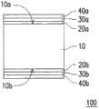
10:热电元件10: thermoelectric element
10a:第一表面10a: first surface
10b:第二表面10b: Second surface
20a,20b:阻障层20a, 20b: barrier layer
30a,30b:银、镍或是铜金属薄膜30a, 30b: silver, nickel or copper metal film
40a,40b:锡金属薄膜40a, 40b: tin metal film
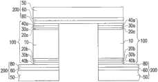
100:堆叠结构100: stacked structure
50:电极板50: electrode plate
60:银、镍或是铜金属薄膜60: silver, nickel or copper metal film
80:锡金属薄膜80: tin metal film
200:堆叠结构200: stacked structure
90a,90b:接合层90a, 90b: bonding layer
具体实施方式Detailed ways
图1至图4是根据本发明一实施例的热电模块的固液扩散接合结构的制造流程示意图。请参照图1,本实施例的热电模块的固液扩散接合结构的制造方法包括提供至少一热电元件10。根据本实施例,所述热电元件10包括可将热转换为电的材料,其可为P型热电材料或是N型热电材料,举例来说,热电元件10包括Bi2Te3、GeTe、PbTe、CoSb3或Zn4Sb3系列合金材料,但本发明不限于此。1 to 4 are schematic diagrams of the manufacturing process of the solid-liquid diffusion bonding structure of the thermoelectric module according to an embodiment of the present invention. Referring to FIG. 1 , the manufacturing method of the solid-liquid diffusion bonding structure of the thermoelectric module of the present embodiment includes providing at least one
承上所述,热电元件10包括第一表面10a以及第二表面10b。接着,于热电元件10的第一表面10a上形成银、镍或是铜金属薄膜30a以及锡金属薄膜40a,较佳的是在热电元件10的第一表面10a上还进一步包括形成有阻障层20a。在本实施例中,银、镍或是铜金属薄膜30a的厚度为2~10微米,且锡金属薄膜40a的厚度为1~10微米。另外,阻障层20a的材质包括镍或是其他合适的可阻障金属元素扩散的金属材料,且厚度例如是1~5微米。As mentioned above, the
在本实施例中,除了在热电元件10的第一表面10a上形成银、镍或是铜金属薄膜30a以及锡金属薄膜40a之外,还在热电元件10的第二表面10b上形成银、镍或是铜金属薄膜30b以及锡金属薄膜40b,较佳的是在热电元件10的第二表面10b上还进一步包括阻障层20b。银、镍或是铜金属薄膜30b的厚度为2~10微米,且锡金属薄膜40b的厚度为1~10微米。另外,阻障层20b包括镍或是其他合适的可阻障金属元素扩散的金属材料,且厚度例如是1~5微米。于热电元件10的第一表面10a上形成银、镍或是铜金属薄膜30a以及锡金属薄膜40a以及热电元件10的第二表面10b上形成银、镍或是铜金属薄膜30b以及锡金属薄膜40b的方法包括电镀程序、无电镀程序、溅镀用或化学气相沉积程序。In this embodiment, in addition to forming silver, nickel or
上述于热电元件10的第一表面10a形成阻障层20a、银、镍或是铜金属薄膜30a以及锡金属薄膜40a,并且于第二表面10b形成阻障层20b、银、镍或是铜金属薄膜30b以及锡金属薄膜40b之后即构成堆叠结构100。The
另外,请参照图2,提供至少一电极板50,所述电极板50例如是铜电极板或是其他金属材料电极板。接着于电极板50的表面上形成银、镍或是铜金属薄膜60以及锡金属薄膜80。银、镍或是铜金属薄膜60的厚度为2~10微米,且锡金属薄膜80的厚度为1~10微米。上述于电极板50上形成银、镍或是铜金属薄膜60以及锡金属薄膜80之后即构成堆叠结构200。于电极板50的表面形成银、镍或是铜金属薄膜60以及锡金属薄膜80的方法包括电镀程序、无电镀程序、溅镀用或化学气相沉积程序。In addition, referring to FIG. 2 , at least one
值得一提的是,在图1的实施例中,具有热电元件10的堆叠结构100中是形成有银、镍或是铜金属薄膜30a、30b以及锡金属薄膜40a,40b,且具有电极板50的堆叠结构200是形成有银、镍或是铜金属薄膜60以及锡金属薄膜80,但本发明不限于此。在另一实施例中,所述具有热电元件10的堆叠结构100可以仅包括银、镍或是铜金属薄膜30a、30b,且在具有电极板50的堆叠结构200包括银、镍或是铜金属薄膜60以及锡金属薄膜80两膜层。根据又一实施例,所述具有热电元件10的堆叠结构100包括银、镍或是铜金属薄膜30a、30b以及锡金属薄膜40a,40b,且在具有电极板50的堆叠结构200仅包括银、镍或是铜金属薄膜60。换言之,本发明可以在热电元件10以及电极板50其中之一的表面上形成锡金属薄膜或是两者的表面上形成锡金属薄膜。It is worth mentioning that, in the embodiment of FIG. 1 , the
接着,请参照图3,将热电元件10(堆叠结构100)与电极板50(堆叠结构200)堆叠在一起以使得热电元件10上的锡金属薄膜40a,40b与电极板50的锡金属薄膜80接触。Next, referring to FIG. 3 , the thermoelectric element 10 (stack structure 100 ) and the electrode plate 50 (stack structure 200 ) are stacked together so that the
在本实施例中,每一个热电元件10(堆叠结构100)的两侧各自与一个电极板50(堆叠结构200)堆叠在一起。因此当多个热电元件10(堆叠结构100)与多个电极板50(堆叠结构200)彼此堆叠在一起之后即可形成热电模块。本实施例的图示是以两个热电元件10(堆叠结构100)与三个电极板50(堆叠结构200)堆叠为例来说明,但本发明不限制热电模块中的热电元件10(堆叠结构100)与电极板50(堆叠结构200)的数目。In this embodiment, each thermoelectric element 10 (stack structure 100 ) is stacked with an electrode plate 50 (stack structure 200 ) on both sides. Therefore, a thermoelectric module can be formed when a plurality of thermoelectric elements 10 (stack structure 100 ) and a plurality of electrode plates 50 (stack structure 200 ) are stacked together. The diagram of this embodiment is illustrated by stacking two thermoelectric elements 10 (stack structure 100) and three electrode plates 50 (stack structure 200) as an example, but the present invention does not limit the thermoelectric elements 10 (stack structure 200) in the thermoelectric module 100) and the number of electrode plates 50 (stack structure 200).
接着,如图4所示,进行压合以及加热处理程序,以使得锡金属薄膜40a,40b以及锡金属薄膜80与位于其上银、镍或是铜金属薄膜30a,30b以及位于其下的银、镍或是铜金属薄膜60反应以形成银锡金属间化合物、镍锡金属间化合物或是铜锡金属间化合物。接着冷却至室温之后,即形成具有银锡金属间化合物、镍锡金属间化合物或是铜锡金属间化合物的接合层90a,90b,使得热电元件10与电路板50接合在一起。Then, as shown in Figure 4, carry out laminating and heat treatment procedure, so that
根据本实施例,上述的压合以及加热处理程序的温度为摄氏235~350度,且时间为3~60分钟。另外,上述的压合以及加热处理程序例如是在真空环境或是惰性气体环境中进行,且加热的温度为高于锡金属薄膜的熔点的温度。当于进行压合以及加热处理程序时,低熔点的锡金属薄膜会被熔融而与高熔点的银、镍或铜金属薄膜进行界面反应,且所述界面反应会将锡金属薄膜完全消耗而形成含锡金属间化合物。上述的接合程序又可称为固液扩散接合程序(liquid inter-diffusion bonding process)。According to this embodiment, the temperature of the above pressing and heating process is 235-350 degrees Celsius, and the time is 3-60 minutes. In addition, the above-mentioned pressing and heat treatment procedures are, for example, carried out in a vacuum environment or an inert gas environment, and the heating temperature is higher than the melting point of the tin metal film. When performing pressing and heat treatment procedures, the tin metal film with a low melting point will be melted and react with the silver, nickel or copper metal film with a high melting point, and the interfacial reaction will completely consume the tin metal film to form Tin-containing intermetallic compounds. The above-mentioned bonding procedure can also be called a solid-liquid diffusion bonding procedure (liquid inter-diffusion bonding process).
更详细而言,倘若银、镍或是铜金属薄膜30a,30b,60是选用银金属,那么所述银金属薄膜30a,30b,60需足以使锡金属薄膜40a,40b,80完全反应以形成金属间化合物。更详细来说,银金属薄膜30a,30b,60以及锡金属薄膜40a,40b,80之间则需考虑使Ag∶Sn的原子比为高于3∶1。如此一来,当于进行压合以及加热处理程序时,低熔点的锡金属薄膜40a,40b,80被熔融之后可与高熔点银金属薄膜30a,30b,60反应并且完全消耗掉,最后即可形成Ag3Sn金属间化合物,且银金属薄膜30a,30b,60不会完全反应而仍有部分残留。值得一提的是,倘若银、镍或是铜金属薄膜30a,30b,60是选用银金属,在经过约为摄氏235~350度的加压加热处理程序之后所形成的银锡金属间化合物(Ag3Sn)的熔点可达摄氏480度。换言之,采用此种结合结构的热电模块可以在低于摄氏480度下使用或是操作。In more detail, if the silver, nickel or
倘若银、镍或是铜金属薄膜30a,30b,60是选择镍金属,于固液扩散接合程序之后所形成的镍锡金属间化合物可为Ni3Sn4、Ni3Sn2、Ni3Sn或是其组合。在此,所述镍金属薄膜30a,30b,60需足以使锡金属薄膜40a,40b,80完全反应以形成金属间化合物。更详细来说,镍金属薄膜30a,30b,60以及锡金属薄膜40a,40b,80之间则需考虑使Ni∶Sn的原子比为高于3∶4。如此一来,当在进行压合以及加热处理程序时,低熔点的锡金属薄膜40a,40b,80被熔融之后可与高熔点镍金属薄膜30a,30b,60反应并且完全消耗掉,最后即可形成镍锡金属间化合物(Ni3Sn4、Ni3Sn2、Ni3Sn或是其组合),且镍金属薄膜30a,30b,60不会完全反应而仍有部分残留。值得一提的是,若银、镍或是铜金属薄膜30a,30b,60是选择镍金属,于经过约为摄氏235~350度的加压加热处理程序之后所形成的镍锡金属间化合物(Ni3Sn4)的熔点可达摄氏796度,镍锡金属间化合物(Ni3Sn2)的熔点可达摄氏1267度,且镍锡金属间化合物(Ni3Sn)的熔点可达摄氏1169度。换言之,采用此种结合结构的热电模块可以在低于摄氏796度下使用或是操作。If the silver, nickel or
倘若银、镍或是铜金属薄膜30a,30b,60是选择铜金属,在固液扩散接合程序之后所形成的铜锡金属间化合物可为Cu6Sn5、Cu3Sn或是其组合。在此,所述铜金属薄膜30a,30b,60需足以使锡金属薄膜40a,40b,80完全反应以形成金属间化合物。更详细来说,铜金属薄膜30a,30b,60以及锡金属薄膜40a,40b,80之间需考虑使Cu∶Sn的原子比为高于6∶5。如此一来,当在进行压合以及加热处理程序时,低熔点的锡金属薄膜40a,40b,80被熔融之后可与高熔点铜金属薄膜30a,30b,60反应并且完全消耗掉,最后即可形成铜锡金属间化合物(Cu6Sn5、Cu3Sn或是其组合),且铜金属薄膜30a,30b,60不会完全反应而仍有部分残留。值得一提的是,若银、镍或是铜金属薄膜30a,30b,60是选择铜金属,在经过约为摄氏235~350度的加压加热处理程序之后所形成的铜锡金属间化合物(Cu6Sn5)的熔点为摄氏415度,且铜锡金属间化合物(Cu3Sn)的熔点为摄氏640度。换言之,采用此种结合结构的热电模块可以在低于摄氏415度下使用或是操作。If the silver, nickel or
以上述的方法所形成的热电模块的固液扩散接合结构如图4所示,其包括至少一热电元件10以及至少一电极板50。所述热电元件10与所述电极板50之间具有接合层90a,90b以使两者接合在一起,其中所述接合层90a,90b包括银锡金属间化合物、镍锡金属间化合物或是铜锡金属间化合物。The solid-liquid diffusion bonding structure of the thermoelectric module formed by the above method is shown in FIG. 4 , which includes at least one
在本实施例中,所述热电元件10包括P型热电材料或是N型热电材料,其包括Bi2Te3、GeTe、PbTe、CoSb3或Zn4Sb3系列合金材料。另外,接合层90a,90b还包含银、镍或是铜金属薄膜30a,30b的残留层。较佳的是,接合层90a,90b与热电元件10之间还包括阻障层20a,20b,且阻障层20a,20b的厚度为1~5微米。In this embodiment, the
承上所述,因本实施例的接合层90a,90b包括银锡金属间化合物、镍锡金属间化合物或是铜锡金属间化合物,其中银锡金属间化合物较佳的是包括Ag3Sn,镍锡金属间化合物较佳的是包括Ni3Sn4、Ni3Sn2、Ni3Sn或是其组合,且铜锡金属间化合物较佳的是包括Cu6Sn5、Cu3Sn或是其组合。由于银锡金属间化合物、镍锡金属间化合物或是铜锡金属间化合物的熔点都远高于加压及加热处理程序的加热温度。因此,本实施例可以在低温进行热电元件与电极板的接合以降低热应力所造成的不良影响。而且本实施例所形成的热电模块可以在高温条件下使用或是操作。Based on the above, since the
实例一Example one
实例一的热电模块的接合方法是在P型热电元件(Bi0.5Sb1.5Te3)的表面依序上镀上厚度为4微米的镍层以及厚度为10微米的银层。另外,在铜电极板的表面上依序镀上厚度为2微米的银层以及厚度为4微米的锡层。之后,将形成有镍层以及银层的热电元件以及形成有银层以及锡层的铜电极板堆叠在一起,并且于真空或是惰性气体环境中进行加热程序。所述加热程序的温度为摄氏300度,且时间为30分钟,此时铜电极板上的锡层会熔融而快速地与铜电极板上的银层以及热电元件上的银层进行界面反应而形成包含有银锡金属间化合物(Ag3Sn)的接合层。此时,由于锡层的厚度只有4微米,因此锡层在此固相/液相界面反应将会迅速地完全反应,且银层尚有部分残留。The bonding method of the thermoelectric module in Example 1 is to sequentially plate a nickel layer with a thickness of 4 microns and a silver layer with a thickness of 10 microns on the surface of the P-type thermoelectric element (Bi0.5 Sb1.5 Te3 ). In addition, a silver layer with a thickness of 2 microns and a tin layer with a thickness of 4 microns were sequentially plated on the surface of the copper electrode plate. Afterwards, the thermoelectric element formed with the nickel layer and the silver layer and the copper electrode plate formed with the silver layer and the tin layer are stacked together, and a heating process is performed in a vacuum or an inert gas environment. The temperature of the heating program is 300 degrees centigrade, and the time is 30 minutes. At this time, the tin layer on the copper electrode plate will melt and quickly carry out interface reaction with the silver layer on the copper electrode plate and the silver layer on the thermoelectric element. A bonding layer containing silver-tin intermetallic compound (Ag3 Sn) is formed. At this time, since the thickness of the tin layer is only 4 microns, the tin layer reacts rapidly and completely at the solid phase/liquid phase interface, and a part of the silver layer remains.
上述所形成的接合层包含银锡金属间化合物(Ag3Sn)。在此,因银锡金属间化合物(Ag3Sn)的熔点为摄氏480度,因此,本实例所形成的热电模块后续可以应用于摄氏480度以下的温度环境。另外,在此实例一中,对于所述热电模块的接合层进行剪力强度测试,测试结果显示接合层的接合强度为10.0Mpa。The bonding layer formed above contains silver-tin intermetallic compound (Ag3 Sn). Here, since the melting point of the silver-tin intermetallic compound (Ag3 Sn ) is 480 degrees Celsius, the thermoelectric module formed in this example can be subsequently applied to a temperature environment below 480 degrees Celsius. In addition, in the first example, a shear strength test was performed on the junction layer of the thermoelectric module, and the test result showed that the junction strength of the junction layer was 10.0 MPa.
实例二Example two
实例二的热电模块的接合方法是在N型热电元件(Bi2Te2.55Se0.45)的表面依序上镀上厚度为2微米的锡层、厚度为4微米的镍层以及厚度为10微米的银层。另外,在铜电极板的表面上依序镀上厚度为2微米的银层以及厚度为4微米的锡层。之后,将形成有锡层、镍层以及银层的热电元件以及形成有银层以及锡层的铜电极板堆叠在一起,并且于真空或是惰性气体环境中进行加热程序。所述加热程序的温度为摄氏300度,且时间为30分钟,此时铜电极板上的锡层会熔融而快速地与铜电极板上的银层以及热电元件上的银层进行界面反应而形成包含有银锡金属间化合物(Ag3Sn)的接合层,其中锡层在此固相/液相界面反应将会迅速地完全反应,且银层尚有部分残留。The bonding method of the thermoelectric module of Example 2 is to plate a tin layer with a thickness of 2 microns, a nickel layer with a thickness of 4 microns, and a nickel layer with a thickness of 10 microns on the surface of the N-type thermoelectric element (Bi2 Te2.55 Se0.45 ) in sequence. silver layer. In addition, a silver layer with a thickness of 2 microns and a tin layer with a thickness of 4 microns were sequentially plated on the surface of the copper electrode plate. Afterwards, the thermoelectric element formed with the tin layer, the nickel layer and the silver layer and the copper electrode plate formed with the silver layer and the tin layer are stacked together, and a heating process is performed in a vacuum or an inert gas environment. The temperature of the heating program is 300 degrees centigrade, and the time is 30 minutes. At this time, the tin layer on the copper electrode plate will melt and quickly carry out interface reaction with the silver layer on the copper electrode plate and the silver layer on the thermoelectric element. A bonding layer containing silver-tin intermetallic compound (Ag3 Sn ) is formed, wherein the tin layer reacts at the solid/liquid phase interface and reacts rapidly and completely, and a part of the silver layer remains.
上述所形成的接合层包含银锡金属间化合物(Ag3Sn),且银锡金属间化合物(Ag3Sn)的熔点为摄氏480度。因此,本实例所形成的热电模块后续可以应用于摄氏480度以下的温度环境。在此实例二中,对于所述热电模块的接合层进行剪力强度测试,测试结果显示接合层的接合强度为6.8Mpa。The bonding layer formed above includes silver-tin intermetallic compound (Ag3 Sn), and the melting point of silver-tin intermetallic compound (Ag3 Sn) is 480 degrees Celsius. Therefore, the thermoelectric module formed in this example can be subsequently applied in a temperature environment below 480 degrees Celsius. In the second example, a shear strength test was performed on the junction layer of the thermoelectric module, and the test result showed that the junction strength of the junction layer was 6.8 Mpa.
实例三Example three
实例三的热电模块的接合方法首先在P型热电元件(Pb0.5Sn0.5Te)的表面依序上镀上厚度为2微米的锡层、厚度为4微米的镍层以及厚度为10微米的银层。另外,在铜电极板的表面上依序镀上厚度为2微米的银层以及厚度为4微米的锡层。之后,将形成有镍层以及银层的热电元件以及形成有银层以及锡层的铜电极板堆叠在一起,并且于真空或是惰性气体环境中进行加热程序。所述加热程序的温度为摄氏300度,且时间为30分钟,此时铜电极板上的锡层会熔融而快速地与铜电极板上的银层以及热电元件上的银层进行界面反应而形成包含有银锡金属间化合物(Ag3Sn)的接合层,其中锡层在此固相/液相界面反应将会迅速地完全反应,且银层尚有部分残留。The bonding method of the thermoelectric module of Example 3 firstly plate a tin layer with a thickness of 2 microns, a nickel layer with a thickness of 4 microns and silver with a thickness of 10 microns on the surface of the P-type thermoelectric element (Pb0.5 Sn0.5 Te) in sequence layer. In addition, a silver layer with a thickness of 2 microns and a tin layer with a thickness of 4 microns were sequentially plated on the surface of the copper electrode plate. Afterwards, the thermoelectric element formed with the nickel layer and the silver layer and the copper electrode plate formed with the silver layer and the tin layer are stacked together, and a heating process is performed in a vacuum or an inert gas environment. The temperature of the heating program is 300 degrees centigrade, and the time is 30 minutes. At this time, the tin layer on the copper electrode plate will melt and quickly carry out interface reaction with the silver layer on the copper electrode plate and the silver layer on the thermoelectric element. A bonding layer containing silver-tin intermetallic compound (Ag3 Sn ) is formed, wherein the tin layer reacts at the solid/liquid phase interface and reacts rapidly and completely, and a part of the silver layer remains.
上述所形成的接合层包含银锡金属间化合物(Ag3Sn),且银锡金属间化合物(Ag3Sn)的熔点为摄氏480度。因此,本实例所形成的热电模块后续可以应用于摄氏480度以下的温度环境。在此实例中,对于所述热电模块的接合层进行剪力强度测试,测试结果显示接合层的接合强度为13.0Mpa。The bonding layer formed above includes silver-tin intermetallic compound (Ag3 Sn), and the melting point of silver-tin intermetallic compound (Ag3 Sn) is 480 degrees Celsius. Therefore, the thermoelectric module formed in this example can be subsequently applied in a temperature environment below 480 degrees Celsius. In this example, a shear strength test was performed on the junction layer of the thermoelectric module, and the test result showed that the junction strength of the junction layer was 13.0 MPa.
综上所述,本发明的热电元件与电极板之间的接合层是包括银锡金属间化合物、镍锡金属间化合物或是铜锡金属间化合物。所述接合层可以在摄氏235~350度的条件下进行接合反应,且由不同合金系统的选用,可以在摄氏415~480度以上的温度使用。因此,本发明的热电模块的固液扩散接合结构及其制造方法可以在低温条件下进行接合并且所形成的热电模块可以在高温条件下使用。In summary, the bonding layer between the thermoelectric element and the electrode plate of the present invention includes silver-tin intermetallic compound, nickel-tin intermetallic compound or copper-tin intermetallic compound. The bonding layer can undergo bonding reaction at a temperature of 235-350 degrees Celsius, and can be used at a temperature above 415-480 degrees Celsius depending on the selection of different alloy systems. Therefore, the solid-liquid diffusion bonding structure of the thermoelectric module of the present invention and its manufacturing method can be bonded under low temperature conditions and the formed thermoelectric module can be used under high temperature conditions.
虽然已结合以上实施例揭露了本发明,然而其并非用以限定本发明,任何所属技术领域中熟悉此技术者,在不脱离本发明的精神和范围内,可作些许的更动与润饰,故本发明的保护范围应以附上的权利要求所界定的为准。Although the present invention has been disclosed in conjunction with the above embodiments, it is not intended to limit the present invention. Those skilled in the art can make some changes and modifications without departing from the spirit and scope of the present invention. Therefore, the scope of protection of the present invention should be defined by the appended claims.
Claims (13)
Applications Claiming Priority (2)
| Application Number | Priority Date | Filing Date | Title |
|---|---|---|---|
| TW100147410 | 2011-12-20 | ||
| TW100147410ATWI446982B (en) | 2011-12-20 | 2011-12-20 | Solid liquid inter-diffusion bonding structure of thermoelectric module and fabricating method thereof |
Publications (2)
| Publication Number | Publication Date |
|---|---|
| CN103178204Atrue CN103178204A (en) | 2013-06-26 |
| CN103178204B CN103178204B (en) | 2016-02-03 |
Family
ID=48608868
Family Applications (1)
| Application Number | Title | Priority Date | Filing Date |
|---|---|---|---|
| CN201110447080.1AActiveCN103178204B (en) | 2011-12-20 | 2011-12-28 | Solid-liquid diffusion bonding structure of thermoelectric module and method for manufacturing same |
Country Status (3)
| Country | Link |
|---|---|
| US (1) | US20130152990A1 (en) |
| CN (1) | CN103178204B (en) |
| TW (1) | TWI446982B (en) |
Cited By (15)
| Publication number | Priority date | Publication date | Assignee | Title |
|---|---|---|---|---|
| CN105742470A (en)* | 2014-12-08 | 2016-07-06 | 财团法人工业技术研究院 | Thermoelectric module structure and method of manufacturing the same |
| CN107004753A (en)* | 2014-09-30 | 2017-08-01 | 马勒国际有限公司 | Thermoelectric device |
| CN107032292A (en)* | 2015-12-31 | 2017-08-11 | 台湾积体电路制造股份有限公司 | packaging method and related packaging structure |
| CN107210354A (en)* | 2015-02-13 | 2017-09-26 | 特格马有限责任公司 | The method of manufacture sealing electrothermal module |
| CN107427967A (en)* | 2014-11-12 | 2017-12-01 | 特格马有限责任公司 | Method for pre-processing the semiconductive thermoelectric material for being used for metallizing, interconnect and engage |
| CN108463880A (en)* | 2015-12-18 | 2018-08-28 | 英特尔公司 | Thermoelectric (al) cooler with no welding electrode |
| CN109285940A (en)* | 2018-07-26 | 2019-01-29 | 深圳大学 | Electrode matched with thermoelectric material and connection method thereof |
| CN109873096A (en)* | 2017-12-01 | 2019-06-11 | 中国电力科学研究院有限公司 | A temperature-adjustable vehicle power battery pack |
| CN111014929A (en)* | 2019-12-28 | 2020-04-17 | 哈尔滨工业大学 | A rapid diffusion welding connection method for skutterudite thermoelectric material and electrode |
| CN112204731A (en)* | 2019-05-07 | 2021-01-08 | 莱特美美国股份有限公司 | Silver-indium transient liquid phase method for bonding semiconductor device and heat dissipation mounting base and semiconductor structure with silver-indium transient liquid phase bonding joint |
| US20210088655A1 (en)* | 2018-05-14 | 2021-03-25 | Exo Imaging, Inc. | INTEGRATION TECHNIQUES FOR MICROMACHINED pMUT ARRAYS AND ELECTRONICS USING SOLID LIQUID INTERDIFFUSION (SLID) |
| US11141810B2 (en) | 2016-03-31 | 2021-10-12 | Techni Holding As | Non-eutectic bonding |
| RU2820509C1 (en)* | 2023-12-27 | 2024-06-04 | Федеральное государственное автономное образовательное учреждение высшего образования "Национальный исследовательский университет "Московский институт электронной техники" | Method of switching high-temperature thermoelements |
| US12172189B2 (en) | 2018-05-14 | 2024-12-24 | Exo Imaging, Inc. | Integration techniques for micromachined pMUT arrays and electronics using thermocompression bonding, eutectic bonding, and solder bonding |
| CN120341564A (en)* | 2025-06-20 | 2025-07-18 | 深圳市海德门电子有限公司 | A method for manufacturing a PDS antenna and electronic equipment |
Families Citing this family (16)
| Publication number | Priority date | Publication date | Assignee | Title |
|---|---|---|---|---|
| US9722163B2 (en)* | 2012-06-07 | 2017-08-01 | California Institute Of Technology | Compliant interfacial layers in thermoelectric devices |
| JP6122736B2 (en)* | 2013-08-30 | 2017-04-26 | 株式会社Kelk | Thermoelectric generator module |
| RU2607299C1 (en)* | 2015-09-23 | 2017-01-10 | Акционерное общество "Государственный научно-исследовательский и проектный институт редкометаллической промышленности "Гиредмет" | Method of producing composite branch of thermoelement operating in range of temperatures from room to 900 °c |
| US11094661B2 (en)* | 2015-11-16 | 2021-08-17 | Kabushiki Kaisha Toyota Chuo Kenkyusho | Bonded structure and method of manufacturing the same |
| TWI570972B (en)* | 2016-01-20 | 2017-02-11 | 財團法人工業技術研究院 | Thermoelectric conversion device and thermoelectric converter |
| NO341705B1 (en) | 2016-02-22 | 2018-01-02 | Tegma As | Thermoelectric half-cell and method of production |
| TWI581470B (en)* | 2016-03-11 | 2017-05-01 | 國立臺灣科技大學 | Thermoelectric structure |
| TWI619274B (en)* | 2016-04-27 | 2018-03-21 | 莊建勛 | Method for fabricating thermoelectric material modules |
| DE102017204887B4 (en) | 2017-03-23 | 2020-07-23 | Deutsches Zentrum für Luft- und Raumfahrt e.V. | Method using a liquid metal for joining thermoelectric modules in a SLID process, and the arrangement and use produced therewith for using thermoelectric modules |
| EP3428980B1 (en) | 2017-07-14 | 2020-05-06 | European Thermodynamics Limited | A thermoelectric module |
| EP4050669B1 (en)* | 2019-10-25 | 2024-12-18 | Mitsuba Corporation | Thermoelectric conversion element, method for manufacturing the same, and thermoelectric conversion device |
| US11825745B2 (en)* | 2020-05-08 | 2023-11-21 | Micropower Global Limited | Thermoelectric element and method of making the same |
| US11903314B2 (en)* | 2020-07-17 | 2024-02-13 | Micropower Global Limited | Thermoelectric element comprising a contact structure and method of making the contact structure |
| CN113594343B (en)* | 2021-07-07 | 2022-10-28 | 西安交通大学 | Thermoelectric device, mold for manufacturing same, and method for manufacturing same |
| KR20230011131A (en)* | 2021-07-13 | 2023-01-20 | 현대자동차주식회사 | Thermoelectric module, and vehicle comprising the same |
| CN115915888B (en)* | 2021-09-30 | 2025-01-14 | 比亚迪股份有限公司 | A method for preparing a semiconductor refrigeration sheet and a module |
Citations (4)
| Publication number | Priority date | Publication date | Assignee | Title |
|---|---|---|---|---|
| CN1711149A (en)* | 2002-11-01 | 2005-12-21 | 埃托特克德国有限公司 | Method of connecting module layers suitable for the production of microstructure components and a microstructure component |
| TW200831224A (en)* | 2006-09-29 | 2008-08-01 | Toshiba Kk | Joints and method for forming the same |
| US20090211618A1 (en)* | 2008-02-26 | 2009-08-27 | Kyocera Corporation | Thermoelectric Device and Thermoelectric Module |
| CN101978517A (en)* | 2008-03-19 | 2011-02-16 | 史泰克公司 | Metal-core thermoelectric cooling and power generation device |
Family Cites Families (8)
| Publication number | Priority date | Publication date | Assignee | Title |
|---|---|---|---|---|
| US3261079A (en)* | 1962-09-10 | 1966-07-19 | Texas Instruments Inc | Fabrication of thermoelectric apparatus |
| DE10314876B4 (en)* | 2003-04-01 | 2008-02-14 | Infineon Technologies Ag | Method for the multi-stage production of diffusion solder joints and its use for power components with semiconductor chips |
| DE102004048219A1 (en)* | 2004-09-30 | 2006-04-06 | Basf Ag | Peltier effect module includes contact made with thermoelectric semiconductor, through barrier layer soldered to contact material |
| TW200808477A (en)* | 2006-08-10 | 2008-02-16 | Univ Nat Yunlin Sci & Tech | Joined article with active solder filling and its joining method |
| US20090014045A1 (en)* | 2007-07-13 | 2009-01-15 | Tilda Hines | Appliance for cell-phones, laptops and PDAs |
| TWI347366B (en)* | 2007-12-17 | 2011-08-21 | Univ Nat Taiwan | Lead-free solder alloy composition |
| TWI381901B (en)* | 2009-12-15 | 2013-01-11 | Univ Yuan Ze | Method for inhibiting formation of tin-nickel intermetallic in solder joints |
| US8795545B2 (en)* | 2011-04-01 | 2014-08-05 | Zt Plus | Thermoelectric materials having porosity |
- 2011
- 2011-12-20TWTW100147410Apatent/TWI446982B/enactive
- 2011-12-28CNCN201110447080.1Apatent/CN103178204B/enactiveActive
- 2012
- 2012-11-04USUS13/668,306patent/US20130152990A1/ennot_activeAbandoned
Patent Citations (4)
| Publication number | Priority date | Publication date | Assignee | Title |
|---|---|---|---|---|
| CN1711149A (en)* | 2002-11-01 | 2005-12-21 | 埃托特克德国有限公司 | Method of connecting module layers suitable for the production of microstructure components and a microstructure component |
| TW200831224A (en)* | 2006-09-29 | 2008-08-01 | Toshiba Kk | Joints and method for forming the same |
| US20090211618A1 (en)* | 2008-02-26 | 2009-08-27 | Kyocera Corporation | Thermoelectric Device and Thermoelectric Module |
| CN101978517A (en)* | 2008-03-19 | 2011-02-16 | 史泰克公司 | Metal-core thermoelectric cooling and power generation device |
Cited By (25)
| Publication number | Priority date | Publication date | Assignee | Title |
|---|---|---|---|---|
| CN107004753A (en)* | 2014-09-30 | 2017-08-01 | 马勒国际有限公司 | Thermoelectric device |
| CN107427967A (en)* | 2014-11-12 | 2017-12-01 | 特格马有限责任公司 | Method for pre-processing the semiconductive thermoelectric material for being used for metallizing, interconnect and engage |
| CN105742470A (en)* | 2014-12-08 | 2016-07-06 | 财团法人工业技术研究院 | Thermoelectric module structure and method of manufacturing the same |
| CN107210354B (en)* | 2015-02-13 | 2020-04-24 | 特格马有限责任公司 | Method of manufacturing a sealed thermoelectric module |
| CN107210354A (en)* | 2015-02-13 | 2017-09-26 | 特格马有限责任公司 | The method of manufacture sealing electrothermal module |
| CN108463880B (en)* | 2015-12-18 | 2023-03-10 | 英特尔公司 | Thermoelectric cooler with solderless electrodes |
| CN108463880A (en)* | 2015-12-18 | 2018-08-28 | 英特尔公司 | Thermoelectric (al) cooler with no welding electrode |
| TWI667190B (en)* | 2015-12-31 | 2019-08-01 | 台灣積體電路製造股份有限公司 | Packaging method and associated packaging structure |
| CN107032292A (en)* | 2015-12-31 | 2017-08-11 | 台湾积体电路制造股份有限公司 | packaging method and related packaging structure |
| US10865103B2 (en) | 2015-12-31 | 2020-12-15 | Taiwan Semiconductor Manufacturing Company Ltd. | Packaging method and associated packaging structure |
| US11713241B2 (en) | 2015-12-31 | 2023-08-01 | Taiwan Semiconductor Manufacturing Company Ltd. | Packaging method and associated packaging structure |
| US11078075B2 (en) | 2015-12-31 | 2021-08-03 | Taiwan Semiconductor Manufacturing Company Ltd. | Packaging method and associated packaging structure |
| CN113548639A (en)* | 2015-12-31 | 2021-10-26 | 台湾积体电路制造股份有限公司 | Packaging method and related packaging structure |
| US11141810B2 (en) | 2016-03-31 | 2021-10-12 | Techni Holding As | Non-eutectic bonding |
| CN109873096A (en)* | 2017-12-01 | 2019-06-11 | 中国电力科学研究院有限公司 | A temperature-adjustable vehicle power battery pack |
| US12263507B2 (en) | 2018-05-14 | 2025-04-01 | Exo Imaging, Inc. | Integration techniques for micromachined pMUT arrays and electronics using thermocompression bonding, eutectic bonding, and solder bonding |
| US12172189B2 (en) | 2018-05-14 | 2024-12-24 | Exo Imaging, Inc. | Integration techniques for micromachined pMUT arrays and electronics using thermocompression bonding, eutectic bonding, and solder bonding |
| US20210088655A1 (en)* | 2018-05-14 | 2021-03-25 | Exo Imaging, Inc. | INTEGRATION TECHNIQUES FOR MICROMACHINED pMUT ARRAYS AND ELECTRONICS USING SOLID LIQUID INTERDIFFUSION (SLID) |
| CN109285940A (en)* | 2018-07-26 | 2019-01-29 | 深圳大学 | Electrode matched with thermoelectric material and connection method thereof |
| CN112204731A (en)* | 2019-05-07 | 2021-01-08 | 莱特美美国股份有限公司 | Silver-indium transient liquid phase method for bonding semiconductor device and heat dissipation mounting base and semiconductor structure with silver-indium transient liquid phase bonding joint |
| CN111014929B (en)* | 2019-12-28 | 2021-04-20 | 哈尔滨工业大学 | A rapid diffusion welding connection method for skutterudite thermoelectric material and electrode |
| CN111014929A (en)* | 2019-12-28 | 2020-04-17 | 哈尔滨工业大学 | A rapid diffusion welding connection method for skutterudite thermoelectric material and electrode |
| RU2820509C1 (en)* | 2023-12-27 | 2024-06-04 | Федеральное государственное автономное образовательное учреждение высшего образования "Национальный исследовательский университет "Московский институт электронной техники" | Method of switching high-temperature thermoelements |
| CN120341564A (en)* | 2025-06-20 | 2025-07-18 | 深圳市海德门电子有限公司 | A method for manufacturing a PDS antenna and electronic equipment |
| CN120341564B (en)* | 2025-06-20 | 2025-09-23 | 深圳市海德门电子有限公司 | A manufacturing method of a PDS antenna and electronic equipment |
Also Published As
| Publication number | Publication date |
|---|---|
| TW201325791A (en) | 2013-07-01 |
| CN103178204B (en) | 2016-02-03 |
| US20130152990A1 (en) | 2013-06-20 |
| TWI446982B (en) | 2014-08-01 |
Similar Documents
| Publication | Publication Date | Title |
|---|---|---|
| CN103178204B (en) | Solid-liquid diffusion bonding structure of thermoelectric module and method for manufacturing same | |
| JP5672324B2 (en) | Manufacturing method of joined body and manufacturing method of power module substrate | |
| TWI492429B (en) | Multi-layer thermoelectric module and fabrication method thereof | |
| US20130043594A1 (en) | Method for manufacturing semiconductor device and semiconductor device | |
| JP2014060341A (en) | Semiconductor device and semiconductor device manufacturing method | |
| JP2009147111A (en) | Bonding material, manufacturing method thereof, and semiconductor device | |
| KR101766197B1 (en) | Thermoelectric Element using exothermic and amorphous bonding material And Method of Manufacturing The Same | |
| CN110178234B (en) | Thermoelectric module | |
| TWI557957B (en) | Structure of thermoelectric module and fabricating method thereof | |
| US20130139866A1 (en) | Ceramic Plate | |
| JP2005032834A (en) | Bonding method of semiconductor chip and substrate | |
| JP4917375B2 (en) | Power semiconductor module manufacturing method | |
| KR101460432B1 (en) | Fabrication methods of thermoelectric thin film modules using combined processes of adhesive flip chip bonding and solder reflow flip chip bonding and thermoelectric thin film modules produced using the same method | |
| Lin et al. | Fluxless bonding of bismuth telluride chips to alumina using Ag–In system for high temperature thermoelectric devices | |
| CN109935680B (en) | Thermoelectric module and method for manufacturing same | |
| KR102340798B1 (en) | Thermoelectric element and module thermoelectric module comprising the same | |
| EP3428980B1 (en) | A thermoelectric module | |
| TWI619274B (en) | Method for fabricating thermoelectric material modules | |
| KR20140110804A (en) | Fabrication methods of thermoelectric thin film modules using combined processes of adhesive flip chip bonding and solder reflow flip chip bonding and thermoelectric thin film modules produced using the same method | |
| JP2013049063A (en) | Composite material and manufacturing method thereof | |
| JP2013157483A (en) | Electronic circuit device and method for manufacturing the same | |
| US20230411578A1 (en) | Micro-electronic component, bonding backplate and bonding assembly | |
| Lin et al. | Bonding of Bi 2 Te 3 chips to alumina using Ag-In system for high temperature applications | |
| JP2008078173A (en) | Optical communication apparatus and its manufacturing process | |
| JPH09283810A (en) | Method for joining thermoelectric conversion element substrates |
Legal Events
| Date | Code | Title | Description |
|---|---|---|---|
| C06 | Publication | ||
| PB01 | Publication | ||
| C10 | Entry into substantive examination | ||
| SE01 | Entry into force of request for substantive examination | ||
| C14 | Grant of patent or utility model | ||
| GR01 | Patent grant |