CN103165806A - Vertical light-emitting diode crystal grain and manufacturing method thereof - Google Patents
Vertical light-emitting diode crystal grain and manufacturing method thereofDownload PDFInfo
- Publication number
- CN103165806A CN103165806ACN2012102526830ACN201210252683ACN103165806ACN 103165806 ACN103165806 ACN 103165806ACN 2012102526830 ACN2012102526830 ACN 2012102526830ACN 201210252683 ACN201210252683 ACN 201210252683ACN 103165806 ACN103165806 ACN 103165806A
- Authority
- CN
- China
- Prior art keywords
- metal
- type semiconductor
- semiconductor layer
- layer
- copper
- Prior art date
- Legal status (The legal status is an assumption and is not a legal conclusion. Google has not performed a legal analysis and makes no representation as to the accuracy of the status listed.)
- Pending
Links
- 238000004519manufacturing processMethods0.000titleclaimsabstractdescription13
- 239000013078crystalSubstances0.000titleclaimsabstractdescription11
- 229910052751metalInorganic materials0.000claimsabstractdescription145
- 239000002184metalSubstances0.000claimsabstractdescription145
- 239000004065semiconductorSubstances0.000claimsabstractdescription75
- PXHVJJICTQNCMI-UHFFFAOYSA-NNickelChemical compound[Ni]PXHVJJICTQNCMI-UHFFFAOYSA-N0.000claimsdescription85
- 239000010949copperSubstances0.000claimsdescription54
- 239000010931goldSubstances0.000claimsdescription46
- 239000000758substrateSubstances0.000claimsdescription35
- 229910052802copperInorganic materials0.000claimsdescription33
- 229910052737goldInorganic materials0.000claimsdescription30
- 239000000463materialSubstances0.000claimsdescription30
- 229910052759nickelInorganic materials0.000claimsdescription28
- 238000000034methodMethods0.000claimsdescription25
- 229910002601GaNInorganic materials0.000claimsdescription24
- 229910052709silverInorganic materials0.000claimsdescription23
- JMASRVWKEDWRBT-UHFFFAOYSA-NGallium nitrideChemical compound[Ga]#NJMASRVWKEDWRBT-UHFFFAOYSA-N0.000claimsdescription22
- RYGMFSIKBFXOCR-UHFFFAOYSA-NCopperChemical compound[Cu]RYGMFSIKBFXOCR-UHFFFAOYSA-N0.000claimsdescription14
- WUUZKBJEUBFVMV-UHFFFAOYSA-Ncopper molybdenumChemical compound[Cu].[Mo]WUUZKBJEUBFVMV-UHFFFAOYSA-N0.000claimsdescription14
- QXZUUHYBWMWJHK-UHFFFAOYSA-N[Co].[Ni]Chemical compound[Co].[Ni]QXZUUHYBWMWJHK-UHFFFAOYSA-N0.000claimsdescription12
- BQCADISMDOOEFD-UHFFFAOYSA-NSilverChemical compound[Ag]BQCADISMDOOEFD-UHFFFAOYSA-N0.000claimsdescription9
- 229910052738indiumInorganic materials0.000claimsdescription9
- APFVFJFRJDLVQX-UHFFFAOYSA-Nindium atomChemical compound[In]APFVFJFRJDLVQX-UHFFFAOYSA-N0.000claimsdescription9
- 239000004332silverSubstances0.000claimsdescription9
- PCHJSUWPFVWCPO-UHFFFAOYSA-NgoldChemical compound[Au]PCHJSUWPFVWCPO-UHFFFAOYSA-N0.000claimsdescription8
- 239000000956alloySubstances0.000claimsdescription7
- 229910017052cobaltInorganic materials0.000claimsdescription7
- 239000010941cobaltSubstances0.000claimsdescription7
- GUTLYIVDDKVIGB-UHFFFAOYSA-Ncobalt atomChemical compound[Co]GUTLYIVDDKVIGB-UHFFFAOYSA-N0.000claimsdescription7
- RYTYSMSQNNBZDP-UHFFFAOYSA-Ncobalt copperChemical compound[Co].[Cu]RYTYSMSQNNBZDP-UHFFFAOYSA-N0.000claimsdescription7
- RNQKDQAVIXDKAG-UHFFFAOYSA-Naluminum galliumChemical compound[Al].[Ga]RNQKDQAVIXDKAG-UHFFFAOYSA-N0.000claimsdescription6
- 238000005530etchingMethods0.000claimsdescription4
- 230000000873masking effectEffects0.000claimsdescription2
- 229910017816Cu—CoInorganic materials0.000claims4
- GYHNNYVSQQEPJS-UHFFFAOYSA-NGalliumChemical compound[Ga]GYHNNYVSQQEPJS-UHFFFAOYSA-N0.000claims4
- 229910052733galliumInorganic materials0.000claims4
- PMHQVHHXPFUNSP-UHFFFAOYSA-Mcopper(1+);methylsulfanylmethane;bromideChemical compoundBr[Cu].CSCPMHQVHHXPFUNSP-UHFFFAOYSA-M0.000claims3
- 238000006243chemical reactionMethods0.000abstract2
- 239000010410layerSubstances0.000description155
- 239000010936titaniumSubstances0.000description17
- 229910052719titaniumInorganic materials0.000description13
- 238000005137deposition processMethods0.000description11
- 239000011651chromiumSubstances0.000description10
- 229910052804chromiumInorganic materials0.000description7
- 238000000151depositionMethods0.000description7
- 229910052782aluminiumInorganic materials0.000description6
- 238000005229chemical vapour depositionMethods0.000description6
- 238000005240physical vapour depositionMethods0.000description6
- 238000000623plasma-assisted chemical vapour depositionMethods0.000description6
- 238000004070electrodepositionMethods0.000description5
- JBRZTFJDHDCESZ-UHFFFAOYSA-NAsGaChemical compound[As]#[Ga]JBRZTFJDHDCESZ-UHFFFAOYSA-N0.000description4
- 230000006870functionEffects0.000description4
- 238000004943liquid phase epitaxyMethods0.000description4
- 230000002093peripheral effectEffects0.000description4
- BASFCYQUMIYNBI-UHFFFAOYSA-NplatinumSubstances[Pt]BASFCYQUMIYNBI-UHFFFAOYSA-N0.000description4
- 229910052715tantalumInorganic materials0.000description4
- 238000000927vapour-phase epitaxyMethods0.000description4
- ATJFFYVFTNAWJD-UHFFFAOYSA-NTinChemical compound[Sn]ATJFFYVFTNAWJD-UHFFFAOYSA-N0.000description3
- 229910045601alloyInorganic materials0.000description3
- AJGDITRVXRPLBY-UHFFFAOYSA-Naluminum indiumChemical compound[Al].[In]AJGDITRVXRPLBY-UHFFFAOYSA-N0.000description3
- 230000008021depositionEffects0.000description3
- 230000008020evaporationEffects0.000description3
- 238000001704evaporationMethods0.000description3
- 230000017525heat dissipationEffects0.000description3
- 238000007750plasma sprayingMethods0.000description3
- 229910052594sapphireInorganic materials0.000description3
- 239000010980sapphireSubstances0.000description3
- 239000002356single layerSubstances0.000description3
- 229910004298SiO 2Inorganic materials0.000description2
- VYPSYNLAJGMNEJ-UHFFFAOYSA-NSilicium dioxideChemical compoundO=[Si]=OVYPSYNLAJGMNEJ-UHFFFAOYSA-N0.000description2
- XUIMIQQOPSSXEZ-UHFFFAOYSA-NSiliconChemical compound[Si]XUIMIQQOPSSXEZ-UHFFFAOYSA-N0.000description2
- XLOMVQKBTHCTTD-UHFFFAOYSA-NZinc monoxideChemical compound[Zn]=OXLOMVQKBTHCTTD-UHFFFAOYSA-N0.000description2
- 238000005275alloyingMethods0.000description2
- MDPILPRLPQYEEN-UHFFFAOYSA-Naluminium arsenideChemical compound[As]#[Al]MDPILPRLPQYEEN-UHFFFAOYSA-N0.000description2
- 238000000137annealingMethods0.000description2
- QVGXLLKOCUKJST-UHFFFAOYSA-Natomic oxygenChemical compound[O]QVGXLLKOCUKJST-UHFFFAOYSA-N0.000description2
- 150000001875compoundsChemical class0.000description2
- 230000007423decreaseEffects0.000description2
- 238000010586diagramMethods0.000description2
- 239000002019doping agentSubstances0.000description2
- 238000001312dry etchingMethods0.000description2
- 238000007772electroless platingMethods0.000description2
- 238000009713electroplatingMethods0.000description2
- 238000000407epitaxyMethods0.000description2
- 229910000449hafnium oxideInorganic materials0.000description2
- 239000001257hydrogenSubstances0.000description2
- 229910052739hydrogenInorganic materials0.000description2
- 239000000395magnesium oxideSubstances0.000description2
- CPLXHLVBOLITMK-UHFFFAOYSA-Nmagnesium oxideInorganic materials[Mg]=OCPLXHLVBOLITMK-UHFFFAOYSA-N0.000description2
- AXZKOIWUVFPNLO-UHFFFAOYSA-Nmagnesium;oxygen(2-)Chemical compound[O-2].[Mg+2]AXZKOIWUVFPNLO-UHFFFAOYSA-N0.000description2
- 150000002739metalsChemical class0.000description2
- 238000001451molecular beam epitaxyMethods0.000description2
- 230000005693optoelectronicsEffects0.000description2
- 239000001301oxygenSubstances0.000description2
- 229910052760oxygenInorganic materials0.000description2
- 238000000059patterningMethods0.000description2
- 229910052697platinumInorganic materials0.000description2
- 239000011241protective layerSubstances0.000description2
- 229910052710siliconInorganic materials0.000description2
- 239000010703siliconSubstances0.000description2
- HBMJWWWQQXIZIP-UHFFFAOYSA-Nsilicon carbideChemical compound[Si+]#[C-]HBMJWWWQQXIZIP-UHFFFAOYSA-N0.000description2
- 229910052814silicon oxideInorganic materials0.000description2
- 239000002904solventSubstances0.000description2
- 239000000126substanceSubstances0.000description2
- 229910018072Al 2 O 3Inorganic materials0.000description1
- PIGFYZPCRLYGLF-UHFFFAOYSA-NAluminum nitrideChemical compound[Al]#NPIGFYZPCRLYGLF-UHFFFAOYSA-N0.000description1
- VYZAMTAEIAYCRO-UHFFFAOYSA-NChromiumChemical compound[Cr]VYZAMTAEIAYCRO-UHFFFAOYSA-N0.000description1
- 239000004593EpoxySubstances0.000description1
- UFHFLCQGNIYNRP-UHFFFAOYSA-NHydrogenChemical compound[H][H]UFHFLCQGNIYNRP-UHFFFAOYSA-N0.000description1
- 239000004642PolyimideSubstances0.000description1
- 229910052581Si3N4Inorganic materials0.000description1
- GWEVSGVZZGPLCZ-UHFFFAOYSA-NTitan oxideChemical compoundO=[Ti]=OGWEVSGVZZGPLCZ-UHFFFAOYSA-N0.000description1
- XAGFODPZIPBFFR-UHFFFAOYSA-NaluminiumChemical compound[Al]XAGFODPZIPBFFR-UHFFFAOYSA-N0.000description1
- 230000003064anti-oxidating effectEffects0.000description1
- 238000003486chemical etchingMethods0.000description1
- 239000011248coating agentSubstances0.000description1
- 238000000576coating methodMethods0.000description1
- 238000005260corrosionMethods0.000description1
- 230000007797corrosionEffects0.000description1
- 238000005520cutting processMethods0.000description1
- 229910003460diamondInorganic materials0.000description1
- 239000010432diamondSubstances0.000description1
- 230000000694effectsEffects0.000description1
- 238000005516engineering processMethods0.000description1
- 238000011010flushing procedureMethods0.000description1
- 239000007789gasSubstances0.000description1
- 229910052732germaniumInorganic materials0.000description1
- GNPVGFCGXDBREM-UHFFFAOYSA-Ngermanium atomChemical compound[Ge]GNPVGFCGXDBREM-UHFFFAOYSA-N0.000description1
- 239000003292glueSubstances0.000description1
- WIHZLLGSGQNAGK-UHFFFAOYSA-Nhafnium(4+);oxygen(2-)Chemical compound[O-2].[O-2].[Hf+4]WIHZLLGSGQNAGK-UHFFFAOYSA-N0.000description1
- 150000002431hydrogenChemical class0.000description1
- 229910010272inorganic materialInorganic materials0.000description1
- 239000011147inorganic materialSubstances0.000description1
- 238000003698laser cuttingMethods0.000description1
- 239000007788liquidSubstances0.000description1
- 229910001092metal group alloyInorganic materials0.000description1
- 238000012986modificationMethods0.000description1
- 230000004048modificationEffects0.000description1
- 239000011368organic materialSubstances0.000description1
- 229920000620organic polymerPolymers0.000description1
- 230000003647oxidationEffects0.000description1
- 238000007254oxidation reactionMethods0.000description1
- TWNQGVIAIRXVLR-UHFFFAOYSA-Noxo(oxoalumanyloxy)alumaneChemical compoundO=[Al]O[Al]=OTWNQGVIAIRXVLR-UHFFFAOYSA-N0.000description1
- BPUBBGLMJRNUCC-UHFFFAOYSA-Noxygen(2-);tantalum(5+)Chemical compound[O-2].[O-2].[O-2].[O-2].[O-2].[Ta+5].[Ta+5]BPUBBGLMJRNUCC-UHFFFAOYSA-N0.000description1
- 229910052763palladiumInorganic materials0.000description1
- 238000007747platingMethods0.000description1
- 229920001721polyimidePolymers0.000description1
- 239000002861polymer materialSubstances0.000description1
- 239000011253protective coatingSubstances0.000description1
- 230000009993protective functionEffects0.000description1
- 238000000926separation methodMethods0.000description1
- HQVNEWCFYHHQES-UHFFFAOYSA-Nsilicon nitrideChemical compoundN12[Si]34N5[Si]62N3[Si]51N64HQVNEWCFYHHQES-UHFFFAOYSA-N0.000description1
- 229910000679solderInorganic materials0.000description1
- 229920001169thermoplasticPolymers0.000description1
- 239000004416thermosoftening plasticSubstances0.000description1
- XLYOFNOQVPJJNP-UHFFFAOYSA-NwaterSubstancesOXLYOFNOQVPJJNP-UHFFFAOYSA-N0.000description1
- 238000003631wet chemical etchingMethods0.000description1
- 238000001039wet etchingMethods0.000description1
Images


Classifications
- H—ELECTRICITY
- H10—SEMICONDUCTOR DEVICES; ELECTRIC SOLID-STATE DEVICES NOT OTHERWISE PROVIDED FOR
- H10H—INORGANIC LIGHT-EMITTING SEMICONDUCTOR DEVICES HAVING POTENTIAL BARRIERS
- H10H20/00—Individual inorganic light-emitting semiconductor devices having potential barriers, e.g. light-emitting diodes [LED]
- H10H20/80—Constructional details
- H10H20/81—Bodies
- H10H20/811—Bodies having quantum effect structures or superlattices, e.g. tunnel junctions
- H10H20/812—Bodies having quantum effect structures or superlattices, e.g. tunnel junctions within the light-emitting regions, e.g. having quantum confinement structures
- H—ELECTRICITY
- H10—SEMICONDUCTOR DEVICES; ELECTRIC SOLID-STATE DEVICES NOT OTHERWISE PROVIDED FOR
- H10H—INORGANIC LIGHT-EMITTING SEMICONDUCTOR DEVICES HAVING POTENTIAL BARRIERS
- H10H20/00—Individual inorganic light-emitting semiconductor devices having potential barriers, e.g. light-emitting diodes [LED]
- H10H20/80—Constructional details
- H10H20/81—Bodies
- H10H20/811—Bodies having quantum effect structures or superlattices, e.g. tunnel junctions
- H—ELECTRICITY
- H10—SEMICONDUCTOR DEVICES; ELECTRIC SOLID-STATE DEVICES NOT OTHERWISE PROVIDED FOR
- H10H—INORGANIC LIGHT-EMITTING SEMICONDUCTOR DEVICES HAVING POTENTIAL BARRIERS
- H10H20/00—Individual inorganic light-emitting semiconductor devices having potential barriers, e.g. light-emitting diodes [LED]
- H10H20/01—Manufacture or treatment
- H10H20/011—Manufacture or treatment of bodies, e.g. forming semiconductor layers
- H10H20/013—Manufacture or treatment of bodies, e.g. forming semiconductor layers having light-emitting regions comprising only Group III-V materials
- H10H20/0137—Manufacture or treatment of bodies, e.g. forming semiconductor layers having light-emitting regions comprising only Group III-V materials the light-emitting regions comprising nitride materials
- H—ELECTRICITY
- H10—SEMICONDUCTOR DEVICES; ELECTRIC SOLID-STATE DEVICES NOT OTHERWISE PROVIDED FOR
- H10H—INORGANIC LIGHT-EMITTING SEMICONDUCTOR DEVICES HAVING POTENTIAL BARRIERS
- H10H20/00—Individual inorganic light-emitting semiconductor devices having potential barriers, e.g. light-emitting diodes [LED]
- H10H20/01—Manufacture or treatment
- H10H20/011—Manufacture or treatment of bodies, e.g. forming semiconductor layers
- H10H20/018—Bonding of wafers
- H—ELECTRICITY
- H10—SEMICONDUCTOR DEVICES; ELECTRIC SOLID-STATE DEVICES NOT OTHERWISE PROVIDED FOR
- H10H—INORGANIC LIGHT-EMITTING SEMICONDUCTOR DEVICES HAVING POTENTIAL BARRIERS
- H10H20/00—Individual inorganic light-emitting semiconductor devices having potential barriers, e.g. light-emitting diodes [LED]
- H10H20/80—Constructional details
- H10H20/81—Bodies
- H10H20/814—Bodies having reflecting means, e.g. semiconductor Bragg reflectors
- H—ELECTRICITY
- H10—SEMICONDUCTOR DEVICES; ELECTRIC SOLID-STATE DEVICES NOT OTHERWISE PROVIDED FOR
- H10H—INORGANIC LIGHT-EMITTING SEMICONDUCTOR DEVICES HAVING POTENTIAL BARRIERS
- H10H20/00—Individual inorganic light-emitting semiconductor devices having potential barriers, e.g. light-emitting diodes [LED]
- H10H20/80—Constructional details
- H10H20/81—Bodies
- H10H20/819—Bodies characterised by their shape, e.g. curved or truncated substrates
- H—ELECTRICITY
- H10—SEMICONDUCTOR DEVICES; ELECTRIC SOLID-STATE DEVICES NOT OTHERWISE PROVIDED FOR
- H10H—INORGANIC LIGHT-EMITTING SEMICONDUCTOR DEVICES HAVING POTENTIAL BARRIERS
- H10H20/00—Individual inorganic light-emitting semiconductor devices having potential barriers, e.g. light-emitting diodes [LED]
- H10H20/80—Constructional details
- H10H20/81—Bodies
- H10H20/822—Materials of the light-emitting regions
- H10H20/824—Materials of the light-emitting regions comprising only Group III-V materials, e.g. GaP
- H10H20/825—Materials of the light-emitting regions comprising only Group III-V materials, e.g. GaP containing nitrogen, e.g. GaN
- H—ELECTRICITY
- H10—SEMICONDUCTOR DEVICES; ELECTRIC SOLID-STATE DEVICES NOT OTHERWISE PROVIDED FOR
- H10H—INORGANIC LIGHT-EMITTING SEMICONDUCTOR DEVICES HAVING POTENTIAL BARRIERS
- H10H20/00—Individual inorganic light-emitting semiconductor devices having potential barriers, e.g. light-emitting diodes [LED]
- H10H20/80—Constructional details
- H10H20/83—Electrodes
- H10H20/831—Electrodes characterised by their shape
- H—ELECTRICITY
- H10—SEMICONDUCTOR DEVICES; ELECTRIC SOLID-STATE DEVICES NOT OTHERWISE PROVIDED FOR
- H10H—INORGANIC LIGHT-EMITTING SEMICONDUCTOR DEVICES HAVING POTENTIAL BARRIERS
- H10H20/00—Individual inorganic light-emitting semiconductor devices having potential barriers, e.g. light-emitting diodes [LED]
- H10H20/80—Constructional details
- H10H20/83—Electrodes
- H10H20/832—Electrodes characterised by their material
- H10H20/835—Reflective materials
- H—ELECTRICITY
- H10—SEMICONDUCTOR DEVICES; ELECTRIC SOLID-STATE DEVICES NOT OTHERWISE PROVIDED FOR
- H10H—INORGANIC LIGHT-EMITTING SEMICONDUCTOR DEVICES HAVING POTENTIAL BARRIERS
- H10H20/00—Individual inorganic light-emitting semiconductor devices having potential barriers, e.g. light-emitting diodes [LED]
- H10H20/80—Constructional details
- H10H20/85—Packages
- H10H20/858—Means for heat extraction or cooling
- H10H20/8585—Means for heat extraction or cooling being an interconnection
- H—ELECTRICITY
- H01—ELECTRIC ELEMENTS
- H01L—SEMICONDUCTOR DEVICES NOT COVERED BY CLASS H10
- H01L2224/00—Indexing scheme for arrangements for connecting or disconnecting semiconductor or solid-state bodies and methods related thereto as covered by H01L24/00
- H01L2224/01—Means for bonding being attached to, or being formed on, the surface to be connected, e.g. chip-to-package, die-attach, "first-level" interconnects; Manufacturing methods related thereto
- H01L2224/42—Wire connectors; Manufacturing methods related thereto
- H01L2224/47—Structure, shape, material or disposition of the wire connectors after the connecting process
- H01L2224/48—Structure, shape, material or disposition of the wire connectors after the connecting process of an individual wire connector
- H01L2224/4805—Shape
- H01L2224/4809—Loop shape
- H01L2224/48091—Arched
- H—ELECTRICITY
- H01—ELECTRIC ELEMENTS
- H01L—SEMICONDUCTOR DEVICES NOT COVERED BY CLASS H10
- H01L2224/00—Indexing scheme for arrangements for connecting or disconnecting semiconductor or solid-state bodies and methods related thereto as covered by H01L24/00
- H01L2224/01—Means for bonding being attached to, or being formed on, the surface to be connected, e.g. chip-to-package, die-attach, "first-level" interconnects; Manufacturing methods related thereto
- H01L2224/42—Wire connectors; Manufacturing methods related thereto
- H01L2224/47—Structure, shape, material or disposition of the wire connectors after the connecting process
- H01L2224/48—Structure, shape, material or disposition of the wire connectors after the connecting process of an individual wire connector
- H01L2224/484—Connecting portions
- H01L2224/48463—Connecting portions the connecting portion on the bonding area of the semiconductor or solid-state body being a ball bond
- H01L2224/48464—Connecting portions the connecting portion on the bonding area of the semiconductor or solid-state body being a ball bond the other connecting portion not on the bonding area also being a ball bond, i.e. ball-to-ball
- H—ELECTRICITY
- H01—ELECTRIC ELEMENTS
- H01L—SEMICONDUCTOR DEVICES NOT COVERED BY CLASS H10
- H01L2224/00—Indexing scheme for arrangements for connecting or disconnecting semiconductor or solid-state bodies and methods related thereto as covered by H01L24/00
- H01L2224/73—Means for bonding being of different types provided for in two or more of groups H01L2224/10, H01L2224/18, H01L2224/26, H01L2224/34, H01L2224/42, H01L2224/50, H01L2224/63, H01L2224/71
- H01L2224/732—Location after the connecting process
- H01L2224/73251—Location after the connecting process on different surfaces
- H01L2224/73265—Layer and wire connectors
- H—ELECTRICITY
- H10—SEMICONDUCTOR DEVICES; ELECTRIC SOLID-STATE DEVICES NOT OTHERWISE PROVIDED FOR
- H10H—INORGANIC LIGHT-EMITTING SEMICONDUCTOR DEVICES HAVING POTENTIAL BARRIERS
- H10H20/00—Individual inorganic light-emitting semiconductor devices having potential barriers, e.g. light-emitting diodes [LED]
- H10H20/01—Manufacture or treatment
- H10H20/032—Manufacture or treatment of electrodes
Landscapes
- Led Devices (AREA)
- Led Device Packages (AREA)
Abstract
Description
Translated fromChinese技术领域technical field
本发明涉及光电组件的技术,尤其涉及一种垂直式发光二极管(VLED)晶粒及其制作方法。The invention relates to the technology of photoelectric components, in particular to a vertical light emitting diode (VLED) grain and a manufacturing method thereof.
背景技术Background technique
在以发光二极管(LED)为例的光电系统中,其可包含一或多个装设于基板上的发光二极管晶粒。发光二极管晶粒具有多种类型,其一为垂直式发光二极管(VLED)晶粒,包含以复合物半导体材料组成的多层半导体基板,例如氮化镓(GaN)。该半导体基板可包含具有p型掺杂物的p型局限层、具有n型掺杂物的n型局限层、以及一用以发光的多重量子井(MQW)层位于该等局限层之间。In an optoelectronic system such as a light emitting diode (LED), it may include one or more LED dies mounted on a substrate. There are many types of LED dies. One is a vertical light emitting diode (VLED) die, which includes a multi-layer semiconductor substrate composed of compound semiconductor materials, such as gallium nitride (GaN). The semiconductor substrate may include a p-type confinement layer with p-type dopant, an n-type confinement layer with n-type dopant, and a multiple quantum well (MQW) layer for emitting light between the confinement layers.
本发明主要针对一种垂直式发光二极管晶粒及制作该垂直式发光二极管晶粒的方法。该垂直式发光二极管晶粒可用以构成具有极佳热及电特性的发光二极管。The invention mainly aims at a vertical light emitting diode crystal grain and a method for manufacturing the vertical light emitting diode crystal grain. The vertical LED die can be used to form LEDs with excellent thermal and electrical characteristics.
发明内容Contents of the invention
根据本发明的一方面,一实施例提供一种垂直式发光二极管(VLED)晶粒,其包含:一第一金属,具有一第一表面及一相对侧的第二表面;一第二金属,位于该第一金属的该第二表面之上;以及一位于该第一金属之上的磊晶堆栈。该第一金属及该第二金属形成一阶梯状结构,用以保护该磊晶堆栈。该磊晶堆栈包含一第一型半导体层,位于该第一金属的该第一表面之上;一用以发光的多重量子井(MQW)层,位于该第一型半导体层之上;及一第二型半导体层,位于该多重量子井(MQW)层之上。其中,该第一型半导体层可包含一p型半导体层,例如p型氮化镓(p-GaN),且该第二型半导体层可包含一n型半导体层,例如n型氮化镓(n-GaN)。According to an aspect of the present invention, an embodiment provides a vertical light emitting diode (VLED) die, which includes: a first metal having a first surface and an opposite second surface; a second metal, over the second surface of the first metal; and an epitaxial stack over the first metal. The first metal and the second metal form a ladder structure for protecting the epitaxial stack. The epitaxial stack includes a first type semiconductor layer on the first surface of the first metal; a multiple quantum well (MQW) layer for emitting light on the first type semiconductor layer; and a The second type semiconductor layer is located on the multiple quantum well (MQW) layer. Wherein, the first-type semiconductor layer may include a p-type semiconductor layer, such as p-type gallium nitride (p-GaN), and the second-type semiconductor layer may include an n-type semiconductor layer, such as n-type gallium nitride (p-GaN). n-GaN).
根据本发明的另一方面,另一实施例提供一种发光二极管结构的制作方法,其包含以下步骤:提供一承载基板;形成一磊晶堆栈于该承载基板上;形成复数个第一凹槽,其形成十字形的图案且贯穿该磊晶堆栈及该承载基板,以定义出该承载基板之上的复数个晶粒;形成一种子层于该磊晶堆栈之上及该等凹槽之内;形成一反射层于该种子层之上;形成一具有第一面积的第一金属于该种子层之上;形成一具有第二面积的第二金属于该第一金属之上,且该第二面积小于该第一面积;移除该承载基板;形成复数个第二凹槽,其贯穿该磊晶堆栈而至该种子层;以及将该等晶粒分开成复数个垂直式发光二极管(VLED)晶粒。According to another aspect of the present invention, another embodiment provides a method for manufacturing a light emitting diode structure, which includes the following steps: providing a carrier substrate; forming an epitaxial stack on the carrier substrate; forming a plurality of first grooves , forming a cross-shaped pattern and running through the epitaxial stack and the carrier substrate to define a plurality of crystal grains on the carrier substrate; forming a seed layer on the epitaxial stack and in the grooves ; forming a reflective layer on the seed layer; forming a first metal with a first area on the seed layer; forming a second metal with a second area on the first metal, and the first metal The second area is smaller than the first area; the carrier substrate is removed; a plurality of second grooves are formed through the epitaxial stack to the seed layer; and the dies are separated into a plurality of vertical light emitting diodes (VLEDs) ) grains.
本发明采用上述技术方案,具有以下优点:The present invention adopts above-mentioned technical scheme, has the following advantages:
该垂直式发光二极管晶粒可用以构成具有极佳热及电特性的发光二极管。The vertical LED die can be used to form LEDs with excellent thermal and electrical characteristics.
附图说明Description of drawings
图1A为根据本发明实施例的垂直式发光二极管晶粒的结构剖面图;1A is a cross-sectional view of the structure of a vertical light-emitting diode crystal grain according to an embodiment of the present invention;
图1B为根据本发明实施例的垂直式发光二极管晶粒的上视平面图;1B is a top plan view of a vertical LED die according to an embodiment of the present invention;
图1C为根据本发明实施例的垂直式发光二极管晶粒的下视平面图;1C is a bottom plan view of a vertical LED die according to an embodiment of the present invention;
图2为包含复数个垂直式发光二极管晶粒的发光二极管系统的剖面视图;2 is a cross-sectional view of an LED system including a plurality of vertical LED dies;
图3A至图3K为制作该垂直式发光二极管晶粒的方法的步骤示意图。3A to 3K are schematic diagrams of the steps of the method for fabricating the vertical LED die.
附图标记说明:10-垂直式发光二极管晶粒;12-第一金属;14-第二金属;16-p型半导体层;18-多重量子井层;20-n型半导体层;22-种子层;24-反射层;30/52-磊晶堆栈;34-发光二极管;36-基板;38-导线;40-保护层;42-n电极;44-p电极;46-腔体;48-背侧;50-承载基板;52A-多层磊晶结构;54-n型层;56-量子井层;58-p型层;60-晶粒;62/80-凹槽;66-反射层;72-种子层;74-第一金属层;76-第二金属层;78-硬式屏蔽。Explanation of reference signs: 10-vertical light-emitting diode grain; 12-first metal; 14-second metal; 16-p-type semiconductor layer; 18-multiple quantum well layer; 20-n-type semiconductor layer; 22-seed layer; 24-reflective layer; 30/52-epitaxy stack; 34-light-emitting diode; 36-substrate; 38-wire; 40-protective layer; 42-n electrode; 44-p electrode; 46-cavity; Back side; 50-carrier substrate; 52A-multilayer epitaxial structure; 54-n-type layer; 56-quantum well layer; 58-p-type layer; 60-grain; 62/80-groove; 66-reflective layer ; 72-seed layer; 74-first metal layer; 76-second metal layer; 78-hard shield.
具体实施方式Detailed ways
在各个实施例的说明中,当一元素被描述是在另一元素的“上方/上”或“下方/下”,指“直接地”或“间接地”在该另一元素之上或之下的情况,其可包含设置于其间的其它元素。“上方/上”或“下方/下”等的描述以图式为基准进行说明,但亦包含其它可能的方向转变。在所有的说明书及图示中,将采用相同的组件编号以指定相同或类似的组件。为了说明上的便利和明确,图式中各元素的厚度或尺寸,以夸张或省略或概略的方式表示,且各元素的尺寸并未完全为其实际的尺寸。In the description of various embodiments, when an element is described as being "on/on" or "under/under" another element, it means "directly" or "indirectly" on or between the other element. In the case of , it may contain other elements disposed in between. Descriptions such as "above/up" or "below/under" are described with reference to the figures, but also include other possible changes in direction. Throughout the description and drawings, the same component number will be used to designate the same or similar components. For the convenience and clarity of illustration, the thickness or size of each element in the drawings is expressed in an exaggerated, omitted or approximate manner, and the size of each element is not entirely its actual size.
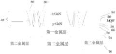
图1A至图1C为根据本发明实施例的垂直式发光二极管(VLED)晶粒10的结构示意图;其中,图1A为其剖面视图,图1B为其上视平面图,图1A为其下视平面图。如图1A至1C所示,该垂直式发光二极管晶粒10包含一第一金属12、一第二金属14、一p型半导体层16、一多重量子井(MQW)层18、及一n型半导体层20;其中,该p型半导体层16位于该第一金属12之上,该多重量子井层18位于该p型半导体层16之上,且该n型半导体层20位于该多重量子井层18之上。该垂直式发光二极管晶粒10亦包含一种子层22及一反射层24;其中,该种子层22位于该第一金属12之上,且该反射层24位于该种子层22之上。1A to 1C are schematic structural views of a vertical light emitting diode (VLED)
该p型半导体层16的较佳材料可包含p型氮化镓(p-GaN);其它适用于该p型半导体层16的材料亦包含氮化铝镓(AlGaN)、氮化铟镓(InGaN)、或氮化铟镓铝(AlInGaN)。该n型半导体层20的较佳材料可包含n型氮化镓(n-GaN);其它适用于该n型半导体层20的材料亦包含氮化铝镓(AlGaN)、氮化铟镓(InGaN)、或氮化铟镓铝(AlInGaN)。该多重量子井层18可包含一半导体材料(例如,砷化镓(GaAs)),其夹置于两层的另一半导体材料(例如,具有较宽能带间隙的砷化铝(GaAl))之间。The preferred material of the p-
该第一金属12包含互相对侧的第一表面26及第二表面28。该反射层24形成于该第一表面26之上,且该第二金属14形成于该第二表面28之上。如图1B所示,该第一金属12具有一大体上(generally)正方形(具有四个等边)的周边轮廓;或者是该第一金属12可具有任何合适的多边形周边轮廓(例如,矩形或三角形)或圆形轮廓。此外,该第一金属12的厚度及各侧边宽度分别为d1及W1。该第一金属12的代表性厚度(d1)范围为1μm至500μm;该第一金属12的代表性宽度(W1)范围为1μm至10000μm。倘若该第一金属12为圆形的轮廓,则上述的宽度(W1)可相当于该圆形的直径(D)。该第一金属12的代表性面积范围可为1μm2至10000μm2。The
该第一金属12可包含单金属层或至少二金属层的堆栈,并使用合适的沉积制程来制作。此外,该第一金属12可选用具有高导电性及高导热性的组成材料,其合适的材料包含铜(Cu)、镍(Ni)、银(Ag)、金(Au)、钴(Co)、铜-钴(Cu-Co)、镍-钴(Ni-Co)、铜-钼(Cu-Mo)、镍/铜(Ni/Cu)、镍/铜-钼(Ni/Cu-Mo)、或上述金属的合金。适用于制作该第一金属12的沉积制程包含电式沉积法(electro-deposition)、无电式沉积法(electroless-deposition)、化学气相沉积法(CVD)、电浆增强型化学气相沉积法(PECVD)、物理气相沉积法(PVD)、蒸镀法、及电浆喷涂法等。The
如图1C所示,该第二金属14具有一大体上正方形(具有四个等边)的周边轮廓,中心对称地设置于该第一金属12之上。或者是,该第二金属14可具有任何合适的多边形周边轮廓(例如,矩形或三角形),并偏移地设置于该第一金属12之上。又或者是,该第一金属12及该第二金属14可互为同心圆的圆形周边轮廓。此外,该第二金属14的厚度及各侧边宽度分别为d2及W2。该第一金属12的代表性厚度(d2)范围为1μm至500μm;该第一金属12的代表性宽度(W1)范围为0.5μm至9999μm。该第二金属14的最大宽度(W2)及面积会随着该第一金属12的最大宽度(W1)及面积而变动,但小于该第一金属12的最大宽度(W1)及面积。换言之,该第一金属12的最大宽度(W1)及面积分别大于该第二金属14的最大宽度(W2)及面积。藉此,该第一金属12及该第二金属14可形成一阶梯状保护结构。该第一金属12的面积在申请专利范围(claim)中称为「第一面积」,而该第二金属14的面积在申请专利范围(claim)中称为「第二面积」。As shown in FIG. 1C , the
该第二金属14可包含单金属层或至少二金属层的堆栈,并使用合适的沉积制程来制作。此外,该第二金属14可选用具有高导电性及高导热性的组成材料,其合适的材料包含铜(Cu)、镍(Ni)、银(Ag)、金(Au)、钴(Co)、铜-钴(Cu-Co)、镍-钴(Ni-Co)、铜-钼(Cu-Mo)、镍/铜(Ni/Cu)、镍/铜-钼(Ni/Cu-Mo)、或上述金属的合金。适用于制作该第二金属14的沉积制程包含电式沉积法(electro-deposition)、无电式沉积法(electroless-deposition)、化学气相沉积法(CVD)、电浆增强型化学气相沉积法(PECVD)、物理气相沉积法(PVD)、蒸镀法、及电浆喷涂法等。The
该种子层22可包含一使用合适沉积制程(例如,电式沉积法或无电式沉积法)制作的金属覆盖层。该种子层22用以帮助该第一金属12及该第二金属14于上述沉积制程的制作,例如,电镀法或无电式镀层法;此将详述于后。此外,该种子层22可包含单金属层或金属堆栈,其合适的材料包含Ta/Cu、Ta/TaN/Cu、TaN/Cu、Ti/TaN/Cu、Ta/TiN/Cu、Ti/Cu、Ti/Tn/Cu、TiN/Cu、Cr/Au、Cr/Au/Ni/Au、Cr/Au/Ti/Ni/Au、Ti/Au、及Ti/Ni/Au。该反射层24亦可包含单金属层或金属堆栈,其合适的材料包含Ag/Ti/Au、Ag/TiN/Cu、Ag/Ta/Au、Ag/W/Au、Ag/TaN/Cu、Ag/Ni/Au、Al/Ta/Au、Al/TaN/Cu、Ni/Ag、Ni/Al、及Ni/Ag/Ni/Au。The
该p型半导体层16、该多重量子井层18、及该n型半导体层20共同形成一磊晶堆栈30,其厚度为d且位于该种子层22之上。在该磊晶堆栈30中,该p型半导体层16及该n型半导体层20的功能为局限层,而该多重量子井层18的功能为发光层。The p-
该磊晶堆栈30可使用合适的沉积制程而形成于该反射层24之上,例如,气相磊晶法(VPE)、分子束磊晶法(MBE)、或液相磊晶法(LPE)。该磊晶堆栈30的代表性厚度(d)范围可为1μm至50μm。此外,该磊晶堆栈30具有四个倾斜的侧墙32,该等侧墙32与该种子层22表面形成一角度A;其中,该种子层22的表面平行于该第一金属12的该第一表面26。该角度A大于90度,且其代表性角度(A)范围可为100度至145度。此外,该磊晶堆栈30的形状大体上为角锥形或金字塔形,并具有一平的顶端部(而非一般角锥物具有尖的顶端部)。此外,该反射层24的面积及最大宽度可分别小于该p型半导体层16的面积及最大宽度。The
该磊晶堆栈30可具有该p型半导体层16所形成的四边基部(其宽度为W3)及该n型半导体层20所形成的四边顶端部(其宽度为W4)。该n型半导体层20的最大宽度W4小于该p型半导体层16的最大宽度W3。此外,该磊晶堆栈30的顶端部(即该n型半导体层20的顶端面)面积小于该磊晶堆栈30的基部(即该p型半导体层16的底面)面积。换言之,该磊晶堆栈30的截面积自基部至顶端部而渐减。除了角锥形的形状之外,该磊晶堆栈30亦可大体上为圆锥型的形状,其顶端部是平的,且其顶端部及基部皆为圆形。或者是,该磊晶堆栈30亦可形成长型角锥形的形状,其基部为长方形。The
图2为包含复数个垂直式发光二极管晶粒的发光二极管系统的剖面视图。请参照图2,一发光二极管(LED)34包含一基板36、该垂直式发光二极管(VLED)晶粒10、及一保护层40;其中,该垂直式发光二极管晶粒10装设于该基板36之上,该保护层40为电性绝缘且透光的材质,并密封该垂直式发光二极管晶粒10。在图2中,该发光二极管34只有一个垂直式发光二极管晶粒10装设于该基板36上;但依据实际的应用,该发光二极管34可包含复数个垂直式发光二极管晶粒10装设于该基板36上,并设置成所需要的数组型式,以形成例如发光二极管(LED)显示器的光电组件。该基板36的材质可包含半导体材料,例如,硅、砷化镓(GaAs)、碳化硅(SiC)、氮化铝(AlN)、氧化铝(Al2O3)、或蓝宝石(sapphire)等。该基板36可包含一腔体46及一背侧48;其中,该腔体46用以装设该垂直式发光二极管晶粒10于其中。一导电的晶粒黏接层(未图示)可用以将该垂直式发光二极管晶粒10黏贴于该基板36。FIG. 2 is a cross-sectional view of an LED system including a plurality of vertical LED dies. Please refer to FIG. 2, a light emitting diode (LED) 34 includes a
如图2所示,一导线38将该n型半导体层20电性连接至该基板36上的n电极42。此外,该第一金属12及该第二金属14可将该p型半导体层16电性连接至该基板36上的p电极44。该第一金属12及该第二金属14亦可提供该垂直式发光二极管晶粒10至该基板36的散热路径。该第一金属12及该第二金属14构成的阶梯状结构可进一步增强上述散热路径的散热效果。此外,该第一金属12大于该第二金属14的结构具有保护的功能,可防止晶粒黏接材料(例如,银胶或焊锡)溢出而接触到该磊晶堆栈30。As shown in FIG. 2 , a
请参照图3A至图3K,其为该垂直式发光二极管(VLED)晶粒10制作方法的步骤示意图。首先,如图3A所示,提供一承载基板50。该承载基板50可以是晶圆的形式,其材质可为例如蓝宝石、碳化硅(SiC)、硅、锗(Ge)、氧化锌(ZnO)、或砷化镓(GaAs)。在本实施例中,该承载基板50为蓝宝石基板。Please refer to FIG. 3A to FIG. 3K , which are schematic diagrams showing steps of the method for manufacturing the vertical light emitting diode (VLED) die 10 . First, as shown in FIG. 3A , a
如图3A所示,可使用合适的沉积制程而形成一多层磊晶结构52A于该承载基板50上,例如,气相磊晶法(VPE)、分子束磊晶法(MBE)、或液相磊晶法(LPE)。该多层磊晶结构52A可包含一n型层54、至少一量子井层56、及一p型层58。在本实施例中,该n型层54包含n型氮化镓(n-GaN)且该p型层58包含p型氮化镓(p-GaN)。除了氮化镓之外,该n型层54及该p型层58亦可包含其它各种的复合物半导体层材料,例如,氮化铝镓(AlGaN)、氮化铟镓(InGaN)、或氮化铟镓铝(AlInGaN)。该等量子井层56的材质可为合适的材料,例如,砷化镓(GaAs)层,其夹置于两层的另一材料(例如,具有较宽能带间隙的砷化铝(GaAl))之间。As shown in FIG. 3A , a multilayer epitaxial structure 52A can be formed on the
接着如图3B所示,可使用合适的制程来形成贯穿该多层磊晶结构52A的凹槽62,该等凹槽62的底端可在该承载基板50上,或是延伸入该承载基板50一小段距离。该等凹槽62可形成十字形图案,类似传统半导体制程的晶粒之间的分隔道,使得复数个晶粒60可被界定出,并用以分开该磊晶堆栈52。上述的合适制程可包含藉由硬式屏蔽(hard mask)的干式蚀刻法。此外,雷射切割法、刀锯切割法、钻石切割法、湿式蚀刻法、及冲水法(water jetting)亦为其它合适的制程。在本凹槽制作步骤之后,该等晶粒60可以液体或溶剂清洗,藉以去除该蚀刻屏蔽或其它的保护涂层。该等凹槽62的宽度w范围约为0.1μm至300μm。Next, as shown in FIG. 3B , a suitable process can be used to form
此外,如图3B所示,可使用合适的制程以于该p型层58之上形成一反射层66,其功能为反射器或反射镜以反射该垂直式发光二极管晶粒10的发光。举例而言,该反射层66可包含多层金属,例如,Ni/Ag/Ni/Au、Ag/Ni/Au、Ti/Ag/Ni/Au、Ag/Pt、Ag/Pd、或Ag/Cr,其可藉由沉积含有银(Ag)、金(Au)、铬(Cr)、铂(Pt)、铅(Pd)、或铝(Al)的合金而形成。该反射层(反射镜)66的厚度可小于约1.0μm。该反射层66的高温退火或合金化可用来改善其接触电阻及其对于该p型层58的黏着性。例如,上述的退火或合金化制程可在至少150℃的温度及惰性的环境(例如,含少量或完全无氧、氢、或氧氢皆无的气体环境)下进行。In addition, as shown in FIG. 3B , a
接着如图3C所示,一种子层72可使用电镀法或无电式镀层法而形成于该反射层66上以及该等凹槽62的侧墙上。该种子层72可包含单一层或多层堆栈,例如,Ta/Cu、Ta/TaN/Cu、TaN/Cu、Ti/TaN/Cu、Ta/TiN/Cu、Ti/Cu、Ti/Tn/Cu、TiN/Cu、Ti/Cu、Ti/Tn/Cu、TiN/Cu、Cr/Au、Cr/Au/Ni/Au、Cr/Au/Ti/Ni/Au、Ti/Au、Ti/Ni/Au、Ni/Au、或Ni/Cu。该反射层66亦可形成一覆盖层,其亦可具有种子层的功能。在本实施例中,该反射层66可包含单一层或多层堆栈,例如,Ag/Ti/Au、Ag/TiN/Cu、Ag/Ta/Au、Ag/W/Au、Ag/TaN/Cu、Al/Ta/Au、Al/TaN/Cu、Ni/Ag、Ni/Al、或Ni/Ag/Ni/Au。Next, as shown in FIG. 3C , a
接着如图3D及图3E所示,一厚度d1的第一金属层74沉积于该种子层72上,且一厚度d2的第二金属层76沉积于该第一金属层74上。该第一金属层74将形成如图1A之该第一金属12,且该第二金属层76将形成如图1A的该第二金属14。该第一金属层74可使用合适的沉积制程来制作,例如,电式沉积法(electro-deposition)或无电式沉积法(electroless-deposition),以达到所需的厚度d1。该第一金属层74的代表性厚度(d1)范围为1μm至500μm。类似地,该第二金属层76可使用合适的沉积制程来制作,例如,电式沉积法或无电式沉积法,以达到所需的厚度d2。该第二金属层76的代表性厚度(d2)范围为1μm至500μm。该第一金属层74及该第二金属层76可包含单层的金属(例如,铜(Cu)、镍(Ni)、银(Ag)、金(Au)、或钴(Co))、金属合金(例如,铜-钴(Cu-Co)或铜-钼(Cu-Mo))、或金属层堆栈(例如,镍/铜(Ni/Cu)或镍/铜-钼(Ni/Cu-Mo))。其它适用于制作该第一金属层74及该第二金属层76的沉积制程包含化学气相沉积法(CVD)、电浆增强型化学气相沉积法(PECVD)、物理气相沉积法(PVD)、蒸镀法、及电浆喷涂法等。Next, as shown in FIGS. 3D and 3E , a
接着如图3E所示,该第二金属层76可使用合适的制程加以图案化,例如,对原本沉积的层膜进行蚀刻(例如,减法制程)或藉由屏蔽的图案化沉积(例如,加法制程),以定义出该第二金属14的形状。该第二金属层76的图案化制程将使得该第二金属14的面积及宽度W2分别小于该第一金属12的面积及宽度W1。此外,一或多个额外的金属层(例如,Cr/Au、Ni或Ni/Au,未图示)可形成于该第二金属层76上以及该第一金属层74的外露面上,藉以防止氧化与腐蚀。Next, as shown in FIG. 3E , the
接着如图3F所示,该承载基板50可使用合适的制程而自该n型层54上移除,例如,脉冲式雷射照射法、蚀刻法、或化学机械平坦化制程(ChemicalMechanical planarization,CMP)。Then, as shown in FIG. 3F, the
接着如图3G所示,一硬式屏蔽78可形成于该承载基板50移除后的该n型层54表面上。该硬式屏蔽78可包含例如氧化硅(SiO2)或氮化硅(Si3N4)的沉积材料。该硬式屏蔽78亦可包含有机聚合物材料,例如,环氧化物(epoxy)、聚亚酰氨(polyimide)、热塑材料或溶胶-凝胶(sol-gel)材料。该硬式屏蔽78亦可采用光敏有机材料,例如,SU-8、NR-7、或AZ5214E。或者是,该硬式屏蔽78可包含无机材料,例如,氧化硅(SiO2)、氧化锌(ZnO)、氧化钽(Ta2O5)、氧化钛(TiO2)、氧化铪(HfO)、或氧化镁(MgO)。Next, as shown in FIG. 3G , a
接着如图3H所示,该硬式屏蔽78可用以蚀刻出复数个凹槽80,其贯穿该磊晶堆栈52而至该种子层72。所使用的蚀刻制程可包含干式蚀刻(ICP RIE)、湿式化学蚀刻、或光增强式化学蚀刻。此外,邻近该n型层54表面的该等凹槽80尺寸可大于邻近该p型层58表面的该等凹槽80尺寸。换言之,该等凹槽80的尺寸随着其深度的增加而减小。该等凹槽80的倾斜度加上90度将会等于如图1A所示的该垂直式发光二极管晶粒10的该磊晶堆栈的角度A。Next, as shown in FIG. 3H , the
接着如图3I所示,该硬式屏蔽78可使用合适的溶剂或使用合适的干式或湿式蚀刻制程而移除。The
接着如图3J所示,可进行晶粒分割制程,以将该等晶粒60分割成个别的垂直式发光二极管(VLED)10。此分割制程可使用合适的制作方法,例如,雷射切割法、刀锯切割法、折断法(breaking)、空气刀法(air knifing)、或冲水法(waterjetting)。此外,一或多个抗氧化层(未图示)可使用合适的制作方法而铺涂于特定的表面(例如,边侧区),例如,使用冲水法溶液的镀膜法。Next, as shown in FIG. 3J , a die separation process may be performed to divide the die 60 into individual vertical light emitting diodes (VLEDs) 10 . A suitable manufacturing method can be used for the dividing process, for example, laser cutting, saw cutting, breaking, air knife, or waterjetting. In addition, one or more anti-oxidation layers (not shown) can be applied to a specific surface (eg, side area) using a suitable fabrication method, eg, coating using a flushing solution.
如图3K所示,各个垂直式发光二极管(VLED)10包含一第一金属12、一第二金属14、一p型半导体层16、一多重量子井(MQW)层18、及一n型半导体层20;其中,部分的该第一金属层74形成该第一金属12(如图3J所示);部分的该第二金属层76形成该第二金属14(如图3J所示);部分的该p型层58形成该p型半导体层16(如图3J所示);部分的该多重量子井层58形成该多重量子井(MQW)层18(如图3J所示);且部分的该n型层54形成该n型半导体层20(如图3J所示)。各个垂直式发光二极管(VLED)10亦包含一种子层22及一反射层24;其中,部分的该种子层72形成该种子层22(如图3J所示),且部分的该反射层66形成该反射层24(如图3J所示)。As shown in Figure 3K, each vertical light emitting diode (VLED) 10 includes a
以上所描述者即为本发明实施例的垂直式发光二极管(VLED)晶粒及其制作方法。What has been described above is the vertical light emitting diode (VLED) chip and the manufacturing method thereof according to the embodiment of the present invention.
以上这些实施例仅是范例性的,并不对本发明的范围构成任何限制。本领域技术人员应该理解的是,在不偏离本发明的精神和范围下可以对本发明技术方案的细节和形式进行修改或替换,但这些修改和替换均落入本发明的保护范围内。The above embodiments are only exemplary, and do not constitute any limitation to the scope of the present invention. Those skilled in the art should understand that the details and forms of the technical solutions of the present invention can be modified or replaced without departing from the spirit and scope of the present invention, but these modifications and replacements all fall within the protection scope of the present invention.
Claims (20)
Translated fromChineseApplications Claiming Priority (2)
| Application Number | Priority Date | Filing Date | Title |
|---|---|---|---|
| US13/325,376US8686461B2 (en) | 2011-01-03 | 2011-12-14 | Light emitting diode (LED) die having stepped substrates and method of fabrication |
| US13/325376 | 2011-12-14 |
Publications (1)
| Publication Number | Publication Date |
|---|---|
| CN103165806Atrue CN103165806A (en) | 2013-06-19 |
Family
ID=48588716
Family Applications (1)
| Application Number | Title | Priority Date | Filing Date |
|---|---|---|---|
| CN2012102526830APendingCN103165806A (en) | 2011-12-14 | 2012-07-20 | Vertical light-emitting diode crystal grain and manufacturing method thereof |
Country Status (6)
| Country | Link |
|---|---|
| US (2) | US8686461B2 (en) |
| JP (1) | JP2013125961A (en) |
| KR (1) | KR20130069351A (en) |
| CN (1) | CN103165806A (en) |
| TW (1) | TWI479685B (en) |
| WO (1) | WO2013086781A1 (en) |
Cited By (2)
| Publication number | Priority date | Publication date | Assignee | Title |
|---|---|---|---|---|
| CN104393140A (en)* | 2014-11-06 | 2015-03-04 | 中国科学院半导体研究所 | High-reflectiveness vertical structure light emitting diode chip and preparation method thereof |
| CN113016079A (en)* | 2019-10-18 | 2021-06-22 | 深圳市大疆创新科技有限公司 | Semiconductor chip packaging structure, packaging method and electronic equipment |
Families Citing this family (18)
| Publication number | Priority date | Publication date | Assignee | Title |
|---|---|---|---|---|
| US8933467B2 (en) | 2009-08-13 | 2015-01-13 | SemiLEDs Optoelectronics Co., Ltd. | Smart integrated semiconductor light emitting system including nitride based light emitting diodes (LED) and application specific integrated circuits (ASIC) |
| US9214456B2 (en) | 2009-08-13 | 2015-12-15 | SemiLEDs Optoelectronics Co., Ltd. | Light emitting diode (LED) system having lighting device and wireless control system |
| US8686461B2 (en) | 2011-01-03 | 2014-04-01 | SemiLEDs Optoelectronics Co., Ltd. | Light emitting diode (LED) die having stepped substrates and method of fabrication |
| US8835945B2 (en)* | 2013-01-11 | 2014-09-16 | Lighting Science Group Corporation | Serially-connected light emitting diodes, methods of forming same, and luminaires containing same |
| KR101887942B1 (en)* | 2012-05-07 | 2018-08-14 | 삼성전자주식회사 | Light emitting device |
| CN102903813B (en)* | 2012-09-29 | 2014-04-02 | 海迪科(南通)光电科技有限公司 | Fabrication method of high-voltage LED device with integrated graphic array |
| US20140151630A1 (en)* | 2012-12-04 | 2014-06-05 | Feng-Hsu Fan | Protection for the epitaxial structure of metal devices |
| JP2014154693A (en)* | 2013-02-08 | 2014-08-25 | Toyoda Gosei Co Ltd | Group iii nitride semiconductor light-emitting element and manufacturing method of the same |
| JP2015115538A (en)* | 2013-12-13 | 2015-06-22 | 株式会社東京精密 | Wafer processing method |
| US10217914B2 (en) | 2015-05-27 | 2019-02-26 | Samsung Electronics Co., Ltd. | Semiconductor light emitting device |
| JP6591254B2 (en)* | 2015-10-16 | 2019-10-16 | スタンレー電気株式会社 | Semiconductor light emitting device and method for manufacturing semiconductor light emitting device |
| KR102474502B1 (en) | 2016-08-01 | 2022-12-08 | 주식회사 클랩 | Sheet lighting and manufacturing method of the same |
| KR20180023881A (en) | 2016-08-26 | 2018-03-07 | 김영범 | Sheet lighting and manufacturing method of the same |
| KR102711807B1 (en) | 2016-08-29 | 2024-09-30 | 김영범 | Display panel and manufacturing method of the same |
| KR102464391B1 (en) | 2016-09-22 | 2022-11-08 | 주식회사 클랩 | Sheet lighting and manufacturing method of the same |
| DE102018101393A1 (en)* | 2018-01-23 | 2019-07-25 | Osram Opto Semiconductors Gmbh | OPTOELECTRONIC SEMICONDUCTOR CHIP AND METHOD FOR PRODUCING AN OPTOELECTRONIC SEMICONDUCTOR CHIP |
| WO2020251078A1 (en)* | 2019-06-12 | 2020-12-17 | 서울바이오시스 주식회사 | Light-emitting stack and display device including same |
| KR102766110B1 (en)* | 2022-02-25 | 2025-02-12 | 고려대학교 산학협력단 | Vertical alignment assembly of light emitting device and method of vertically aligning light emitting device |
Citations (3)
| Publication number | Priority date | Publication date | Assignee | Title |
|---|---|---|---|---|
| CN1577904A (en)* | 2003-07-25 | 2005-02-09 | 夏普株式会社 | Nitride-based compound semiconductor light-emitting device and method of fabricating the same |
| US20110220933A1 (en)* | 2010-03-09 | 2011-09-15 | Kabushiki Kaisha Toshiba | Semiconductor light emitting device and method of fabricating semiconductor light emitting device |
| US20110227121A1 (en)* | 2010-03-19 | 2011-09-22 | Yuko Kato | Semiconductor light emmiting device |
Family Cites Families (35)
| Publication number | Priority date | Publication date | Assignee | Title |
|---|---|---|---|---|
| US6803243B2 (en)* | 2001-03-15 | 2004-10-12 | Cree, Inc. | Low temperature formation of backside ohmic contacts for vertical devices |
| US6703290B2 (en) | 1999-07-14 | 2004-03-09 | Seh America, Inc. | Growth of epitaxial semiconductor material with improved crystallographic properties |
| EP1104031B1 (en) | 1999-11-15 | 2012-04-11 | Panasonic Corporation | Nitride semiconductor laser diode and method of fabricating the same |
| DE10112542B9 (en)* | 2001-03-15 | 2013-01-03 | Osram Opto Semiconductors Gmbh | Radiation-emitting optical component |
| WO2004068572A2 (en)* | 2003-01-31 | 2004-08-12 | Osram Opto Semiconductors Gmbh | Method for producing a semiconductor component |
| TW200616254A (en)* | 2004-11-12 | 2006-05-16 | Univ Nat Central | Light emitting diode structure and manufacturing method thereof |
| US7473936B2 (en) | 2005-01-11 | 2009-01-06 | Semileds Corporation | Light emitting diodes (LEDs) with improved light extraction by roughening |
| US7432119B2 (en) | 2005-01-11 | 2008-10-07 | Semileds Corporation | Light emitting diode with conducting metal substrate |
| US8685764B2 (en) | 2005-01-11 | 2014-04-01 | SemiLEDs Optoelectronics Co., Ltd. | Method to make low resistance contact |
| US7186580B2 (en) | 2005-01-11 | 2007-03-06 | Semileds Corporation | Light emitting diodes (LEDs) with improved light extraction by roughening |
| US7524686B2 (en) | 2005-01-11 | 2009-04-28 | Semileds Corporation | Method of making light emitting diodes (LEDs) with improved light extraction by roughening |
| US7378288B2 (en) | 2005-01-11 | 2008-05-27 | Semileds Corporation | Systems and methods for producing light emitting diode array |
| US7646033B2 (en) | 2005-01-11 | 2010-01-12 | Semileds Corporation | Systems and methods for producing white-light light emitting diodes |
| US7195944B2 (en) | 2005-01-11 | 2007-03-27 | Semileds Corporation | Systems and methods for producing white-light emitting diodes |
| US7563625B2 (en) | 2005-01-11 | 2009-07-21 | SemiLEDs Optoelectronics Co., Ltd. | Method of making light-emitting diodes (LEDs) with improved light extraction by roughening |
| JP2007096079A (en)* | 2005-09-29 | 2007-04-12 | Stanley Electric Co Ltd | Semiconductor light emitting device |
| US7723718B1 (en) | 2005-10-11 | 2010-05-25 | SemiLEDs Optoelectronics Co., Ltd. | Epitaxial structure for metal devices |
| US7968379B2 (en)* | 2006-03-09 | 2011-06-28 | SemiLEDs Optoelectronics Co., Ltd. | Method of separating semiconductor dies |
| US7615789B2 (en) | 2006-05-09 | 2009-11-10 | SemiLEDs Optoelectronics Co., Ltd. | Vertical light emitting diode device structure |
| US7829440B2 (en) | 2006-08-07 | 2010-11-09 | Semileds Optoelectronics Co. Ltd. | Method of separating semiconductor dies |
| US7892891B2 (en) | 2006-10-11 | 2011-02-22 | SemiLEDs Optoelectronics Co., Ltd. | Die separation |
| US20080087875A1 (en) | 2006-10-11 | 2008-04-17 | Feng-Hsu Fan | Protection for the epitaxial structure of metal devices |
| US7781247B2 (en) | 2006-10-26 | 2010-08-24 | SemiLEDs Optoelectronics Co., Ltd. | Method for producing Group III-Group V vertical light-emitting diodes |
| US7811842B2 (en) | 2007-01-11 | 2010-10-12 | SemiLEDs Optoelectronics Co., Ltd. | LED array |
| US7781783B2 (en) | 2007-02-07 | 2010-08-24 | SemiLEDs Optoelectronics Co., Ltd. | White light LED device |
| US7759146B2 (en) | 2007-05-04 | 2010-07-20 | SemiLEDs Optoelectronics Co., Ltd. | Method of making high efficiency UV VLED on metal substrate |
| US7759670B2 (en) | 2007-06-12 | 2010-07-20 | SemiLEDs Optoelectronics Co., Ltd. | Vertical LED with current guiding structure |
| TWI411124B (en)* | 2007-07-10 | 2013-10-01 | Delta Electronics Inc | Light-emitting diode device and method of manufacturing same |
| US8829554B2 (en)* | 2008-04-02 | 2014-09-09 | Lg Innotek Co., Ltd. | Light emitting element and a production method therefor |
| JP2009283912A (en)* | 2008-04-25 | 2009-12-03 | Sanyo Electric Co Ltd | Nitride-based semiconductor device and method of manufacturing the same |
| JP5057398B2 (en)* | 2008-08-05 | 2012-10-24 | シャープ株式会社 | Nitride semiconductor light emitting device and manufacturing method thereof |
| KR101039904B1 (en)* | 2010-01-15 | 2011-06-09 | 엘지이노텍 주식회사 | Light emitting device, light emitting device package and manufacturing method |
| US8105852B2 (en) | 2010-01-15 | 2012-01-31 | Koninklijke Philips Electronics N.V. | Method of forming a composite substrate and growing a III-V light emitting device over the composite substrate |
| US8686461B2 (en)* | 2011-01-03 | 2014-04-01 | SemiLEDs Optoelectronics Co., Ltd. | Light emitting diode (LED) die having stepped substrates and method of fabrication |
| US20120168714A1 (en) | 2011-01-03 | 2012-07-05 | SemiLEDs Optoelectronics Co., Ltd. | Vertical light emitting diode (vled) die and method of fabrication |
- 2011
- 2011-12-14USUS13/325,376patent/US8686461B2/enactiveActive
- 2012
- 2012-06-29TWTW101123435Apatent/TWI479685B/enactive
- 2012-07-20CNCN2012102526830Apatent/CN103165806A/enactivePending
- 2012-07-26JPJP2012165474Apatent/JP2013125961A/enactivePending
- 2012-10-16KRKR1020120114802Apatent/KR20130069351A/ennot_activeCeased
- 2012-11-23WOPCT/CN2012/001576patent/WO2013086781A1/enactiveApplication Filing
- 2014
- 2014-02-07USUS14/175,033patent/US9343620B2/enactiveActive
Patent Citations (3)
| Publication number | Priority date | Publication date | Assignee | Title |
|---|---|---|---|---|
| CN1577904A (en)* | 2003-07-25 | 2005-02-09 | 夏普株式会社 | Nitride-based compound semiconductor light-emitting device and method of fabricating the same |
| US20110220933A1 (en)* | 2010-03-09 | 2011-09-15 | Kabushiki Kaisha Toshiba | Semiconductor light emitting device and method of fabricating semiconductor light emitting device |
| US20110227121A1 (en)* | 2010-03-19 | 2011-09-22 | Yuko Kato | Semiconductor light emmiting device |
Cited By (3)
| Publication number | Priority date | Publication date | Assignee | Title |
|---|---|---|---|---|
| CN104393140A (en)* | 2014-11-06 | 2015-03-04 | 中国科学院半导体研究所 | High-reflectiveness vertical structure light emitting diode chip and preparation method thereof |
| CN113016079A (en)* | 2019-10-18 | 2021-06-22 | 深圳市大疆创新科技有限公司 | Semiconductor chip packaging structure, packaging method and electronic equipment |
| CN113016079B (en)* | 2019-10-18 | 2022-06-24 | 深圳市大疆创新科技有限公司 | Semiconductor chip packaging structure, packaging method and electronic device |
Also Published As
| Publication number | Publication date |
|---|---|
| US20140151635A1 (en) | 2014-06-05 |
| US8686461B2 (en) | 2014-04-01 |
| US20120168716A1 (en) | 2012-07-05 |
| TW201324845A (en) | 2013-06-16 |
| KR20130069351A (en) | 2013-06-26 |
| JP2013125961A (en) | 2013-06-24 |
| US9343620B2 (en) | 2016-05-17 |
| WO2013086781A1 (en) | 2013-06-20 |
| TWI479685B (en) | 2015-04-01 |
Similar Documents
| Publication | Publication Date | Title |
|---|---|---|
| TWI479685B (en) | Vertical light-emitting diode crystal grain and manufacturing method thereof | |
| TWI606614B (en) | Vertical light emitting diode crystal grain and manufacturing method thereof | |
| KR101396121B1 (en) | Method for handling a semiconductor wafer assembly | |
| US7432119B2 (en) | Light emitting diode with conducting metal substrate | |
| US20060154393A1 (en) | Systems and methods for removing operating heat from a light emitting diode | |
| US8759128B2 (en) | Light emitting diode (LED) die having recessed electrode and light extraction structures and method of fabrication | |
| US20080194051A1 (en) | Die separation | |
| US9437794B2 (en) | Method of fabricating a flip chip light emitting diode (FCLED) die having N-conductor layer | |
| CN103794686B (en) | Light emitting semiconductor device and its manufacturing method | |
| US9059377B2 (en) | Solid state lighting devices with low contact resistance and methods of manufacturing | |
| EP3143648A1 (en) | Method of forming a light-emitting device | |
| KR101364167B1 (en) | Vertical light emitting diode and method of fabricating the same | |
| CN101740674A (en) | Light-emitting element structure and manufacturing method thereof | |
| KR101316121B1 (en) | Method of fabricating vertical light emitting diode | |
| KR101158077B1 (en) | High efficiency light emitting diode and method of fabricating the same | |
| KR101634370B1 (en) | High efficiency light emitting diode and method of fabricating the same | |
| KR20110121176A (en) | Semiconductor light emitting device and manufacturing method thereof | |
| KR100832301B1 (en) | Semiconductor light emitting device with surface irregularities on the same substrate and its manufacturing method | |
| TWI336142B (en) | Light-emitting diode and manufacturing method thereof | |
| KR20120033294A (en) | High efficiency light emitting diode and method of fabricating the same |
Legal Events
| Date | Code | Title | Description |
|---|---|---|---|
| C06 | Publication | ||
| PB01 | Publication | ||
| C10 | Entry into substantive examination | ||
| SE01 | Entry into force of request for substantive examination | ||
| C02 | Deemed withdrawal of patent application after publication (patent law 2001) | ||
| WD01 | Invention patent application deemed withdrawn after publication | Application publication date:20130619 |