CN103155024A - Solid state light emitting device and signage with photoluminescence wavelength conversion - Google Patents
Solid state light emitting device and signage with photoluminescence wavelength conversionDownload PDFInfo
- Publication number
- CN103155024A CN103155024ACN2011800483035ACN201180048303ACN103155024ACN 103155024 ACN103155024 ACN 103155024ACN 2011800483035 ACN2011800483035 ACN 2011800483035ACN 201180048303 ACN201180048303 ACN 201180048303ACN 103155024 ACN103155024 ACN 103155024A
- Authority
- CN
- China
- Prior art keywords
- light
- phosphor
- emitting device
- reflecting material
- light reflecting
- Prior art date
- Legal status (The legal status is an assumption and is not a legal conclusion. Google has not performed a legal analysis and makes no representation as to the accuracy of the status listed.)
- Granted
Links
Images


Classifications
- F—MECHANICAL ENGINEERING; LIGHTING; HEATING; WEAPONS; BLASTING
- F21—LIGHTING
- F21K—NON-ELECTRIC LIGHT SOURCES USING LUMINESCENCE; LIGHT SOURCES USING ELECTROCHEMILUMINESCENCE; LIGHT SOURCES USING CHARGES OF COMBUSTIBLE MATERIAL; LIGHT SOURCES USING SEMICONDUCTOR DEVICES AS LIGHT-GENERATING ELEMENTS; LIGHT SOURCES NOT OTHERWISE PROVIDED FOR
- F21K9/00—Light sources using semiconductor devices as light-generating elements, e.g. using light-emitting diodes [LED] or lasers
- F21K9/20—Light sources comprising attachment means
- F21K9/23—Retrofit light sources for lighting devices with a single fitting for each light source, e.g. for substitution of incandescent lamps with bayonet or threaded fittings
- F21K9/232—Retrofit light sources for lighting devices with a single fitting for each light source, e.g. for substitution of incandescent lamps with bayonet or threaded fittings specially adapted for generating an essentially omnidirectional light distribution, e.g. with a glass bulb
- F—MECHANICAL ENGINEERING; LIGHTING; HEATING; WEAPONS; BLASTING
- F21—LIGHTING
- F21K—NON-ELECTRIC LIGHT SOURCES USING LUMINESCENCE; LIGHT SOURCES USING ELECTROCHEMILUMINESCENCE; LIGHT SOURCES USING CHARGES OF COMBUSTIBLE MATERIAL; LIGHT SOURCES USING SEMICONDUCTOR DEVICES AS LIGHT-GENERATING ELEMENTS; LIGHT SOURCES NOT OTHERWISE PROVIDED FOR
- F21K9/00—Light sources using semiconductor devices as light-generating elements, e.g. using light-emitting diodes [LED] or lasers
- F21K9/60—Optical arrangements integrated in the light source, e.g. for improving the colour rendering index or the light extraction
- F21K9/64—Optical arrangements integrated in the light source, e.g. for improving the colour rendering index or the light extraction using wavelength conversion means distinct or spaced from the light-generating element, e.g. a remote phosphor layer
- H—ELECTRICITY
- H10—SEMICONDUCTOR DEVICES; ELECTRIC SOLID-STATE DEVICES NOT OTHERWISE PROVIDED FOR
- H10H—INORGANIC LIGHT-EMITTING SEMICONDUCTOR DEVICES HAVING POTENTIAL BARRIERS
- H10H20/00—Individual inorganic light-emitting semiconductor devices having potential barriers, e.g. light-emitting diodes [LED]
- H10H20/80—Constructional details
- H10H20/85—Packages
- H10H20/851—Wavelength conversion means
- H10H20/8511—Wavelength conversion means characterised by their material, e.g. binder
- H10H20/8512—Wavelength conversion materials
- H10H20/8513—Wavelength conversion materials having two or more wavelength conversion materials
- H—ELECTRICITY
- H10—SEMICONDUCTOR DEVICES; ELECTRIC SOLID-STATE DEVICES NOT OTHERWISE PROVIDED FOR
- H10H—INORGANIC LIGHT-EMITTING SEMICONDUCTOR DEVICES HAVING POTENTIAL BARRIERS
- H10H20/00—Individual inorganic light-emitting semiconductor devices having potential barriers, e.g. light-emitting diodes [LED]
- H10H20/80—Constructional details
- H10H20/85—Packages
- H10H20/851—Wavelength conversion means
- H10H20/8515—Wavelength conversion means not being in contact with the bodies
- H—ELECTRICITY
- H10—SEMICONDUCTOR DEVICES; ELECTRIC SOLID-STATE DEVICES NOT OTHERWISE PROVIDED FOR
- H10H—INORGANIC LIGHT-EMITTING SEMICONDUCTOR DEVICES HAVING POTENTIAL BARRIERS
- H10H20/00—Individual inorganic light-emitting semiconductor devices having potential barriers, e.g. light-emitting diodes [LED]
- H10H20/80—Constructional details
- H10H20/882—Scattering means
- F—MECHANICAL ENGINEERING; LIGHTING; HEATING; WEAPONS; BLASTING
- F21—LIGHTING
- F21V—FUNCTIONAL FEATURES OR DETAILS OF LIGHTING DEVICES OR SYSTEMS THEREOF; STRUCTURAL COMBINATIONS OF LIGHTING DEVICES WITH OTHER ARTICLES, NOT OTHERWISE PROVIDED FOR
- F21V3/00—Globes; Bowls; Cover glasses
- F21V3/04—Globes; Bowls; Cover glasses characterised by materials, surface treatments or coatings
- F21V3/06—Globes; Bowls; Cover glasses characterised by materials, surface treatments or coatings characterised by the material
- F21V3/061—Globes; Bowls; Cover glasses characterised by materials, surface treatments or coatings characterised by the material the material being glass
- F—MECHANICAL ENGINEERING; LIGHTING; HEATING; WEAPONS; BLASTING
- F21—LIGHTING
- F21V—FUNCTIONAL FEATURES OR DETAILS OF LIGHTING DEVICES OR SYSTEMS THEREOF; STRUCTURAL COMBINATIONS OF LIGHTING DEVICES WITH OTHER ARTICLES, NOT OTHERWISE PROVIDED FOR
- F21V3/00—Globes; Bowls; Cover glasses
- F21V3/04—Globes; Bowls; Cover glasses characterised by materials, surface treatments or coatings
- F21V3/06—Globes; Bowls; Cover glasses characterised by materials, surface treatments or coatings characterised by the material
- F21V3/062—Globes; Bowls; Cover glasses characterised by materials, surface treatments or coatings characterised by the material the material being plastics
- F—MECHANICAL ENGINEERING; LIGHTING; HEATING; WEAPONS; BLASTING
- F21—LIGHTING
- F21Y—INDEXING SCHEME ASSOCIATED WITH SUBCLASSES F21K, F21L, F21S and F21V, RELATING TO THE FORM OR THE KIND OF THE LIGHT SOURCES OR OF THE COLOUR OF THE LIGHT EMITTED
- F21Y2115/00—Light-generating elements of semiconductor light sources
- F21Y2115/10—Light-emitting diodes [LED]
- F—MECHANICAL ENGINEERING; LIGHTING; HEATING; WEAPONS; BLASTING
- F21—LIGHTING
- F21Y—INDEXING SCHEME ASSOCIATED WITH SUBCLASSES F21K, F21L, F21S and F21V, RELATING TO THE FORM OR THE KIND OF THE LIGHT SOURCES OR OF THE COLOUR OF THE LIGHT EMITTED
- F21Y2115/00—Light-generating elements of semiconductor light sources
- F21Y2115/30—Semiconductor lasers
Landscapes
- Engineering & Computer Science (AREA)
- General Engineering & Computer Science (AREA)
- Physics & Mathematics (AREA)
- Microelectronics & Electronic Packaging (AREA)
- Optics & Photonics (AREA)
- Led Device Packages (AREA)
- Luminescent Compositions (AREA)
- Planar Illumination Modules (AREA)
Abstract
Description
Translated fromChinese技术领域technical field
本发明的一些实施例涉及固态发光装置及标牌,其使用光致发光波长转换,以将由固态发光体产生的光转换为期望色彩的光。Some embodiments of the invention relate to solid state light emitting devices and signs that use photoluminescence wavelength conversion to convert light generated by solid state light emitters into light of a desired color.
背景技术Background technique
所属技术领域已知白色发光LED(“白色LED”),且是相对较新近的创新。由于其较长的操作寿命期望值(>50,000小时)及较高的发光效率(每瓦特70流明及更高),越来越多高亮度白色LED用于代替常规荧光光源、小型荧光光源及白炽光源。White light emitting LEDs ("white LEDs") are known in the art and are a relatively recent innovation. Due to their long operating life expectancy (>50,000 hours) and high luminous efficiency (70 lumens per watt and higher), more and more high-brightness white LEDs are used to replace conventional fluorescent light sources, compact fluorescent light sources, and incandescent light sources .
直到开发出在电磁光谱的蓝色/紫外线部分中发射的LED,开发基于LED的白光源才变得实际。如在例如US5,998,925中所教示,白色LED包含一种或一种以上光致发光材料(例如,磷光体材料),其吸收由所述LED发射的一部分辐射,且重新发射不同色彩(波长)的辐射。通常,LED芯片或裸片产生蓝光,且所述磷光体吸收某个百分比的蓝光,且重新发射黄光或绿光及红光、绿光及黄光、绿光及橙光或黄光及红光的组合。由所述LED产生的未被所述磷光体吸收的蓝光部分与由所述磷光体发射的光组合,提供对于人眼呈现为接近白色的光。It was not practical to develop LED-based white light sources until LEDs were developed that emit in the blue/ultraviolet portion of the electromagnetic spectrum. As taught in, for example, US 5,998,925, white LEDs comprise one or more photoluminescent materials (eg, phosphor materials) that absorb a portion of the radiation emitted by the LED and re-emit a different color (wavelength) radiation. Typically, the LED chip or die produces blue light and the phosphor absorbs some percentage of the blue light and re-emits yellow or green and red, green and yellow, green and orange or yellow and red Combination of light. The portion of the blue light produced by the LED that is not absorbed by the phosphor combines with the light emitted by the phosphor to provide light that appears nearly white to the human eye.
由所述LED光产生的确切色彩在很大程度上取决于由所述磷光体材料发射的光的量,因为所述磷光体发射的光的量(及波长)及残余的蓝光的量(及波长)的组合决定所得光的色彩。因此,用来产生白光的基于磷光体的LED装置将需要足够量的磷光体以正确运作,因为不具有足够量的磷光体材料的所述基于磷光体的LED装置将无法产生呈现为白色的光。The exact color produced by the LED light depends largely on the amount of light emitted by the phosphor material, since the amount (and wavelength) of light emitted by the phosphor and the amount of residual blue light (and wavelength) determines the color of the resulting light. Accordingly, a phosphor-based LED device used to produce white light will require a sufficient amount of phosphor to function properly, as such a phosphor-based LED device without a sufficient amount of phosphor material will not be able to produce light that appears white .
问题在于磷光体材料相对昂贵,且因此对应于生产基于磷光体的LED装置的成本的主要部分。通常,在LED灯中的磷光体材料与光透射材料(例如硅酮或环氧树脂材料)混合,且所述混合物直接施覆到所述LED裸片的发光表面。此导致直接置于所述LED裸片上的磷光体材料的较小覆盖面积层,但其在生产上仍然较昂贵,部分是因为所述磷光体材料的高昂成本。The problem is that phosphor materials are relatively expensive and thus represent a major part of the cost of producing phosphor-based LED devices. Typically, the phosphor material in an LED lamp is mixed with a light transmissive material, such as a silicone or epoxy material, and the mixture is applied directly to the light emitting surface of the LED die. This results in a smaller footprint layer of phosphor material placed directly on the LED die, but it is still more expensive to produce, in part because of the high cost of the phosphor material.
如颁予Li的第US2008/02118992A1号美国专利申请案中所揭示,还已知将所述磷光体材料作为光学组件上的一层而提供,或将所述磷光体材料合并在光学组件内,所述光学组件在物理上位于所述LED裸片远程。此通常导致具有比前述段落中描述的方法大很多的覆盖面积的一层磷光体材料。因为其较大尺寸,通常需要更大量的磷光体,以制造此些“远程磷光体”LED装置。结果,为提供此些远程磷光体LED装置需要的增加量的磷光体材料,成本也相应更大。例如,颁予Li等人的第US2007/0240346A1号美国专利申请案教示固态发光标志,其中来自LED的蓝光用于激发发光标牌表面上的磷光体材料,以产生期望色彩的光。通常必须存在大量磷光体材料,才能装填所述发光标牌的宽阔表面,以使所述装置针对其所要的光功能性而产生适当色彩。It is also known to provide the phosphor material as a layer on an optical component, or to incorporate the phosphor material within the optical component, as disclosed in US Patent Application No. US2008/02118992A1 to Li, The optical assembly is physically remote from the LED die. This typically results in a layer of phosphor material with a much larger footprint than the approach described in the preceding paragraph. Because of their larger size, generally larger quantities of phosphor are required to make such "remote phosphor" LED devices. As a result, the cost is correspondingly greater to provide the increased amount of phosphor material required for such remote phosphor LED devices. For example, US Patent Application No. US2007/0240346A1 to Li et al. teaches solid state light emitting signs in which blue light from an LED is used to excite a phosphor material on the surface of the light emitting sign to produce light of a desired color. Typically a substantial amount of phosphor material must be present to fill the expansive surface of the lighted sign in order for the device to produce the proper color for its intended light functionality.
因此,需要实施LED照明装备的改进方法,其保持装置的期望色彩性质,但不需要使用在现有方法中需要的大量光致发光材料(例如,磷光体材料)。Accordingly, there is a need for improved methods of implementing LED lighting fixtures that maintain the desired color properties of the devices, but do not require the use of large amounts of photoluminescent materials (eg, phosphor materials) that are required in existing methods.
本发明的一些实施例的目的是提供发光装置、发光标志、光致发光波长转换组件及光致发光标牌表面,其至少部分克服已知装置的限制。It is an object of some embodiments of the present invention to provide light emitting devices, light emitting signs, photoluminescent wavelength conversion components, and photoluminescent signage surfaces that at least partially overcome the limitations of known devices.
发明内容Contents of the invention
本发明的实施例涉及固态发光装置及标牌,其包括一个或一个以上固态发光体,通常为LED,其可操作以产生蓝光,所述蓝光用于激发光致发光波长转换组件或光致发光的发光标牌表面,所述发光标牌表面含有可激发蓝光的光致发光(例如,磷光体材料)粒子。根据本发明的一些实施例,且为增加由所述磷光体材料产生的光致发光的光,所述波长转换组件及/或标牌表面进一步包括将光反射材料(在本文中还称为“光散射材料”)的粒子与磷光体材料合并。增强的光产生源自所述光反射材料增加所述LED产生的光与所述磷光体材料的粒子碰撞的数目,此减小磷光体材料的使用量,以产生所选择的发射产物色彩。Embodiments of the present invention relate to solid state light emitting devices and signs that include one or more solid state light emitters, typically LEDs, operable to generate blue light for exciting photoluminescent wavelength conversion components or photoluminescent A light-emitting signage surface containing photoluminescent (eg, phosphor material) particles that excite blue light. According to some embodiments of the present invention, and to increase the photoluminescent light generated by the phosphor material, the wavelength conversion component and/or sign surface further includes a light reflective material (also referred to herein as "light The particles of the scattering material") are combined with the phosphor material. Enhanced light production results from the light reflective material increasing the number of collisions of light produced by the LED with particles of the phosphor material, which reduces the amount of phosphor material used to produce the selected emission product color.
根据本发明的一些实施例,发光装置包括:至少一个固态发光体,其可操作以产生蓝光;及光致发光波长转换组件,其包括至少一种磷光体材料的粒子与光反射材料的粒子的混合物,其中至少一种磷光体材料与光反射材料的所述混合物分布在较大覆盖面积上,例如,至少0.8cm2的面积。特定来说,包含光反射材料与所述磷光体材料的粒子可增加由所述磷光体材料产生的光致发光的光。光致发光的光产生的增加源自所述光反射材料增加光子与所述磷光体材料的粒子碰撞的可能性。在一些实施例中,包含所述光反射材料可针对给定发射产物色彩及强度,潜在地将磷光体材料的使用减小33%或更多。本发明的一些实施例涉及其中将包含所述磷光体材料的波长转换组件提供在所述发光体“远程”的装置,以减小从所述发光体到所述磷光体材料的热传递。在此申请案的上下文中,“远程”及“远程地”意指通过例如空气间隙或光透射介质而在物理上分离。在远程磷光体装置中,所述磷光体材料分布在比所述发光体的发光表面的面积大很多的面积上。根据本发明的一些实施例,其上分布所述磷光体材料及光反射材料的面积是所述发光体的发光面积的至少五十倍。此外,在一些实施例中,所述波长转换组件位于距所述发光体至少5mm的距离,且优选地由间隙(例如,空气间隙)分离。将所述磷光体材料与所述固态发射体分离减少到所述磷光体材料的热传递,且减小所述磷光体材料的热降解。According to some embodiments of the present invention, a light emitting device comprises: at least one solid state light emitter operable to generate blue light; and a photoluminescence wavelength conversion component comprising particles of at least one phosphor material and particles of light reflective material A mixture, wherein said mixture of at least one phosphor material and light reflective material is distributed over a relatively large coverage area, eg, an area of at least 0.8 cm2 . In particular, particles comprising a light reflective material and the phosphor material can increase the photoluminescent light generated by the phosphor material. The increase in photoluminescent light production results from the light reflective material increasing the probability of photons colliding with particles of the phosphor material. In some embodiments, the inclusion of the light reflective material can potentially reduce phosphor material usage by 33% or more for a given emission product color and intensity. Some embodiments of the invention relate to devices wherein a wavelength conversion component comprising the phosphor material is provided "remote" from the light emitter to reduce heat transfer from the light emitter to the phosphor material. In the context of this application, "remote" and "remotely" mean physically separated by, for example, an air gap or a light transmissive medium. In a remote phosphor arrangement, the phosphor material is distributed over an area substantially larger than the area of the light emitting surface of the light emitter. According to some embodiments of the present invention, the area over which the phosphor material and the light reflective material are distributed is at least fifty times the light emitting area of the light emitter. Furthermore, in some embodiments, the wavelength conversion components are located at a distance of at least 5 mm from the light emitter, and are preferably separated by a gap (eg, an air gap). Separating the phosphor material from the solid state emitter reduces heat transfer to the phosphor material and reduces thermal degradation of the phosphor material.
有利地,在一些实施例中利用的光反射材料具有尽可能高的反射率,且优选具有至少0.9的反射系数。所述光反射材料可包括氧化镁(MgO)、二氧化钛(TiO2)、硫酸钡(BaSO4),或其组合。优选地,所述光反射材料具有在0.01μm到10μm,0.01μm到0.1μm或0.1μm到1μm的范围内的粒子尺寸。Advantageously, the light reflective material utilized in some embodiments has as high a reflectivity as possible, and preferably has a reflectance coefficient of at least 0.9. The light reflective material may include magnesium oxide (MgO), titanium dioxide (TiO2 ), barium sulfate (BaSO4 ), or a combination thereof. Preferably, the light reflective material has a particle size in the range of 0.01 μm to 10 μm, 0.01 μm to 0.1 μm or 0.1 μm to 1 μm.
一些实施例中的所述磷光体材料优选地具有在从2μm到60μm的范围内的粒子尺寸,且通常在10μm到20μm的范围内的粒子尺寸。认为在一些实施例中,所述光反射材料的粒子尺寸优选小于所述磷光体材料的粒子尺寸至少10倍是有利的。在一些实施例中,光反射材料对磷光体材料的重量百分比装载可在0.01%到10%、0.1%到1%或0.5%到1%的范围内。The phosphor material in some embodiments preferably has a particle size in the range from 2 μm to 60 μm, and typically a particle size in the
在一种布置中,所述波长转换组件包括光透射衬底,磷光体与光反射材料的混合物作为至少一层而提供于所述衬底上。所述组件可配置为光透射窗,使得通过所述组件的一定比例的蓝光将由所述磷光体材料转换为不同色彩的光。或者,所述组件可配置为光导(波导),且磷光体与光反射材料的混合物提供在所述衬底的面的至少一部分上。有利地,磷光体与光反射材料的混合物通过网版印刷而施覆到所述衬底的表面上。或者,所述混合物可通过喷墨印刷、旋涂或刮刀涂敷而沉积在所述衬底上。优选地,所述光透射衬底包括丙烯酸、聚碳酸酯、环氧树脂、硅酮或玻璃。In one arrangement, the wavelength conversion component comprises a light transmissive substrate on which a mixture of phosphor and light reflective material is provided as at least one layer. The component may be configured as a light transmissive window such that a proportion of blue light passing through the component will be converted by the phosphor material to light of a different color. Alternatively, the component may be configured as a light guide (waveguide) and a mixture of phosphor and light reflective material is provided on at least a part of the face of the substrate. Advantageously, the mixture of phosphor and light reflective material is applied to the surface of said substrate by screen printing. Alternatively, the mixture may be deposited on the substrate by inkjet printing, spin coating or doctor blade coating. Preferably, the light transmissive substrate comprises acrylic, polycarbonate, epoxy, silicone or glass.
在另一布置中,所述波长转换组件包括光透射衬底,其具有遍及其体积而均匀地分布的磷光体与光反射材料的混合物。优选地,所述光透射衬底包括丙烯酸、聚碳酸酯、环氧树脂、硅酮或玻璃。In another arrangement, the wavelength converting component comprises a light transmissive substrate having a mixture of phosphor and light reflective material uniformly distributed throughout its volume. Preferably, the light transmissive substrate comprises acrylic, polycarbonate, epoxy, silicone or glass.
在进一步布置中,所述波长转换组件是光反射的,且可包括光反射表面,磷光体与光反射材料的混合物作为至少一层而提供于所述表面上。磷光体与光反射材料的混合物可通过网版印刷、旋涂或刮刀涂敷而施覆到所述光反射表面。所述光反射衬底可包括任意光反射表面,且优选具有至少0.9的反射系数。所述光反射表面可包括抛光金属表面,例如银、铝、铬;光反射聚合物;光反射纸或光反射涂料。In a further arrangement, the wavelength conversion component is light reflective and may comprise a light reflective surface on which a mixture of phosphor and light reflective material is provided as at least one layer. The mixture of phosphor and light reflective material can be applied to the light reflective surface by screen printing, spin coating or doctor blade coating. The light reflective substrate may comprise any light reflective surface, and preferably has a reflectance of at least 0.9. The light reflective surface may comprise a polished metal surface such as silver, aluminum, chrome; light reflective polymers; light reflective paper or light reflective paint.
在一些实施例中,所述至少一个固态发光体包括LED,其可操作以产生具有在440nm到480nm的波长范围内的峰值波长的蓝光。或者,所述固态发光体可包括激光或激光二极管。In some embodiments, the at least one solid state light emitter comprises an LED operable to generate blue light having a peak wavelength in the wavelength range of 440nm to 480nm. Alternatively, the solid state light emitters may comprise lasers or laser diodes.
根据本发明的一些实施例的进一步方面,固态发光装置的光致发光波长转换组件包括至少一种光致发光材料的粒子与光反射材料的粒子的混合物,其中至少一种磷光体材料与光反射材料的混合物分布在至少0.8cm2的面积上。所述光反射材料优选具有尽可能高的反射系数,优选为至少0.9,且可包括MgO、TiO2、BaSO4粒子,或其组合。优选地,所述光反射材料具有在0.01μm到10μm,0.01μm到1μm或0.1μm到1μm的范围内的粒子尺寸。According to a further aspect of some embodiments of the present invention, the photoluminescent wavelength conversion component of a solid state light emitting device comprises a mixture of particles of at least one photoluminescent material and particles of a light reflective material, wherein the at least one phosphor material is combined with light reflective The mixture of materials is distributed over an area of at least 0.8 cm2 . The light reflective material preferably has a reflectance as high as possible, preferably at least 0.9, and may include MgO,TiO2 ,BaSO4 particles, or combinations thereof. Preferably, the light reflective material has a particle size in the range of 0.01 μm to 10 μm, 0.01 μm to 1 μm or 0.1 μm to 1 μm.
所述磷光体材料优选包括无机材料,例如正硅酸盐、氮化物、硫酸盐、氧氮化物、氧硫酸盐或石榴石(YAG)材料,具有在2μm到60μm(且更特定地为10μm到20μm)的范围内的粒子尺寸。The phosphor material preferably comprises an inorganic material such as orthosilicate, nitride, sulfate, oxynitride, oxysulfate or garnet (YAG) material, having particle size in the range of 20 μm).
有利地,光反射材料对磷光体材料的重量百分比装载在0.01%到10%、0.01%到1%、0.1%到1%或0.5%到1%的范围内。Advantageously, the weight percent loading of light reflective material to phosphor material is in the range of 0.01% to 10%, 0.01% to 1%, 0.1% to 1% or 0.5% to 1%.
所述波长转换组件可为光透射的或光反射的。在所述组件是光透射的时,所述组件可配置为光透射窗,使得通过所述组件的一定比例的蓝光将由所述磷光体材料转换为不同色彩的光。或者,所述组件可配置为光导(波导),且磷光体与光反射材料的混合物提供在所述衬底的面的至少一部分上,或提供在接近所述面的一层上。磷光体材料与光反射材料的混合物可(a)提供为所述组件的所述表面的至少一部分上的一层或一个以上层,或(ii)遍及所述光透射衬底的体积而均匀地分布。所述光透射衬底可包括光透射聚合物,例如丙烯酸、聚碳酸酯、环氧树脂或硅酮或玻璃。在所述波长转换组件是光反射的时,所述波长转换组件可包括光反射表面,磷光体材料与光反射材料的混合物作为一层或一层以上而提供于所述表面上。所述光反射表面可包括具有较高反射系数(优选为至少0.9)的任何表面,包含银、铝、铬的金属表面、光反射聚合物、光反射纸或卡、光反射涂料。为了容易制造,所述磷光体材料与所述光反射材料的混合物可通过印刷(优选为网版印刷或喷墨印刷)、旋涂或刮刀涂敷而提供在所述组件上。The wavelength conversion component may be light transmissive or light reflective. Where the component is light transmissive, the component may be configured as a light transmissive window such that a proportion of blue light passing through the component will be converted by the phosphor material to light of a different color. Alternatively, the component may be configured as a light guide (waveguide) and the mixture of phosphor and light reflective material is provided on at least a part of the face of the substrate, or on a layer close to the face. The mixture of phosphor material and light reflective material may be (a) provided as one or more layers on at least a portion of the surface of the component, or (ii) uniformly throughout the volume of the light transmissive substrate distributed. The light transmissive substrate may comprise a light transmissive polymer such as acrylic, polycarbonate, epoxy or silicone or glass. Where the wavelength conversion component is light reflective, the wavelength conversion component may comprise a light reflective surface on which a mixture of phosphor material and light reflective material is provided as one or more layers. The light reflective surface may comprise any surface with a high reflectance, preferably at least 0.9, metal surfaces comprising silver, aluminum, chrome, light reflective polymers, light reflective paper or card, light reflective paint. For ease of manufacture, the mixture of the phosphor material and the light reflective material may be provided on the component by printing, preferably screen printing or inkjet printing, spin coating or doctor blade coating.
在一些实施例中,用在所述波长转换组件内的光反射/散射材料具有粒子尺寸,所述粒子尺寸经选择使得比起所述粒子将散射由所述磷光体材料产生的光,其将散射相对更多的蓝光。例如,所述光反射粒子尺寸可经选择使得比起所述粒子将散射由所述至少一种磷光体材料产生的光,其将散射相对至少两倍的蓝光。此确保将散射从所述波长转换层发射的更大比例的蓝光,从而增加光子与磷光体材料粒子交互作用的可能性,且导致产生光致发光的光。同时,磷光体产生的光可以被散射的较低可能性通过。In some embodiments, the light reflecting/scattering material used within the wavelength conversion component has a particle size selected such that it will scatter light generated by the phosphor material more than the particles will scatter Scatter relatively more blue light. For example, the light reflective particle size may be selected such that it will scatter at least twice as much blue light as the particle will scatter light generated by the at least one phosphor material. This ensures that a greater proportion of the blue light emitted from the wavelength converting layer will be scattered, increasing the likelihood of photons interacting with phosphor material particles and resulting in photoluminescent light. At the same time, the light generated by the phosphor can pass through with a lower probability of being scattered.
所述光反射/散射材料可体现在分离的层中,其邻近于或接近包含所述磷光体材料的一层。所述分离光反射层可用于替代将光反射/散射材料混合到与所述磷光体材料相同的层中及/或除将光反射/散射材料混合到与所述磷光体材料相同的层中之外而使用。所述分离的光反射层中可使用与所述磷光体材料混合的所述光反射材料相同或不同的反射材料。The light reflecting/scattering material may be embodied in a separate layer adjacent to or close to a layer comprising the phosphor material. The separate light reflective layer may be used instead of and/or in addition to mixing light reflective/scattering material into the same layer as the phosphor material used outside. The same or different reflective material as the light reflective material mixed with the phosphor material may be used in the separate light reflective layer.
本发明的实施例可应用在具有任意适宜形状(无论平面或三维及包围一些额外体积)的波长转换组件。Embodiments of the present invention may be applied to wavelength conversion components having any suitable shape, whether planar or three-dimensional and enclosing some additional volume.
根据本发明的一些实施例的又一方面,发光标志包括:至少一个固态发光体,其可操作以产生蓝光;及光致发光标牌表面,其包括光透射衬底,其具有分布在至少100cm2的面积上的至少一种磷光体材料的粒子与光反射材料的粒子的混合物。磷光体材料与光反射材料的混合物可配置为图案,以定义图像、图片、字母、数字、装置、图案或其它标牌信息。或者,例如为刻槽型文字(channel lettering)所需要的,所述标牌表面的形状可经配置以定义标牌信息。According to yet another aspect of some embodiments of the present invention, a light emitting sign includes: at leastone solid state light emitter operable to generate blue light; and a photoluminescent sign surface comprising a light transmissive substrate having A mixture of particles of at least one phosphor material and particles of light reflective material over an area of . The mixture of phosphor material and light reflective material can be configured in a pattern to define an image, picture, letter, number, device, pattern or other signage information. Alternatively, the shape of the sign surface may be configured to define sign information, such as is required for channel lettering.
在所述标志是背光时,即所述发光体位于所述标牌表面后方,所述标牌表面配置为光透射窗,使得通过所述组件的一定比例的蓝光将由所述磷光体材料转换为不同色彩的光,所述标牌表面优选位于距所述发光体至少5mm的距离处。或者,所述标志可为边缘照亮的,且所述衬底配置为光导,且磷光体材料与光反射材料的混合物提供在所述光导的发光面的至少一部分上。在一些情况中,所述衬底将为平面的,且光可从所述衬底的一个或一个以上边缘耦合到所述光导。Where the sign is backlit, i.e. the illuminant is located behind the sign surface, the sign surface is configured as a light transmissive window such that a proportion of blue light passing through the component will be converted by the phosphor material to a different color The sign surface is preferably located at a distance of at least 5 mm from the illuminant. Alternatively, the indicia may be edge lit and the substrate configured as a light guide and a mixture of phosphor material and light reflective material is provided on at least a portion of the light emitting face of the light guide. In some cases, the substrate will be planar, and light can be coupled to the lightguide from one or more edges of the substrate.
在一些实施例中,所述光反射材料具有0.01μm到10μm、0.01μm到1μm或0.1μm到1μm的粒子尺寸,而所述磷光体材料具有2μm到60μm且优选为10μm到20μm的粒子尺寸。光反射材料对磷光体材料的重量百分比装载可在0.01%到10%、0.01%到1%、0.1%到1%或0.5%到1%的范围内。所述光反射材料可包括MgO、TiO2、BaSO4,或其组合。In some embodiments, the light reflective material has a particle size of 0.01 μm to 10 μm, 0.01 μm to 1 μm or 0.1 μm to 1 μm and the phosphor material has a particle size of 2 μm to 60 μm and preferably 10 μm to 20 μm. The weight percent loading of light reflective material to phosphor material may range from 0.01% to 10%, 0.01% to 1%, 0.1% to 1%, or 0.5% to 1%. The light reflective material may include MgO, TiO2 , BaSO4 , or a combination thereof.
磷光体材料与光反射材料的混合物宜通过网版印刷而提供在所述衬底上。或者,其可通过喷墨印刷、旋涂或刮刀涂敷而沉积在所述衬底上。The mixture of phosphor material and light reflective material is preferably provided on the substrate by screen printing. Alternatively, it may be deposited on the substrate by inkjet printing, spin coating or doctor blade coating.
所述光透射衬底可包括任意光透射材料,包含丙烯酸、聚碳酸酯、环氧树脂、硅酮及玻璃。The light transmissive substrate may comprise any light transmissive material, including acrylic, polycarbonate, epoxy, silicone, and glass.
根据本发明的又另一方面,固态发光标志的光致发光标牌表面包括光透射衬底,其具有分布在至少100cm2的面积上的至少一种磷光体材料的粒子与光反射材料的粒子的混合物。According to yet another aspect of the present invention, a photoluminescent sign surface of a solid state light emitting sign comprises a light transmissive substrate having particles of at least one phosphor material and particles of light reflective material distributed over an area of at least 100 cm2 . mixture.
所述标牌表面可配置为光透射窗,使得通过所述组件的一定比例的蓝光将转换为不同色彩的光。或者,所述衬底可配置为光导,且磷光体材料与光反射材料的混合物提供在所述光导的发光面的至少一部分上,或接近于所述光导的发光面的至少一部分上。The sign surface may be configured as a light transmissive window such that a proportion of blue light passing through the assembly will be converted to light of a different color. Alternatively, the substrate may be configured as a light guide and the mixture of phosphor material and light reflective material is provided on at least a portion of the light emitting face of the light guide, or close to at least a portion of the light emitting face of the light guide.
所述光反射材料可具有0.01μm到10μm、0.01μm到1μm或0.1μm到1μm的粒子尺寸。所述磷光体材料可具有2μm到60μm且优选在10μm到20μm的范围内的粒子尺寸。在一些实施例中,光反射材料对磷光体材料的重量百分比装载可在0.01%到10%、0.01%到1%、0.1%到1%或0.5%到1%的范围内。所述光反射材料可包括MgO、TiO2、BaSO4,或其组合。The light reflective material may have a particle size of 0.01 μm to 10 μm, 0.01 μm to 1 μm, or 0.1 μm to 1 μm. The phosphor material may have a particle size of 2 μm to 60 μm and preferably in the range of 10 μm to 20 μm. In some embodiments, the weight percent loading of light reflective material to phosphor material may range from 0.01% to 10%, 0.01% to 1%, 0.1% to 1%, or 0.5% to 1%. The light reflective material may include MgO, TiO2 , BaSO4 , or a combination thereof.
优选地,磷光体材料与光反射材料的混合物通过网版印刷而提供在所述衬底上。或者,其可通过喷墨印刷、旋涂或刮刀涂敷而沉积。Preferably, the mixture of phosphor material and light reflective material is provided on said substrate by screen printing. Alternatively, it may be deposited by inkjet printing, spin coating or doctor blade coating.
所述光透射衬底可包括丙烯酸、聚碳酸酯、环氧树脂、硅酮及玻璃。The light transmissive substrate may include acrylic, polycarbonate, epoxy, silicone, and glass.
附图说明Description of drawings
为更充分理解本发明,现将参考附图仅作为实例而描述根据本发明的实施例的固态发光装置及标志。For a fuller understanding of the present invention, solid state light emitting devices and signs according to embodiments of the present invention will now be described, by way of example only, with reference to the accompanying drawings.
图1是根据本发明的实施例的基于LED的发光装置的示意图;1 is a schematic diagram of an LED-based light emitting device according to an embodiment of the present invention;
图2是说明已知发光装置的操作原理的示意图;Figure 2 is a schematic diagram illustrating the operating principle of a known light emitting device;
图3是说明图1的发光装置的操作原理的示意图;3 is a schematic diagram illustrating the operating principle of the light emitting device of FIG. 1;
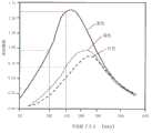
图4是根据本发明的基于LED的发光装置对于不同重量百分比装载的光反射材料的发射强度对色度CIE x的标绘图。4 is a plot of emission intensity versus chromaticity CIE x for LED-based lighting devices according to the present invention for different weight percent loadings of light reflective materials.
图5是根据本发明的替代实施例的基于LED的发光装置的示意图;5 is a schematic diagram of an LED-based lighting device according to an alternative embodiment of the present invention;
图6是根据本发明的另一实施例的基于LED的发光装置的示意图;6 is a schematic diagram of an LED-based lighting device according to another embodiment of the present invention;
图7是根据本发明的进一步实施例的基于LED的发光装置的示意图;7 is a schematic diagram of an LED-based lighting device according to a further embodiment of the present invention;
图8是说明图7的发光装置的操作原理的示意图;8 is a schematic diagram illustrating the operating principle of the light emitting device of FIG. 7;
图9是根据本发明的实施例的磷光体波长转换组件的示意图;Figure 9 is a schematic diagram of a phosphor wavelength conversion assembly according to an embodiment of the present invention;
图10是根据本发明的另一实施例的磷光体波长转换组件的示意图;10 is a schematic diagram of a phosphor wavelength conversion assembly according to another embodiment of the present invention;
图11展示红光、绿光及蓝光的相对光散射对于光衍射粒子尺寸(nm)的标绘图;Figure 11 shows a plot of relative light scattering versus light diffracting particle size (nm) for red, green, and blue light;
图12说明根据本发明的进一步实施例的基于LED的发光装置;以及Figure 12 illustrates an LED-based lighting device according to a further embodiment of the present invention; and
图13说明根据本发明的进一步实施例的图12的基于LED的发光装置的横截面图。13 illustrates a cross-sectional view of the LED-based lighting device of FIG. 12 according to a further embodiment of the invention.
具体实施方式Detailed ways
本发明的一些实施例是针对包括一个或一个以上固态发光体(通常为LED)的发光装置,所述一个或一个以上固态发光体可操作以产生激发光(通常为蓝色),其用于激发含有光致发光材料(例如,磷光体材料)(例如可激发蓝光的磷光体材料)粒子的波长转换组件。此外,所述波长转换组件包括与所述磷光体材料合并的光反射材料(在本文中还称为“光散射材料”)的粒子,以增强由所述磷光体材料产生的光致发光的光。增强的光产生源自所述光反射材料增加由所述发光体产生的光与所述磷光体材料的粒子碰撞的数目。最终结果是减少用于所述发光装置的磷光体材料使用。Some embodiments of the present invention are directed to lighting devices comprising one or more solid state light emitters (typically LEDs) operable to generate excitation light (typically blue) for use in A wavelength conversion component containing particles of a photoluminescent material (eg, phosphor material), such as a phosphor material that excites blue light, is excited. In addition, the wavelength conversion component includes particles of light reflective material (also referred to herein as "light scattering material") incorporated with the phosphor material to enhance photoluminescent light produced by the phosphor material. . Enhanced light production results from the light reflective material increasing the number of collisions of light generated by the light emitter with particles of the phosphor material. The end result is reduced phosphor material usage for the light emitting device.
仅出于说明目的,以下描述参考明确地体现为磷光体材料的光致发光材料而作出。然而,本发明可应用在任意类型的光致发光材料,例如磷光体材料或量子点。量子点是物质(例如,半导体)的一部分,其激发子被限制在所有三个空间维度中,所述激发子可由辐射能量激发,以发射特定波长或波长范围的光。因而,除非主张基于磷光体的波长转换组件,否则本发明并不限于基于磷光体的波长转换组件。此外,在此专利说明书中,相同参考数字用于指示相同部分。For purposes of illustration only, the following description is made with reference to photoluminescent materials that are expressly embodied as phosphor materials. However, the invention is applicable to any type of photoluminescent material, such as phosphor materials or quantum dots. A quantum dot is a portion of matter (eg, a semiconductor) whose excitons, which can be excited by radiant energy to emit light at a specific wavelength or range of wavelengths, are confined in all three spatial dimensions. Thus, the present invention is not limited to phosphor-based wavelength conversion components unless phosphor-based wavelength conversion components are claimed. Also, in this patent specification, the same reference numerals are used to designate the same parts.
图1展示根据本发明的实施例的基于LED的白色发光装置10的示意图。装置10包括蓝色发光LED12及位于所述LED远程的光致发光波长转换组件14。如所展示,波长转换组件14可包括光透射窗(衬底)16,其在至少一个面上具有磷光体转换层18。磷光体转换层18包括可激发蓝光的磷光体材料20的粒子、光反射材料22的粒子与光透射粘合剂材料24的混合物。光透射窗16可包括任意光透射材料,例如聚合物材料,例如,聚碳酸酯、丙烯酸、硅酮或环氧树脂或玻璃(例如石英玻璃)。通常,为了容易制造,光透射窗16是平面的,通常为圆盘形的形式,但其可取决于所要应用而为正方形、矩形或其它形状。在所述光透射窗是圆盘形时,直径可在约1cm与10cm之间,其是0.8cm2与80cm2之间的面积的光学孔径。在替代实施例中,预想光透射窗16包括以所选择的方向引导光的光学组件,例如凸透镜或凹透镜。为减少从LED12到波长转换组件14的热传递,尤其到所述磷光体材料的热传递,所述波长转换组件位于所述LED远程,物理上分离至少5mm的距离L。本发明的实施例涉及其中在所述LED远程提供所述波长转换组件及(更重要地)所述磷光体材料的装置,以减少从所述发光体到所述磷光体材料的热传递。在此申请案的上下文中,远程意指例如以空气间隙或光透射介质而在物理上分离。应了解,在远程磷光体装置中,所述磷光体材料分布在比所述LED的所述发光表面的面积(例如,0.03cm2)大很多的面积上(例如,0.8cm2到80cm2)。通常,所述磷光体材料分布在所述LED的发光面积的至少五十倍(通常至少100倍)的面积上。FIG. 1 shows a schematic diagram of an LED-based white
蓝色LED12可包括基于GaN(基于氮化镓)的LED,其可操作以产生具有在440nm到480nm的波长范围内(通常为465nm)的峰值波长λ1的蓝光26。蓝色LED12经配置以用蓝色激发光26照射波长转换组件14,由磷光体材料20吸收一定比例,且作为响应而发射不同波长λ2的光28,通常对于冷白色发光装置为黄-绿色。装置10的发射产物30(其经配置以呈现为白色)包括由LED发射的光26与由磷光体材料20产生的光28的组合。
磷光体材料20及光反射材料22(其为粉末形式)按已知比例与光透射粘合剂材料24彻底混合,光透射粘合剂材料24例如聚合物材料(例如,热可固化或UV可固化硅酮或环氧树脂材料),或透明墨水,例如UV可固化石版透明罩印PSLC-294。所述混合物作为具有均一厚度的一层或一个以上层而施覆到窗16的面。在优选实施例中,所述混合物通过网版印刷而施覆到所述光透射窗,且所述层的厚度t通过印刷次数而控制。如将对于所属领域的技术人员显而易见,所述磷光体/反射材料的混合物可使用其它方法施覆,包含喷墨印刷、旋涂,或使用刮刀(例如刮板)将所述混合物横扫于所述表面上(例如,刮刀涂敷)。The
在进一步实施例中,预想将磷光体与光反射材料的混合物在所述光透射窗中合并。例如,所述磷光体与光反射材料混合物可与光透射聚合物混合,且所述聚合物/磷光体混合物被挤出或射出成型,以形成具有遍及所述组件的体积而均匀地分布的所述磷光体及光反射材料的波长转换组件14。In a further embodiment, a mixture of phosphor and light reflective material is envisioned to be incorporated in said light transmissive window. For example, the phosphor and light reflective material mixture can be mixed with a light transmissive polymer, and the polymer/phosphor mixture extruded or injection molded to form all phosphors having a uniform distribution throughout the volume of the component. The
使所述磷光体材料位于所述LED远程提供许多优点,即减少所述磷光体材料的热降解。此外,对比于其中所述磷光体材料直接接触所述LED裸片的发光表面而提供的装置,远程地提供所述磷光体材料减少吸收由所述LED裸片背部散射的光。此外,使所述磷光体位在远程实现产生更一致色彩及/或CCT的光,因为对比于将所述磷光体直接提供在所述LED裸片的发光表面上,所述磷光体材料是提供在大得多的面积上。Locating the phosphor material remotely from the LED offers the advantage of reducing thermal degradation of the phosphor material. Furthermore, remotely providing the phosphor material reduces absorption of light backscattered by the LED die compared to devices where the phosphor material is provided in direct contact with the light emitting surface of the LED die. Furthermore, having the phosphor located remotely enables more consistent color and/or CCT light generation because the phosphor material is provided on over a much larger area.
所述磷光体材料可包括无机或有机磷光体,例如普通组合物A3Si(O,D)5或A2Si(O,D)4的基于硅酸盐的磷光体,其中Si是硅,O是氧,A包括锶(Sr)、钡(Ba)、镁(Mg)或钙(Ca),且D包括氯(Cl)、氟(F)、氮(N)或硫(S)。基于硅酸盐的磷光体的实例揭示于以下美国专利中:US7,575,697“铕激活的基于硅酸盐的绿色磷光体(Europium activatedsilicate-based green phosphor)”(让与给Intematix Corp.);US7,601,276“两相的基于硅酸盐的黄色磷光体(Two phase silicate-based yellow phosphor)”(让与给Intematix Corp.);US7,601,276“基于硅酸盐的橙色磷光体(Silicate-based orange phosphor)”(让与给IntematixCorp.)及US7,311,858“基于硅酸盐的黄绿色磷光体(Silicate-based yellow-greenphosphor)”(让与给Intematix Corp.)。所述磷光体还可包括基于铝酸盐的材料(例如我们同在申请中的第US2006/0158090号专利申请案“基于铝酸盐的绿色磷光体(Aluminate-based green phosphor)”及第US7,390,437号专利“基于铝酸盐的蓝色磷光体(Aluminate-based blue phosphor)”(让与给Intematix Corp.)中所教示)、硅酸铝磷光体(如在同在申请中的第US2008/0111472号申请案“硅酸铝橙红色磷光体(Aluminum-silicateorange-red phosphor)”中教示)或基于氮化物的红色磷光体材料(例如在2009年12月7日申请的同在申请中的第12/632,550号美国专利申请案中所教示)。应了解,所述磷光体材料并不限于本文中描述的实例,且可包括任意磷光体材料,包含氮化物及/或硫酸盐磷光体材料、氧氮化物及氧硫酸盐磷光体或石榴石材料(YAG)。The phosphor material may comprise inorganic or organic phosphors, such as silicate-based phosphors of the common compositionA3Si (O,D)5 orA2Si (O,D)4 , where Si is silicon, O is oxygen, A includes strontium (Sr), barium (Ba), magnesium (Mg) or calcium (Ca), and D includes chlorine (Cl), fluorine (F), nitrogen (N) or sulfur (S). Examples of silicate-based phosphors are disclosed in the following US patents: US7,575,697 "Europium activatedsilicate-based green phosphor" (assigned to Intematix Corp.); US7 , 601,276 "Two phase silicate-based yellow phosphor (Two phase silicate-based yellow phosphor)" (ceded to Intematix Corp.); US7,601,276 "Silicate-based orange phosphor (Silicate-based orange phosphor)"phosphor)" (assigned to Intematix Corp.) and US7,311,858 "Silicate-based yellow-green phosphor (assigned to Intematix Corp.)". The phosphors may also include aluminate-based materials (such as our co-pending patent application US2006/0158090 "Aluminate-based green phosphor" and US7, 390,437 "Aluminate-based blue phosphor" (assigned to Intematix Corp. ), aluminum silicate phosphors (as taught in co-pending US2008/ 0111472 application "Aluminum-silicate orange-red phosphor (Aluminum-silicate orange-red phosphor)" or a nitride-based red phosphor material (such as in the co-pending application No. 12/632,550, as taught in US Patent Application No. 12/632,550). It should be appreciated that the phosphor materials are not limited to the examples described herein, and may include any phosphor material, including nitride and/or sulfate phosphor materials, oxynitride and oxysulfate phosphors, or garnet materials (YAG).
所述磷光体材料包括大体上为具有10μm到20μm且通常为15μm数量级的直径的球形形式的粒子。所述磷光体材料可包括2μm到60μm的尺寸的粒子。The phosphor material comprises particles in substantially spherical form having a diameter of the order of 10 μm to 20 μm and typically of the order of 15 μm. The phosphor material may comprise particles with a size of 2 μm to 60 μm.
光反射材料22包括具有较高反射率(通常为0.9或更高的反射系数)的粉末材料。所述光反射材料的粒子尺寸通常在0.1μm到10μm的范围内,且在优选实施例中在0.1μm到10μm的范围内。光反射材料对磷光体材料的重量百分比装载在0.1%到10%的范围内,且在优选实施例中在1%到2%的范围内。光反射材料的实例包含氧化镁(MgO)、二氧化钛(TiO2)、硫酸钡(BaSO4),及其组合。所述光反射材料还可包括白色墨水,例如Norcote International Inc.的超级白色墨水GN-027SA,其已包含高度光反射材料(通常为TiO2)的粒子。The light
在描述本发明的装置的操作之前,将参考图2描述已知发光装置的操作,图2展示利用磷光体波长转换的基于冷白色LED的发光装置的示意图。与本发明的装置一样,所述已知装置包含波长转换组件18,其包含遍及光透射粘合剂24的体积而均匀分布的磷光体材料粒子20。不像本发明的装置,所述已知装置并不包含光反射材料的粒子。在操作中,来自所述LED的蓝光26由光透射粘合剂24传输,直到其撞击磷光体材料的粒子。相信光子与磷光体材料粒子的交互作用平均只有万分之一导致光致发光的光的吸收及产生。光子与磷光体粒子的交互作用的大部分(约99.99%)导致所述光子的散射。由于散射过程的各向同性本质,平均一半的散射光子将在往回朝向所述LED的方向中。测试指示通常全部入射蓝光的约10%在往回朝向所述LED的方向中从所述波长转换组件散射且发射。对于冷白色发光装置,磷光体材料的量经选择以允许全部入射蓝光的约10%被发射穿过所述窗,且促成发射产物的形成。所述入射光的大部分(约80%)被所述磷光体材料吸收,且重新发射为光致发光的光28。由于光致发光的光产生的各向同性本质,由所述磷光体材料产生的约一半的光28将在朝向所述LED的方向中发射。结果,全部入射光的至多(↑)40%将发射为波长λ2的光28,且促成发射产物30的形成,而全部入射光的至多(↑)40%将在往回朝向所述LED的方向中发射为波长λ2的光28。通常,朝向所述LED发射的光由反射镜(未展示)重新引导,以增加所述装置的总体效率。Before describing the operation of the device of the present invention, the operation of a known lighting device will be described with reference to Figure 2, which shows a schematic diagram of a cool white LED based lighting device utilizing phosphor wavelength conversion. As with the device of the present invention, the known device comprises a
现参考图3描述根据本发明的一些实施例的冷白色发光装置10的操作,图3展示图1的装置的操作的示意图。本发明的装置的操作类似于图2,但额外地包含由所述光反射/散射材料的粒子的反射或散射光(波长为λ1及λ2)。通过包含光反射材料与所述磷光体材料的粒子,此可减少产生给定色彩的发射产物所需的磷光体材料的量,例如,在一些实施例中减少多达33%。相信光反射材料的粒子增加光子撞击磷光体材料的粒子的可能性,且因此对于给定色彩的发射产物,需要较少磷光体材料。The operation of the cool white
图4是根据本发明的一些实施例的发光装置对于◆-0%、■-0.4%、▲-1.1%及●-2%的光反射材料的重量百分比装载的发射强度对色度CIE x的标绘图。数据是针对网版印刷磷光体转换层,其中粘合剂材料包括
图5是根据本发明的另一实施例的基于LED的白色发光装置10的示意图。在此实施例中,光透射衬底16配置为光导(波导),且磷光体转换层18提供在所述衬底的一个面(发光面)上。通常,衬底16是实质上平面的,且取决于应用可为圆盘形、正方形、矩形或其它形状。在所述衬底是圆盘形时,所述直径可通常在约5cm与30cm之间,对应于约20cm2与约700cm2之间的面积的发光面。在所述衬底形式为正方形或矩形时,各边可通常在约5cm与40cm之间,对应于约80cm2与约5000cm2之间的发光面。在所述衬底16的非发光面(如所说明的下方表面)上,可提供一层光反射材料44以防止来自所述装置后方的光发射。反射材料44可包括金属涂层,例如铬,或有光泽的白色材料,例如塑料材料或纸。为使从所述衬底边缘发射的光最小化,所述衬底的边缘优选地包含光反射表面(未展示)。一个或一个以上蓝色LED12经配置以将蓝光26耦合到衬底16的一个或一个以上边缘。在操作中,耦合到衬底16的光26通过全内反射而被引导遍及衬底16的整个体积。以大于临界角的角度撞击所述衬底的发光面的光26将被发射通过所述发光面,且进入磷光体波长转换层18。所述装置的操作与参考图3描述的操作相同。如图5中所指示,以离开所述发光面的方向发射的磷光体产生的光46可重新进入衬底16,且最终由于光反射层44的反射而发射通过发光面。从所述装置发射的最终照明产物30是由所述LED产生的蓝光26与由所述磷光体波长转换层18产生的波长转换的光28的组合。FIG. 5 is a schematic diagram of an LED-based white
图6是替代的基于LED的白色发光装置10的示意图,其中光透射衬底16配置为光导(波导)。在此实施例中,磷光体转换层18提供在所述衬底的与发光面相对的面上,且光反射层44提供在所述磷光体转换层18上。Figure 6 is a schematic diagram of an alternative LED-based white
图7展示根据本发明的进一步实施例的基于LED的白色发光装置10的示意图。在此实施例中,波长转换组件14是光反射的,且包括光反射表面48,其上施覆磷光体转换层18。如所展示,光反射表面48可包括抛物面表面,但其还可包括任意表面,包含平面、凸面及凹面。为使从所述装置的光发射最大化,所述光反射表面尽可能具反射性,且优选地具有至少0.9的反射系数。所述光反射表面可包括:抛光金属表面,例如银、铝、铬;光反射聚合物;光反射纸或光反射涂料。为帮助热消散,所述光反射表面优选为导热的。Fig. 7 shows a schematic diagram of an LED-based white
图7的发光装置的操作在图8中说明,且因其类似于图3的操作,故不详细描述。然而,应了解,因为平均多达一半的LED光26将传播通过所述磷光体转换层两次,故所述磷光体转换层18的厚度可对比于具有光透射波长转换组件的布置(图1及图5)而为至多一半,即,t/2。由于将所述磷光体材料提供在光反射表面上,故可在磷光体材料使用上以多达约50%的进一步潜在缩减实现相同色彩的发射产物。应了解,图6的实施例在操作上与图7的操作类似,光透射衬底16用于将LED光26引导到磷光体转换层18。The operation of the lighting device of FIG. 7 is illustrated in FIG. 8 and will not be described in detail because it is similar to the operation of FIG. 3 . However, it should be appreciated that the thickness of the
虽然本发明已关于发光装置加以描述,但本发明的原理还适用于利用光致发光波长转换以产生期望色彩的发射光的固态发光标牌,例如Li等人的同在申请中的US2007/0240346A1美国专利申请案中所揭示,其说明书以引用的方式并入本文中。应了解,在此些发光标志中,波长转换组件14可用作所述光致发光标牌表面,以产生期望色彩的标牌信息。磷光体材料与光反射材料的混合物可配置为图案,以在所述光透射衬底上定义图像、图片、字母、数字、装置、图案或其它标牌信息。或者,例如为刻槽型文字所需要的,所述标牌表面的形状(即,所述光透射衬底)可经配置以定义标牌信息。本发明在标牌表面的面积为几百平方厘米的标牌应用中尤其有利,此要求所述磷光体材料分布在100cm2的最小面积上(10cm×10cm),且更通常超过几百平方厘米或甚至几千平方厘米。While the invention has been described in relation to light emitting devices, the principles of the invention are also applicable to solid state light emitting signs utilizing photoluminescence wavelength conversion to produce emitted light of a desired color, such as co-pending application US2007/0240346A1 to Li et al. Disclosed in the patent application, the specification of which is incorporated herein by reference. It will be appreciated that in such illuminated signs, the
所述标志可为背光,即,所述LED位于例如灯箱内的标牌表面后,且所述标牌表面覆盖所述灯箱开口而提供。通常,所述标牌表面位于距所述LED至少约5mm的距离处。或者,所述标志可为边缘照亮的,且所述光透射衬底配置为光导,且磷光体材料与光反射材料的混合物提供在所述光导的发光面的至少一部分上。The signage may be backlit, ie the LEDs are provided behind a signage surface, for example within a light box, and the signage surface covers the light box opening. Typically, the signage surface is located at a distance of at least about 5 mm from the LEDs. Alternatively, the logo may be edge lit and the light transmissive substrate configured as a light guide and a mixture of phosphor material and light reflective material is provided on at least a portion of the light emitting face of the light guide.
在一些实施例中,所述光反射材料包括二氧化钛(TiO2),但其也可包括其它材料,例如硫酸钡(BaSO4)、氧化镁(MgO)、二氧化硅(SiO2)或氧化铝(Al2O3)。在一些实施例中,所述光反射材料具有在1μm到50μm的范围内的平均粒子尺寸,且更优选地在10μm到20μm的范围内。In some embodiments, the light reflective material comprises titanium dioxide (TiO2 ), but it may also comprise other materials such as barium sulfate (BaSO4 ), magnesium oxide (MgO), silicon dioxide (SiO2 ) or aluminum oxide (Al2 O3 ). In some embodiments, the light reflective material has an average particle size in the range of 1 μm to 50 μm, and more preferably in the range of 10 μm to 20 μm.
在一些实施例中,用于所述波长转换组件中的光反射/散射材料具有粒子尺寸,所述粒子尺寸经选择使得比起所述粒子将散射由所述光致发光(磷光体)材料产生的光,其将散射相对更多激发(通常为蓝色)光。例如,所述光反射粒子尺寸可经选择使得比起所述粒子将散射由所述至少一种磷光体材料产生的光,其将散射相对至少两倍的激发光。此确保将散射更高比例的蓝色激发光,增加光子与磷光体材料粒子交互作用的可能性,且导致产生光致发光的光。同时,磷光体产生的光可以被散射的较低可能性通过。In some embodiments, the light reflecting/scattering material used in the wavelength conversion component has a particle size selected such that the particles will scatter more light than would be produced by the photoluminescent (phosphor) material. , which will scatter relatively more excitation (usually blue) light. For example, the light reflective particle size may be selected such that it will scatter at least twice as much excitation light as the particle will scatter light generated by the at least one phosphor material. This ensures that a higher proportion of the blue excitation light will be scattered, increasing the likelihood of photons interacting with the phosphor material particles and resulting in photoluminescent light. At the same time, the light generated by the phosphor can pass through with a lower probability of being scattered.
因为此方法可进一步增加蓝色光子与磷光体材料粒子交互作用的可能性,因此需要较少磷光体材料以产生选择发射色彩。此布置还可增加所述波长转换组件/装置的发光效率。在利用蓝色(400nm到480nm)激发光的一些实施例中,所述光反射材料具有小于约150nm的平均粒子尺寸,且通常具有在100nm到150nm的范围内的平均粒子尺寸。Because this approach can further increase the probability of blue photons interacting with the phosphor material particles, less phosphor material is required to produce the selective emission color. This arrangement may also increase the luminous efficiency of the wavelength conversion component/device. In some embodiments utilizing blue (400nm to 480nm) excitation light, the light reflective material has an average particle size of less than about 150nm, and typically has an average particle size in the range of 100nm to 150nm.
所述光反射/散射材料(即,用于优先散射蓝光)可在与所述磷光体材料相同的材料层中体现。The light reflecting/scattering material (ie for preferentially scattering blue light) may be embodied in the same material layer as the phosphor material.
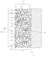
或者,所述光反射/散射材料可置于邻近于或接近具有所述磷光体材料的层的分离层上。例如,根据本发明的一些实施例且如图9中所展示,波长转换组件136按顺序包括光透射衬底142;光反射层144,其含有光反射粒子;及波长转换层146,其含有一种或一种以上磷光体(光致发光)与光反射材料的混合物。如图9中可见,波长转换组件136经配置使得在操作中,波长转换层146面对所述LED。根据本发明的一些实施例,波长转换组件136可按顺序包括光透射衬底142;光反射层144,其含有光反射粒子;及波长转换层146,其含有一种或一种以上磷光体(光致发光)材料。Alternatively, the light reflecting/scattering material may be placed on a separate layer adjacent to or close to the layer with the phosphor material. For example, according to some embodiments of the invention and as shown in FIG. 9 , the
光透射衬底142可为对380nm到740nm的波长范围内的光实质上透射的任意材料,且可包括光透射聚合物(例如聚碳酸酯或丙烯酸)或玻璃(例如硼硅酸盐玻璃)。在一些实施例中,衬底142包括直径为
光扩散层144包括光反射材料(优选地为二氧化钛(TiO2))的粒子的均匀厚度层。在替代配置中,所述光反射材料可包括硫酸钡(BaSO4)、氧化镁(MgO)、二氧化硅(SiO2)、氧化铝(Al2O3)或具有尽可能高的反射率(通常为0.9或更高的反射系数)的粉末材料。所述光反射材料粉末以已知比例与光透射液体粘合剂材料彻底混合,以形成悬浮液,且所得的混合物优选地通过网版印刷而沉积在衬底142的面上,以形成遮盖所述衬底的整个面的厚度t2(通常在10μm到75μm的范围内)的均匀层。在光扩散层144中,每单位面积的光衍射材料的量将通常在10μg.cm-2到5mg.cm-2的范围内。
虽然网版印刷是沉积光扩散层144的优选方法,但其还可使用其它技术沉积,例如槽模式涂布(slot die coating)、旋涂、滚涂、下拉式涂布(drawdown coating)或刮刀涂敷。所述粘合剂材料可包括可固化液体聚合物,例如聚合物树脂、单体树脂、丙烯酸、环氧树脂(聚环氧化物)、硅酮或氟化聚合物。所述粘合剂材料在其固化状态中对由所述磷光体材料及所述LED产生的所有波长的光实质上透射是重要的,且优选地对于可见光谱(380nm到800nm)具有至少0.9的透射系数。所述粘合剂材料优选地为UV可固化的,但其也可为可热固化的、基于溶剂的或其组合。可UV固化或热固化的粘合剂可为优选的,因为不像基于溶剂的材料,其并不在聚合作用期间“释气(outgas)”。在一种布置中,所述光衍射材料的平均粒子尺寸在5μm到15μm的范围内,但如上文所描述,其还可在纳米范围(nm)内,且宜在100nm到150nm的范围内。光反射材料对液体粘合剂的重量百分比装载通常在7%到35%的范围内。While screen printing is the preferred method of depositing the
波长转换层146与光扩散层144直接接触而沉积,即没有任何中介层或空气间隙。所述磷光体材料(其是粉末形式)以已知比例与液体光透射粘合剂材料彻底混合,以形成悬浮液,且所得的磷光体组合物(“磷光体墨水”)直接沉积在反射层144上。所述波长转换层优选地通过网版印刷而沉积,但也可使用其它沉积技术,例如槽模式涂布、旋涂或刮刀涂敷。为消除波长转换层146与反射层144之间的光学接口,且使这两层之间的光透射最大化,优选地使用相同液体粘合剂材料制造两个层;即,聚合物树脂、单体树脂、丙烯酸、环氧树脂、硅酮或氟化聚合物。The
根据本发明的磷光体波长转换组件136的进一步实例在图10中说明。与图9的波长转换组件一样,所述组件包括光透射衬底142、光扩散层144及波长转换层146。根据本发明,光扩散层144及波长转换层146彼此直接接触而沉积。同样地,在操作中,所述组件经配置使得所述波长转换组件经配置使得波长转换层146面对所述LED。A further example of a phosphor
在操作中,由所述LED产生的蓝色激发光128传播通过波长转换层146,直到其撞击磷光体材料的粒子。相信光子与磷光体材料粒子的交互作用平均只有万分之一导致光致发光的光138的吸收及产生。光子与磷光体粒子的交互作用的大部分(约99.99%)导致所述光子的散射。由于散射过程的各向同性本质,平均一半的光子将在往回朝向所述LED的方向中散射。测试指示通常全部入射蓝光128的约10%在往回朝向所述LED的方向中从波长转换组件136散射且发射。对于冷白色发光装置,磷光体材料的量经选择以允许全部入射蓝光的约10%从所述波长转换组件发射,且促成发射产物140的形成。所述入射光的大部分(约80%)被所述磷光体材料吸收,且重新发射为光致发光的光138。由于光致发光产生的各向同性本质,由所述磷光体材料产生的约一半的光138将在朝向所述LED的方向中被发射。结果,全部入射光的仅至多约40%将发射为波长λ2的光138,且促成发射产物138的形成,其中全部入射光的剩余部分(至多约40%)将在往回朝向所述LED的一方向中发射为波长λ2的光138。从波长转换组件136朝向所述LED发射的光由反射腔室的光反射表面重新引导,以促成所述发射产物的形成,且增加所述装置的总体效率。In operation, the
添加由光反射材料的粒子组成的光扩散层144可实质上减少产生所选择色彩的发射光所需的磷光体材料的量。扩散层144通过将光反射回波长转换层146中而增加光子将导致产生光致发光的光的可能性。包含与所述波长转换层直接接触的反射层可减少产生给定色彩的发射产物所需的磷光体材料的量,例如在一些实施例中减少多达40%。The addition of a
因此,预想配置所述光扩散层,使得比起其散射由所述磷光体材料产生的光,其选择性地散射更多由所述LED产生的蓝色激发光。此光扩散层确保从所述波长转换层发射的更高比例的蓝光将被散射,且由所述光反射材料引导回所述波长转换层中,增加所述光子与磷光体材料粒子交互作用的可能性,且导致产生光致发光的光。同时,磷光体产生的光可以被散射的较低可能性通过所述扩散层。因为所述扩散层增加蓝色光子与磷光体材料粒子交互作用的可能性,因此产生所选择的发射色彩需要较少磷光体材料。Accordingly, it is envisioned to configure the light diffusing layer so that it selectively scatters more of the blue excitation light produced by the LED than it scatters light produced by the phosphor material. This light diffusing layer ensures that a higher proportion of the blue light emitted from the wavelength converting layer will be scattered and directed back into the wavelength converting layer by the light reflective material, increasing the chances of the photons interacting with phosphor material particles possibility, and lead to the generation of photoluminescent light. At the same time, the light generated by the phosphor can pass through the diffusion layer with a lower probability of being scattered. Because the diffusing layer increases the probability of blue photons interacting with the phosphor material particles, less phosphor material is required to produce the selected emission color.
此外,此配置还可增加所述波长转换组件/装置的发光效率。通过适当选择所述光散射材料的平均粒子尺寸,可配置所述光扩散层使得其散射蓝光比散射其它色彩(即绿色及红色)更容易。图11展示红光、绿光及蓝光的相对光散射对照TiO2平均粒子尺寸(nm)的标绘图。如从图11可见,具有100nm到150nm的平均粒子尺寸的TiO2粒子比起其将散射绿光(510nm到550nm)或红光(630nm到740nm),散射蓝光(450nm到480nm)可能超过两倍。例如,具有100nm的平均粒子尺寸的TiO2粒子比起其将散射绿光或红光,将以近三倍(2.9=0.97/0.33)散射更多蓝光。对于具有200nm的平均粒子尺寸的TiO2粒子,比起其将散射绿光或红光,其将散射超过两倍(2.3=1.6/0.7)的蓝光。根据本发明的一些实施例,所述光衍射粒子尺寸优选地经选择使得所述粒子将散射比由所述磷光体材料产生的光相对多至少两倍的蓝光。包含由光反射粒子(与由所述磷光体材料产生的波长的光相比,其优先散射对应于由所述LED产生的波长的光)组成的光反射层的波长转换组件的概念客观地被视为是发明性的。In addition, this configuration can also increase the luminous efficiency of the wavelength conversion component/device. By properly selecting the average particle size of the light scattering material, the light diffusing layer can be configured so that it scatters blue light more readily than other colors (ie green and red). Figure 11 shows a plot of relative light scattering for red, green, and blue light versusTi02 mean particle size (nm). As can be seen from Figure 11,TiO2 particles having an average particle size of 100nm to 150nm are more than twice as likely to scatter blue light (450nm to 480nm) than they would be to scatter green light (510nm to 550nm) or red light (630nm to 740nm) . For example,Ti02 particles with an average particle size of 100 nm will scatter blue light nearly three times (2.9=0.97/0.33) more than they will scatter green or red light. For aTi02 particle with an average particle size of 200 nm, it will scatter more than twice (2.3=1.6/0.7) blue light than it will scatter green or red light. According to some embodiments of the invention, the light diffractive particle size is preferably selected such that the particles will scatter at least two times relatively more blue light than the light produced by the phosphor material. The concept of a wavelength conversion component comprising a light-reflecting layer composed of light-reflecting particles that preferentially scatter light corresponding to the wavelength generated by the LED compared to the wavelength generated by the phosphor material is objectively recognized. considered to be inventive.
因此,所述光反射/散射材料可以邻近于或接近包含所述磷光体材料的一层的分离层体现。所述分离光反射层可用于替代将光反射/散射材料混合到与所述磷光体材料相同的层中,及/或除了将光反射/散射材料混合到与所述磷光体材料相同的层中之外而使用。分离的光反射层中可使用与所述磷光体材料混合的所述光反射材料相同或不同的反射材料。Thus, the light reflecting/scattering material may be embodied adjacent to or close to a separate layer comprising a layer of the phosphor material. The separate light reflective layer can be used instead of, and/or in addition to, mixing a light reflective/scattering material into the same layer as the phosphor material use outside. The same or different reflective material as the light reflective material mixed with the phosphor material may be used in a separate light reflective layer.
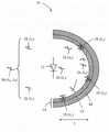
本文中揭示的发明性概念可应用在涵盖任意适宜形状的波长转换组件。例如,考虑在图12及图13中说明的LED照明装置200,其展示代替白炽灯泡的固态灯泡。The inventive concepts disclosed herein are applicable to wavelength conversion components encompassing any suitable shape. For example, consider the
LED照明装置200包括照明基座204,其包含螺纹基座206。螺纹基座206经配置以安装在标准灯泡插座中,例如实施为标准爱迪生螺纹基座(Edison screw base)。外包体208可绕LED照明装置200的上方部分延伸。外包体208是光透射材料(例如,玻璃或塑料),其对LED照明装置200提供保护及/或扩散性质。The
LED照明装置200包括波长转换组件202,波长转换组件202具有从照明基座204延伸的伸长圆顶形。蓝色LED装置12位于照明基座204的顶面上,在波长转换组件202之下。波长转换组件202的三维本质建立围绕体积四周且在LED12上方的相对较大形状。在照明装置200中对波长转换组件202使用三维形状允许某些功能性优点,例如对由照明装置200发射的光执行光塑形。
然而,波长转换组件202的此些类型的三维形状也对应于相对较大体积的波长转换组件,其需要用足够量的磷光体材料装填。在现有技术方法的情况下,因此将需要明显较大量的磷光体材料,以制造此些波长转换组件202。可利用本发明的实施例以减少制造此些波长转换组件202所需的磷光体的量。特定来说,波长转换组件202包括磷光体与反射材料的混合物。因为波长转换组件202内的反射性材料具有散射光的性质,此减少用于波长转换组件202所需的磷光体的量。However, these types of three-dimensional shapes of the
在一些实施例中,可将光扩散层(未作图式)添加到波长转换组件202(除了与所述磷光体混合的反射材料外,及/或替代与所述磷光体混合的反射材料),以减少制造波长转换组件202所需的磷光体材料的量。所述光反射材料可利用任意适宜材料,例如经选择为足够小的光散射粒子,以更可能散射蓝光。In some embodiments, a light diffusing layer (not shown) may be added to the wavelength conversion component 202 (in addition to, and/or instead of, the reflective material mixed with the phosphor) , to reduce the amount of phosphor material required to manufacture the
因此,已描述用于实施基于LED的照明装置及/或减少制造此些装置及组件所需的光致发光材料的量的波长转换组件的改进方法。Accordingly, improved methods for implementing LED-based lighting devices and/or wavelength converting components that reduce the amount of photoluminescent material required to fabricate such devices and components have been described.
应了解,根据本发明的发光装置并不限于所描述的示范性实施例,且在本发明的范围内可作出变动。例如,虽然本发明已关于基于LED的发光装置加以描述,但本发明还适用于基于其它固态发光体(包含固态激光及激光二极管)的装置。It will be appreciated that the lighting device according to the invention is not limited to the described exemplary embodiments and that variations may be made within the scope of the invention. For example, while the invention has been described with respect to LED-based light emitting devices, the invention is also applicable to devices based on other solid state light emitters, including solid state lasers and laser diodes.
Claims (24)
Applications Claiming Priority (5)
| Application Number | Priority Date | Filing Date | Title |
|---|---|---|---|
| US39009110P | 2010-10-05 | 2010-10-05 | |
| US61/390,091 | 2010-10-05 | ||
| US201061427411P | 2010-12-27 | 2010-12-27 | |
| US61/427,411 | 2010-12-27 | ||
| PCT/US2011/054827WO2012047937A1 (en) | 2010-10-05 | 2011-10-04 | Solid-state light emitting devices and signage with photoluminescence wavelength conversion |
Publications (2)
| Publication Number | Publication Date |
|---|---|
| CN103155024Atrue CN103155024A (en) | 2013-06-12 |
| CN103155024B CN103155024B (en) | 2016-09-14 |
Family
ID=45924446
Family Applications (1)
| Application Number | Title | Priority Date | Filing Date |
|---|---|---|---|
| CN201180048303.5AActiveCN103155024B (en) | 2010-10-05 | 2011-10-04 | Solid state light emitting device and signage with photoluminescence wavelength conversion |
Country Status (6)
| Country | Link |
|---|---|
| US (2) | US8610340B2 (en) |
| JP (1) | JP6069205B2 (en) |
| KR (1) | KR20130139938A (en) |
| CN (1) | CN103155024B (en) |
| TW (2) | TWI504968B (en) |
| WO (1) | WO2012047937A1 (en) |
Cited By (6)
| Publication number | Priority date | Publication date | Assignee | Title |
|---|---|---|---|---|
| CN105679918A (en)* | 2016-04-06 | 2016-06-15 | 苏州星烁纳米科技有限公司 | Wavelength conversion device and preparation method and application thereof |
| CN106195925A (en)* | 2015-04-29 | 2016-12-07 | 深圳市光峰光电技术有限公司 | A kind of Wavelength converter, light-emitting device and projection arrangement |
| CN110676358A (en)* | 2019-11-04 | 2020-01-10 | 佛山市国星半导体技术有限公司 | High-brightness normally-installed LED chip and manufacturing method thereof |
| CN110691941A (en)* | 2017-03-28 | 2020-01-14 | 康宁公司 | Light Diffusion Fibers for White Light Emitting |
| CN111679493A (en)* | 2020-05-29 | 2020-09-18 | 太湖金张科技股份有限公司 | Backlight module with blue light conversion reflection film and liquid crystal display panel |
| CN116210082A (en)* | 2019-10-25 | 2023-06-02 | 亮锐有限责任公司 | Coloring and scattering particles in side coating materials for LED applications |
Families Citing this family (37)
| Publication number | Priority date | Publication date | Assignee | Title |
|---|---|---|---|---|
| US20080029720A1 (en)* | 2006-08-03 | 2008-02-07 | Intematix Corporation | LED lighting arrangement including light emitting phosphor |
| US11114594B2 (en) | 2007-08-24 | 2021-09-07 | Creeled, Inc. | Light emitting device packages using light scattering particles of different size |
| US9287469B2 (en) | 2008-05-02 | 2016-03-15 | Cree, Inc. | Encapsulation for phosphor-converted white light emitting diode |
| CA2760767C (en)* | 2009-05-04 | 2018-01-30 | Koninklijke Philips Electronics N.V. | Light source comprising a light emitter arranged inside a translucent outer envelope |
| US8415692B2 (en) | 2009-07-06 | 2013-04-09 | Cree, Inc. | LED packages with scattering particle regions |
| US9546765B2 (en) | 2010-10-05 | 2017-01-17 | Intematix Corporation | Diffuser component having scattering particles |
| US8610341B2 (en) | 2010-10-05 | 2013-12-17 | Intematix Corporation | Wavelength conversion component |
| US8604678B2 (en) | 2010-10-05 | 2013-12-10 | Intematix Corporation | Wavelength conversion component with a diffusing layer |
| US8957585B2 (en) | 2010-10-05 | 2015-02-17 | Intermatix Corporation | Solid-state light emitting devices with photoluminescence wavelength conversion |
| CN103155024B (en) | 2010-10-05 | 2016-09-14 | 英特曼帝克司公司 | Solid state light emitting device and signage with photoluminescence wavelength conversion |
| US8614539B2 (en) | 2010-10-05 | 2013-12-24 | Intematix Corporation | Wavelength conversion component with scattering particles |
| JP5770205B2 (en)* | 2010-11-22 | 2015-08-26 | 宇部マテリアルズ株式会社 | Silicate phosphor and light emitting device exhibiting high light emission characteristics and moisture resistance |
| DE102011014845B4 (en)* | 2011-03-23 | 2023-05-17 | OSRAM Opto Semiconductors Gesellschaft mit beschränkter Haftung | Semiconductor light-emitting device and method of manufacturing a semiconductor light-emitting device |
| US9897276B2 (en)* | 2011-08-26 | 2018-02-20 | Cree, Inc. | Reduced phosphor lighting devices |
| WO2013115379A1 (en)* | 2012-02-02 | 2013-08-08 | シチズンホールディングス株式会社 | Semiconductor light emitting device and fabrication method for same |
| ITTO20120988A1 (en)* | 2012-11-14 | 2014-05-15 | Light In Light S R L | ARTIFICIAL LIGHTING SYSTEM TO SIMULATE A NATURAL LIGHTING |
| US20140185269A1 (en)* | 2012-12-28 | 2014-07-03 | Intermatix Corporation | Solid-state lamps utilizing photoluminescence wavelength conversion components |
| US9217543B2 (en) | 2013-01-28 | 2015-12-22 | Intematix Corporation | Solid-state lamps with omnidirectional emission patterns |
| US9057488B2 (en)* | 2013-02-15 | 2015-06-16 | Wavien, Inc. | Liquid-cooled LED lamp |
| CN105074320B (en)* | 2013-03-11 | 2019-05-14 | 飞利浦照明控股有限公司 | Light-emitting diode (LED) module with improved light characteristic |
| WO2014151263A1 (en) | 2013-03-15 | 2014-09-25 | Intematix Corporation | Photoluminescence wavelength conversion components |
| EP2851612B1 (en)* | 2013-09-24 | 2019-06-26 | Glashütte Limburg Leuchten GmbH + Co. KG | Lamp with lampshade |
| US20150085466A1 (en)* | 2013-09-24 | 2015-03-26 | Intematix Corporation | Low profile led-based lighting arrangements |
| JP2015144261A (en)* | 2013-12-26 | 2015-08-06 | インテマティックス・コーポレーションIntematix Corporation | Solid-state light emitting device with photoluminescence wavelength conversion |
| JP6503710B2 (en)* | 2013-12-27 | 2019-04-24 | 日本電気硝子株式会社 | Fluorescent wheel for projector, method of manufacturing the same, and light emitting device for projector |
| JP6622187B2 (en) | 2014-04-08 | 2019-12-18 | Nsマテリアルズ株式会社 | Wavelength conversion member, light guide device, and display device |
| US9706084B2 (en) | 2014-07-30 | 2017-07-11 | Hewlett-Packard Development Company, L.P. | Color mapping |
| KR20160016413A (en) | 2014-08-05 | 2016-02-15 | 삼성전자주식회사 | Display system and control method of the same |
| TWI612694B (en)* | 2014-11-18 | 2018-01-21 | 錼創科技股份有限公司 | Light-emitting element manufacturing method |
| KR20170101942A (en)* | 2015-01-06 | 2017-09-06 | 코닝 인코포레이티드 | Electrodeless organic light-emitting device and lcd systems using same |
| WO2016133825A1 (en)* | 2015-02-19 | 2016-08-25 | Osram Sylvania Inc. | Led light source with diffuser |
| US10066160B2 (en) | 2015-05-01 | 2018-09-04 | Intematix Corporation | Solid-state white light generating lighting arrangements including photoluminescence wavelength conversion components |
| AU2016100318B4 (en)* | 2015-05-11 | 2016-08-04 | X Tec Pty Ltd | A low energy building |
| JP7014718B2 (en)* | 2015-12-23 | 2022-02-01 | アファンタマ アクチェンゲゼルシャフト | Display device |
| TWI579635B (en)* | 2015-12-28 | 2017-04-21 | 中強光電股份有限公司 | Projection system and screen thereof |
| US10753577B2 (en)* | 2016-01-19 | 2020-08-25 | Signify Holdings B.V. | Lighting device |
| DE102019108995A1 (en)* | 2019-04-05 | 2020-10-08 | HELLA GmbH & Co. KGaA | Lighting device for vehicles |
Citations (3)
| Publication number | Priority date | Publication date | Assignee | Title |
|---|---|---|---|---|
| CN101375420A (en)* | 2006-01-24 | 2009-02-25 | 皇家飞利浦电子股份有限公司 | Light-emitting device |
| CN101421855A (en)* | 2006-03-08 | 2009-04-29 | 英特曼帝克司公司 | Luminous sign and display surface thereof |
| US20090272996A1 (en)* | 2008-05-02 | 2009-11-05 | Cree, Inc. | Encapsulation for phosphor-converted white light emitting diode |
Family Cites Families (165)
| Publication number | Priority date | Publication date | Assignee | Title |
|---|---|---|---|---|
| US3290255A (en) | 1963-09-30 | 1966-12-06 | Gen Electric | White electroluminescent phosphor |
| US3593055A (en) | 1969-04-16 | 1971-07-13 | Bell Telephone Labor Inc | Electro-luminescent device |
| US3676668A (en) | 1969-12-29 | 1972-07-11 | Gen Electric | Solid state lamp assembly |
| US3691482A (en) | 1970-01-19 | 1972-09-12 | Bell Telephone Labor Inc | Display system |
| GB1311361A (en) | 1970-02-19 | 1973-03-28 | Ilford Ltd | Electrophotographic material |
| US4104076A (en) | 1970-03-17 | 1978-08-01 | Saint-Gobain Industries | Manufacture of novel grey and bronze glasses |
| US3670193A (en) | 1970-05-14 | 1972-06-13 | Duro Test Corp | Electric lamps producing energy in the visible and ultra-violet ranges |
| NL7017716A (en) | 1970-12-04 | 1972-06-06 | ||
| JPS5026433B1 (en) | 1970-12-21 | 1975-09-01 | ||
| BE786323A (en) | 1971-07-16 | 1973-01-15 | Eastman Kodak Co | REINFORCING SCREEN AND RADIOGRAPHIC PRODUCT THE |
| JPS48102585A (en) | 1972-04-04 | 1973-12-22 | ||
| US3932881A (en) | 1972-09-05 | 1976-01-13 | Nippon Electric Co., Inc. | Electroluminescent device including dichroic and infrared reflecting components |
| US4081764A (en) | 1972-10-12 | 1978-03-28 | Minnesota Mining And Manufacturing Company | Zinc oxide light emitting diode |
| US3819973A (en) | 1972-11-02 | 1974-06-25 | A Hosford | Electroluminescent filament |
| US3849707A (en) | 1973-03-07 | 1974-11-19 | Ibm | PLANAR GaN ELECTROLUMINESCENT DEVICE |
| US3819974A (en) | 1973-03-12 | 1974-06-25 | D Stevenson | Gallium nitride metal-semiconductor junction light emitting diode |
| DE2314051C3 (en) | 1973-03-21 | 1978-03-09 | Hoechst Ag, 6000 Frankfurt | Electrophotographic recording material |
| NL164697C (en) | 1973-10-05 | 1981-01-15 | Philips Nv | LOW-PRESSURE MERCURY DISCHARGE LAMP. |
| JPS5079379U (en) | 1973-11-24 | 1975-07-09 | ||
| DE2509047C3 (en) | 1975-03-01 | 1980-07-10 | Licentia Patent-Verwaltungs-Gmbh, 6000 Frankfurt | Plastic housing for a light emitting diode |
| US4176294A (en) | 1975-10-03 | 1979-11-27 | Westinghouse Electric Corp. | Method and device for efficiently generating white light with good rendition of illuminated objects |
| US4176299A (en) | 1975-10-03 | 1979-11-27 | Westinghouse Electric Corp. | Method for efficiently generating white light with good color rendition of illuminated objects |
| DE2634264A1 (en) | 1976-07-30 | 1978-02-02 | Licentia Gmbh | SEMICONDUCTOR LUMINESCENT COMPONENT |
| US4191943A (en)* | 1976-10-18 | 1980-03-04 | Fairchild Camera And Instrument Corporation | Filler-in-plastic light-scattering cover |
| US4211955A (en) | 1978-03-02 | 1980-07-08 | Ray Stephen W | Solid state lamp |
| GB2017409A (en) | 1978-03-22 | 1979-10-03 | Bayraktaroglu B | Light-emitting diode |
| US4305019A (en) | 1979-12-31 | 1981-12-08 | Westinghouse Electric Corp. | Warm-white fluorescent lamp having good efficacy and color rendering and using special phosphor blend as separate undercoat |
| US4315192A (en) | 1979-12-31 | 1982-02-09 | Westinghouse Electric Corp. | Fluorescent lamp using high performance phosphor blend which is protected from color shifts by a very thin overcoat of stable phosphor of similar chromaticity |
| JPS57174847A (en) | 1981-04-22 | 1982-10-27 | Mitsubishi Electric Corp | Fluorescent discharge lamp |
| US4443532A (en) | 1981-07-29 | 1984-04-17 | Bell Telephone Laboratories, Incorporated | Induced crystallographic modification of aromatic compounds |
| US4667036A (en) | 1983-08-27 | 1987-05-19 | Basf Aktiengesellschaft | Concentration of light over a particular area, and novel perylene-3,4,9,10-tetracarboxylic acid diimides |
| US4573766A (en) | 1983-12-19 | 1986-03-04 | Cordis Corporation | LED Staggered back lighting panel for LCD module |
| JPS60147743A (en) | 1984-01-11 | 1985-08-03 | Mitsubishi Chem Ind Ltd | Electrophotographic sensitive body |
| US4678285A (en) | 1984-01-13 | 1987-07-07 | Ricoh Company, Ltd. | Liquid crystal color display device |
| US4772885A (en) | 1984-11-22 | 1988-09-20 | Ricoh Company, Ltd. | Liquid crystal color display device |
| US4638214A (en) | 1985-03-25 | 1987-01-20 | General Electric Company | Fluorescent lamp containing aluminate phosphor |
| JPH086086B2 (en) | 1985-09-30 | 1996-01-24 | 株式会社リコー | White electroluminescent device |
| US4845223A (en) | 1985-12-19 | 1989-07-04 | Basf Aktiengesellschaft | Fluorescent aryloxy-substituted perylene-3,4,9,10-tetracarboxylic acid diimides |
| FR2597851B1 (en) | 1986-04-29 | 1990-10-26 | Centre Nat Rech Scient | NOVEL MIXED BORATES BASED ON RARE EARTHS, THEIR PREPARATION AND THEIR APPLICATION AS LUMINOPHORES |
| US4859539A (en) | 1987-03-23 | 1989-08-22 | Eastman Kodak Company | Optically brightened polyolefin coated paper support |
| JPH079998B2 (en) | 1988-01-07 | 1995-02-01 | 科学技術庁無機材質研究所長 | Cubic boron nitride P-n junction light emitting device |
| DE3740280A1 (en) | 1987-11-27 | 1989-06-01 | Hoechst Ag | METHOD FOR PRODUCING N, N'-DIMETHYL-PERYLEN-3,4,9,10-TETRACARBONESEUREDIIMIDE IN HIGH-COVERING PIGMENT FORM |
| US4915478A (en) | 1988-10-05 | 1990-04-10 | The United States Of America As Represented By The Secretary Of The Navy | Low power liquid crystal display backlight |
| US4918497A (en) | 1988-12-14 | 1990-04-17 | Cree Research, Inc. | Blue light emitting diode formed in silicon carbide |
| JPH0291980U (en) | 1988-12-29 | 1990-07-20 | ||
| US5126214A (en) | 1989-03-15 | 1992-06-30 | Idemitsu Kosan Co., Ltd. | Electroluminescent element |
| US4992704A (en) | 1989-04-17 | 1991-02-12 | Basic Electronics, Inc. | Variable color light emitting diode |
| DE3926564A1 (en) | 1989-08-11 | 1991-02-14 | Hoechst Ag | NEW PIGMENT PREPARATIONS BASED ON PERYLENE COMPOUNDS |
| DE4006396A1 (en) | 1990-03-01 | 1991-09-05 | Bayer Ag | FLUORESCENTLY COLORED POLYMER EMULSIONS |
| US5210051A (en) | 1990-03-27 | 1993-05-11 | Cree Research, Inc. | High efficiency light emitting diodes from bipolar gallium nitride |
| JPH087614Y2 (en) | 1990-05-08 | 1996-03-04 | 中部電力株式会社 | Wire cap |
| US5077161A (en) | 1990-05-31 | 1991-12-31 | Xerox Corporation | Imaging members with bichromophoric bisazo perylene photoconductive materials |
| GB9022343D0 (en) | 1990-10-15 | 1990-11-28 | Emi Plc Thorn | Improvements in or relating to light sources |
| JP2593960B2 (en) | 1990-11-29 | 1997-03-26 | シャープ株式会社 | Compound semiconductor light emitting device and method of manufacturing the same |
| US5166761A (en) | 1991-04-01 | 1992-11-24 | Midwest Research Institute | Tunnel junction multiple wavelength light-emitting diodes |
| JP2666228B2 (en) | 1991-10-30 | 1997-10-22 | 豊田合成株式会社 | Gallium nitride based compound semiconductor light emitting device |
| US5143433A (en) | 1991-11-01 | 1992-09-01 | Litton Systems Canada Limited | Night vision backlighting system for liquid crystal displays |
| CA2121804C (en) | 1991-11-12 | 1997-02-04 | Kenneth Wayne Hyche | Fluorescent pigment concentrates |
| GB9124444D0 (en) | 1991-11-18 | 1992-01-08 | Black Box Vision Limited | Display device |
| US5208462A (en) | 1991-12-19 | 1993-05-04 | Allied-Signal Inc. | Wide bandwidth solid state optical source |
| US5211467A (en) | 1992-01-07 | 1993-05-18 | Rockwell International Corporation | Fluorescent lighting system |
| JPH05304318A (en) | 1992-02-06 | 1993-11-16 | Rohm Co Ltd | Light emitting element array substrate |
| GB9207524D0 (en) | 1992-04-07 | 1992-05-20 | Smiths Industries Plc | Radiation-emitting devices |
| US6137217A (en) | 1992-08-28 | 2000-10-24 | Gte Products Corporation | Fluorescent lamp with improved phosphor blend |
| US5578839A (en) | 1992-11-20 | 1996-11-26 | Nichia Chemical Industries, Ltd. | Light-emitting gallium nitride-based compound semiconductor device |
| JP2809951B2 (en) | 1992-12-17 | 1998-10-15 | 株式会社東芝 | Semiconductor light emitting device and method of manufacturing the same |
| US5518808A (en) | 1992-12-18 | 1996-05-21 | E. I. Du Pont De Nemours And Company | Luminescent materials prepared by coating luminescent compositions onto substrate particles |
| WO1994022974A1 (en) | 1993-03-26 | 1994-10-13 | Sumitomo Electric Industries, Ltd. | Organic electroluminescent elements |
| US5557168A (en) | 1993-04-02 | 1996-09-17 | Okaya Electric Industries Co., Ltd. | Gas-discharging type display device and a method of manufacturing |
| DE59403259D1 (en) | 1993-05-04 | 1997-08-07 | Max Planck Gesellschaft | Tetraaroxyperylen-3,4,9,10-tetracarbonsäurepolyimide |
| US5405709A (en) | 1993-09-13 | 1995-04-11 | Eastman Kodak Company | White light emitting internal junction organic electroluminescent device |
| JPH0784252A (en) | 1993-09-16 | 1995-03-31 | Sharp Corp | Liquid crystal display |
| DE69431333T2 (en) | 1993-10-08 | 2003-07-31 | Mitsubishi Cable Industries, Ltd. | GaN single crystal |
| JPH07176794A (en) | 1993-12-17 | 1995-07-14 | Nichia Chem Ind Ltd | Surface light source |
| US5679152A (en) | 1994-01-27 | 1997-10-21 | Advanced Technology Materials, Inc. | Method of making a single crystals Ga*N article |
| JP2596709B2 (en) | 1994-04-06 | 1997-04-02 | 都築 省吾 | Illumination light source device using semiconductor laser element |
| US5771039A (en) | 1994-06-06 | 1998-06-23 | Ditzik; Richard J. | Direct view display device integration techniques |
| US5777350A (en) | 1994-12-02 | 1998-07-07 | Nichia Chemical Industries, Ltd. | Nitride semiconductor light-emitting device |
| US5660461A (en) | 1994-12-08 | 1997-08-26 | Quantum Devices, Inc. | Arrays of optoelectronic devices and method of making same |
| US5585640A (en) | 1995-01-11 | 1996-12-17 | Huston; Alan L. | Glass matrix doped with activated luminescent nanocrystalline particles |
| US5583349A (en) | 1995-11-02 | 1996-12-10 | Motorola | Full color light emitting diode display |
| US6600175B1 (en) | 1996-03-26 | 2003-07-29 | Advanced Technology Materials, Inc. | Solid state white light emitter and display using same |
| DE19638667C2 (en) | 1996-09-20 | 2001-05-17 | Osram Opto Semiconductors Gmbh | Mixed-color light-emitting semiconductor component with luminescence conversion element |
| KR100537349B1 (en) | 1996-06-26 | 2006-02-28 | 오스람 게젤샤프트 미트 베쉬랭크터 하프퉁 | Light-emitting semiconductor component with luminescence conversion element |
| TW383508B (en) | 1996-07-29 | 2000-03-01 | Nichia Kagaku Kogyo Kk | Light emitting device and display |
| CN1105852C (en) | 1996-10-16 | 2003-04-16 | 皇家菲利浦电子有限公司 | Signal lamp with LEDS |
| US5962971A (en) | 1997-08-29 | 1999-10-05 | Chen; Hsing | LED structure with ultraviolet-light emission chip and multilayered resins to generate various colored lights |
| US6340824B1 (en) | 1997-09-01 | 2002-01-22 | Kabushiki Kaisha Toshiba | Semiconductor light emitting device including a fluorescent material |
| JP2900928B2 (en) | 1997-10-20 | 1999-06-02 | 日亜化学工業株式会社 | Light emitting diode |
| US6147367A (en) | 1997-12-10 | 2000-11-14 | Industrial Technology Research Institute | Packaging design for light emitting diode |
| US6255670B1 (en) | 1998-02-06 | 2001-07-03 | General Electric Company | Phosphors for light generation from light emitting semiconductors |
| US6580097B1 (en) | 1998-02-06 | 2003-06-17 | General Electric Company | Light emitting device with phosphor composition |
| JP3307316B2 (en)* | 1998-02-27 | 2002-07-24 | サンケン電気株式会社 | Semiconductor light emitting device |
| US7066628B2 (en) | 2001-03-29 | 2006-06-27 | Fiber Optic Designs, Inc. | Jacketed LED assemblies and light strings containing same |
| US5959316A (en) | 1998-09-01 | 1999-09-28 | Hewlett-Packard Company | Multiple encapsulation of phosphor-LED devices |
| JP4010665B2 (en) | 1998-09-08 | 2007-11-21 | 三洋電機株式会社 | Installation method of solar cell module |
| JP4010666B2 (en) | 1998-09-11 | 2007-11-21 | 三洋電機株式会社 | Solar power plant |
| US6680569B2 (en) | 1999-02-18 | 2004-01-20 | Lumileds Lighting U.S. Llc | Red-deficiency compensating phosphor light emitting device |
| US6504301B1 (en) | 1999-09-03 | 2003-01-07 | Lumileds Lighting, U.S., Llc | Non-incandescent lightbulb package using light emitting diodes |
| JP2001177153A (en) | 1999-12-17 | 2001-06-29 | Sharp Corp | Light emitting device |
| US6555958B1 (en) | 2000-05-15 | 2003-04-29 | General Electric Company | Phosphor for down converting ultraviolet light of LEDs to blue-green light |
| US6538375B1 (en) | 2000-08-17 | 2003-03-25 | General Electric Company | Oled fiber light source |
| US6583550B2 (en) | 2000-10-24 | 2003-06-24 | Toyoda Gosei Co., Ltd. | Fluorescent tube with light emitting diodes |
| JP2002133910A (en) | 2000-10-24 | 2002-05-10 | Toyoda Gosei Co Ltd | Phosphor illumination tube |
| JP5110744B2 (en) | 2000-12-21 | 2012-12-26 | フィリップス ルミレッズ ライティング カンパニー リミテッド ライアビリティ カンパニー | Light emitting device and manufacturing method thereof |
| EP1344200A1 (en) | 2000-12-22 | 2003-09-17 | Osram Opto Semiconductors GmbH | Led-signal device for traffic lights |
| US20020084745A1 (en) | 2000-12-29 | 2002-07-04 | Airma Optoelectronics Corporation | Light emitting diode with light conversion by dielectric phosphor powder |
| US6686676B2 (en)* | 2001-04-30 | 2004-02-03 | General Electric Company | UV reflectors and UV-based light sources having reduced UV radiation leakage incorporating the same |
| US6642652B2 (en) | 2001-06-11 | 2003-11-04 | Lumileds Lighting U.S., Llc | Phosphor-converted light emitting device |
| US6576488B2 (en) | 2001-06-11 | 2003-06-10 | Lumileds Lighting U.S., Llc | Using electrophoresis to produce a conformally coated phosphor-converted light emitting semiconductor |
| TW511303B (en) | 2001-08-21 | 2002-11-21 | Wen-Jr He | A light mixing layer and method |
| EP2017901A1 (en) | 2001-09-03 | 2009-01-21 | Panasonic Corporation | Semiconductor light emitting device, light emitting apparatus and production method for semiconductor light emitting DEV |
| DE10146719A1 (en) | 2001-09-20 | 2003-04-17 | Patent Treuhand Ges Fuer Elektrische Gluehlampen Mbh | Lighting unit with at least one LED as a light source |
| JP2003101078A (en) | 2001-09-25 | 2003-04-04 | Toyoda Gosei Co Ltd | Light-emitting device |
| US6834979B1 (en) | 2001-10-18 | 2004-12-28 | Ilight Technologies, Inc. | Illumination device for simulating neon lighting with reflector |
| US6936968B2 (en) | 2001-11-30 | 2005-08-30 | Mule Lighting, Inc. | Retrofit light emitting diode tube |
| US7153015B2 (en) | 2001-12-31 | 2006-12-26 | Innovations In Optics, Inc. | Led white light optical system |
| US6860628B2 (en)* | 2002-07-17 | 2005-03-01 | Jonas J. Robertson | LED replacement for fluorescent lighting |
| CN100468791C (en)* | 2002-08-30 | 2009-03-11 | 吉尔科有限公司 | Light emitting diode with improved effience |
| US6717353B1 (en) | 2002-10-14 | 2004-04-06 | Lumileds Lighting U.S., Llc | Phosphor converted light emitting device |
| DE60330892D1 (en) | 2002-11-08 | 2010-02-25 | Nichia Corp | LIGHT EMISSION ELEMENT, FLUORESIDE AND METHOD FOR PRODUCING A FLUOR |
| JP3716252B2 (en) | 2002-12-26 | 2005-11-16 | ローム株式会社 | Light emitting device and lighting device |
| KR20050113200A (en) | 2003-02-26 | 2005-12-01 | 크리, 인코포레이티드 | Composite white light source and method for fabricating |
| US20040183081A1 (en) | 2003-03-20 | 2004-09-23 | Alexander Shishov | Light emitting diode package with self dosing feature and methods of forming same |
| US6903380B2 (en) | 2003-04-11 | 2005-06-07 | Weldon Technologies, Inc. | High power light emitting diode |
| US6869812B1 (en) | 2003-05-13 | 2005-03-22 | Heng Liu | High power AllnGaN based multi-chip light emitting diode |
| US6982045B2 (en) | 2003-05-17 | 2006-01-03 | Phosphortech Corporation | Light emitting device having silicate fluorescent phosphor |
| JP4259198B2 (en) | 2003-06-18 | 2009-04-30 | 豊田合成株式会社 | Method for manufacturing wavelength conversion unit for light emitting device and method for manufacturing light emitting device |
| US20050052885A1 (en) | 2003-09-04 | 2005-03-10 | Amazing International Enterprise Limited | Structure of LED decoration lighting set |
| US7029935B2 (en) | 2003-09-09 | 2006-04-18 | Cree, Inc. | Transmissive optical elements including transparent plastic shell having a phosphor dispersed therein, and methods of fabricating same |
| JP4140042B2 (en) | 2003-09-17 | 2008-08-27 | スタンレー電気株式会社 | LED light source device using phosphor and vehicle headlamp using LED light source device |
| JP4321280B2 (en) | 2004-01-29 | 2009-08-26 | トヨタ自動車株式会社 | Bifuel engine start control method and stop control method |
| TWI250664B (en) | 2004-01-30 | 2006-03-01 | South Epitaxy Corp | White light LED |
| US20050243550A1 (en) | 2004-04-30 | 2005-11-03 | Albert Stekelenburg | LED bulb |
| CA2466979A1 (en) | 2004-05-18 | 2005-11-18 | Dimitar Prodanov | Stereometric superluminescent light emitting diodes (sleds) |
| US7601276B2 (en) | 2004-08-04 | 2009-10-13 | Intematix Corporation | Two-phase silicate-based yellow phosphor |
| US7311858B2 (en) | 2004-08-04 | 2007-12-25 | Intematix Corporation | Silicate-based yellow-green phosphors |
| US7575697B2 (en) | 2004-08-04 | 2009-08-18 | Intematix Corporation | Silicate-based green phosphors |
| US7390437B2 (en) | 2004-08-04 | 2008-06-24 | Intematix Corporation | Aluminate-based blue phosphors |
| US7273300B2 (en) | 2004-08-06 | 2007-09-25 | Lumination Llc | Curvilinear LED light source |
| KR100666265B1 (en) | 2004-10-18 | 2007-01-09 | 엘지이노텍 주식회사 | Phosphor and light emitting device using same |
| US7671529B2 (en) | 2004-12-10 | 2010-03-02 | Philips Lumileds Lighting Company, Llc | Phosphor converted light emitting device |
| US7541728B2 (en) | 2005-01-14 | 2009-06-02 | Intematix Corporation | Display device with aluminate-based green phosphors |
| KR20060132298A (en) | 2005-06-17 | 2006-12-21 | 삼성전기주식회사 | Light emitting device package |
| KR100927154B1 (en) | 2005-08-03 | 2009-11-18 | 인터매틱스 코포레이션 | Silicate-based orange phosphors |
| US7281819B2 (en) | 2005-10-25 | 2007-10-16 | Chip Hope Co., Ltd. | LED traffic light structure |
| US9084328B2 (en)* | 2006-12-01 | 2015-07-14 | Cree, Inc. | Lighting device and lighting method |
| JP2009535441A (en)* | 2006-04-27 | 2009-10-01 | コーニンクレッカ フィリップス エレクトロニクス エヌ ヴィ | Illumination system comprising a radiation source and a luminescent material |
| WO2007130357A2 (en)* | 2006-05-02 | 2007-11-15 | Superbulbs, Inc. | Method of light dispersion and preferential scattering of certain wavelengths of light for light-emitting diodes and bulbs constructed therefrom |
| US20080029720A1 (en) | 2006-08-03 | 2008-02-07 | Intematix Corporation | LED lighting arrangement including light emitting phosphor |
| EP2074668B1 (en) | 2006-10-10 | 2018-02-28 | Tridonic Jennersdorf GmbH | Phosphor-converted light emitting diode |
| US7648650B2 (en) | 2006-11-10 | 2010-01-19 | Intematix Corporation | Aluminum-silicate based orange-red phosphors with mixed divalent and trivalent cations |
| US7686478B1 (en) | 2007-01-12 | 2010-03-30 | Ilight Technologies, Inc. | Bulb for light-emitting diode with color-converting insert |
| US7972030B2 (en) | 2007-03-05 | 2011-07-05 | Intematix Corporation | Light emitting diode (LED) based lighting systems |
| US20080246044A1 (en) | 2007-04-09 | 2008-10-09 | Siew It Pang | LED device with combined Reflector and Spherical Lens |
| US7999283B2 (en) | 2007-06-14 | 2011-08-16 | Cree, Inc. | Encapsulant with scatterer to tailor spatial emission pattern and color uniformity in light emitting diodes |
| US7663315B1 (en) | 2007-07-24 | 2010-02-16 | Ilight Technologies, Inc. | Spherical bulb for light-emitting diode with spherical inner cavity |
| US7982275B2 (en) | 2007-08-22 | 2011-07-19 | Grandis Inc. | Magnetic element having low saturation magnetization |
| US11114594B2 (en)* | 2007-08-24 | 2021-09-07 | Creeled, Inc. | Light emitting device packages using light scattering particles of different size |
| JP5355030B2 (en)* | 2008-04-24 | 2013-11-27 | シチズンホールディングス株式会社 | LED light source and chromaticity adjustment method of LED light source |
| US20090283721A1 (en) | 2008-05-19 | 2009-11-19 | Intematix Corporation | Nitride-based red phosphors |
| US8274215B2 (en) | 2008-12-15 | 2012-09-25 | Intematix Corporation | Nitride-based, red-emitting phosphors |
| JP2010171342A (en)* | 2009-01-26 | 2010-08-05 | Sony Corp | Color conversion member, method of manufacturing the same, light-emitting device, and display |
| JP5707697B2 (en) | 2009-12-17 | 2015-04-30 | 日亜化学工業株式会社 | Light emitting device |
| CN103155024B (en) | 2010-10-05 | 2016-09-14 | 英特曼帝克司公司 | Solid state light emitting device and signage with photoluminescence wavelength conversion |
- 2011
- 2011-10-04CNCN201180048303.5Apatent/CN103155024B/enactiveActive
- 2011-10-04JPJP2013532890Apatent/JP6069205B2/enactiveActive
- 2011-10-04USUS13/253,031patent/US8610340B2/enactiveActive
- 2011-10-04WOPCT/US2011/054827patent/WO2012047937A1/enactiveApplication Filing
- 2011-10-04KRKR1020137010301Apatent/KR20130139938A/ennot_activeCeased
- 2011-10-05TWTW100136131Apatent/TWI504968B/ennot_activeIP Right Cessation
- 2011-10-05TWTW104124960Apatent/TWI674453B/ennot_activeIP Right Cessation
- 2013
- 2013-12-16USUS14/108,163patent/US20140217427A1/ennot_activeAbandoned
Patent Citations (3)
| Publication number | Priority date | Publication date | Assignee | Title |
|---|---|---|---|---|
| CN101375420A (en)* | 2006-01-24 | 2009-02-25 | 皇家飞利浦电子股份有限公司 | Light-emitting device |
| CN101421855A (en)* | 2006-03-08 | 2009-04-29 | 英特曼帝克司公司 | Luminous sign and display surface thereof |
| US20090272996A1 (en)* | 2008-05-02 | 2009-11-05 | Cree, Inc. | Encapsulation for phosphor-converted white light emitting diode |
Cited By (6)
| Publication number | Priority date | Publication date | Assignee | Title |
|---|---|---|---|---|
| CN106195925A (en)* | 2015-04-29 | 2016-12-07 | 深圳市光峰光电技术有限公司 | A kind of Wavelength converter, light-emitting device and projection arrangement |
| CN105679918A (en)* | 2016-04-06 | 2016-06-15 | 苏州星烁纳米科技有限公司 | Wavelength conversion device and preparation method and application thereof |
| CN110691941A (en)* | 2017-03-28 | 2020-01-14 | 康宁公司 | Light Diffusion Fibers for White Light Emitting |
| CN116210082A (en)* | 2019-10-25 | 2023-06-02 | 亮锐有限责任公司 | Coloring and scattering particles in side coating materials for LED applications |
| CN110676358A (en)* | 2019-11-04 | 2020-01-10 | 佛山市国星半导体技术有限公司 | High-brightness normally-installed LED chip and manufacturing method thereof |
| CN111679493A (en)* | 2020-05-29 | 2020-09-18 | 太湖金张科技股份有限公司 | Backlight module with blue light conversion reflection film and liquid crystal display panel |
Also Published As
| Publication number | Publication date |
|---|---|
| TW201232094A (en) | 2012-08-01 |
| TWI674453B (en) | 2019-10-11 |
| KR20130139938A (en) | 2013-12-23 |
| US20140217427A1 (en) | 2014-08-07 |
| US20120086034A1 (en) | 2012-04-12 |
| TWI504968B (en) | 2015-10-21 |
| JP6069205B2 (en) | 2017-02-01 |
| TW201546519A (en) | 2015-12-16 |
| US8610340B2 (en) | 2013-12-17 |
| JP2013539916A (en) | 2013-10-28 |
| WO2012047937A1 (en) | 2012-04-12 |
| CN103155024B (en) | 2016-09-14 |
Similar Documents
| Publication | Publication Date | Title |
|---|---|---|
| CN103155024B (en) | Solid state light emitting device and signage with photoluminescence wavelength conversion | |
| US8957585B2 (en) | Solid-state light emitting devices with photoluminescence wavelength conversion | |
| EP2766936B1 (en) | Light emitting device with photoluminescence wavelength conversion component | |
| US8610341B2 (en) | Wavelength conversion component | |
| US8604678B2 (en) | Wavelength conversion component with a diffusing layer | |
| CN104752590A (en) | Solid-state light emitting devices with photoluminescence wavelength conversion | |
| CN103283046B (en) | Solid-state light-emitting device and sign with photoluminescent wavelength conversion and photoluminescent composition used therefor | |
| US9546765B2 (en) | Diffuser component having scattering particles | |
| US8614539B2 (en) | Wavelength conversion component with scattering particles | |
| US20120140436A1 (en) | Solid-state lamps with light guide and photoluminescence material | |
| CN103547858A (en) | LED-Based Light Sources for Light-Emitting Devices and Lighting Arrangements with Photoluminescence Wavelength Conversion | |
| KR100925527B1 (en) | Heat spreader piece for LED lighting, heat spreader for LED lighting combined with this, and tube type LED lighting having same | |
| JP2012531047A (en) | LED type lamp and light emission signage | |
| TW201251136A (en) | Solid-state light emitting devices with photoluminescence wavelength conversion | |
| JP6434919B2 (en) | Light source, luminaire and surgical lighting unit |
Legal Events
| Date | Code | Title | Description |
|---|---|---|---|
| C06 | Publication | ||
| PB01 | Publication | ||
| C10 | Entry into substantive examination | ||
| SE01 | Entry into force of request for substantive examination | ||
| C14 | Grant of patent or utility model | ||
| GR01 | Patent grant |