CN103151460A - Transistor, display, and electronic apparatus - Google Patents
Transistor, display, and electronic apparatusDownload PDFInfo
- Publication number
- CN103151460A CN103151460ACN2012104700441ACN201210470044ACN103151460ACN 103151460 ACN103151460 ACN 103151460ACN 2012104700441 ACN2012104700441 ACN 2012104700441ACN 201210470044 ACN201210470044 ACN 201210470044ACN 103151460 ACN103151460 ACN 103151460A
- Authority
- CN
- China
- Prior art keywords
- transistor
- electrode
- source
- drain electrodes
- display device
- Prior art date
- Legal status (The legal status is an assumption and is not a legal conclusion. Google has not performed a legal analysis and makes no representation as to the accuracy of the status listed.)
- Granted
Links
- 239000004065semiconductorSubstances0.000claimsabstractdescription183
- 239000000758substrateSubstances0.000claimsdescription54
- 239000000463materialSubstances0.000claimsdescription36
- 230000015572biosynthetic processEffects0.000claimsdescription13
- 239000003990capacitorSubstances0.000claimsdescription8
- 239000010410layerSubstances0.000description294
- 239000010408filmSubstances0.000description124
- 238000000034methodMethods0.000description40
- -1polyethylene terephthalatePolymers0.000description22
- 238000012986modificationMethods0.000description18
- 230000004048modificationEffects0.000description18
- 229910052751metalInorganic materials0.000description17
- 239000002184metalSubstances0.000description17
- 238000005530etchingMethods0.000description15
- 239000011229interlayerSubstances0.000description12
- 238000004519manufacturing processMethods0.000description12
- 239000010949copperSubstances0.000description11
- 238000007639printingMethods0.000description11
- 206010040844Skin exfoliationDiseases0.000description10
- 230000008569processEffects0.000description10
- XLYOFNOQVPJJNP-UHFFFAOYSA-NwaterSubstancesOXLYOFNOQVPJJNP-UHFFFAOYSA-N0.000description10
- PXHVJJICTQNCMI-UHFFFAOYSA-NNickelChemical compound[Ni]PXHVJJICTQNCMI-UHFFFAOYSA-N0.000description9
- 238000010586diagramMethods0.000description9
- BASFCYQUMIYNBI-UHFFFAOYSA-NplatinumChemical compound[Pt]BASFCYQUMIYNBI-UHFFFAOYSA-N0.000description9
- 229910052782aluminiumInorganic materials0.000description7
- XAGFODPZIPBFFR-UHFFFAOYSA-NaluminiumChemical compound[Al]XAGFODPZIPBFFR-UHFFFAOYSA-N0.000description7
- 239000007864aqueous solutionSubstances0.000description7
- 238000000576coating methodMethods0.000description7
- 239000010931goldSubstances0.000description7
- OKTJSMMVPCPJKN-UHFFFAOYSA-NCarbonChemical compound[C]OKTJSMMVPCPJKN-UHFFFAOYSA-N0.000description6
- RYGMFSIKBFXOCR-UHFFFAOYSA-NCopperChemical compound[Cu]RYGMFSIKBFXOCR-UHFFFAOYSA-N0.000description6
- 239000004642PolyimideSubstances0.000description6
- VYPSYNLAJGMNEJ-UHFFFAOYSA-NSilicium dioxideChemical compoundO=[Si]=OVYPSYNLAJGMNEJ-UHFFFAOYSA-N0.000description6
- 230000000052comparative effectEffects0.000description6
- 150000001875compoundsChemical class0.000description6
- 229910052802copperInorganic materials0.000description6
- 238000000206photolithographyMethods0.000description6
- 229920001721polyimidePolymers0.000description6
- 238000004544sputter depositionMethods0.000description6
- 229920001665Poly-4-vinylphenolPolymers0.000description5
- 239000004372Polyvinyl alcoholSubstances0.000description5
- 238000005401electroluminescenceMethods0.000description5
- 230000008020evaporationEffects0.000description5
- 238000001704evaporationMethods0.000description5
- PCHJSUWPFVWCPO-UHFFFAOYSA-NgoldChemical compound[Au]PCHJSUWPFVWCPO-UHFFFAOYSA-N0.000description5
- 229910052737goldInorganic materials0.000description5
- 239000011810insulating materialSubstances0.000description5
- 229920003229poly(methyl methacrylate)Polymers0.000description5
- 239000004926polymethyl methacrylateSubstances0.000description5
- 229920002451polyvinyl alcoholPolymers0.000description5
- 238000007650screen-printingMethods0.000description5
- 239000010936titaniumSubstances0.000description5
- FRASJONUBLZVQX-UHFFFAOYSA-N1,4-naphthoquinoneChemical compoundC1=CC=C2C(=O)C=CC(=O)C2=C1FRASJONUBLZVQX-UHFFFAOYSA-N0.000description4
- BQCADISMDOOEFD-UHFFFAOYSA-NSilverChemical compound[Ag]BQCADISMDOOEFD-UHFFFAOYSA-N0.000description4
- 239000011248coating agentSubstances0.000description4
- 238000000151depositionMethods0.000description4
- 230000000694effectsEffects0.000description4
- 239000011521glassSubstances0.000description4
- 229920000139polyethylene terephthalatePolymers0.000description4
- 239000005020polyethylene terephthalateSubstances0.000description4
- 230000000630rising effectEffects0.000description4
- 229910052709silverInorganic materials0.000description4
- 239000004332silverSubstances0.000description4
- 238000004528spin coatingMethods0.000description4
- PCCVSPMFGIFTHU-UHFFFAOYSA-NtetracyanoquinodimethaneChemical compoundN#CC(C#N)=C1C=CC(=C(C#N)C#N)C=C1PCCVSPMFGIFTHU-UHFFFAOYSA-N0.000description4
- 229910018072Al 2 O 3Inorganic materials0.000description3
- 239000004698PolyethyleneSubstances0.000description3
- 229910052581Si3N4Inorganic materials0.000description3
- XUIMIQQOPSSXEZ-UHFFFAOYSA-NSiliconChemical compound[Si]XUIMIQQOPSSXEZ-UHFFFAOYSA-N0.000description3
- RTAQQCXQSZGOHL-UHFFFAOYSA-NTitaniumChemical compound[Ti]RTAQQCXQSZGOHL-UHFFFAOYSA-N0.000description3
- YXFVVABEGXRONW-UHFFFAOYSA-NTolueneChemical compoundCC1=CC=CC=C1YXFVVABEGXRONW-UHFFFAOYSA-N0.000description3
- 229910045601alloyInorganic materials0.000description3
- 239000000956alloySubstances0.000description3
- 239000002041carbon nanotubeSubstances0.000description3
- 229910021393carbon nanotubeInorganic materials0.000description3
- 150000004649carbonic acid derivativesChemical class0.000description3
- 239000005539carbonized materialSubstances0.000description3
- 239000011651chromiumSubstances0.000description3
- 239000004020conductorSubstances0.000description3
- 230000005669field effectEffects0.000description3
- 239000011888foilSubstances0.000description3
- 229910021389grapheneInorganic materials0.000description3
- 229910010272inorganic materialInorganic materials0.000description3
- 239000011147inorganic materialSubstances0.000description3
- 239000004973liquid crystal related substanceSubstances0.000description3
- 229910052759nickelInorganic materials0.000description3
- 239000011368organic materialSubstances0.000description3
- TWNQGVIAIRXVLR-UHFFFAOYSA-Noxo(oxoalumanyloxy)alumaneChemical compoundO=[Al]O[Al]=OTWNQGVIAIRXVLR-UHFFFAOYSA-N0.000description3
- BPUBBGLMJRNUCC-UHFFFAOYSA-Noxygen(2-);tantalum(5+)Chemical compound[O-2].[O-2].[O-2].[O-2].[O-2].[Ta+5].[Ta+5]BPUBBGLMJRNUCC-UHFFFAOYSA-N0.000description3
- SLIUAWYAILUBJU-UHFFFAOYSA-NpentaceneChemical compoundC1=CC=CC2=CC3=CC4=CC5=CC=CC=C5C=C4C=C3C=C21SLIUAWYAILUBJU-UHFFFAOYSA-N0.000description3
- 229910052697platinumInorganic materials0.000description3
- 229920000573polyethylenePolymers0.000description3
- 238000012545processingMethods0.000description3
- 239000011347resinSubstances0.000description3
- 229920005989resinPolymers0.000description3
- 229910052710siliconInorganic materials0.000description3
- 239000010703siliconSubstances0.000description3
- HQVNEWCFYHHQES-UHFFFAOYSA-Nsilicon nitrideChemical compoundN12[Si]34N5[Si]62N3[Si]51N64HQVNEWCFYHHQES-UHFFFAOYSA-N0.000description3
- 229910052814silicon oxideInorganic materials0.000description3
- 229910052719titaniumInorganic materials0.000description3
- OHBQPCCCRFSCAX-UHFFFAOYSA-N1,4-DimethoxybenzeneChemical compoundCOC1=CC=C(OC)C=C1OHBQPCCCRFSCAX-UHFFFAOYSA-N0.000description2
- AZQWKYJCGOJGHM-UHFFFAOYSA-N1,4-benzoquinoneChemical compoundO=C1C=CC(=O)C=C1AZQWKYJCGOJGHM-UHFFFAOYSA-N0.000description2
- HZNVUJQVZSTENZ-UHFFFAOYSA-N2,3-dichloro-5,6-dicyano-1,4-benzoquinoneChemical compoundClC1=C(Cl)C(=O)C(C#N)=C(C#N)C1=OHZNVUJQVZSTENZ-UHFFFAOYSA-N0.000description2
- MYKLQMNSFPAPLZ-UHFFFAOYSA-N2,5-dimethylcyclohexa-2,5-diene-1,4-dioneChemical compoundCC1=CC(=O)C(C)=CC1=OMYKLQMNSFPAPLZ-UHFFFAOYSA-N0.000description2
- VZSRBBMJRBPUNF-UHFFFAOYSA-N2-(2,3-dihydro-1H-inden-2-ylamino)-N-[3-oxo-3-(2,4,6,7-tetrahydrotriazolo[4,5-c]pyridin-5-yl)propyl]pyrimidine-5-carboxamideChemical compoundC1C(CC2=CC=CC=C12)NC1=NC=C(C=N1)C(=O)NCCC(N1CC2=C(CC1)NN=N2)=OVZSRBBMJRBPUNF-UHFFFAOYSA-N0.000description2
- IXHWGNYCZPISET-UHFFFAOYSA-N2-[4-(dicyanomethylidene)-2,3,5,6-tetrafluorocyclohexa-2,5-dien-1-ylidene]propanedinitrileChemical compoundFC1=C(F)C(=C(C#N)C#N)C(F)=C(F)C1=C(C#N)C#NIXHWGNYCZPISET-UHFFFAOYSA-N0.000description2
- JJYPMNFTHPTTDI-UHFFFAOYSA-N3-methylanilineChemical compoundCC1=CC=CC(N)=C1JJYPMNFTHPTTDI-UHFFFAOYSA-N0.000description2
- 241000234282AlliumSpecies0.000description2
- 235000002732Allium cepa var. cepaNutrition0.000description2
- PAYRUJLWNCNPSJ-UHFFFAOYSA-NAnilineChemical compoundNC1=CC=CC=C1PAYRUJLWNCNPSJ-UHFFFAOYSA-N0.000description2
- VYZAMTAEIAYCRO-UHFFFAOYSA-NChromiumChemical compound[Cr]VYZAMTAEIAYCRO-UHFFFAOYSA-N0.000description2
- RTZKZFJDLAIYFH-UHFFFAOYSA-NDiethyl etherChemical compoundCCOCCRTZKZFJDLAIYFH-UHFFFAOYSA-N0.000description2
- SIKJAQJRHWYJAI-UHFFFAOYSA-NIndoleChemical compoundC1=CC=C2NC=CC2=C1SIKJAQJRHWYJAI-UHFFFAOYSA-N0.000description2
- UFWIBTONFRDIAS-UHFFFAOYSA-NNaphthaleneChemical compoundC1=CC=CC2=CC=CC=C21UFWIBTONFRDIAS-UHFFFAOYSA-N0.000description2
- 229920001609Poly(3,4-ethylenedioxythiophene)Polymers0.000description2
- 229920012266Poly(ether sulfone) PESPolymers0.000description2
- 229910004205SiNXInorganic materials0.000description2
- 229910004298SiO 2Inorganic materials0.000description2
- 239000007983Tris bufferSubstances0.000description2
- 229910021417amorphous siliconInorganic materials0.000description2
- MWPLVEDNUUSJAV-UHFFFAOYSA-NanthraceneChemical compoundC1=CC=CC2=CC3=CC=CC=C3C=C21MWPLVEDNUUSJAV-UHFFFAOYSA-N0.000description2
- 238000005229chemical vapour depositionMethods0.000description2
- 229910052804chromiumInorganic materials0.000description2
- 229920001940conductive polymerPolymers0.000description2
- VPUGDVKSAQVFFS-UHFFFAOYSA-NcoroneneChemical compoundC1=C(C2=C34)C=CC3=CC=C(C=C3)C4=C4C3=CC=C(C=C3)C4=C2C3=C1VPUGDVKSAQVFFS-UHFFFAOYSA-N0.000description2
- 230000007423decreaseEffects0.000description2
- GGSUCNLOZRCGPQ-UHFFFAOYSA-NdiethylanilineChemical compoundCCN(CC)C1=CC=CC=C1GGSUCNLOZRCGPQ-UHFFFAOYSA-N0.000description2
- DMBHHRLKUKUOEG-UHFFFAOYSA-NdiphenylamineChemical compoundC=1C=CC=CC=1NC1=CC=CC=C1DMBHHRLKUKUOEG-UHFFFAOYSA-N0.000description2
- GNTDGMZSJNCJKK-UHFFFAOYSA-Ndivanadium pentaoxideChemical compoundO=[V](=O)O[V](=O)=OGNTDGMZSJNCJKK-UHFFFAOYSA-N0.000description2
- SQNZJJAZBFDUTD-UHFFFAOYSA-NdureneChemical compoundCC1=CC(C)=C(C)C=C1CSQNZJJAZBFDUTD-UHFFFAOYSA-N0.000description2
- 238000007646gravure printingMethods0.000description2
- 150000004820halidesChemical class0.000description2
- AMGQUBHHOARCQH-UHFFFAOYSA-Nindium;oxotinChemical compound[In].[Sn]=OAMGQUBHHOARCQH-UHFFFAOYSA-N0.000description2
- 239000011159matrix materialSubstances0.000description2
- 150000002739metalsChemical class0.000description2
- JKQOBWVOAYFWKG-UHFFFAOYSA-Nmolybdenum trioxideChemical compoundO=[Mo](=O)=OJKQOBWVOAYFWKG-UHFFFAOYSA-N0.000description2
- LQNUZADURLCDLV-UHFFFAOYSA-NnitrobenzeneChemical compound[O-][N+](=O)C1=CC=CC=C1LQNUZADURLCDLV-UHFFFAOYSA-N0.000description2
- RNVCVTLRINQCPJ-UHFFFAOYSA-No-toluidineChemical compoundCC1=CC=CC=C1NRNVCVTLRINQCPJ-UHFFFAOYSA-N0.000description2
- 238000002161passivationMethods0.000description2
- 238000000059patterningMethods0.000description2
- YNPNZTXNASCQKK-UHFFFAOYSA-NphenanthreneChemical compoundC1=CC=C2C3=CC=CC=C3C=CC2=C1YNPNZTXNASCQKK-UHFFFAOYSA-N0.000description2
- 239000005011phenolic resinSubstances0.000description2
- 229950000688phenothiazineDrugs0.000description2
- 229920002120photoresistant polymerPolymers0.000description2
- 229920003023plasticPolymers0.000description2
- 239000004033plasticSubstances0.000description2
- 229920000301poly(3-hexylthiophene-2,5-diyl) polymerPolymers0.000description2
- 229920000553poly(phenylenevinylene)Polymers0.000description2
- 239000011112polyethylene naphthalateSubstances0.000description2
- 229920000642polymerPolymers0.000description2
- YYMBJDOZVAITBP-UHFFFAOYSA-NrubreneChemical compoundC1=CC=CC=C1C(C1=C(C=2C=CC=CC=2)C2=CC=CC=C2C(C=2C=CC=CC=2)=C11)=C(C=CC=C2)C2=C1C1=CC=CC=C1YYMBJDOZVAITBP-UHFFFAOYSA-N0.000description2
- 238000007789sealingMethods0.000description2
- 235000012239silicon dioxideNutrition0.000description2
- ZFRKQXVRDFCRJG-UHFFFAOYSA-NskatoleChemical compoundC1=CC=C2C(C)=CNC2=C1ZFRKQXVRDFCRJG-UHFFFAOYSA-N0.000description2
- 238000003860storageMethods0.000description2
- 239000010409thin filmSubstances0.000description2
- 238000012546transferMethods0.000description2
- 238000001771vacuum depositionMethods0.000description2
- GXDOGWCPOURDSL-UHFFFAOYSA-N1,2,3,4,5,6-hexamethoxytriphenyleneChemical groupCOC1=C(OC)C(OC)=C2C3=C(OC)C(OC)=CC=C3C3=CC=CC=C3C2=C1OCGXDOGWCPOURDSL-UHFFFAOYSA-N0.000description1
- WOAHJDHKFWSLKE-UHFFFAOYSA-N1,2-benzoquinoneChemical compoundO=C1C=CC=CC1=OWOAHJDHKFWSLKE-UHFFFAOYSA-N0.000description1
- KIAJWKWOKTWTIZ-UHFFFAOYSA-N1,4-dioxonaphthalene-2,3-dicarbonitrileChemical compoundC1=CC=C2C(=O)C(C#N)=C(C#N)C(=O)C2=C1KIAJWKWOKTWTIZ-UHFFFAOYSA-N0.000description1
- CBCKQZAAMUWICA-UHFFFAOYSA-N1,4-phenylenediamineChemical compoundNC1=CC=C(N)C=C1CBCKQZAAMUWICA-UHFFFAOYSA-N0.000description1
- LDKCVNIEKOVEDK-UHFFFAOYSA-N1-n,1-n,3-n,3-n,5-n,5-n,8-n,8-n-octamethylpyrene-1,3,5,8-tetramineChemical compoundC1=C2C(N(C)C)=CC=C(C(=C3)N(C)C)C2=C2C3=C(N(C)C)C=C(N(C)C)C2=C1LDKCVNIEKOVEDK-UHFFFAOYSA-N0.000description1
- CJAOGUFAAWZWNI-UHFFFAOYSA-N1-n,1-n,4-n,4-n-tetramethylbenzene-1,4-diamineChemical compoundCN(C)C1=CC=C(N(C)C)C=C1CJAOGUFAAWZWNI-UHFFFAOYSA-N0.000description1
- BDLNCFCZHNKBGI-UHFFFAOYSA-N1-nitro-4-(4-nitrophenyl)benzeneChemical groupC1=CC([N+](=O)[O-])=CC=C1C1=CC=C([N+]([O-])=O)C=C1BDLNCFCZHNKBGI-UHFFFAOYSA-N0.000description1
- QXBUYALKJGBACG-UHFFFAOYSA-N10-methylphenothiazineChemical compoundC1=CC=C2N(C)C3=CC=CC=C3SC2=C1QXBUYALKJGBACG-UHFFFAOYSA-N0.000description1
- WJFKNYWRSNBZNX-UHFFFAOYSA-N10H-phenothiazineChemical compoundC1=CC=C2NC3=CC=CC=C3SC2=C1WJFKNYWRSNBZNX-UHFFFAOYSA-N0.000description1
- LWHDQPLUIFIFFT-UHFFFAOYSA-N2,3,5,6-tetrabromocyclohexa-2,5-diene-1,4-dioneChemical compoundBrC1=C(Br)C(=O)C(Br)=C(Br)C1=OLWHDQPLUIFIFFT-UHFFFAOYSA-N0.000description1
- AWCITCQRUBWCJA-UHFFFAOYSA-N2,3-dichloro-5-nitronaphthalene-1,4-dioneChemical compoundO=C1C(Cl)=C(Cl)C(=O)C2=C1C=CC=C2[N+](=O)[O-]AWCITCQRUBWCJA-UHFFFAOYSA-N0.000description1
- SVPKNMBRVBMTLB-UHFFFAOYSA-N2,3-dichloronaphthalene-1,4-dioneChemical compoundC1=CC=C2C(=O)C(Cl)=C(Cl)C(=O)C2=C1SVPKNMBRVBMTLB-UHFFFAOYSA-N0.000description1
- VEPOHXYIFQMVHW-XOZOLZJESA-N2,3-dihydroxybutanedioic acid (2S,3S)-3,4-dimethyl-2-phenylmorpholineChemical compoundOC(C(O)C(O)=O)C(O)=O.C[C@H]1[C@@H](OCCN1C)c1ccccc1VEPOHXYIFQMVHW-XOZOLZJESA-N0.000description1
- JOERSAVCLPYNIZ-UHFFFAOYSA-N2,4,5,7-tetranitrofluoren-9-oneChemical compoundO=C1C2=CC([N+]([O-])=O)=CC([N+]([O-])=O)=C2C2=C1C=C([N+](=O)[O-])C=C2[N+]([O-])=OJOERSAVCLPYNIZ-UHFFFAOYSA-N0.000description1
- VHQGURIJMFPBKS-UHFFFAOYSA-N2,4,7-trinitrofluoren-9-oneChemical compound[O-][N+](=O)C1=CC([N+]([O-])=O)=C2C3=CC=C([N+](=O)[O-])C=C3C(=O)C2=C1VHQGURIJMFPBKS-UHFFFAOYSA-N0.000description1
- UFBJCMHMOXMLKC-UHFFFAOYSA-N2,4-dinitrophenolChemical compoundOC1=CC=C([N+]([O-])=O)C=C1[N+]([O-])=OUFBJCMHMOXMLKC-UHFFFAOYSA-N0.000description1
- GMZWPTALVQRAFV-UHFFFAOYSA-N2,5-dibromo-3,6-dihydroxycyclohexa-2,5-diene-1,4-dioneChemical compoundOC1=C(Br)C(=O)C(O)=C(Br)C1=OGMZWPTALVQRAFV-UHFFFAOYSA-N0.000description1
- KFSPXJILWYFFCC-UHFFFAOYSA-N2,5-dibromo-3,6-dimethylcyclohexa-2,5-diene-1,4-dioneChemical compoundCC1=C(Br)C(=O)C(C)=C(Br)C1=OKFSPXJILWYFFCC-UHFFFAOYSA-N0.000description1
- VCJSHLWROQUHPY-UHFFFAOYSA-N2,5-dichloro-3,6-dimethylcyclohexa-2,5-diene-1,4-dioneChemical compoundCC1=C(Cl)C(=O)C(C)=C(Cl)C1=OVCJSHLWROQUHPY-UHFFFAOYSA-N0.000description1
- LNXVNZRYYHFMEY-UHFFFAOYSA-N2,5-dichlorocyclohexa-2,5-diene-1,4-dioneChemical compoundClC1=CC(=O)C(Cl)=CC1=OLNXVNZRYYHFMEY-UHFFFAOYSA-N0.000description1
- QFSYADJLNBHAKO-UHFFFAOYSA-N2,5-dihydroxy-1,4-benzoquinoneChemical compoundOC1=CC(=O)C(O)=CC1=OQFSYADJLNBHAKO-UHFFFAOYSA-N0.000description1
- LVEOTTHDAMKQML-UHFFFAOYSA-N2,6-dichloro-4-(3,5-dichloro-4-oxocyclohexa-2,5-dien-1-ylidene)cyclohexa-2,5-dien-1-oneChemical compoundC1=C(Cl)C(=O)C(Cl)=CC1=C1C=C(Cl)C(=O)C(Cl)=C1LVEOTTHDAMKQML-UHFFFAOYSA-N0.000description1
- JCARTGJGWCGSSU-UHFFFAOYSA-N2,6-dichlorobenzoquinoneChemical compoundClC1=CC(=O)C=C(Cl)C1=OJCARTGJGWCGSSU-UHFFFAOYSA-N0.000description1
- SENUUPBBLQWHMF-UHFFFAOYSA-N2,6-dimethylcyclohexa-2,5-diene-1,4-dioneChemical compoundCC1=CC(=O)C=C(C)C1=OSENUUPBBLQWHMF-UHFFFAOYSA-N0.000description1
- JCRIDWXIBSEOEG-UHFFFAOYSA-N2,6-dinitrophenolChemical compoundOC1=C([N+]([O-])=O)C=CC=C1[N+]([O-])=OJCRIDWXIBSEOEG-UHFFFAOYSA-N0.000description1
- YBLZPGPLSLJBLR-UHFFFAOYSA-N2-(1,3-dithiol-2-ylidene)-5,6-dihydro-[1,3]dithiolo[4,5-b][1,4]dioxineChemical compoundO1CCOC(S2)=C1SC2=C1SC=CS1YBLZPGPLSLJBLR-UHFFFAOYSA-N0.000description1
- BESMENYYPMISDY-UHFFFAOYSA-N2-(1,3-dithiol-2-ylidene)-5,6-dihydro-[1,3]dithiolo[4,5-b][1,4]dithiineChemical compoundS1CCSC(S2)=C1SC2=C1SC=CS1BESMENYYPMISDY-UHFFFAOYSA-N0.000description1
- QLTDNDIVGHGWIX-UHFFFAOYSA-N2-(2,4,5,7-tetranitrofluoren-9-ylidene)propanedinitrileChemical compoundN#CC(C#N)=C1C2=CC([N+]([O-])=O)=CC([N+]([O-])=O)=C2C2=C1C=C([N+](=O)[O-])C=C2[N+]([O-])=OQLTDNDIVGHGWIX-UHFFFAOYSA-N0.000description1
- YMWLPMGFZYFLRP-UHFFFAOYSA-N2-(4,5-dimethyl-1,3-diselenol-2-ylidene)-4,5-dimethyl-1,3-diselenoleChemical compound[Se]1C(C)=C(C)[Se]C1=C1[Se]C(C)=C(C)[Se]1YMWLPMGFZYFLRP-UHFFFAOYSA-N0.000description1
- HGOTVGUTJPNVDR-UHFFFAOYSA-N2-(4,5-dimethyl-1,3-dithiol-2-ylidene)-4,5-dimethyl-1,3-dithioleChemical compoundS1C(C)=C(C)SC1=C1SC(C)=C(C)S1HGOTVGUTJPNVDR-UHFFFAOYSA-N0.000description1
- VRSXBMGXAHSMFB-UHFFFAOYSA-N2-(5,6-dihydro-4h-cyclopenta[d][1,3]diselenol-2-ylidene)-5,6-dihydro-4h-cyclopenta[d][1,3]diselenoleChemical compoundC1CCC([Se]2)=C1[Se]C2=C([Se]1)[Se]C2=C1CCC2VRSXBMGXAHSMFB-UHFFFAOYSA-N0.000description1
- SGBKGXLBEGFMJB-UHFFFAOYSA-N2-(5,6-dihydro-4h-cyclopenta[d][1,3]ditellurol-2-ylidene)-5,6-dihydro-4h-cyclopenta[d][1,3]ditelluroleChemical compoundC1CCC([Te]2)=C1[Te]C2=C([Te]1)[Te]C2=C1CCC2SGBKGXLBEGFMJB-UHFFFAOYSA-N0.000description1
- DTJPUCUJANTIIU-UHFFFAOYSA-N2-(5,6-dihydro-4h-cyclopenta[d][1,3]dithiol-2-ylidene)-5,6-dihydro-4h-cyclopenta[d][1,3]dithioleChemical compoundC1CCC(S2)=C1SC2=C(S1)SC2=C1CCC2DTJPUCUJANTIIU-UHFFFAOYSA-N0.000description1
- LZJCVNLYDXCIBG-UHFFFAOYSA-N2-(5,6-dihydro-[1,3]dithiolo[4,5-b][1,4]dithiin-2-ylidene)-5,6-dihydro-[1,3]dithiolo[4,5-b][1,4]dithiineChemical compoundS1C(SCCS2)=C2SC1=C(S1)SC2=C1SCCS2LZJCVNLYDXCIBG-UHFFFAOYSA-N0.000description1
- JLTPSDHKZGWXTD-UHFFFAOYSA-N2-[6-(dicyanomethylidene)naphthalen-2-ylidene]propanedinitrileChemical compoundN#CC(C#N)=C1C=CC2=CC(=C(C#N)C#N)C=CC2=C1JLTPSDHKZGWXTD-UHFFFAOYSA-N0.000description1
- AOPBDRUWRLBSDB-UHFFFAOYSA-N2-bromoanilineChemical compoundNC1=CC=CC=C1BrAOPBDRUWRLBSDB-UHFFFAOYSA-N0.000description1
- AKCRQHGQIJBRMN-UHFFFAOYSA-N2-chloroanilineChemical compoundNC1=CC=CC=C1ClAKCRQHGQIJBRMN-UHFFFAOYSA-N0.000description1
- KXGFMDJXCMQABM-UHFFFAOYSA-N2-methoxy-6-methylphenolChemical compound[CH]OC1=CC=CC([CH])=C1OKXGFMDJXCMQABM-UHFFFAOYSA-N0.000description1
- UAIUNKRWKOVEES-UHFFFAOYSA-N3,3',5,5'-tetramethylbenzidineChemical compoundCC1=C(N)C(C)=CC(C=2C=C(C)C(N)=C(C)C=2)=C1UAIUNKRWKOVEES-UHFFFAOYSA-N0.000description1
- JRBJSXQPQWSCCF-UHFFFAOYSA-N3,3'-DimethoxybenzidineChemical compoundC1=C(N)C(OC)=CC(C=2C=C(OC)C(N)=CC=2)=C1JRBJSXQPQWSCCF-UHFFFAOYSA-N0.000description1
- NUIURNJTPRWVAP-UHFFFAOYSA-N3,3'-DimethylbenzidineChemical compoundC1=C(N)C(C)=CC(C=2C=C(C)C(N)=CC=2)=C1NUIURNJTPRWVAP-UHFFFAOYSA-N0.000description1
- DNXUGBMARDFRGG-UHFFFAOYSA-N3,6-dioxocyclohexa-1,4-diene-1,2-dicarbonitrileChemical compoundO=C1C=CC(=O)C(C#N)=C1C#NDNXUGBMARDFRGG-UHFFFAOYSA-N0.000description1
- HDEXQZFQDZGFLQ-UHFFFAOYSA-N4,5-dibromo-3,6-dioxocyclohexa-1,4-diene-1,2-dicarbonitrileChemical compoundBrC1=C(Br)C(=O)C(C#N)=C(C#N)C1=OHDEXQZFQDZGFLQ-UHFFFAOYSA-N0.000description1
- RHQYTQNDPWDVOR-UHFFFAOYSA-N4,5-diiodo-3,6-dioxocyclohexa-1,4-diene-1,2-dicarbonitrileChemical compoundIC1=C(I)C(=O)C(C#N)=C(C#N)C1=ORHQYTQNDPWDVOR-UHFFFAOYSA-N0.000description1
- YAQXJVBDMWLLOL-UHFFFAOYSA-N4-(4-amino-3-bromo-5-methylphenyl)-2-bromo-6-methylanilineChemical compoundBrC1=C(N)C(C)=CC(C=2C=C(Br)C(N)=C(C)C=2)=C1YAQXJVBDMWLLOL-UHFFFAOYSA-N0.000description1
- ULTPVDBVQVAGDB-UHFFFAOYSA-N4-(4-amino-3-chloro-5-methylphenyl)-2-chloro-6-methylanilineChemical compoundClC1=C(N)C(C)=CC(C=2C=C(Cl)C(N)=C(C)C=2)=C1ULTPVDBVQVAGDB-UHFFFAOYSA-N0.000description1
- DDTHMESPCBONDT-UHFFFAOYSA-N4-(4-oxocyclohexa-2,5-dien-1-ylidene)cyclohexa-2,5-dien-1-oneChemical compoundC1=CC(=O)C=CC1=C1C=CC(=O)C=C1DDTHMESPCBONDT-UHFFFAOYSA-N0.000description1
- YRNWIFYIFSBPAU-UHFFFAOYSA-N4-[4-(dimethylamino)phenyl]-n,n-dimethylanilineChemical compoundC1=CC(N(C)C)=CC=C1C1=CC=C(N(C)C)C=C1YRNWIFYIFSBPAU-UHFFFAOYSA-N0.000description1
- DIVZFUBWFAOMCW-UHFFFAOYSA-N4-n-(3-methylphenyl)-1-n,1-n-bis[4-(n-(3-methylphenyl)anilino)phenyl]-4-n-phenylbenzene-1,4-diamineChemical compoundCC1=CC=CC(N(C=2C=CC=CC=2)C=2C=CC(=CC=2)N(C=2C=CC(=CC=2)N(C=2C=CC=CC=2)C=2C=C(C)C=CC=2)C=2C=CC(=CC=2)N(C=2C=CC=CC=2)C=2C=C(C)C=CC=2)=C1DIVZFUBWFAOMCW-UHFFFAOYSA-N0.000description1
- TYMLOMAKGOJONV-UHFFFAOYSA-N4-nitroanilineChemical compoundNC1=CC=C([N+]([O-])=O)C=C1TYMLOMAKGOJONV-UHFFFAOYSA-N0.000description1
- YJYIEHACYZGUFD-UHFFFAOYSA-N5-nitro-1,4-dioxonaphthalene-2,3-dicarbonitrileChemical compoundO=C1C(C#N)=C(C#N)C(=O)C2=C1C=CC=C2[N+](=O)[O-]YJYIEHACYZGUFD-UHFFFAOYSA-N0.000description1
- WUTNPRKQMZJXTR-UHFFFAOYSA-N7h-benzo[c]phenothiazineChemical compoundC1=CC2=CC=CC=C2C2=C1NC1=CC=CC=C1S2WUTNPRKQMZJXTR-UHFFFAOYSA-N0.000description1
- 239000004925Acrylic resinSubstances0.000description1
- 229920000178Acrylic resinPolymers0.000description1
- 102100025683Alkaline phosphatase, tissue-nonspecific isozymeHuman genes0.000description1
- 101710161969Alkaline phosphatase, tissue-nonspecific isozymeProteins0.000description1
- PIGFYZPCRLYGLF-UHFFFAOYSA-NAluminum nitrideChemical compound[Al]#NPIGFYZPCRLYGLF-UHFFFAOYSA-N0.000description1
- JBRZTFJDHDCESZ-UHFFFAOYSA-NAsGaChemical compound[As]#[Ga]JBRZTFJDHDCESZ-UHFFFAOYSA-N0.000description1
- 229910016036BaF 2Inorganic materials0.000description1
- XMWRBQBLMFGWIX-UHFFFAOYSA-NC60 fullereneChemical compoundC12=C3C(C4=C56)=C7C8=C5C5=C9C%10=C6C6=C4C1=C1C4=C6C6=C%10C%10=C9C9=C%11C5=C8C5=C8C7=C3C3=C7C2=C1C1=C2C4=C6C4=C%10C6=C9C9=C%11C5=C5C8=C3C3=C7C1=C1C2=C4C6=C2C9=C5C3=C12XMWRBQBLMFGWIX-UHFFFAOYSA-N0.000description1
- 229910004261CaF 2Inorganic materials0.000description1
- BVKZGUZCCUSVTD-UHFFFAOYSA-LCarbonateChemical compound[O-]C([O-])=OBVKZGUZCCUSVTD-UHFFFAOYSA-L0.000description1
- 229920002284Cellulose triacetatePolymers0.000description1
- MXKFXVRNQMGSKO-UHFFFAOYSA-NFC(=C(F)F)F.C(#N)C(=C(C(=C(C#N)C#N)C#N)C#N)C#NChemical groupFC(=C(F)F)F.C(#N)C(=C(C(=C(C#N)C#N)C#N)C#N)C#NMXKFXVRNQMGSKO-UHFFFAOYSA-N0.000description1
- YCKRFDGAMUMZLT-UHFFFAOYSA-NFluorine atomChemical compound[F]YCKRFDGAMUMZLT-UHFFFAOYSA-N0.000description1
- 229910001218Gallium arsenideInorganic materials0.000description1
- 229910021578Iron(III) chlorideInorganic materials0.000description1
- 239000004640Melamine resinSubstances0.000description1
- 229920000877Melamine resinPolymers0.000description1
- ZOKXTWBITQBERF-UHFFFAOYSA-NMolybdenumChemical compound[Mo]ZOKXTWBITQBERF-UHFFFAOYSA-N0.000description1
- PCNDJXKNXGMECE-UHFFFAOYSA-NPhenazineNatural productsC1=CC=CC2=NC3=CC=CC=C3N=C21PCNDJXKNXGMECE-UHFFFAOYSA-N0.000description1
- 239000004696Poly ether ether ketoneSubstances0.000description1
- 239000004952PolyamideSubstances0.000description1
- 239000004697PolyetherimideSubstances0.000description1
- 239000004721Polyphenylene oxideSubstances0.000description1
- 239000004734Polyphenylene sulfideSubstances0.000description1
- 239000004743PolypropyleneSubstances0.000description1
- 239000004793PolystyreneSubstances0.000description1
- 229920001328Polyvinylidene chloridePolymers0.000description1
- KJTLSVCANCCWHF-UHFFFAOYSA-NRutheniumChemical compound[Ru]KJTLSVCANCCWHF-UHFFFAOYSA-N0.000description1
- 229910018287SbF 5Inorganic materials0.000description1
- XBDYBAVJXHJMNQ-UHFFFAOYSA-NTetrahydroanthraceneNatural productsC1=CC=C2C=C(CCCC3)C3=CC2=C1XBDYBAVJXHJMNQ-UHFFFAOYSA-N0.000description1
- 229910010413TiO 2Inorganic materials0.000description1
- GWEVSGVZZGPLCZ-UHFFFAOYSA-NTitan oxideChemical compoundO=[Ti]=OGWEVSGVZZGPLCZ-UHFFFAOYSA-N0.000description1
- SLGBZMMZGDRARJ-UHFFFAOYSA-NTriphenyleneNatural productsC1=CC=C2C3=CC=CC=C3C3=CC=CC=C3C2=C1SLGBZMMZGDRARJ-UHFFFAOYSA-N0.000description1
- 229920001807Urea-formaldehydePolymers0.000description1
- XLOMVQKBTHCTTD-UHFFFAOYSA-NZinc monoxideChemical compound[Zn]=OXLOMVQKBTHCTTD-UHFFFAOYSA-N0.000description1
- NNLVGZFZQQXQNW-ADJNRHBOSA-N[(2r,3r,4s,5r,6s)-4,5-diacetyloxy-3-[(2s,3r,4s,5r,6r)-3,4,5-triacetyloxy-6-(acetyloxymethyl)oxan-2-yl]oxy-6-[(2r,3r,4s,5r,6s)-4,5,6-triacetyloxy-2-(acetyloxymethyl)oxan-3-yl]oxyoxan-2-yl]methyl acetateChemical compoundO([C@@H]1O[C@@H]([C@H]([C@H](OC(C)=O)[C@H]1OC(C)=O)O[C@H]1[C@@H]([C@@H](OC(C)=O)[C@H](OC(C)=O)[C@@H](COC(C)=O)O1)OC(C)=O)COC(=O)C)[C@@H]1[C@@H](COC(C)=O)O[C@@H](OC(C)=O)[C@H](OC(C)=O)[C@H]1OC(C)=ONNLVGZFZQQXQNW-ADJNRHBOSA-N0.000description1
- 238000002679ablationMethods0.000description1
- NIXOWILDQLNWCW-UHFFFAOYSA-Nacrylic acid groupChemical groupC(C=C)(=O)ONIXOWILDQLNWCW-UHFFFAOYSA-N0.000description1
- 150000004945aromatic hydrocarbonsChemical class0.000description1
- FAAXSAZENACQBT-UHFFFAOYSA-Nbenzene-1,2,4,5-tetracarbonitrileChemical compoundN#CC1=CC(C#N)=C(C#N)C=C1C#NFAAXSAZENACQBT-UHFFFAOYSA-N0.000description1
- JUPQTSLXMOCDHR-UHFFFAOYSA-Nbenzene-1,4-diol;bis(4-fluorophenyl)methanoneChemical compoundOC1=CC=C(O)C=C1.C1=CC(F)=CC=C1C(=O)C1=CC=C(F)C=C1JUPQTSLXMOCDHR-UHFFFAOYSA-N0.000description1
- HFACYLZERDEVSX-UHFFFAOYSA-NbenzidineChemical compoundC1=CC(N)=CC=C1C1=CC=C(N)C=C1HFACYLZERDEVSX-UHFFFAOYSA-N0.000description1
- 239000003575carbonaceous materialSubstances0.000description1
- QBWCMBCROVPCKQ-UHFFFAOYSA-Nchlorous acidChemical compoundOCl=OQBWCMBCROVPCKQ-UHFFFAOYSA-N0.000description1
- 230000007547defectEffects0.000description1
- 238000013461designMethods0.000description1
- 230000006866deteriorationEffects0.000description1
- 150000004985diaminesChemical class0.000description1
- 125000001891dimethoxy groupChemical group[H]C([H])([H])O*0.000description1
- 230000005684electric fieldEffects0.000description1
- 238000005516engineering processMethods0.000description1
- 239000003822epoxy resinSubstances0.000description1
- 230000002349favourable effectEffects0.000description1
- KTWOOEGAPBSYNW-UHFFFAOYSA-NferroceneChemical compound[Fe+2].C=1C=C[CH-]C=1.C=1C=C[CH-]C=1KTWOOEGAPBSYNW-UHFFFAOYSA-N0.000description1
- 239000010419fine particleSubstances0.000description1
- 239000012530fluidSubstances0.000description1
- 150000002220fluorenesChemical class0.000description1
- 239000011737fluorineSubstances0.000description1
- 229910052731fluorineInorganic materials0.000description1
- 229910003472fullereneInorganic materials0.000description1
- RBTKNAXYKSUFRK-UHFFFAOYSA-Nheliogen blueChemical compound[Cu].[N-]1C2=C(C=CC=C3)C3=C1N=C([N-]1)C3=CC=CC=C3C1=NC([N-]1)=C(C=CC=C3)C3=C1N=C([N-]1)C3=CC=CC=C3C1=N2RBTKNAXYKSUFRK-UHFFFAOYSA-N0.000description1
- PZOUSPYUWWUPPK-UHFFFAOYSA-NindoleNatural productsCC1=CC=CC2=C1C=CN2PZOUSPYUWWUPPK-UHFFFAOYSA-N0.000description1
- RKJUIXBNRJVNHR-UHFFFAOYSA-NindolenineNatural productsC1=CC=C2CC=NC2=C1RKJUIXBNRJVNHR-UHFFFAOYSA-N0.000description1
- 238000007641inkjet printingMethods0.000description1
- 230000010354integrationEffects0.000description1
- RBTARNINKXHZNM-UHFFFAOYSA-Kiron trichlorideChemical compoundCl[Fe](Cl)ClRBTARNINKXHZNM-UHFFFAOYSA-K0.000description1
- SEYZDJPFVVXSRB-UHFFFAOYSA-Niron(2+);1,2,3,4,5-pentamethylcyclopenta-1,3-dieneChemical compound[Fe+2].CC=1C(C)=C(C)[C-](C)C=1C.CC=1C(C)=C(C)[C-](C)C=1CSEYZDJPFVVXSRB-UHFFFAOYSA-N0.000description1
- 238000002955isolationMethods0.000description1
- PQXKHYXIUOZZFA-UHFFFAOYSA-Mlithium fluorideInorganic materials[Li+].[F-]PQXKHYXIUOZZFA-UHFFFAOYSA-M0.000description1
- 238000005259measurementMethods0.000description1
- 229910001507metal halideInorganic materials0.000description1
- 150000005309metal halidesChemical class0.000description1
- 229910044991metal oxideInorganic materials0.000description1
- 150000004706metal oxidesChemical class0.000description1
- 229910052976metal sulfideInorganic materials0.000description1
- 229910052750molybdenumInorganic materials0.000description1
- 239000011733molybdenumSubstances0.000description1
- JDEJGVSZUIJWBM-UHFFFAOYSA-Nn,n,2-trimethylanilineChemical compoundCN(C)C1=CC=CC=C1CJDEJGVSZUIJWBM-UHFFFAOYSA-N0.000description1
- CIPVVROJHKLHJI-UHFFFAOYSA-Nn,n-diethyl-3-methylanilineChemical compoundCCN(CC)C1=CC=CC(C)=C1CIPVVROJHKLHJI-UHFFFAOYSA-N0.000description1
- MWOUGPLLVVEUMM-UHFFFAOYSA-Nn-ethyl-2-methylanilineChemical compoundCCNC1=CC=CC=C1CMWOUGPLLVVEUMM-UHFFFAOYSA-N0.000description1
- 150000004767nitridesChemical class0.000description1
- 230000003287optical effectEffects0.000description1
- 239000003960organic solventSubstances0.000description1
- KYKLWYKWCAYAJY-UHFFFAOYSA-Noxotin;zincChemical compound[Zn].[Sn]=OKYKLWYKWCAYAJY-UHFFFAOYSA-N0.000description1
- 230000000149penetrating effectEffects0.000description1
- 230000035515penetrationEffects0.000description1
- 150000002964pentacenesChemical class0.000description1
- 125000002080perylenyl groupChemical groupC1(=CC=C2C=CC=C3C4=CC=CC5=CC=CC(C1=C23)=C45)*0.000description1
- CSHWQDPOILHKBI-UHFFFAOYSA-NperyreneNatural productsC1=CC(C2=CC=CC=3C2=C2C=CC=3)=C3C2=CC=CC3=C1CSHWQDPOILHKBI-UHFFFAOYSA-N0.000description1
- 229920001568phenolic resinPolymers0.000description1
- IEQIEDJGQAUEQZ-UHFFFAOYSA-NphthalocyanineChemical compoundN1C(N=C2C3=CC=CC=C3C(N=C3C4=CC=CC=C4C(=N4)N3)=N2)=C(C=CC=C2)C2=C1N=C1C2=CC=CC=C2C4=N1IEQIEDJGQAUEQZ-UHFFFAOYSA-N0.000description1
- OXNIZHLAWKMVMX-UHFFFAOYSA-Npicric acidChemical compoundOC1=C([N+]([O-])=O)C=C([N+]([O-])=O)C=C1[N+]([O-])=OOXNIZHLAWKMVMX-UHFFFAOYSA-N0.000description1
- 239000002985plastic filmSubstances0.000description1
- 229920006255plastic filmPolymers0.000description1
- 238000005498polishingMethods0.000description1
- 229920002647polyamidePolymers0.000description1
- 229920000767polyanilinePolymers0.000description1
- 229920001230polyarylatePolymers0.000description1
- 239000004417polycarbonateSubstances0.000description1
- 229920000515polycarbonatePolymers0.000description1
- 125000005575polycyclic aromatic hydrocarbon groupChemical group0.000description1
- 229920000647polyepoxidePolymers0.000description1
- 229920000570polyetherPolymers0.000description1
- 229920002530polyetherether ketonePolymers0.000description1
- 229920001601polyetherimidePolymers0.000description1
- 229920000098polyolefinPolymers0.000description1
- 229920000069polyphenylene sulfidePolymers0.000description1
- 229920001155polypropylenePolymers0.000description1
- 229920002223polystyrenePolymers0.000description1
- 239000004800polyvinyl chlorideSubstances0.000description1
- 229920000915polyvinyl chloridePolymers0.000description1
- 239000005033polyvinylidene chlorideSubstances0.000description1
- 229920000036polyvinylpyrrolidonePolymers0.000description1
- 239000001267polyvinylpyrrolidoneSubstances0.000description1
- 235000013855polyvinylpyrrolidoneNutrition0.000description1
- 150000004032porphyrinsChemical class0.000description1
- OWJJRQSAIMYXQJ-UHFFFAOYSA-Npyrene-1,6-diamineChemical compoundC1=C2C(N)=CC=C(C=C3)C2=C2C3=C(N)C=CC2=C1OWJJRQSAIMYXQJ-UHFFFAOYSA-N0.000description1
- 239000010453quartzSubstances0.000description1
- 150000004053quinonesChemical class0.000description1
- 238000011160researchMethods0.000description1
- 229910052707rutheniumInorganic materials0.000description1
- 239000000377silicon dioxideSubstances0.000description1
- 229920002050silicone resinPolymers0.000description1
- 229940074386skatoleDrugs0.000description1
- 239000010935stainless steelSubstances0.000description1
- 229910001220stainless steelInorganic materials0.000description1
- 239000000126substanceSubstances0.000description1
- 238000006467substitution reactionMethods0.000description1
- 229910052715tantalumInorganic materials0.000description1
- GUVRBAGPIYLISA-UHFFFAOYSA-Ntantalum atomChemical compound[Ta]GUVRBAGPIYLISA-UHFFFAOYSA-N0.000description1
- 229910001936tantalum oxideInorganic materials0.000description1
- IFLREYGFSNHWGE-UHFFFAOYSA-NtetraceneChemical compoundC1=CC=CC2=CC3=CC4=CC=CC=C4C=C3C=C21IFLREYGFSNHWGE-UHFFFAOYSA-N0.000description1
- FHCPAXDKURNIOZ-UHFFFAOYSA-NtetrathiafulvaleneChemical compoundS1C=CSC1=C1SC=CS1FHCPAXDKURNIOZ-UHFFFAOYSA-N0.000description1
- 125000001544thienyl groupChemical group0.000description1
- 150000003568thioethersChemical class0.000description1
- 229910052723transition metalInorganic materials0.000description1
- 150000003624transition metalsChemical class0.000description1
- 125000005580triphenylene groupChemical group0.000description1
- WFKWXMTUELFFGS-UHFFFAOYSA-NtungstenChemical compound[W]WFKWXMTUELFFGS-UHFFFAOYSA-N0.000description1
- 229910052721tungstenInorganic materials0.000description1
- 239000010937tungstenSubstances0.000description1
- ZNOKGRXACCSDPY-UHFFFAOYSA-Ntungsten(VI) oxideInorganic materialsO=[W](=O)=OZNOKGRXACCSDPY-UHFFFAOYSA-N0.000description1
Images


Classifications
- H—ELECTRICITY
- H10—SEMICONDUCTOR DEVICES; ELECTRIC SOLID-STATE DEVICES NOT OTHERWISE PROVIDED FOR
- H10K—ORGANIC ELECTRIC SOLID-STATE DEVICES
- H10K10/00—Organic devices specially adapted for rectifying, amplifying, oscillating or switching; Organic capacitors or resistors having potential barriers
- H10K10/40—Organic transistors
- H10K10/46—Field-effect transistors, e.g. organic thin-film transistors [OTFT]
- H10K10/462—Insulated gate field-effect transistors [IGFETs]
- H10K10/466—Lateral bottom-gate IGFETs comprising only a single gate
- H—ELECTRICITY
- H10—SEMICONDUCTOR DEVICES; ELECTRIC SOLID-STATE DEVICES NOT OTHERWISE PROVIDED FOR
- H10D—INORGANIC ELECTRIC SEMICONDUCTOR DEVICES
- H10D30/00—Field-effect transistors [FET]
- H10D30/60—Insulated-gate field-effect transistors [IGFET]
- H10D30/67—Thin-film transistors [TFT]
- H—ELECTRICITY
- H10—SEMICONDUCTOR DEVICES; ELECTRIC SOLID-STATE DEVICES NOT OTHERWISE PROVIDED FOR
- H10H—INORGANIC LIGHT-EMITTING SEMICONDUCTOR DEVICES HAVING POTENTIAL BARRIERS
- H10H20/00—Individual inorganic light-emitting semiconductor devices having potential barriers, e.g. light-emitting diodes [LED]
- H10H20/062—Light-emitting semiconductor devices having field effect type light-emitting regions, e.g. light-emitting High-Electron Mobility Transistors
- H—ELECTRICITY
- H10—SEMICONDUCTOR DEVICES; ELECTRIC SOLID-STATE DEVICES NOT OTHERWISE PROVIDED FOR
- H10K—ORGANIC ELECTRIC SOLID-STATE DEVICES
- H10K10/00—Organic devices specially adapted for rectifying, amplifying, oscillating or switching; Organic capacitors or resistors having potential barriers
- H10K10/80—Constructional details
- H10K10/82—Electrodes
- H10K10/84—Ohmic electrodes, e.g. source or drain electrodes
- H—ELECTRICITY
- H10—SEMICONDUCTOR DEVICES; ELECTRIC SOLID-STATE DEVICES NOT OTHERWISE PROVIDED FOR
- H10K—ORGANIC ELECTRIC SOLID-STATE DEVICES
- H10K19/00—Integrated devices, or assemblies of multiple devices, comprising at least one organic element specially adapted for rectifying, amplifying, oscillating or switching, covered by group H10K10/00
- H10K19/10—Integrated devices, or assemblies of multiple devices, comprising at least one organic element specially adapted for rectifying, amplifying, oscillating or switching, covered by group H10K10/00 comprising field-effect transistors
- H—ELECTRICITY
- H10—SEMICONDUCTOR DEVICES; ELECTRIC SOLID-STATE DEVICES NOT OTHERWISE PROVIDED FOR
- H10K—ORGANIC ELECTRIC SOLID-STATE DEVICES
- H10K77/00—Constructional details of devices covered by this subclass and not covered by groups H10K10/80, H10K30/80, H10K50/80 or H10K59/80
- H10K77/10—Substrates, e.g. flexible substrates
- H10K77/111—Flexible substrates
- Y—GENERAL TAGGING OF NEW TECHNOLOGICAL DEVELOPMENTS; GENERAL TAGGING OF CROSS-SECTIONAL TECHNOLOGIES SPANNING OVER SEVERAL SECTIONS OF THE IPC; TECHNICAL SUBJECTS COVERED BY FORMER USPC CROSS-REFERENCE ART COLLECTIONS [XRACs] AND DIGESTS
- Y02—TECHNOLOGIES OR APPLICATIONS FOR MITIGATION OR ADAPTATION AGAINST CLIMATE CHANGE
- Y02E—REDUCTION OF GREENHOUSE GAS [GHG] EMISSIONS, RELATED TO ENERGY GENERATION, TRANSMISSION OR DISTRIBUTION
- Y02E10/00—Energy generation through renewable energy sources
- Y02E10/50—Photovoltaic [PV] energy
- Y02E10/549—Organic PV cells
- Y—GENERAL TAGGING OF NEW TECHNOLOGICAL DEVELOPMENTS; GENERAL TAGGING OF CROSS-SECTIONAL TECHNOLOGIES SPANNING OVER SEVERAL SECTIONS OF THE IPC; TECHNICAL SUBJECTS COVERED BY FORMER USPC CROSS-REFERENCE ART COLLECTIONS [XRACs] AND DIGESTS
- Y02—TECHNOLOGIES OR APPLICATIONS FOR MITIGATION OR ADAPTATION AGAINST CLIMATE CHANGE
- Y02P—CLIMATE CHANGE MITIGATION TECHNOLOGIES IN THE PRODUCTION OR PROCESSING OF GOODS
- Y02P70/00—Climate change mitigation technologies in the production process for final industrial or consumer products
- Y02P70/50—Manufacturing or production processes characterised by the final manufactured product
Landscapes
- Thin Film Transistor (AREA)
Abstract
Translated fromChinese
Description
Translated fromChinese技术领域technical field
本发明涉及适合于半导体层由有机半导体材料形成的情况的晶体管、显示装置和电子设备。The present invention relates to a transistor, a display device, and an electronic device suitable for a case where a semiconductor layer is formed of an organic semiconductor material.
具体地,本发明涉及在薄膜晶体管(TFT)的上侧上具有电极(例如像素电极)的显示装置和电子设备。In particular, the present invention relates to display devices and electronic devices having electrodes, such as pixel electrodes, on the upper side of thin film transistors (TFTs).
背景技术Background technique
薄膜晶体管(TFT)用作大量电子设备(例如显示器)的驱动装置。这种TFT包括设置在衬底上的栅电极、栅极绝缘层、半导体层和源漏电极。TFT的半导体层由无机材料或有机材料形成。由有机材料形成的半导体层(有机半导体层)预期在成本、柔性等方面具有优势,并且正在进行研究(例如,APPLIED PHYSICS LETTERS,2005,87,193508和APPLIEDPHYSICS LETTERS,2009,94,055304)。Thin-film transistors (TFTs) are used as driving devices for a large number of electronic devices such as displays. Such a TFT includes a gate electrode, a gate insulating layer, a semiconductor layer, and source-drain electrodes provided on a substrate. The semiconductor layer of the TFT is formed of an inorganic material or an organic material. A semiconductor layer (organic semiconductor layer) formed of an organic material is expected to have advantages in terms of cost, flexibility, etc., and research is ongoing (for example, APPLIED PHYSICS LETTERS, 2005, 87, 193508 and APPLIED PHYSICS LETTERS, 2009, 94, 055304).
有源矩阵显示装置(例如,K.Akamatsu等人在SID 11DIGEST第198页(2011))在衬底上以下列顺序包括TFT、层间绝缘膜、像素电极、显示层和公共电极。迄今为止,无机半导体材料(例如非晶硅(α-Si))用于TFT的半导体膜。但是近年来,正在积极地研究使用有机半导体材料的有机TFT。An active matrix display device (for example, K. Akamatsu et al. in SID 11DIGEST p. 198 (2011)) includes TFTs, interlayer insulating films, pixel electrodes, display layers, and common electrodes in the following order on a substrate. Hitherto, inorganic semiconductor materials such as amorphous silicon (α-Si) have been used for semiconductor films of TFTs. In recent years, however, organic TFTs using organic semiconductor materials are being actively studied.
发明内容Contents of the invention
期望能缺陷更少且效率更高地制造这种使用有机半导体材料的TFT。It is desired to be able to manufacture such TFTs using organic semiconductor materials with fewer defects and with higher efficiency.
期望高产量地制造晶体管、显示装置和电子设备。It is desired to manufacture transistors, display devices, and electronic equipment with high yields.
此外,期望由更低的功率来驱动用于显示装置的TFT。在无机TFT领域中,尽管研究了抑制驱动电压的技术,但是很难将无机TFT的技术用于有机TFT。具体地,期望改进有机TFT的TFT特性。In addition, it is desired to drive TFTs used in display devices with lower power. In the field of inorganic TFTs, although techniques for suppressing driving voltage have been studied, it is difficult to apply the techniques of inorganic TFTs to organic TFTs. In particular, it is desired to improve the TFT characteristics of organic TFTs.
还期望提供能够由更低功率驱动的显示装置和具有该显示装置的电子设备。It is also desirable to provide a display device capable of being driven by lower power and an electronic device having the same.
根据本发明的实施例,提供晶体管,其包括:栅电极;面对栅电极的半导体层,绝缘层位于半导体层和栅电极之间;一对源漏电极,其电连接到半导体层;和接触层,其设置在一对源漏电极中的每一者与半导体层之间的载流子移动路径中,接触层的端表面被源漏电极覆盖。According to an embodiment of the present invention, there is provided a transistor comprising: a gate electrode; a semiconductor layer facing the gate electrode, an insulating layer located between the semiconductor layer and the gate electrode; a pair of source-drain electrodes electrically connected to the semiconductor layer; and contacts layer, which is provided in a carrier movement path between each of the pair of source-drain electrodes and the semiconductor layer, and the end surface of the contact layer is covered with the source-drain electrodes.
根据本发明的实施例,提供第一显示装置,其包括多个像素和驱动多个像素的晶体管的显示装置。晶体管包括:栅电极;面对栅电极的半导体层,绝缘层位于半导体层和栅电极之间;一对源漏电极,其电连接到半导体层;和接触层,其设置在一对源漏电极中的每一者与半导体层之间的载流子移动路径中,接触层的端表面被源漏电极覆盖。According to an embodiment of the present invention, there is provided a first display device that includes a plurality of pixels and a transistor that drives the plurality of pixels. The transistor includes: a gate electrode; a semiconductor layer facing the gate electrode, an insulating layer located between the semiconductor layer and the gate electrode; a pair of source-drain electrodes electrically connected to the semiconductor layer; and a contact layer provided on the pair of source-drain electrodes In the carrier moving path between each of them and the semiconductor layer, the end surface of the contact layer is covered with the source-drain electrode.
根据本发明的实施例,提供具有显示装置的第一电子设备。显示装置包括多个像素和驱动多个像素的晶体管的显示装置。晶体管包括:栅电极;面对栅电极的半导体层,绝缘层位于半导体层和栅电极之间;一对源漏电极,其电连接到半导体层;和接触层,其设置在一对源漏电极中的每一者与半导体层之间的载流子移动路径中,接触层的端表面被源漏电极覆盖。According to an embodiment of the present invention, a first electronic device having a display device is provided. A display device includes a plurality of pixels and transistors that drive the plurality of pixels. The transistor includes: a gate electrode; a semiconductor layer facing the gate electrode, an insulating layer located between the semiconductor layer and the gate electrode; a pair of source-drain electrodes electrically connected to the semiconductor layer; and a contact layer provided on the pair of source-drain electrodes In the carrier moving path between each of them and the semiconductor layer, the end surface of the contact layer is covered with the source-drain electrode.
在根据本发明的实施例的晶体管、第一显示装置、和第一电子设备中,接触层的端表面被源漏电极覆盖。因此,在源漏电极的形成处理之后的制造处理中保护接触层。In the transistor, the first display device, and the first electronic device according to the embodiments of the present invention, end surfaces of the contact layer are covered with source-drain electrodes. Therefore, the contact layer is protected in the manufacturing process after the source-drain electrode formation process.
根据本发明的实施例,提供第二显示装置,其包括:包括半导体膜的晶体管,半导体膜包括沟道区域;和电极,其电连接到晶体管并覆盖沟道区域。在电极的平面区域内,沟道区域的构成平面形状的侧边中的一对或多对彼此面对的侧边定位成面对电极。According to an embodiment of the present invention, there is provided a second display device including: a transistor including a semiconductor film including a channel region; and an electrode electrically connected to the transistor and covering the channel region. In the planar region of the electrode, one or more pairs of sides constituting the planar shape of the channel region facing each other are positioned to face the electrode.
根据本发明的实施例,提供具有显示装置的第二电子设备。显示装置包括:包括半导体膜的晶体管,半导体膜包括沟道区域;和电极,其电连接到晶体管并覆盖沟道区域。在电极的平面区域内,沟道区域的构成平面形状的侧边中的一对或多对彼此面对的侧边定位成面对电极。According to an embodiment of the present invention, a second electronic device having a display device is provided. A display device includes: a transistor including a semiconductor film including a channel region; and an electrode electrically connected to the transistor and covering the channel region. In the planar region of the electrode, one or more pairs of sides constituting the planar shape of the channel region facing each other are positioned to face the electrode.
在根据本发明的实施例的第二显示装置和第二电子设备中,在电极的平面区域内,沟道区域的至少一对彼此面对的侧边定位成面对电极。因此,沟道区域设置在更靠近电极的中心部分的位置上。In the second display device and the second electronic device according to the embodiments of the present invention, at least one pair of sides of the channel region facing each other are positioned to face the electrode within the planar region of the electrode. Therefore, the channel region is positioned closer to the central portion of the electrode.
在根据本发明的实施例的晶体管、第一显示装置、和第一电子设备中,接触层的端表面被源漏电极覆盖。因此,防止接触层在制造处理中受到损坏。因此,抑制由对接触层的损坏造成的制造故障,因此能够提高产量。In the transistor, the first display device, and the first electronic device according to the embodiments of the present invention, end surfaces of the contact layer are covered with source-drain electrodes. Thus, the contact layer is prevented from being damaged during the manufacturing process. Therefore, manufacturing failures caused by damage to the contact layer are suppressed, so yield can be improved.
在根据本发明的实施例的第二显示装置和第二电子设备中,在电极的平面区域内,沟道区域的至少一对彼此面对的侧边定位成面对电极。因此,改进沟道区域的各向同性。结果,能够提高TFT特性并节约消耗功率。In the second display device and the second electronic device according to the embodiments of the present invention, at least one pair of sides of the channel region facing each other are positioned to face the electrode within the planar region of the electrode. Therefore, the isotropy of the channel region is improved. As a result, TFT characteristics can be improved and power consumption can be saved.
应当理解,前文的一般描述和下文的详细描述都是示例性的,旨在对要求保护的技术进行进一步说明。It is to be understood that both the foregoing general description and the following detailed description are exemplary and are intended to provide further explanation of the claimed technology.
附图说明Description of drawings
附图用来提供对公开内容的进一步理解,并且并入说明书中并组成说明书的一部分。附图示出实施例,并与说明书一起用来解释本发明的原理。The accompanying drawings are included to provide a further understanding of the disclosure, and are incorporated in and constitute a part of this specification. The drawings illustrate the embodiments and together with the description serve to explain the principles of the invention.
图1A是示出根据本发明的第一实施例的晶体管的结构的截面图,图1B是示出根据修改形式的晶体管的结构的截面图。1A is a cross-sectional view showing the structure of a transistor according to a first embodiment of the present invention, and FIG. 1B is a cross-sectional view showing the structure of a transistor according to a modified form.
图2A和2B是示出以处理顺序制造图1A中所示的晶体管的方法的截面图。2A and 2B are cross-sectional views showing a method of manufacturing the transistor shown in FIG. 1A in a process sequence.
图3A和3B是示出在图2B的处理之后的处理的截面图。3A and 3B are cross-sectional views illustrating processing subsequent to the processing of FIG. 2B .
图4A和4B是各自示出根据对比示例的晶体管的结构的截面图。4A and 4B are cross-sectional views each showing the structure of a transistor according to a comparative example.
图5是示出根据修改形式1的晶体管的结构的截面图。FIG. 5 is a cross-sectional view showing the structure of a transistor according to
图6A至6C是示出以处理顺序制造图5中所示的晶体管的方法的截面图。6A to 6C are cross-sectional views showing a method of manufacturing the transistor shown in FIG. 5 in a process order.
图7A和7B是各自示出根据本发明的第二实施例的晶体管的结构的截面图。7A and 7B are cross-sectional views each showing the structure of a transistor according to a second embodiment of the present invention.
图8是示出根据修改形式2的晶体管的结构的截面图。FIG. 8 is a cross-sectional view showing the structure of a transistor according to
图9是示出根据应用示例1-1的显示装置的电路构造的示图。FIG. 9 is a diagram illustrating a circuit configuration of a display device according to Application Example 1-1.
图10是示出图9中所示的像素驱动电路的示例的等效电路图。FIG. 10 is an equivalent circuit diagram showing an example of the pixel driving circuit shown in FIG. 9 .
图11是示出根据本发明的第三实施例的显示装置的主要部分的结构的截面图。11 is a cross-sectional view showing the structure of a main part of a display device according to a third embodiment of the present invention.
图12是示出图11所示的半导体膜和像素电极之间的关系的示图。FIG. 12 is a diagram showing a relationship between a semiconductor film and a pixel electrode shown in FIG. 11 .
图13是示出图12中所示的半导体膜的布置的另一示例的示图。FIG. 13 is a diagram showing another example of the arrangement of the semiconductor film shown in FIG. 12 .
图14是示出图12中所示的半导体膜的布置的另一示例的平面图。FIG. 14 is a plan view showing another example of the arrangement of the semiconductor film shown in FIG. 12 .
图15是示出图12中所示的像素电极的另一示例的平面图。FIG. 15 is a plan view showing another example of the pixel electrode shown in FIG. 12 .
图16是示出根据对比示例的显示装置的结构的示图。FIG. 16 is a diagram showing the structure of a display device according to a comparative example.
图17A和17B是示出图11中所示的晶体管的传输特性的示图。17A and 17B are graphs showing transfer characteristics of the transistor shown in FIG. 11 .
图18A和18B是用于说明图12中所示的像素电极的布置和上升电压之间的关系的示图。18A and 18B are diagrams for explaining the relationship between the arrangement of the pixel electrodes shown in FIG. 12 and the rising voltage.
图19是示出根据另一修改形式的显示装置的主要部分的结构的示图。FIG. 19 is a diagram showing the structure of a main part of a display device according to another modification.
图20是示出图19中所示的半导体膜和上电极之间的关系的平面图。FIG. 20 is a plan view showing the relationship between the semiconductor film and the upper electrode shown in FIG. 19 .
图21是示出图19中所示的保持电容的另一示例的示图,其中(A)是其平面图,(B)是沿着(A)中的B-B线获得的截面图。FIG. 21 is a diagram showing another example of the holding capacitor shown in FIG. 19 , in which (A) is a plan view thereof, and (B) is a cross-sectional view taken along line B-B in (A).
图22是示出图21中所示的半导体膜和上电极之间的关系的平面图。FIG. 22 is a plan view showing the relationship between the semiconductor film and the upper electrode shown in FIG. 21 .
图23A和23B是各自示出应用示例1的外观的透视图。23A and 23B are perspective views each showing an appearance of Application Example 1. FIG.
图24是示出应用示例2的外观的透视图。FIG. 24 is a perspective view showing an appearance of Application Example 2. FIG.
图25A是示出从前侧观察的应用示例3的外观的透视图,图25B是示出从后侧观察的外观的透视图。FIG. 25A is a perspective view showing the appearance of Application Example 3 viewed from the front side, and FIG. 25B is a perspective view showing the appearance seen from the rear side.
图26是示出应用示例4的外观的透视图。FIG. 26 is a perspective view showing an appearance of Application Example 4. FIG.
图27是示出应用示例5的外观的透视图。FIG. 27 is a perspective view showing the appearance of Application Example 5. FIG.
图28A是处于打开状态的应用示例6的正视图,图28B是应用示例6的侧视图,图28C是处于关闭状态的正视图,图28D是左侧视图,图28E是右侧视图,图28F是俯视图,图28G是仰视图。Fig. 28A is a front view of application example 6 in an open state, Fig. 28B is a side view of application example 6, Fig. 28C is a front view in a closed state, Fig. 28D is a left side view, Fig. 28E is a right side view, Fig. 28F is a top view, and FIG. 28G is a bottom view.
具体实施方式Detailed ways
在下文中,将参照附图描述本发明的优选实施例。注意将以下列顺序进行描述。Hereinafter, preferred embodiments of the present invention will be described with reference to the accompanying drawings. Note that description will be made in the following order.
1.第一实施例(连续状态的接触层的示例)1. First embodiment (example of contact layer in continuous state)
2.修改形式1(不连续状态的接触层的示例)2. Modification 1 (example of contact layer in discontinuous state)
3.第二实施例(以连续状态延伸的接触层的示例)3. Second Embodiment (Example of Contact Layer Extended in Continuous State)
4.修改形式2(以不连续状态延伸的接触层的示例)4. Modification 2 (example of a contact layer extending in a discontinuous state)
5.第三实施例(在像素电极的平面区域内部沟道区域的所有侧面定位成面向像素电极的示例)5. Third Embodiment (Example in which all sides of the channel region are positioned to face the pixel electrode inside the planar region of the pixel electrode)
6.修改形式3(在彼此面对的每个区域中提供保持电容并且两个区域之间具有沟道区域的示例)6. Modification 3 (example in which holding capacitance is provided in each region facing each other and there is a channel region between the two regions)
[1.第一实施例][1. First embodiment]
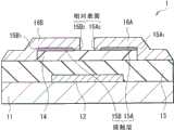
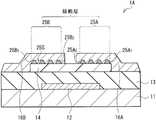
图1A示出根据本发明的第一实施例的晶体管(晶体管1)的横截面结构。晶体管1是使用有机半导体材料用于半导体层的场效应晶体管,即有机TFT。晶体管1用作使用液晶、有机电致发光(EL)或电泳显示元件的显示装置的驱动装置。晶体管1是所谓的顶接触底栅极TFT,并且在衬底11上以下列顺序包括栅电极12、栅极绝缘层13(绝缘层)、有机半导体层14(半导体层)、接触层15A和15B、和源漏电极16A和16B。FIG. 1A shows a cross-sectional structure of a transistor (transistor 1 ) according to a first embodiment of the present invention. The
衬底11支撑栅电极12等,衬底11的表面(栅电极12一侧上的表面)具有绝缘特性。衬底11构造成使用塑料衬底,例如,该塑料衬底由聚醚砜(PES)、聚萘二甲酸乙二醇酯(PEN)、聚对苯二甲酸乙二醇酯(PET)、聚碳酸酯(PC)和聚酰亚胺(PI)形成。对于衬底11,可以使用通过用树脂覆盖金属箔(例如不锈钢(SUS))的表面而构造的衬底,或者可以使用玻璃衬底。为获得高柔性,优选使用塑料衬底或金属箔。The
栅电极12具有将栅极电压施加到晶体管1并使用栅极电压来控制有机半导体层14中的载流子密度的功能。栅电极12设置在衬底11的选择性区域中,并由单金属(例如金(Au)、铝(Al)、银(Ag)、铜(Cu)、铂(Pt)和镍(Ni))或其合金形成。栅电极12可以是包含钛(Ti)和铬(Cr)的层状体。这种层状结构能够改进衬底11或处理抗蚀剂的粘附性。栅电极12可以由其他无机导电材料、有机导电材料或碳材料。The
栅极绝缘层13设置在栅电极12和有机半导体层14之间以使得栅电极12与连接到源漏电极16A和16B的有机半导体层14绝缘。栅极绝缘层13构造成使用有机绝缘膜,例如,该有机绝缘膜由聚乙烯苯酚(PVP)、聚甲基丙烯酸甲脂(PMMA)、聚乙烯醇(PVA)和聚酰亚胺(PI)形成。栅极绝缘层13可以构造成使用无机绝缘膜,该无机绝缘膜由氧化硅(SiO2)、氧化铝(Al2O3)、氧化钽(Ta2O5)、氮化硅(SiNx)等形成。
有机半导体层14设置在栅极绝缘层13上成岛状以面对栅电极12,并且形成施加栅极电压的沟道。有机半导体层14可以由p型有机半导体材料或n型有机半导体材料形成。P型有机半导体材料的示例包括并五苯、蒽、酞菁、卟啉、噻吩基聚合物及其衍生物。n型有机半导体材料的示例包括富勒烯、氟化并五苯、聚(苯并二咪唑并苯并菲咯啉)及其衍生物。The
接触层15A和15B(第一接触层和第二接触层)彼此面对地设置在有机半导体层14上,接触层15A和15B之间具有一距离。接触层15A和15B设置在有机半导体层14及源漏电极16A和16B之间(即在载流体的移动路径中),以抑制源漏电极16A和16B及有机半导体层14之间的接触电阻。Contact layers 15A and 15B (first contact layer and second contact layer) are disposed on the
在第一实施例中,接触层15A的端表面15A1和接触层15B的端表面15B1(接触层15A和15B的与彼此面对的端表面相反的表面)分别由源漏电极16A和16B覆盖。因此,在源漏电极16A和16B的形成处理之后的处理中,接触层15A和15B受到保护。此外,因为接触层15A和15B的彼此面对的端表面(彼此面对的表面15A2和15B2)也分别由源漏电极16A和16B覆盖,接触层15A和15B更可靠地受到保护。In the first embodiment, the
接触层15A和15B中每一者是从相应的表面15A2和15B2到相应的端表面15A1和15B1连续地形成的膜。接触层15A和15B的端表面15A1和15B1基本与有机半导体层14的端表面重合,接触层15A和15B仅设置在有机半导体层14上。Each of the contact layers 15A and 15B is a film formed continuously from the
接触层15A和15B中每一者由根据有机半导体层14的导电类型和HOMO(最高占据分子轨道)能级选择的诸如氧化物、卤化物、硫化物、碳酸盐、有机分子、配合物、导电聚合物等的材料形成。当有机半导体层14由例如p型有机半导体材料形成时,接触层15A和15B可以由如下材料形成:金属氧化物(例如,MoO3、ReO3、V2O5、WO3、TiO2、AuO、Al2O3、和CuO);氧化物(例如SO3);金属卤化物(例如,CuI、SbCl5、SbF5、FeCl3、LiF、BaF2、CaF2、和MgF2);金属硫化物(例如Cu2S);卤化物(例如,AsF5、BF3、BCl3、BBr3、和PF5);金属碳酸盐(例如,CaCO3、BaCO3、和LiCO3);对苯醌类(例如,2,3,5,6-四氰基-(对氰酸)、2,3-二溴-5,6-二氰基-对苯醌、2,3-二氯-5,6-二氰基-对苯醌、2,3-二碘-5,6-二氰基-对苯醌、2,3-二氰基-对苯醌、对四溴苯醌、对四氯苯醌、对四碘苯醌、对四氟苯醌、2,5-二氯-对苯醌、2,6-二氯-对苯醌、氯冉酸、2,5-二溴-3,6-二羟对苯醌、2,5-二羟基-对苯醌、2,5-二氯-3,6-二甲基-对苯醌、2,5-二溴-3,6-二甲基-对苯醌、BTDAQ、对苯醌、2,5-二甲基-对苯醌、2,6-二甲基-对苯醌、杜烯(1,2,4,5-四甲基苯)、邻苯醌、拎四溴苯醌、邻四氯苯醌、1,4-萘醌、2,3-二氰基-5-硝基-1,4-萘醌、2,3-二氰基-1,4-萘醌、2,3-二氯-5-硝基-1,4-萘醌、2,3-二氯-1,4-萘醌、和1,4-萘醌);联苯醌类(例如,3,3’,5,5’-四溴-联苯醌、3,3’,5,5’-四氯-联苯醌、和联苯醌);TCNQ类(例如,四氰基-对苯醌二甲烷(TCNQ)、四氟-四氰基-对苯醌二甲烷(F4-TCNQ)、三氟甲基-TCNQ、2,5-二氟-TCNQ、单氟-TCNQ、TNAP、癸基-TCNQ、甲基-TCNQ、dihydrobarreleno-TCNQ、tetrahydrobarreleno-TCNQ、二甲基-TCNQ、二乙基-TCNQ、苯并-TCNQ、二甲氧基-TCNQ、BTDA-TCNQ、二乙氧基-TCNQ、四甲基-TCNQ、四氰基蒽醌基二甲烷、多硝基化合物、四硝基双酚、二硝基联苯、苦味酸、三硝基苯、2,6-二硝基酚和2,4-二硝基酚、以及其类似物);芴类(例如9-二氰基亚甲基-2,4,5,7-四硝基-芴、9-二氰基亚甲基-2,4,7-三硝基-芴、2,4,5,7-四硝基-芴酮、和2,4,7-三硝基-芴酮);苯佐卡因类(例如,(TBA)2HCTMM、(TBA)2HCDAHD、K·CF、TBA·PCA、TBA·MeOTCA、TBA·EtOTCA、TBA·PrOTCA、(TBA)2HCP、六氰基丁二烯-四氟乙烯、和1,2,4,5-四氰基苯、以及其类似物);过渡金属配合物(例如,(TPP)2Pd(dto)2、(TPP)2Pt(dto)2、(TPP)2Ni(dto)2、(TPP)2Cu(dto)2、和(TBA)2Cu(ox)2);导电聚合物(例如,PEDOT/PSS和聚苯胺)等。Each of the contact layers 15A and 15B is composed of materials such as oxides, halides, sulfides, carbonates, organic molecules, complexes, Materials such as conductive polymers are formed. When the organic semiconductor layer 14 is formed of, for example, a p-type organic semiconductor material, the contact layers 15A and 15B may be formed of the following materials: metal oxides (for example, MoO3 , ReO3 , V2 O5 , WO3 , TiO2 , AuO , Al2 O3 , and CuO); oxides (such as SO3 ); metal halides (such as CuI, SbCl5 , SbF5 , FeCl3 , LiF, BaF2 , CaF2 , and MgF2 ); metal sulfides compounds (such as Cu2 S); halides (such as AsF5 , BF3 , BCl3 , BBr3 , and PF5 ); metal carbonates (such as CaCO3 , BaCO3 , and LiCO3 ); Quinones (e.g., 2,3,5,6-tetracyano-(p-cyanic acid), 2,3-dibromo-5,6-dicyano-p-benzoquinone, 2,3-dichloro-5 ,6-dicyano-p-benzoquinone, 2,3-diiodo-5,6-dicyano-p-benzoquinone, 2,3-dicyano-p-benzoquinone, p-tetrabromobenzoquinone, p-tetra Chlorobenzoquinone, p-tetraiodobenzoquinone, p-tetrafluorobenzoquinone, 2,5-dichloro-p-benzoquinone, 2,6-dichloro-p-benzoquinone, chloranic acid, 2,5-dibromo-3 ,6-dihydroxy-p-benzoquinone, 2,5-dihydroxy-p-benzoquinone, 2,5-dichloro-3,6-dimethyl-p-benzoquinone, 2,5-dibromo-3,6- Dimethyl-p-benzoquinone, BTDAQ, p-benzoquinone, 2,5-dimethyl-p-benzoquinone, 2,6-dimethyl-p-benzoquinone, durene (1,2,4,5-tetra Toluene), o-benzoquinone, tetrabromobenzoquinone, o-tetrachlorobenzoquinone, 1,4-naphthoquinone, 2,3-dicyano-5-nitro-1,4-naphthoquinone, 2, 3-Dicyano-1,4-naphthoquinone, 2,3-dichloro-5-nitro-1,4-naphthoquinone, 2,3-dichloro-1,4-naphthoquinone, and 1,4 -naphthoquinone); diphenoquinones (for example, 3,3',5,5'-tetrabromo-diphenoquinone, 3,3',5,5'-tetrachloro-diphenoquinone, and diphenoquinone ); TCNQs (e.g., tetracyano-quinodimethane (TCNQ), tetrafluoro-tetracyano-quinodimethane (F4-TCNQ), trifluoromethyl-TCNQ, 2,5-di Fluoro-TCNQ, monofluoro-TCNQ, TNAP, decyl-TCNQ, methyl-TCNQ, dihydrobarreleno-TCNQ, tetrahydrobarreleno-TCNQ, dimethyl-TCNQ, diethyl-TCNQ, benzo-TCNQ, dimethoxy -TCNQ, BTDA-TCNQ, diethoxy-TCNQ, tetramethyl-TCNQ, tetracyanoanthraquinone dimethane, polynitro compounds, tetranitrobisphenol, dinitrobiphenyl, picric acid, three nitrobenzene, 2,6-dinitrophenol and 2,4-dinitrophenol, and their analogs); fluorenes (e.g. 9-dicyanomethylene-2,4,5,7-tetra Nitro-fluorene, 9-dicyano Methyl-2,4,7-trinitro-fluorene, 2,4,5,7-tetranitro-fluorenone, and 2,4,7-trinitro-fluorenone); benzocaines (e.g., (TBA)2 HCTMM, (TBA)2 HCDAHD, K CF, TBA PCA, TBA MeOTCA, TBA EtOTCA, TBA ProOTCA, (TBA)2 HCP, hexacyanobutadiene-tetrafluoro ethylene, and 1,2,4,5-tetracyanobenzene, and its analogs); transition metal complexes (eg, (TPP)2 Pd(dto)2 , (TPP)2 Pt(dto)2 , ( TPP)2 Ni(dto)2 , (TPP)2 Cu(dto)2 , and (TBA)2 Cu(ox)2 ); conductive polymers (eg, PEDOT/PSS and polyaniline), etc.
当有机半导体层14由例如n型有机半导体材料形成时,接触层15A和15B可以由下列材料形成:金属(例如Li和Cs);金属碳酸盐(例如Cs2CO3和Rb2CO3);芳烃(例如,并四苯、二萘嵌苯、蔥、晕苯、并五苯、苯并菲、菲、萘、对二甲氧基苯、红荧烯、和六甲氧基三亚苯、以及其类似物);TTF类(例如,HMTTF、OMTTF、TMTTF、BEDO-TTF、TTeCn-TTF、TMTSF、EDO-TTF、HMTSF、TTF、EOET-TTF、EDT-TTF、(EDO)2DBTTF、TSCn-TTF、HMTTeF、BEDT-TTF、CnTET-TTF、TTCn-TTF、TSF、和DBTTF、以及其类似物);TTT类(例如,四硫代并四苯、四硒代并四苯和四碲代并四苯);吖嗪类(例如,二苯并[c,d]-吩噻嗪、苯并[c]-吩噻嗪、吩噻嗪、N甲基吩噻嗪、二苯并[c,d]-吩硒嗪、N,N-二甲基吩嗪和吩嗪);单胺类(例如,N,N-二乙基-m-甲苯胺、N,N-二乙基苯胺、N-乙基-o-甲苯胺、二苯胺、粪臭素、吲哚、N,N-二甲基-o-甲苯胺、o-甲苯胺、m-甲苯胺、苯胺、o-氯苯胺、o-溴苯胺和p-硝基苯胺);二元胺类(例如,N,N,N',N'-四甲基-p-苯二胺、2,3,5,6-四甲基-(均四甲苯二胺)、p-苯二胺、N,N,N',N'-四甲基联苯胺、3,3',5,5'-四甲基联苯胺、3,3'-二甲基联苯胺、3,3'-二甲氧基联苯胺、联苯胺、3,3'-二溴-5,5'-二甲基联苯胺、3,3'-二氯-5,5'-二甲基联苯胺和1,6-二氨基芘);4,4',4"-三(N-3-甲基苯基-N-苯基氨基)-三苯基氨基:(m-MTDATA);4,4',4"-三(N-(2-萘基)-N-苯基氨基)-三苯基氨基:(2TNATA);α-NDP;酞菁铜;1,4,6,8-四二甲基氨基芘;1,6-二硫代芘;十甲基二茂铁;二茂铁等。When the organic semiconductor layer 14 is formed of, for example, an n-type organic semiconductor material, the contact layers 15A and 15B may be formed of the following materials: metals (such as Li and Cs); metal carbonates (such as Cs2 CO3 and Rb2 CO3 ) Aromatic hydrocarbons (for example, tetracene, perylene, onion, coronene, pentacene, triphenylene, phenanthrene, naphthalene, p-dimethoxybenzene, rubrene, and hexamethoxytriphenylene, and and their analogs); TTFs (e.g., HMTTF, OMTTF, TMTTF, BEDO-TTF, TTeCn-TTF, TMTSF, EDO-TTF, HMTSF, TTF, EOET-TTF, EDT-TTF, (EDO)2 DBTTF, TSCn- TTF, HMTTeF, BEDT-TTF, CnTET-TTF, TTCn-TTF, TSF, and DBTTF, and their analogs); TTTs (e.g., tetrathiatetracene, tetraselenotetracene, and tetratetracene tetraphenyl); azines (e.g., dibenzo[c,d]-phenothiazine, benzo[c]-phenothiazine, phenothiazine, N-methylphenothiazine, dibenzo[c, d]-phenoselenazine, N,N-dimethylphenazine and phenazine); monoamines (e.g., N,N-diethyl-m-toluidine, N,N-diethylaniline, N -Ethyl-o-toluidine, diphenylamine, skatole, indole, N,N-dimethyl-o-toluidine, o-toluidine, m-toluidine, aniline, o-chloroaniline, o- bromoaniline and p-nitroaniline); diamines (e.g., N,N,N',N'-tetramethyl-p-phenylenediamine, 2,3,5,6-tetramethyl-( duretylenediamine), p-phenylenediamine, N,N,N',N'-tetramethylbenzidine, 3,3',5,5'-tetramethylbenzidine, 3,3'- Dimethylbenzidine, 3,3'-dimethoxybenzidine, benzidine, 3,3'-dibromo-5,5'-dimethylbenzidine, 3,3'-dichloro-5, 5'-dimethylbenzidine and 1,6-diaminopyrene); 4,4',4"-tris(N-3-methylphenyl-N-phenylamino)-triphenylamino:( m-MTDATA); 4,4',4"-tris(N-(2-naphthyl)-N-phenylamino)-triphenylamino:(2TNATA);α-NDP; copper phthalocyanine; 1, 4,6,8-tetradimethylaminopyrene; 1,6-dithiopyrene; decamethylferrocene; ferrocene, etc.
由上述材料形成的接触层15A和15B中的每一者的厚度例如约几nm到约30nm。如此提供的薄接触层15A和15B抑制沿竖直方向(厚度方向)的电阻。The thickness of each of
源漏电极16A和16B分别经由接触层15A和15B电连接到有机半导体层14。源漏电极16A和16B的相应的端部(源漏电极16A和16B的与彼此面对的部分相反的相应端部上)经由接触层15A和15B的端表面15A1和15A2以及有机半导体层14的端表面而与栅极绝缘层13接触。源漏电极16A和16B的彼此面对的部分经由接触层15A和15B的彼此面对的相应表面15A2和15B2而与有机半导体层14接触。也就是说,源漏电极16A和16B各自具有直接与栅极绝缘层13接触的区域以及直接与有机半导体层14接触的区域,从而抑制源漏电极16A和16B的电极剥落。此外,接触层15A和15B仅设置在有机半导体层14上,以使得源漏电极16A和16B大面积地直接与栅极绝缘层13接触,在围绕有机半导体层14的区域中抑制源漏电极16A和16B的接线剥落。Source-
源漏电极16A和16B中的每一者由单一金属(例如金、铝、银、铜、铂、镍和氧化铟锡(ITO))或其合金形成。与栅电极12类似,源漏电极16A和16B可以包括钛或铬作为上层或下层。这种层状结构能够实现衬底11、处理抗蚀剂或接触层15A和15B的粘附性。源漏电极16A和16B可以由包含导电微粒子的图案化导电墨构成。Each of the source-
例如,以下列方式制造晶体管1。For example,
首先,如图2A所示,栅电极12形成于衬底11上,然后形成栅极绝缘层13以覆盖栅电极12。具体地,首先,通过蒸发、溅射等在衬底11的整个表面上形成栅电极12的导电膜,然后例如利用光刻在导电膜上形成光阻剂的图案。之后,利用由光阻剂形成的图案作为掩模来对导电膜进行蚀刻和图案化。结果,形成栅电极12。可以通过印刷方法(例如丝网印刷、凹版印刷和喷墨印刷)来形成栅电极12。随后,利用涂覆方法在衬底11的整个表面上形成由有机绝缘材料制成的栅极绝缘层13,涂覆方法包括印刷方法,例如,旋转涂覆、丝网印刷、凹版印刷和喷墨印刷。当栅极绝缘层13由无机绝缘材料形成时,可以使用诸如蒸发、溅射和化学气相沉积(CVD)的方法。First, as shown in FIG. 2A , a
如图2B所示,在形成栅极绝缘层13之后,在栅极绝缘层13上面对的栅电极12的位置中形成有机半导体层14。通过使用掩模的图案沉积方法、印刷方法等直接以例如经图案化的状态形成有机半导体层14。可替换地,在衬底11的整个表面上(在栅极绝缘层13上)形成有机半导体层14的由材料形成的膜之后,通过烧蚀方法等来执行图案化。否则,通过剥落方法来形成有机半导体层14。如果装置隔离不是必要的,则有机半导体层14可以设置在衬底11的整个表面上。As shown in FIG. 2B , after the
如图3A所示,在形成有机半导体层14之后,在有机半导体层14上形成接触层15A和15B。例如,通过利用掩模的图案沉积方法或印刷方法直接以图案化的状态形成接触层15A和15B。As shown in FIG. 3A , after the
随后,形成源漏电极16A和16B以覆盖接触层15A和15B、和有机半导体层14的顶表面和端表面。如图3B所示,在衬底11的整个表面上(在栅极绝缘层13、有机半导体层14和接触层15A和15B上)形成金属膜16M之后,例如通过光刻处理来对源漏电极16A和16B进行图案化。可替换地,例如通过印刷方法直接以图案化的状态形成源漏电极16A和16B。以此方式,完成晶体管1。Subsequently, source-
当晶体管1被集成时,例如在源漏电极16A和16B上形成钝化层、平坦化层、接线等。可以在栅极绝缘层13中设置连接孔,源漏电极16A和16B可以经由连接孔连接到栅极绝缘层13下方的层上的电极(例如,与栅电极12相同的层中的电极)。When the
在第一实施例中,因为接触层15A和15B的端表面15A1和15B1覆盖有源漏电极16A和16B,所以接触层15A和15B在形成源漏电极16A和16B的处理之后的处理中受到保护,相应地提高产量。下面将参照对比示例描述其细节。In the first embodiment, since the end surfaces15A1 and 15B1 of the contact layers 15A and15B are covered with the source-
图4A示出根据对比示例的晶体管100的横截面结构。与晶体管1类似,晶体管100具有底栅极顶接触结构。但是,在晶体管100中,接触层115A和115B的相应的端表面115A1和115B1与源漏电极16A和16B的相应的端表面重合,接触层115A和115B的端表面115A1和115B1被暴露出。此外,接触层115A和115B的彼此面对的表面115A2和115B2与源漏电极16A和16B的彼此面对的表面重合,接触层115A和115B的表面115A2和115B2也被暴露出。FIG. 4A shows a cross-sectional structure of a
如图4B所示,在这种晶体管100中,接触层115A和115B的端表面115A1和115B1和表面115A2和115B2在形成源漏电极16A和16B时或随后的处理中会受到无意的侧蚀刻,相应地,会产生源漏电极16A和16B的电极剥落或接触失效。由于电极剥落和接触失效,降低了制造晶体管100的产量。As shown in FIG. 4B , in such a
在制造顶接触型晶体管时,水溶液或水通常用于防止有机半导体层受到有机溶剂影响而恶化。但是,接触层的很多材料溶于水(例如,MoO3、WO3、V2O5、FeCl3和PEDOT/PSS)。此外,接触层具有小厚度以抑制电阻。因此,接触层在制造中易于受到例如用于抗蚀剂剥落处理的碱性水溶液或水蚀刻。例如,作为接触层的材料的MoO3即使具有50nm的厚度也可在约三秒内溶解在纯水中。When fabricating a top-contact transistor, an aqueous solution or water is generally used to prevent organic semiconductor layers from being deteriorated by organic solvents. However, many materials of the contact layer are soluble in water (eg,MoO3 ,WO3 ,V2O5 ,FeCl3, andPEDOT /PSS). In addition, the contact layer has a small thickness to suppress resistance. Therefore, the contact layer is susceptible to etching by, for example, an alkaline aqueous solution or water used for resist peeling treatment during manufacture. For example, MoO3 as a material of the contact layer can be dissolved in pure water in about three seconds even with a thickness of 50 nm.
为制造晶体管100,在形成岛形的有机半导体层14之后,接触层115A和115B的材料膜和将作为源漏电极16A和16B的金属膜顺序地形成并同时受到图案化。具体地,接触层115A和115B的端表面115A1和115B1以及彼此面对的表面115A2和115B2分别与源漏电极16A和16B的端表面和彼此面对的表面重合,从而暴露出接触层115A和115B的端表面115A1和115B1和表面115A2和115B2。因此,接触层115A和115B会受到在形成源漏电极16A和16B时或在后续处理中使用的碱性水溶液或水的侧蚀刻。具体地,当实现晶体管100的集成或小型化时,接触层115A和115B很容易受到侧蚀刻。To manufacture
此外,在晶体管100中,接触层115A和115B设置在源漏电极16A和16B的整个下表面上,源漏电极16A和16B没有与有机半导体层14和栅极绝缘层13直接接触的区域。因此,如果有机半导体层14与接触层115A和115B之间的粘附性、接触层115A和115B与源漏电极16A和16B之间的粘附性、或接触层115A和115B与栅极绝缘层13之间的粘附性低,则会产生源漏电极16A和16B的电极剥落。Furthermore, in
相反,在第一实施例中,接触层15A和15B的端表面15A1和15B1分别覆盖有源漏电极16A和16B,以保护接触层15A和15B不受到在形成源漏电极16A和16B时或在形成上层(例如钝化层)时使用的水溶液或水的影响。相应地,由接触层15A和15B的侧蚀刻引起的源漏电极16A和16B的电极剥落和接触失效受到抑制,因此,能够实现改进制造的产量。此外,与接触层15A和15B的端表面15A1和15B1一样,接触层15A和15B的彼此面对的表面15A2和15B2也覆盖有源漏电极16A和16B。因此,更可靠地防止对接触层15A和15B的侧蚀刻。On the contrary, in the first embodiment, the end surfaces 15A1 and 15B1 of the contact layers15A and15B are covered with the source-
此外,在晶体管1中,源漏电极16A和16B的端部与栅极绝缘层13接触,源漏电极16A和16B的彼此面对的部分与有机半导体层14接触。相应地,接触层15A和15B与有机半导体层14之间的粘附性、接触层15A和15B与源漏电极16A和16B之间的粘附性、或接触层15A和15B与栅极绝缘层13之间的粘附性低,源漏电极16A和16B的电极剥落也受到抑制。Further, in
此外,因为接触层15A和15B仅设置在有机半导体层14上,栅极绝缘层13与源漏电极16A和16B直接接触的区域较大。因此,即使接触层15A和15B的粘附性低,也可以防止源漏电极16A和16B的接线剥落。此外,当在栅极绝缘层13中设置连接孔、并且源漏电极16A和16B经由连接孔连接到栅极绝缘层13下方的层上的电极时,接触层15A和15B不会阻挡连接。Furthermore, since the contact layers 15A and 15B are provided only on the
在第一实施例的晶体管1中,当向栅电极12提供预定电势时,在有机半导体层14的沟道中产生电场,电流在源漏电极16A和16B之间流动。也就是说,晶体管1用作所谓的场效应晶体管。在这种情况下,因为接触层15A和15B的端表面15A1和15B1分别覆盖有源漏电极16A和16B,防止接触层15A和15B的侧蚀刻。In
如上所述,在第一实施例中,接触层15A和15B的端表面15A1和15B1分别覆盖有源漏电极16A和16B。因此,防止接触层15A和15B受到侧蚀刻,并且抑制源漏电极16A和16B的电极剥落和接触失效。结果,防止由对接触层15A和15B的侧蚀刻引起的制造故障,因此提高产量。此外,与接触层15A和15B的端表面15A1和15B1一样,接触层15A和15B的彼此面对的表面15A2和15B2也分别覆盖有源漏电极16A和16B。因此,更可靠地防止对接触层15A和15B的侧蚀刻。As described above, in the first embodiment, the end surfaces 15A1 and 15B1 of the contact layers 15A and 15B are covered with the source-
此外,源漏电极16A和16B的端部各自具有直接与栅极绝缘层13接触的区域,并且源漏电极16A和16B的彼此面对的表面各自具有直接与有机半导体层14接触的区域。因此,当接触层15A和15B的粘附性低时,也可以防止源漏电极16A和16B的电极剥落。Further, end portions of source-
下面将描述第一实施例和其他实施例的修改形式,而相同的附图标记用于与第一实施例表示基本相同的组件,将适当地省略对其的描述。Modifications of the first embodiment and other embodiments will be described below, while the same reference numerals are used for substantially the same components as those of the first embodiment, and descriptions thereof will be appropriately omitted.
[修改形式1][Modification 1]
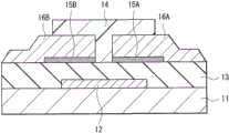
图5示出根据第一实施例的修改形式1的晶体管(晶体管1A)的横截面结构。晶体管1A与第一实施例的晶体管1的不同之处在于接触层25A和25B处于非连续状态。除此之外,晶体管1A的构造与晶体管1类似,并且晶体管1A的功能和效果也与晶体管1类似。FIG. 5 shows a cross-sectional structure of a transistor (
接触层25A和25B在从接触层25A和25B的彼此面对的表面25A2和25B2到接触层25A和25B的端表面25A1和25B1的相应区域中具有多个微小间隙25S,即,接触层25A和25B设置成非连续状态。也就是说,接触层25A和25B分散成中间具有间隙25S的颗粒状态。因此,即使在接触层25A和25B的彼此面对的表面25A2和25B2没有被源漏电极16A和16B覆盖的情况下,通过间隙25S抑制水溶液或水从表面25A2和25B2渗透。也就是说,保护接触层25A和25B的将作为载流子移动路径的部分。例如,每个间隙25S的尺寸是10到100nm。The contact layers 25A and 25B have a plurality of
例如,以下列方式制造晶体管1A。For example, the
首先,如图6A所示,直到栅极绝缘层13的层形成为晶体管1。随后,如图6B所示,在栅极绝缘层13上形成有机半导体层14和接触层25A和25B。通过使用掩模的图案沉积方法或印刷方法以下列顺序相继直接地对有机半导体层14和接触层25A和25B进行图案化。可替换地,在衬底11的整个表面上由有机半导体层14的材料形成的膜以及在衬底11的整个表面上处于非连续状态的接触层25A和25B以此顺序形成,然后通过激光烧蚀方法等同时对有机半导体层14和接触层25A和25B进行图案化。可以通过剥落方法形成有机半导体层14和接触层25A和25B。当通过将真空膜形成速率设置为低并将膜形成时间设置为短来结束真空膜形成时,在膜发展成连续膜之前,接触层25A和25B处于非连续状态,即,形成具有多个间隙25S的接触层25A和25B。通过图案沉积方法或印刷方法直接形成非连续图案。First, as shown in FIG. 6A , the layers up to the
在形成接触层25A和25B之后,如图6C所示形成源漏电极16A和16B。在衬底11的整个表面上形成金属膜(例如,金属膜16M)之后,可以通过光刻处理来对源漏电极16A和16B进行图案化。可替换地,可以通过印刷方法直接形成源漏电极16A和16B的图案。After the contact layers 25A and 25B are formed, source-
如果关断电流足够,则可以留下源漏电极16A和源漏电极16B之间的间隙中的接触层25A和25B(图6C)。如果关断电流不足,则通过蚀刻去除间隙中的接触层25A和25B(图5)。这时,因为接触层25A和25B具有间隙25S,通过间隙25S阻挡在蚀刻中使用的水或水溶液的渗透,不会腐蚀接触层25A和25B的将作为载流子移动路径的部分(源漏电极16A和16B与有机半导体层14之间的接触层25A和25B的部分)。If the off current is sufficient,
[第二实施例][Second embodiment]
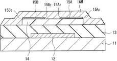
图7A示出根据本发明的第二实施例的晶体管(晶体管2)的横截面结构。晶体管2与第一实施例的晶体管1的不同之处在于接触层35A和35B各自经过有机半导体层14的端表面而在栅极绝缘层13上延伸。除此之外,晶体管2的构造与晶体管1类似,并且晶体管2的功能和效果也与晶体管1类似。FIG. 7A shows a cross-sectional structure of a transistor (transistor 2 ) according to a second embodiment of the present invention.
接触层35A和35B中每一者都是连续膜,并且从有机半导体层14的顶表面延伸经过有机半导体层14的端表面而到达栅极绝缘层13上。接触层35A和35B相距一距离。面对表面35B2的表面35A2与端表面35A1覆盖有源漏电极16A,表面35B2和端表面35B1覆盖有源漏电极16B。接触层35A和35B中每一者可以连续地从有机半导体层14上形成到栅极绝缘层13上(图7A),或者可以被有机半导体层14切割分层,即,可以分成位于有机半导体层14上的部分和位于栅极绝缘层13上的部分,如图7B所示。Each of the contact layers 35A and 35B is a continuous film, and extends from the top surface of the
[修改形式2][Modification 2]
图8示出根据修改形式2的晶体管(晶体管2A)的横截面结构。晶体管2A与第二实施例中的晶体管2的不同之处在于接触层45A和45B处于非连续状态。除此之外,晶体管2A的构造与晶体管2类似,并且晶体管2A的功能和效果也与晶体管2类似。FIG. 8 shows a cross-sectional structure of a transistor (
接触层45A和45B在相应的彼此面对的表面45A2和45B2与相应的端表面45A1和45B1之间具有多个微小间隙45S,并且接触层45A和45B以非连续状态设置在有机半导体层14的顶表面上和栅极绝缘层13上。接触层45A和45B相距一距离。表面45A2和端表面45A1覆盖有源漏电极16A,表面45B2和端表面45B1覆盖有源漏电极16B。因为接触层45A和45B中每一者都是非连续层,即使接触层45A和45B的彼此面对的表面45A2和45B2分别没有被源漏电极16A和16B覆盖,也可通过间隙45S阻止水溶液或水从表面45A2和45B2渗透。非连续状态的接触层45A和45B形成为接触层25A和25B。当关断电流足够时,接触层45A和45B可以存在于源漏电极16A和源漏电极16B之间的间隙中。The contact layers 45A and 45B have a plurality of
[应用示例1-1][Application example 1-1]
图9示出包括作为驱动装置的任意晶体管1、1A、2和2A的显示装置(显示装置90)的电路构造。例如,显示装置90是液晶显示装置、有机EL显示装置、或电子纸显示装置,并且包括多个像素10和驱动像素10的各种驱动电路,像素10以矩阵形式设置在驱动面板91上的显示区域110中。对于驱动电路,作为图像显示的驱动器的信号线驱动电路120和扫描线驱动电路130、和像素驱动电路150设置在驱动面板91上。密封面板(未示出)连接到驱动面板91,像素10和驱动电路被密封面板所密封。FIG. 9 shows a circuit configuration of a display device (display device 90 ) including
图10是像素驱动电路150的等效电路图。像素驱动电路150是具有作为晶体管1、1A、2和2A中任一者的晶体管Tr1和Tr2的有源驱动电路。电容Cs设置在晶体管Tr1和Tr2之间,像素10与第一电力线(Vcc)和第二电力线(GND)之间的晶体管Tr1串联连接。在这种像素驱动电路150中,多个信号线120A沿列方向布置,多个扫描线130A沿行方向布置。每个信号线120A连接到信号线驱动电路120,像素信号从信号线驱动电路120经由信号线120A被供应到晶体管Tr2的源电极。每个扫描线130A连接到扫描线驱动电路130,扫描信号顺序地从扫描线驱动电路130经由扫描线130A被供应到晶体管Tr2的栅电极。在显示装置中,晶体管Tr1和Tr2由实施例的晶体管1、1A、2和2A中任一者构成。因此,通过晶体管Tr1和Tr2的有利TFT特性执行高质量显示。例如,这种显示装置90可以安装在应用示例1至6的电子设备上。FIG. 10 is an equivalent circuit diagram of the
此外,在实施例等中,举例说明使用有机半导体材料来构造半导体层的情况。可替换地,可以使用无机材料(例如硅和氧化物半导体)来构造半导体层。Furthermore, in the embodiments and the like, a case where an organic semiconductor material is used to configure a semiconductor layer is exemplified. Alternatively, inorganic materials such as silicon and oxide semiconductors may be used to configure the semiconductor layer.
此外,例如,每个层的材料和厚度、或者该层的膜形成方法和膜形成条件不限于实施例等中所述的这些。可以使用其他材料和厚度、或者其他膜形成方法和膜形成条件。In addition, for example, the material and thickness of each layer, or the film formation method and film formation conditions of the layer are not limited to those described in Examples and the like. Other materials and thicknesses, or other film forming methods and film forming conditions may be used.
[第三实施例][Third embodiment]
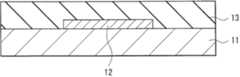
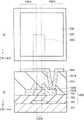
图11示出根据本发明的第三实施例的显示装置(显示装置1001)的横截面结构的一部分。显示装置1001是有源矩阵显示装置,并且在衬底1011上以下列顺序包括作为驱动装置的晶体管1020、层间绝缘膜1031、像素电极1041(电极)、显示层1051、公共电极1061和对衬底1071。晶体管1020是底栅极顶接触有机TFT,并且从衬底1011一侧以下列顺序包括栅电极1021、栅极绝缘膜1022、半导体膜1023、和源漏电极1024A和1024B。应注意,图11示意性示出显示装置1001的结构,在某些情况下显示装置1001的尺寸和形状与实际尺寸和实际形状不同。FIG. 11 shows part of a cross-sectional structure of a display device (display device 1001 ) according to a third embodiment of the present invention. The
例如,衬底1011由无机材料(例如玻璃、石英、硅和砷化镓);由聚对苯二甲酸乙二醇酯(PET)、聚萘二甲酸乙二醇酯(PEN)、聚醚砜(PES)、聚醚酰亚胺、聚醚醚铜(PEEK)、聚苯硫醚、聚芳酯、聚酰亚胺、聚酰胺、聚碳酸酯(PC)、三乙酸纤维素、聚烯烃、聚苯乙烯、聚乙烯、聚丙烯、聚甲基丙烯酸甲酯(PMMA)、聚氯乙烯、聚偏二氯乙烯、环氧树脂、酚醛树脂、脲醛树脂、三氯氰胺树脂、硅树脂、丙烯酸树脂等形成的膜;或金属箔形成。衬底1011可以是由硅等形成刚性衬底,或者可以是由薄玻璃、上述塑料膜等形成的柔性衬底。如果衬底1011是柔性衬底,可实现可折叠的柔性显示装置。衬底1011可以具有导电性。For example, the
栅电极1021将栅电压供应至晶体管1020,并使用栅电压来控制半导体膜1023的载流子密度以形成沟道区域(之后描述的图12中的沟道区域1023A)。栅电极1021设置在衬底1011的选择区域中而具有例如10nm至1000nm的厚度(沿Z轴方向)。栅电极1021由单金属(例如金(Au)、铝(Al)、铜(Cu)、铂(Pt)、钛(Ti)、钌(Ru)、钼(Mo)、钨(W)、镍(Ni)、铝(Al)和钽(Ta))或其合金形成。由这些金属形成的膜可以经层叠而形成栅电极1021。此外,可以使用由氧化铟锡(ITO)、氧化锌锡(IZO)、氧化锌(ZnO)等形成的氧化物膜,或者使用导电碳化材料(例如碳纳米管和石墨烯)来构造栅电极1021。The
栅极绝缘膜1022设置在栅电极1021和半导体膜1023之间,以使得栅电极1021与电连接到源漏电极1024A和1024B的半导体膜1023绝缘。例如,栅极绝缘膜1022的厚度约10nm到约1000nm。使用由聚乙烯吡咯烷酮(PVP)、聚乙烯苯酚、PMMA、聚乙烯醇(PVA)、PI等形成的有机绝缘膜来构造栅极绝缘膜1022。可以使用由二氧化硅(SiO2)、二氧化钛(TiO2)、氧化铝(Al2O3)、氧化钽(Ta2O5)等形成的氧化物膜,或者由氮化硅(SiNx)等形成的氮化物膜,来构造栅极绝缘膜1022。A
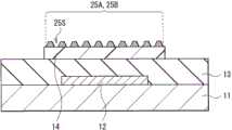
如图12所示,半导体膜1023在栅极绝缘膜1022上设置成岛形,并且在源漏电极1024A和源漏电极1024B之间具有沟道区域1023A。在第三实施例中,如图12的(A)所示,半导体膜1023覆盖有像素电极1041,具有矩形平面形状的半导体膜1023的所有四个侧边定位成在像素电极1041的平面区域内面对像素电极1041。因此,半导体膜1023的沟道区域1023A设置在更靠近像素电极1041的中心部分的位置上,改进沟道区域1023A的各向同性。因此,能够改进晶体管1020的TFT特性。图12的(B)示出沿着图12的(A)的B-B线获得的横截面结构。As shown in FIG. 12 , the
为进一步改进沟道区域1023A的各向同性,源漏电极1024A和1024B还优选地覆盖有像素电极1041。但是,在像素电极1041的平面区域内,至少沟道区域1023A的彼此面对的侧边定位成面对像素电极1041。此外,如图13和图14所示,尽管在像素电极1041的平面区域内半导体膜1023的构造平面形状的所有侧边(或沟道区域1023A)优选定位成面对像素电极1041,在像素电极1041的平面区域内半导体膜1023的至少一对彼此面对的侧边可以定位成面对像素电极1041。可替换地,在像素电极1041的平面区域内,一对沿着沟道长度(X轴)方向(图13)或沿着沟道宽度(Y轴)方向(图14)彼此面对的侧边可以定位成面对像素电极1041。如果半导体膜1023具有四边形形状,则半导体膜1023的三个侧边设置在像素电极1041的平面区域内。To further improve the isotropy of the
半导体膜1023由有机半导体材料形成,具体地,例如,半导体膜1023由多环芳烃(例如,并五苯、蔥和红荧烯)、低分子化合物(例如四氰基对苯醌二甲烷(TCNQ))或高分子化合物(例如,聚乙烯、聚(3-己基噻吩)(P3HT)、聚(对苯乙烯撑)(PPV))形成。半导体膜1023的厚度约1nm至约1000nm。The
一对源漏电极1024A和1024B设置在半导体膜1023上,并同将与其电连接的半导体膜1023接触。对于源漏电极1024A和1024B的材料,可以使用与栅电极1021类似的材料,因此例如使用(由金、银、铜、铝等形成的)金属膜、(由ITO等形成的)氧化物膜、或(由碳纳米管、石墨烯等形成的)导电碳化材料膜来构造源漏电极1024A和1024B。源漏电极1024A和1024B中每一者的厚度例如约10nm至约1000nm。A pair of source-
层间绝缘膜1031使具有晶体管1020的衬底1011的表面平坦化,并且层间绝缘膜1031具有连接孔1031H,连接孔1031H在源漏电极1024B(晶体管1020)和像素电极1041之间进行导电。例如,层间绝缘膜1031可以由氧化硅、氮化硅、氧化铝、氮化铝(AlN)、氧化钽或氮氧化铝(AlOxN1-x,其中X=0.01至0.2)。诸如PVA、聚乙烯基酚、酚醛树脂、丙烯酸树脂和氟基树脂的有机材料可以用于层间绝缘膜1031。The
像素电极1041设置在每个像素的层间绝缘膜1031上,并且将电压施加到像素电极1041和公共电极1061之间的显示层1051。在显示装置1001的平面视图中,像素电极1041的面积大于沟道区域1023A的面积,如上所述在像素电极1041的平面区域内沟道区域1023A的所有侧边定位成面对像素电极1041。也就是说,像素电极1041包括在沟道区域1023A外部的非重叠区域(非重叠区域1041A和1041B)。非重叠区域1041A和1041B是朝向外侧悬挂在沟道区域1023A之外的区域。非重叠区域1041A是沿着沟道长度方向彼此面对的一对区域,沟道区域1023A位于这一对区域之间;非重叠区域1041B是沿着沟道宽度方向彼此面对的一对区域,沟道区域1023A位于这一对区域之间。尽管像素电极1041优选沿两个方向具有非重叠区域1041A和1041B(图12),但是可以具有非重叠区域1041A和1041B中的一者(图13和图14)。The
像素电极1041具有四边形平面形状(例如,正方形、矩形和平行四边形),并且使用(由金、银、铜、铝等形成的)金属膜、(由ITO等形成的)氧化物膜、或(由碳纳米管、石墨烯等形成的)导电碳化材料膜来构造像素电极1041。如图15所示,像素电极1041可以具有狭缝1041S,以防止与接线(例如信号线)重叠。像素电极1041的厚度例如约10nm至约1000nm。The
显示层1051设置在像素电极1041和公共电极1061之间,并且受到每个像素的晶体管1020驱动。例如,显示层1051由液晶层、有机EL层、无机EL层、或电泳显示元件构成。例如,公共电极1061由像素共用,并且设置在对衬底1071的一个表面上。公共电极1061由透明导电材料(例如ITO)形成,并且具有例如约10nm至约1000nm的厚度。The
例如,使用与衬底1011类似的材料来构造对衬底1071。在显示装置1001中,图像显示在对衬底1071一侧上。可以在对衬底1071上设置用于防止水渗透到显示层1051的防水膜、用于防止外界光的反射的光学功能膜等。For example, the
例如,以下列方式制造显示装置1001。For example, the
首先,利用真空等离子体技术(例如蒸发和溅射)在衬底1011的整个表面上形成导电膜,然后通过光刻或蚀刻对形成的导电膜进行图案化以形成期望形状的栅电极1021。可以通过涂覆和印刷方法(例如丝网印刷和喷墨方法)来形成导电膜。在衬底1011的表面上的粗糙度大的情况下,可以在形成栅电极1021之前对衬底1011执行化学抛光处理或平坦化处理(例如形成平坦化膜)。应注意,衬底1011的表面的粗糙度大的情况表示例如在衬底1011的表面上存在引起形成于衬底1011上的膜不连续的大凹凸物或急倾凹凸物的情况。First, a conductive film is formed on the entire surface of the
在形成栅电极1021之后,例如通过蒸发或溅射在衬底1011和栅电极1021上形成氧化硅膜,以形成栅极绝缘膜1022。可以通过涂覆方法(例如旋转涂覆和狭缝涂覆)使用有机绝缘材料来形成栅极绝缘膜1022。在形成栅极绝缘膜1022之后,通过使用金属掩模的真空沉积方法或涂覆方法(例如旋转涂覆和喷墨方法)来图案化并形成半导体膜1023。当半导体膜1023的有机半导体材料是低分子化合物时优选使用真空沉积方法,而当半导体膜1023的有机半导体材料是可溶的高分子化合物时优选使用涂覆和印刷方法。After forming
随后,利用真空等离子体技术(例如蒸发和溅射)在栅极绝缘膜1022和半导体膜1023上形成导电膜。然后,通过光刻和蚀刻对导电膜进行图案化以形成一对源漏电极1024A和1024B。相应地,晶体管1020形成于衬底1011上。可以通过涂覆和印刷方法(例如丝网印刷和喷墨方法)形成构造源漏电极1024A和1024B的导电膜,作为栅极绝缘膜1022。Subsequently, a conductive film is formed on the
随后,在晶体管1020上形成层间绝缘膜1031,然后利用半导体光刻和蚀刻来形成连接孔1031H。例如,当层间绝缘膜1031的绝缘材料可溶时,可以通过旋转涂覆或丝网印刷来形成层间绝缘膜1031,而当绝缘材料不可溶时,例如可以通过溅射来形成层间绝缘膜1031。Subsequently, an
在层间绝缘膜1031中形成连接孔1031H之后,对每个像素执行图案化以在层间绝缘膜1031上形成像素电极1041,晶体管1020电连接到像素电极1041。这时,像素电极1041设置在晶体管1020上以具有非重叠区域1041A和1041B。例如,可以按照与源漏电极1024A和1024B类似的方式形成像素电极1041。After the
在形成像素电极1041之后,显示层1051形成于像素电极1041上。之后,使得包括公共电极1061的对衬底1071面对形成到具有显示层1051的衬底1011。以此方式,完成图11所示的显示装置1001。After the
在根据第三实施例的显示装置1001中,在平面视图中沟道区域1023A的所有侧边定位在像素电极1041内。结果,改进晶体管1020的TFT特性。下面将参照对比示例描述其细节。In the
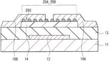
图16示出根据对比示例的显示装置(显示装置1100)的结构,其中图16的(A)示出显示装置1100的平面结构,图16的(B)示出沿着图16的(A)中的B-B线获得的横截面结构。在显示装置1100中,在平面视图中沟道区域1023A的彼此正交的(沿X轴方向和Y轴方向的)两个侧边与像素电极(像素电极1141)的两个侧边重叠。也就是说,沟道区域1023A设置在像素电极1141的拐角处。在这种显示装置1100中,降低沟道区域1023A的各向同性,施加到沟道区域1023A的应力不均匀。结果,降低TFT特性。此外,在显示装置1100中,由于暴露于空气而易于使沟道区域1023A(半导体膜1023)恶化。FIG. 16 shows the structure of a display device (display device 1100 ) according to a comparative example, wherein (A) of FIG. 16 shows the planar structure of the
相反,在显示装置1001中,在平面视图中沟道区域1023A的所有侧边定位在像素电极1041内,即,沟道区域1023A定位在更靠近像素电极1041的中心的位置上。相应地,改进沟道区域1023A的各向同性,并使得施加到沟道区域1023A的应力均匀。结果,改进晶体管1020的TFT特性。具体地,当衬底1011是柔性衬底时,即,当显示装置1001是柔性显示装置时,增大应力的影响,以使得晶体管1020的TFT特性被有效地改进。此外,因为半导体膜1023大部分覆盖有像素电极1041,所有由于空气侵扰引起的沟道区域1023A的恶化受到抑制。In contrast, in the
图17A示出显示装置1001(实线)和显示装置1100(虚线)中每一者的晶体管的传输特性,水平轴表示栅极电压(VGS),竖直轴表示漏极电流(ID)。上升的栅极电压VGS在显示装置1100中为约8V,而在显示装置1001中为约3V。也就是说,通过比显示装置1100低的电压来驱动显示装置1001。17A shows the transfer characteristics of the transistors of each of the display device 1001 (solid line) and the display device 1100 (dashed line), with the horizontal axis representing the gate voltage (VGS ) and the vertical axis representing the drain current (ID ) . The raised gate voltage VGS is about 8V in the
图17B是示出在显示装置1100的栅极电压VGS例如按照显示装置1001的电压的减少量(5V)移动的状态下显示装置1100和1001的漏极电流(ID)的对比的示图。从附图可明显看出,显示装置1001的漏极电流ID与显示装置1100的漏极电流相比不降低。因此,确认可通过更低的电压来驱动显示装置1001,而不会降低晶体管1020的最大场效应迁移率。17B is a graph showing a comparison of drain currents (ID ) of the
在显示装置1001中,沟道区域1023A设置在更靠近像素电极1041的中心的位置上,以使得晶体管1020的TFT特性可以改进。图18A和18B示出一对非重叠区域1041A中的一者(在源漏电极1024A一侧)的上升电压(VT0)和长度(L)之间的关系,其中当漏极电流ID是10-8A时VT0是栅极电压VGS。应注意,一对非重叠区域1041A中另一者的长度、以及一对非重叠区域1041B中每一者的长度(图12的(B))各自等于或大于L。也就是说,在沟道区域1023A的所有侧边定位在像素电极1041的平面区域内的状态下执行测量。这时,上升电压VT0随着长度L增大而逐渐降低,当L是200至300μm时,VT0达到0V(图18B)。相应地,沟道区域1023A设置在更靠近像素电极1041的中心的位置处,以使得上升电压VT0接近0V。In the
如上所述,在第三实施例的显示装置1001中,在像素电极1041的平面区域内,至少沟道区域1023A的彼此面对的一对侧边定位成面对像素电极1041。因此,改进沟道区域1023A的各向同性,并且改进晶体管1020的TFT特性。因此,能够通过更低的功率来驱动显示装置1001。As described above, in the
在下文中,尽管将描述第三实施例的修改形式,但是相同的附图标记用于表示与第三实施例基本相同的组件,并且适当地省略对其的描述。Hereinafter, although a modified form of the third embodiment will be described, the same reference numerals are used to denote substantially the same components as those of the third embodiment, and descriptions thereof are appropriately omitted.
[修改形式3][Modification 3]
图19示出根据第三实施例的修改形式3的显示装置(显示装置1001A)的主要部分的结构。图19的(A)示出显示装置1001A的平面结构,图19的(B)示出沿着图19的(A)中的B-B线获得的横截面结构。显示装置1001A包括保持电容1050。除此之外,显示装置1001A的结构与第三实施例的显示装置1001类似,并且显示装置1001A的功能和效果也与显示装置1001类似。FIG. 19 shows the structure of a main part of a display device (
保持电容1050包括下电极1021C(第二电极)和上电极1024C(第三电极),栅极绝缘膜1022设置在下电极1021C和上电极1024C之间。下电极1021C设置在与栅电极1021相同的层中,上电极1024C与源漏电极1024B形成整体。与源漏电极1024A和1024B设置在同一层中的接线1024D连接到源漏电极1024A。例如,接线1024D是信号线。在显示装置1001A中,保持电容1050设置在沿沟道宽度(Y轴)方向彼此面对的区域中的每一者中,半导体膜1023(沟道区域1023A)位于该彼此面对的区域之间。也就是说,上电极1024C(源漏电极1024B)从三个方向围绕半导体膜1023(图20)。相应地,因为保持电容1050(上电极1024C)设置在宽广区域上,所以电容增大。具体地,因为当显示层1051由电泳显示元件构成时需要大电容,所以优选以此方式设置保持电容1050。像素电极1041设置成覆盖整个上电极1024C。The
如图21的(A)和(B)所示,通过经由设置在栅极绝缘膜中的连接孔1022HA和1022HB电连接源漏电极1024A和接线1024D,可以由上电极1024C来围绕半导体膜1023的所有侧边(图22)。As shown in (A) and (B) of FIG. 21 , by electrically connecting the source-
当同时实施第三实施例和修改形式3以及第一实施例、修改形式1、第二实施例和修改形式2中任一者时,提供具有高可靠性的晶体管、显示装置和电子设备。When the third embodiment and modification 3 and any one of the first embodiment,
显示装置90和1001(或显示装置1001A)能够安装在下文所述的应用示例1至6中所示的电子设备上。The
[应用示例1][Application example 1]
图23A和23B各自示出电子书的外观。例如,电子书包括显示部分210、非显示部分220、和操作部分230,显示装置210由显示装置90、1001或1001A构造。操作部分230可以如图23A所示设置在与显示部分210相同的表面(前表面)上,或者可以如图23B所示设置在与显示部分210不同的表面(顶表面)上。23A and 23B each show an appearance of an electronic book. For example, an electronic book includes a display portion 210, a non-display portion 220, and an operation portion 230, and the display device 210 is configured by the
[应用示例2][Application example 2]
图24示出电视机的外观。例如,电视机包括图像显示屏部分300,图像显示屏部分300包括前面板310和滤光玻璃320,图像显示屏部分300由显示装置90、1001或1001A构造。Fig. 24 shows the appearance of a television. For example, a television includes an image
[应用示例3][Application example 3]
图25A和25B各自示出数字照相机的外观。例如,数字照相机包括用于闪光的光发射部分410、显示部分420、菜单切换装置430和快门按钮440,显示部分420由显示装置90、1001或1001A构造。25A and 25B each show the appearance of a digital camera. For example, a digital camera includes a
[应用示例4][Application example 4]
图26示出笔记本个人电脑的外观。例如,笔记本个人电脑包括主体510、用于字符等的输入操作的键盘520、和显示图像的显示部分530,显示部分530由显示装置90、1001或1001A构造。Fig. 26 shows the appearance of a notebook personal computer. For example, a notebook personal computer includes a
[应用示例5][Application example 5]
图27示出视频摄像机的外观。例如,视频摄像机包括主体610、设置在主体610的前侧表面上的用于拍摄物体的镜头620、用于拍摄的开始和停止开关630、和显示部分640。显示部分640由显示装置90、1001或1001A构造。Fig. 27 shows the appearance of a video camera. For example, a video camera includes a main body 610 , a lens 620 disposed on a front side surface of the main body 610 for photographing a subject, a start and stop switch 630 for photographing, and a display part 640 . The display portion 640 is configured by the
[应用示例6][Application example 6]
图28A至28G各自示出移动电话的外观。例如,移动电话由通过连接部分(铰链部分)730彼此连接的上壳体710和下壳体720构成,并且移动电话包括显示装置740、次显示装置750、图片光源760和摄像头770。显示装置740和/或次显示装置750由显示装置90、1001或1001A构造。28A to 28G each show an appearance of a mobile phone. For example, a mobile phone is composed of an
在前文中,尽管参照实施例和修改形式描述了本发明,但是本发明不限于此,可以进行各种修改。例如,尽管在实施例中等中描述了顶接触底栅极晶体管1、1A、2、2A等,本发明可以如图1B所示应用于底接触底栅极晶体管,或者可以应用于具有顶栅极结构的晶体管。In the foregoing, although the present invention has been described with reference to the embodiments and modified forms, the present invention is not limited thereto, and various modifications can be made. For example, although top-
例如,每个层的材料和厚度、或每个层的膜形成方法和膜形成条件不限于实施例等中所述的这些。可以使用其他材料和厚度、或者其他膜形成方法和膜形成条件。For example, the material and thickness of each layer, or the film formation method and film formation conditions of each layer are not limited to those described in Examples and the like. Other materials and thicknesses, or other film forming methods and film forming conditions may be used.
此外,在实施例等中,对晶体管1020是有机TFT的情况(即,半导体膜1023由有机半导体材料形成的情况)进行描述。可替换地,半导体膜1023可以由无机半导体材料(例如非晶硅和氧化物半导体)形成。In addition, in the embodiments and the like, description is made of the case where the
此外,在实施例等中,对晶体管1020是底栅极顶接触型TFT的情况进行描述。可替换地,晶体管1020可以是顶栅极顶接触型、顶栅极底接触型、或底栅极底接触型。Furthermore, in the embodiments and the like, the description is made on the case where the
应注意本发明可以如下构造。It should be noted that the present invention may be configured as follows.
(1)一种晶体管,其包括:(1) A transistor comprising:
栅电极;gate electrode;
面对栅电极的半导体层,绝缘层位于半导体层和栅电极之间;a semiconductor layer facing the gate electrode, with an insulating layer between the semiconductor layer and the gate electrode;
一对源漏电极,其电连接到半导体层;和a pair of source-drain electrodes electrically connected to the semiconductor layer; and
接触层,其设置在一对源漏电极中的每一者与半导体层之间的载流子移动路径中,接触层的端表面被源漏电极覆盖。A contact layer is provided in a carrier movement path between each of the pair of source-drain electrodes and the semiconductor layer, an end surface of the contact layer being covered with the source-drain electrodes.
(2)根据(1)的晶体管,其中,接触层设置在半导体层和一对源漏电极中的每一者之间。(2) The transistor according to (1), wherein the contact layer is provided between the semiconductor layer and each of the pair of source-drain electrodes.
(3)根据(1)或(2)的晶体管,其中(3) The transistor according to (1) or (2), wherein
接触层包括彼此面对的一对第一接触层和第二接触层,第一接触层和第二接触层设置在半导体层和一对源漏电极中的每一者之间,并且The contact layer includes a pair of first and second contact layers facing each other, the first and second contact layers being disposed between the semiconductor layer and each of the pair of source-drain electrodes, and
彼此面对的第一接触层的表面和第二接触层的表面也被源漏电极覆盖。The surface of the first contact layer and the surface of the second contact layer facing each other are also covered with the source-drain electrodes.
(4)根据(1)至(3)中任一者的晶体管,其中(4) The transistor according to any one of (1) to (3), wherein
接触层设置在半导体层上,并且a contact layer is disposed on the semiconductor layer, and
一对源漏电极与绝缘层接触。A pair of source-drain electrodes is in contact with the insulating layer.
(5)根据(1)至(4)中任一者的晶体管,其中,接触层处于具有多个间隙的非连续状态。(5) The transistor according to any one of (1) to (4), wherein the contact layer is in a discontinuous state with a plurality of gaps.
(6)根据(5)的晶体管,其中,通过在接触层发展成连续膜之前完成真空膜形成来形成处于非连续状态的接触层。(6) The transistor according to (5), wherein the contact layer in a discontinuous state is formed by completing vacuum film formation before the contact layer develops into a continuous film.
(7)根据(1)至(4)中任一者的晶体管,其中,接触层是连续膜。(7) The transistor according to any one of (1) to (4), wherein the contact layer is a continuous film.
(8)根据(1)至(7)中任一者的晶体管,其中,接触层延伸经过半导体层的端表面而到达半导体层的两侧上。(8) The transistor according to any one of (1) to (7), wherein the contact layer extends past the end surface of the semiconductor layer onto both sides of the semiconductor layer.
(9)一种包括多个像素和驱动多个像素的晶体管的显示装置,晶体管包括:(9) A display device comprising a plurality of pixels and a transistor for driving the plurality of pixels, the transistor comprising:
栅电极;gate electrode;
面对栅电极的半导体层,绝缘层位于半导体层和栅电极之间;a semiconductor layer facing the gate electrode, with an insulating layer between the semiconductor layer and the gate electrode;
一对源漏电极,其电连接到半导体层;和a pair of source-drain electrodes electrically connected to the semiconductor layer; and
接触层,其设置在一对源漏电极中的每一者与半导体层之间的载流子移动路径中,接触层的端表面被源漏电极覆盖。A contact layer is provided in a carrier movement path between each of the pair of source-drain electrodes and the semiconductor layer, an end surface of the contact layer being covered with the source-drain electrodes.
(10)一种包括显示装置的电子设备,显示装置包括多个像素和驱动多个像素的晶体管的显示装置,晶体管包括:(10) An electronic device including a display device including a plurality of pixels and a transistor for driving the plurality of pixels, the transistor including:
栅电极;gate electrode;
面对栅电极的半导体层,绝缘层位于半导体层和栅电极之间;a semiconductor layer facing the gate electrode, with an insulating layer between the semiconductor layer and the gate electrode;
一对源漏电极,其电连接到半导体层;和a pair of source-drain electrodes electrically connected to the semiconductor layer; and
接触层,其设置在一对源漏电极中的每一者与半导体层之间的载流子移动路径中,接触层的端表面被源漏电极覆盖。A contact layer is provided in a carrier movement path between each of the pair of source-drain electrodes and the semiconductor layer, an end surface of the contact layer being covered with the source-drain electrodes.
(11)一种显示装置,其包括:(11) A display device comprising:
包括半导体膜的晶体管,半导体膜包括沟道区域;和a transistor comprising a semiconductor film including a channel region; and
电极,其电连接到晶体管并覆盖沟道区域,其中electrode, which is electrically connected to the transistor and covers the channel region, where
在电极的平面区域内,沟道区域的构成平面形状的侧边中的一对或多对彼此面对的侧边定位成面对电极。In the planar region of the electrode, one or more pairs of sides constituting the planar shape of the channel region facing each other are positioned to face the electrode.
(12)根据(11)的显示装置,其中(12) The display device according to (11), wherein
沟道区域的平面形状是四边形,并且the planar shape of the channel region is a quadrilateral, and
在电极的平面区域内,沟道区域的三个或更多侧边定位成面对电极。Within the planar region of the electrode, three or more sides of the channel region are positioned facing the electrode.
(13)根据(11)或(12)的显示装置,其中,在电极的平面区域内,沟道区域的所有侧边定位成面对电极。(13) The display device according to (11) or (12), wherein, within a plane area of the electrode, all sides of the channel area are positioned to face the electrode.
(14)根据(11)至(13)中任一者的显示装置,其中(14) The display device according to any one of (11) to (13), wherein
半导体膜、电连接到半导体膜的一对源漏电极、和电极以此顺序设置,并且A semiconductor film, a pair of source-drain electrodes electrically connected to the semiconductor film, and an electrode are arranged in this order, and
在电极的平面区域内,半导体膜的构成平面形状的侧边中的彼此面对的一对或多对侧边定位成面对电极。In the planar region of the electrode, one or more pairs of sides facing each other among the sides constituting the planar shape of the semiconductor film are positioned to face the electrode.
(15)根据(14)的显示装置,其中,源漏电极被电极覆盖。(15) The display device according to (14), wherein the source-drain electrodes are covered with electrodes.
(16)根据(11)至(15)中任一者的显示装置,还在彼此面对的区域中的每一者中包括保持电容,沟道区域位于彼此面对的区域之间,其中(16) The display device according to any one of (11) to (15), further including a holding capacitance in each of regions facing each other, the channel region being located between the regions facing each other, wherein
保持电容被电极覆盖。The holding capacitor is covered with electrodes.
(17)根据(11)至(16)中任一者的显示装置,其中,半导体膜由有机半导体材料形成。(17) The display device according to any one of (11) to (16), wherein the semiconductor film is formed of an organic semiconductor material.
(18)根据(11)至(17)中任一者的显示装置,其中,晶体管和电极设置在柔性衬底上。(18) The display device according to any one of (11) to (17), wherein the transistor and the electrode are provided on a flexible substrate.
(19)根据(11)至(18)中任一者的显示装置,其中,面对半导体膜的栅电极、半导体膜和电极以此顺序设置。(19) The display device according to any one of (11) to (18), wherein the gate electrode facing the semiconductor film, the semiconductor film, and the electrode are arranged in this order.
(20)一种具有显示装置的电子设备,显示装置包括:(20) An electronic device having a display device, the display device comprising:
包括半导体膜的晶体管,半导体膜包括沟道区域;和a transistor comprising a semiconductor film including a channel region; and
电极,其电连接到晶体管并覆盖沟道区域,其中electrode, which is electrically connected to the transistor and covers the channel region, where
在电极的平面区域内,沟道区域的构成平面形状的侧边中的一对或多对彼此面对的侧边定位成面对电极。In the planar region of the electrode, one or more pairs of sides constituting the planar shape of the channel region facing each other are positioned to face the electrode.
本申请包含与2011年11月25日递交于日本特许厅的日本在先专利申请JP 2011-257438以及2012年2月24日递交于日本特许厅的日本在先专利申请JP 2012-038230中公开的内容相关的主题,上述专利申请的全部内容通过引用结合于此。This application contains the same as disclosed in Japanese Prior Patent Application JP 2011-257438 filed on November 25, 2011 with the Japan Patent Office and Japanese Prior Patent Application JP 2012-038230 filed with the Japan Patent Office on February 24, 2012 The entire content of the above-mentioned patent application to which it relates to its subject matter is hereby incorporated by reference.
本领域技术人员应当理解,只要在权利要求书或等价的范围内,根据设计需求和其他因素,可以产生各种修改、组合、变形和替换。Those skilled in the art should understand that as long as they are within the scope of the claims or equivalents, various modifications, combinations, deformations and substitutions can be made according to design requirements and other factors.
Claims (20)
Translated fromChineseApplications Claiming Priority (4)
| Application Number | Priority Date | Filing Date | Title |
|---|---|---|---|
| JP2011257438AJP5948814B2 (en) | 2011-11-25 | 2011-11-25 | Transistor, display device and electronic device |
| JP2011-257438 | 2011-11-25 | ||
| JP2012-038230 | 2012-02-24 | ||
| JP2012038230AJP2013174679A (en) | 2012-02-24 | 2012-02-24 | Display device and electronic apparatus |
Publications (2)
| Publication Number | Publication Date |
|---|---|
| CN103151460Atrue CN103151460A (en) | 2013-06-12 |
| CN103151460B CN103151460B (en) | 2017-12-22 |
Family
ID=48466002
Family Applications (1)
| Application Number | Title | Priority Date | Filing Date |
|---|---|---|---|
| CN201210470044.1AExpired - Fee RelatedCN103151460B (en) | 2011-11-25 | 2012-11-19 | Transistor, display device and electronic equipment |
Country Status (3)
| Country | Link |
|---|---|
| US (2) | US8981375B2 (en) |
| CN (1) | CN103151460B (en) |
| TW (1) | TWI491050B (en) |
Cited By (3)
| Publication number | Priority date | Publication date | Assignee | Title |
|---|---|---|---|---|
| CN104576525A (en)* | 2013-11-01 | 2015-04-29 | 京东方科技集团股份有限公司 | Flexible array substrate, and preparation method and display device thereof |
| CN105742369A (en)* | 2016-03-25 | 2016-07-06 | 电子科技大学 | Novel bottom gate structured flexible thin film transistor and preparation method therefor |
| CN107993981A (en)* | 2017-11-22 | 2018-05-04 | 深圳市华星光电半导体显示技术有限公司 | TFT substrate and its manufacture method |
Families Citing this family (8)
| Publication number | Priority date | Publication date | Assignee | Title |
|---|---|---|---|---|
| TWI491050B (en) | 2011-11-25 | 2015-07-01 | Sony Corp | Transistors, displays and electronic devices |
| JP2014143410A (en) | 2012-12-28 | 2014-08-07 | Semiconductor Energy Lab Co Ltd | Semiconductor device and manufacturing method of the same |
| TWI520347B (en) | 2013-06-19 | 2016-02-01 | 中華映管股份有限公司 | Oxide semiconductor thin film transistor and method of manufacturing same |
| KR102467106B1 (en)* | 2015-03-31 | 2022-11-14 | 린텍 가부시키가이샤 | laminate |
| CN104934330A (en)* | 2015-05-08 | 2015-09-23 | 京东方科技集团股份有限公司 | Film transistor and preparation method thereof, array substrate and display panel |
| CN105867018B (en)* | 2016-03-28 | 2019-08-02 | 深圳市华星光电技术有限公司 | Graphene liquid crystal display device, graphene light-emitting component and preparation method thereof |
| CN106898614B (en)* | 2017-02-27 | 2019-09-03 | 京东方科技集团股份有限公司 | A flexible array substrate, display panel and manufacturing method |
| US11031506B2 (en) | 2018-08-31 | 2021-06-08 | Semiconductor Energy Laboratory Co., Ltd. | Semiconductor device including transistor using oxide semiconductor |
Citations (6)
| Publication number | Priority date | Publication date | Assignee | Title |
|---|---|---|---|---|
| US20030092214A1 (en)* | 2001-10-30 | 2003-05-15 | Hagen Klauk | Method and configuration for reducing the electrical contact resistance in organic field-effect transistors by embedding nanoparticles to produce field boosting at the interface between the contact material and the organic semiconductor material |
| CN1476111A (en)* | 2002-07-17 | 2004-02-18 | ������������ʽ���� | Organic semiconductor device |
| CN101032027A (en)* | 2004-09-02 | 2007-09-05 | 卡西欧计算机株式会社 | Thin film transistor and its manufacturing method |
| CN101116187A (en)* | 2004-12-06 | 2008-01-30 | 株式会社半导体能源研究所 | Organic field-effect transistor and semiconductor device including the same |
| CN101128939A (en)* | 2005-02-28 | 2008-02-20 | 卡西欧计算机株式会社 | Thin Film Transistor Panel |
| CN101859799A (en)* | 2009-04-02 | 2010-10-13 | 株式会社半导体能源研究所 | Semiconductor device and method of manufacturing same |
Family Cites Families (8)
| Publication number | Priority date | Publication date | Assignee | Title |
|---|---|---|---|---|
| JP3949193B2 (en)* | 1996-08-13 | 2007-07-25 | 株式会社半導体エネルギー研究所 | Insulated gate type semiconductor device |
| TW444257B (en)* | 1999-04-12 | 2001-07-01 | Semiconductor Energy Lab | Semiconductor device and method for fabricating the same |
| KR100615216B1 (en)* | 2004-04-29 | 2006-08-25 | 삼성에스디아이 주식회사 | Organic Thin Film Transistor with Organic Acceptor Film |
| JP5221112B2 (en)* | 2007-11-29 | 2013-06-26 | 株式会社東芝 | Semiconductor device manufacturing method and semiconductor device |
| WO2010061823A1 (en)* | 2008-11-28 | 2010-06-03 | ソニー株式会社 | Thin film transistor manufacturing method, thin film transistor, and electronic device |
| CN101807586B (en)* | 2009-02-13 | 2013-07-31 | 北京京东方光电科技有限公司 | TFT-LCD (Thin Film Transistor Liquid Crystal Display) array substrate and manufacturing method thereof |
| TWI448796B (en)* | 2011-07-06 | 2014-08-11 | Au Optronics Corp | Pixel structure, active device array substrate, and flat display panel |
| TWI491050B (en) | 2011-11-25 | 2015-07-01 | Sony Corp | Transistors, displays and electronic devices |
- 2012
- 2012-10-22TWTW101138963Apatent/TWI491050B/ennot_activeIP Right Cessation
- 2012-11-16USUS13/678,580patent/US8981375B2/ennot_activeExpired - Fee Related
- 2012-11-19CNCN201210470044.1Apatent/CN103151460B/ennot_activeExpired - Fee Related
- 2015
- 2015-02-02USUS14/611,465patent/US9214496B2/ennot_activeExpired - Fee Related
Patent Citations (6)
| Publication number | Priority date | Publication date | Assignee | Title |
|---|---|---|---|---|
| US20030092214A1 (en)* | 2001-10-30 | 2003-05-15 | Hagen Klauk | Method and configuration for reducing the electrical contact resistance in organic field-effect transistors by embedding nanoparticles to produce field boosting at the interface between the contact material and the organic semiconductor material |
| CN1476111A (en)* | 2002-07-17 | 2004-02-18 | ������������ʽ���� | Organic semiconductor device |
| CN101032027A (en)* | 2004-09-02 | 2007-09-05 | 卡西欧计算机株式会社 | Thin film transistor and its manufacturing method |
| CN101116187A (en)* | 2004-12-06 | 2008-01-30 | 株式会社半导体能源研究所 | Organic field-effect transistor and semiconductor device including the same |
| CN101128939A (en)* | 2005-02-28 | 2008-02-20 | 卡西欧计算机株式会社 | Thin Film Transistor Panel |
| CN101859799A (en)* | 2009-04-02 | 2010-10-13 | 株式会社半导体能源研究所 | Semiconductor device and method of manufacturing same |
Cited By (5)
| Publication number | Priority date | Publication date | Assignee | Title |
|---|---|---|---|---|
| CN104576525A (en)* | 2013-11-01 | 2015-04-29 | 京东方科技集团股份有限公司 | Flexible array substrate, and preparation method and display device thereof |
| CN104576525B (en)* | 2013-11-01 | 2018-07-20 | 京东方科技集团股份有限公司 | A kind of flexible array substrate and preparation method thereof and display device |
| CN105742369A (en)* | 2016-03-25 | 2016-07-06 | 电子科技大学 | Novel bottom gate structured flexible thin film transistor and preparation method therefor |
| CN107993981A (en)* | 2017-11-22 | 2018-05-04 | 深圳市华星光电半导体显示技术有限公司 | TFT substrate and its manufacture method |
| WO2019100438A1 (en)* | 2017-11-22 | 2019-05-31 | 深圳市华星光电半导体显示技术有限公司 | Tft substrate and manufacturing method therefor |
Also Published As
| Publication number | Publication date |
|---|---|
| TW201324786A (en) | 2013-06-16 |
| US8981375B2 (en) | 2015-03-17 |
| US20150179707A1 (en) | 2015-06-25 |
| US20130134427A1 (en) | 2013-05-30 |
| CN103151460B (en) | 2017-12-22 |
| US9214496B2 (en) | 2015-12-15 |
| TWI491050B (en) | 2015-07-01 |
Similar Documents
| Publication | Publication Date | Title |
|---|---|---|
| CN103151460B (en) | Transistor, display device and electronic equipment | |
| US8859326B2 (en) | Thin film transistor and method of fabricating the same using an organic semconductor layer and an organic acceptor-donor layer | |
| US8350255B2 (en) | Thin film transistor and method for manufacturing thin film transistor | |
| JP5656049B2 (en) | Thin film transistor manufacturing method | |
| US8754478B2 (en) | Organic thin-film transistor, method of manufacturing organic thin-film transistor, and display | |
| CN102224580A (en) | Thin film transistor manufacturing method, thin film transistor, and electronic device | |
| JP2007165834A (en) | Organic thin film transistor and flat panel display device including the same | |
| JP6229658B2 (en) | THIN FILM TRANSISTOR, MANUFACTURING METHOD THEREOF, AND IMAGE DISPLAY DEVICE | |
| US9634271B2 (en) | Semiconductor device, method of manufacturing the same, and electronic apparatus | |
| CN103137866B (en) | Transistor, the manufacture method of transistor, display device and electronic equipment | |
| JP5655421B2 (en) | Semiconductor device, display device, and electronic device | |
| CN103855085A (en) | Thin film device, method of manufacturing the same, and method of manufacturing display | |
| US20130049118A1 (en) | Thin-film transistor and method of manufacturing the same, and electronic unit | |
| US20090072225A1 (en) | Flat panel display device having organic thin film transistor and manufacturing method thereof | |
| JP5948814B2 (en) | Transistor, display device and electronic device | |
| WO2014041744A1 (en) | Thin film transistor, method of manufacturing the same, and electronic apparatus | |
| TWI463669B (en) | Thin film transistor, method of manufacturing thin film transistor, display device, and electronic equipment | |
| JP2015019000A (en) | Electronic device and manufacturing method thereof, and image display device and substrate constituting image display device | |
| US20140070193A1 (en) | Transistor, method of manufacturing transistor, method of manufacturing semiconductor unit, and method of manufacturing display unit | |
| JP2013174679A (en) | Display device and electronic apparatus |
Legal Events
| Date | Code | Title | Description |
|---|---|---|---|
| C06 | Publication | ||
| PB01 | Publication | ||
| C10 | Entry into substantive examination | ||
| SE01 | Entry into force of request for substantive examination | ||
| GR01 | Patent grant | ||
| GR01 | Patent grant | ||
| CF01 | Termination of patent right due to non-payment of annual fee | Granted publication date:20171222 Termination date:20211119 | |
| CF01 | Termination of patent right due to non-payment of annual fee |